1
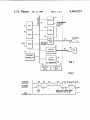
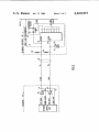
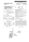
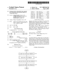
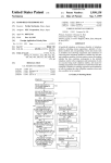
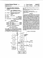
United States Patent [191
[11]
[45]
Eggebrecht et al.
[54] SELF-FACING SERIAL KEYBOARD
Jul. 17, 1984
Dec. ’79.
IBM Personal Computer Reference Manual, Aug. ’81,
pp. D-IO and D-12.
[75] Inventors: Iewis C. Eggebreeht, Rochester,
Minn; Jesus A. Saenz, Coral Springs,
Primary Examiner-Edward J. Wise
Attorney, Agent, or Firm-Sughrue, Mion, Zinn,
Macpeak and Seas
[57]
ABSTRACT
Fla.
International Business Machines
Corporation, Armonk, NY.
[21] Appl. No.: 292,070
[22] Filed:
Aug. 12,1981
A serial keyboard interface (28) connects a self scanning
programmable serialized keyboard (40) to the system
[51]
Int. c1; ............................................ .. oosr 15/02
[52]
u.s.c1. .................................. “ass/zoo; 364/518;
bus (10) of a data processing system. A cable (42) con
taining only a clock wire (52) and a data wire (58) pro
vides the connection. The keyboard transmits a 9-bit
scan out code consisting of a start bit followed by eight
serial data bits. The keyboard clock line (52) is con
nected to the clock or shift terminal of a serial-to-paral
lel shift register encoder (62) for shifting the data bits on
364/900
364/200 MS File, 900 MS File,
364/518; 340/365 R, 365 S
References Cited
[58] Field of Search
[56]
4,460,957
tus”, IBM Technical Disclosure Bulletin, vol. 22, No. 7,
INTERFACE FOR DATA PROCESSING
SYSTEM
[73] Assignee:
Patent Number:
Date of Patent:
data line (58) into the encoder which has eight parallel
U.S. PATENT DOCUMENTS
output data lines (A, B . . . G, H) connected to the
3,501,749
3/1970 Cuccio .............................. .. 364/900
system bus. When the encoder (62) contains a complete
3,980,994
9/1976
scan out frame, the start bit is in the most signi?cant
Ying et a1. . . . . . . . . .
. . . .. 364/200
4,126,898 11/1978 Spangler et a1.
4,386,410
5/1983
364/900
stage (h’) and sets the D-type latch (68) to apply a CPU
interrupt request to the system bus (10). At this time, the
6 output of latch (68) pulls down the data line to
Pandya et al. .................... .. 364/518
FOREIGN PATENT DOCUMENTS
2005448
ground potential, thereby disabling the data line and
preventing further keyboard transmission of data.
When the interrupt request is granted by the CPU, a
4/1979 United Kingdom .
OTHER PUBLICATIONS
M. D. Alger et ai., “Remote Keyboard Interface",
Wireless World, vol. 87, No. 1545, Jun. '81, pp. 77-78.
“An 8048-Based Keyboard/Display Module", Wescon
Conference Record, Sep. 1977, 27/2 pp. 1-4.
clear signal resets latch (68) to remove ground potential
from data line (58) and thereby permit further transmis
sion of data.
14 Claims, 3 Drawing Figures
R. A. DuPont et ai., "Serializer/Deserializer Appara
__
_,
g
. /
2
|
22
'
ill/00s
—
2/
:
m
PROGRAMMABLE
KEYBOARD
RESET
|2\ CPU
l6\
1
1
|
MIA
2o\
1
R05
BM an
|4~
:
2a
\ mu
INT REO '"iié‘é
: 4R
ammo
'
40;
:Tu'ti'nhi?
;
i
s24
I
.
,.______- J
,B\ i
1
DISPLAY
1 32
ADAPTER
I
INTERRUPT
CONTROLLER
;
msx
/26
,
35
|
l
ADAPTER
3°
US. Patent
Jul. 17, 1984
shw 1 of2
5
I;
I
E
5/10
/22
DI/DOs
'
I
l
PROGRAMMABLE
5-2
KEYBOARD
|2\ CPU
‘6
RESET I
|
\
DNA
2o\
|
I
ROS
:
2B\
KYBD
: 42\
RE INEEEE
8m
4,460,957
'|
_~___°_
RAM
:INTERRUPT
‘4w
I
824
I
r--------1
|
4o;
I
'
|a\ I
KEYBOARD
I
so
I 32
DISPLAY
|
ADAPTER
I
\
l
INTERRUPT
W
.
:
CONTROLLER
DISK
ADAPTER
26
I
I
38 3 I
F|G.l
34} I-————|::I [s
DISKETTE
DRIVE
DISKETTE
‘DRWE
H63
KEYBOARD
n n r] n n
CLOCK OUT
D
P
F‘
KEYBOARD
!
'
=
‘
o
1
l
DATA ()UT
,__.| I
I
cPu
INTERRUPT REG‘
53:?‘
LJ
.
I
I I
I
i
'
'
1
o
o
|
'
m
PEEIEIEEEEOE
'
|
o
[_
4,460,957
1
2
More particularly, a three-state system bus 10, includ
ing address, data and control lines, interconnects the
basic components of the computer to provide for the
necessary transfer of address, data and control signals
among these components. The components include, for
SELF-FACING SERIAL KEYBOARD INTERFACE
FOR DATA PROCESSING SYSTEM
TECHNICAL FIELD
This invention relates generally to the ?eld of inter
face circuits for controlling two-way communication
between a keyboard and a data processing system and,
example, the central processing unit (CPU) 12, a dy
namic random access memory (RAM), a multiple chan
nel programmable direct memory access (DMA) con
troller 16, an interrupt controller 18, a read-only storage
more particularly, to a self-pacing interface which per
(ROS) 20, DI/DO’s 22, a display adapter 24, a disk
adapter 26 and a keyboard interface 28.
A cathode ray tube display device 30 may be con
nected by a cable 32 to the display adapter 24. A pair of
mits such communication using only two wires between
the interface and the keyboard.
BACKGROUND OF THE INVENTION
diskette drives 34 and 36 may be connected by a cable
Keyboard entry control circuits or interfaces are
38 to the disk adapter 26. A keyboard 40 is connected by
generally well-known in the prior art; however, they
a cable 42 to the keyboard interface 28.
In this preferred embodiment, the CPU 12 is an Intel
are quite complex and require more than two wires
between the keyboard and the interface, including, in
microprocessor 8088 which is fully disclosed in “The
addition to two wires for carrying clock and data sig
8086 Family User’s Manual, October 1979", published
nals, respectively, status lines for indicating the statuses 20 by
Intel Corporation, Santa Clara, California“. The
of the keyboard and central processing unit, respec
DMA controller is an Intel 8237 high performance
tively. Representative prior art keyboard entry control
programmable DMA controller also fully disclosed in
circuits and interfaces are disclosed in the following
US. Pat. Nos. 3,50l,749; 3,533,078;
4,044,398; 4,126,898 and 4,170,768.
the above Intel Corporation publication. RAM 14 is any
4,038,640;
conventional dynamic memory, such as a T] 4116. Inter
25 rupt controller 18 is an Intel 8259 chip. ROS 20 is also
conventional and may be a Mostek MK 3600, for exam
SUMMARY OF THE INVENTION
ple. DI/DO 22 is a digital input/digital output interface,
The present invention eliminates the need for the
complex keyboard interfaces of the prior art while, at
such as an Intel 8255A general purpose programmable
peripheral interface chip.
the same time, requiring only two wires between the 30 Keyboard interface 28 is the subject of the present
interface and the keyboard. The novel interface of the
invention and is illustrated in detail in FIG. 2.
invention provides the following features:
Keyboard 40 is a programmable self-scanning serial
1. Keyboard data rate and clocking are not tied to any
speci?c clock frequency, and data may be sent at any
rate.
2. The only timing relationships required are set-up
and hold time required with respect to the rising edge of
the keyboard clock; thus, such relationships are easy to
implement in microcode.
3. Capability of supporting two-way communications
between the keyboard and central processing unit
(CPU) of the data processing system.
4. Full handshake and synchronous operation.
5. Relatively few components as compared to prior
ized keyboard which transmits a scan code of 8 series
data bits identi?ed in the various key positions. The
35 scan code also includes a start bit; thus, each serial scan
code is contained in a 9-bit frame headed by the start bit.
Also, in the preferred embodiment keyboard 40 is of the
capacitive matrix type and has 83 key positions. The
keyboard contains its own microprocessor, such as an
40 Intel 8048, and has an OUT CLOCK line, a SENSE
CLOCK line, an OUT DATA line and a SENSE
DATA line. Furthermore, each key is capable of
make/break and typamatic operation. The keyboard
contains self-scanning logic and interface controls
art interfaces.
45 which will support the protocol for keyboard interface
The presence of one or the other of two voltage
28, which protocol is described below.
levels on the two lines connecting the keyboard and
interface functions to control resetting of the keyboard
Keyboard 40, itself, forms no part of the present in
vention and its circuits and construction are found in
and transmission of keyboard data.
copending application Ser. No. 6l,7l9, ?led July 30,
For a better understanding of the present invention, 50 1979 and in the following US. Pat. Nos: 3,786,497;
together with other and further advantages and features
3,92l,l67; and 4,118,611; all of which are incorporated
thereof, reference is made to the following description
herein by reference.
taken in connection with the accompanying drawings,
In general, keyboard interface 28 is self-clocked or
the scope of the invention being pointed out in the ap
self-paced in that it is clocked or paced by the transmis
pended claims.
sion of the keyboard clock and data, completely inde
pendently of any other clock rates in the computer or
BRIEF DESCRIPTION OF THE DRAWINGS
data processing system. When either the system bus is
FIG. 1 is a block diagram of a data processing system
sending a reset command to the keyboard upon power
up or else the interface has not processed a previous
including the novel interface of the invention.
FIG. 2 is a logic block diagram illustrating the details
of the novel interface of the invention.
FIG. 3 is a timing diagram of the operation of the
scan code frame, the keyboard is prevented by its con
trol logic from transmitting data. When a complete scan
code frame has been stored in the interface, a latch is set
to generate an INTERRUPT REQUEST to the CPU
via the interrupt controller. When the INTERRUPT
interface illustrated in FIG. 2.
DESCRIPTION OF THE PREFERRED
EMBODIMENT
FIG. 1 is a block diagram ofa small computer or data
processor, such as a so-called personal computer.
65
REQUEST is granted and the data is transferred to the
CPU, the latch is cleared or reset to signal the keyboard
via its data line that another scan code may be transmit
ted to the interface. Only two lines are required in the
3
4,460,957
cable connecting the interface and the keyboard in
order to perform all of the data, clocking and status
4
sensing functions.
The keyboard tests or senses DATA line 58 via the
SENSE DATA line 57. If the DATA line is DOWN,
then the computer or data processing system has not
More particularly, and as illustrated in FIG. 2, the
SENSE CLOCK line 50 is tied to the keyboard OUT
CLOCK line 52 at junction 54, and an open-collector
processed the previous scan code which had been trans
mitted to the interface 28 (and the Q output of latch 62
is still DOWN or 0). Thus, the keyboard is disabled and
(OC) gate 56 (such as an SN 7407 shown in Texas In
waits for the DATA line 42 to go to l or UP. When, or
struments’ “The TTL Data Book”, second edition,
1976) is connected in the OUT CLOCK line 52 between
if, DATA line 58 is UP, then keyboard 40 transmits via
the keyboard control logic and the junction 54. Further
line 58 a nine-bit frame beginning with a start bit fol
0
lowed by eight series DATA bits representing the scan
code identifying a particular key position of the key
more, the keyboard SENSE DATA line 57 is tied to the
OUT DATA line 58 at the junction 60, and another
open-collector (OC) gate 61 is connected in the DATA
line between junction 60 and the keyboard control
board.
As shown in FIG. 3, the start and eight-data bits are
clocked or shifted into the nine-stage encoder 62 under
the control of the keyboard OUT CLOCK. Note that
the OUT CLOCK is not necessarily periodic, but that
the data bits track the OUT CLOCK; thus, interface 28
is not tied to any specific clock frequency within the
logic. Cable 42, containing ony the CLOCK line 52 and
the DATA line 58, connects keyboard 40 to the novel
keyboard interface 28. Interface 28, itself, requires only
four wires: the keyboard CLOCK and DATA lines, a
system, but rather is paced by the keyboard 40. During
+5 volt (+5 V) and a ground (GND) or zero volt line.
Interface 28 contains a serial-to-parallel shift register 20 the transmission of the scan code frame via DATA line
58, interface 28 is under the control of the keyboard 40,
(74LS299) encoder 62 having a CLOCK terminal 64
and a SERIAL IN terminal 66 for receiving the serial
and latch 68 is in its cleared or reset state with its Q
scan code frame on the DATA line 58 from keyboard
output UP whereby DATA line 58 also UP.
40. Encoder 62 has nine stages and eight corresponding
However, when all nine bits of the scan code frame
parallel DATA output lines, labeled A, B . . . E, H and 25 have been shifted or clocked into the encoder 62, the
start bit in the most signi?cant stage is clocked by the
a start line, labeled h’. Stage A is the lowest ordered or
OUT CLOCK to the D input of latch 48, thereby set
least significant stage, and stage h’ is the highest ordered
or most signi?cant stage. The most signi?cant stage
ting the latch, raising the Q output to send the INTER
output line h’ is connected to the D input terminal of a
RUPT REQUEST to the system bus, and lowering the
D-type edge-triggered latch 68. CLOCK line 52 is con 30 Q output, thus applying ground potential to DATA line
nected to the CLK terminal of latch 68. The Q or set
58 and causing the DATA line to go DOWN; since the
keyboard will sense by its SENSE DATA line 57 the
output terminal of latch 68 is connected to the system
DOWN condition of DATA line 58, the keyboard is
bus 10 and transmits an INTERRUPT REQUEST
prevented from transmitting any additional data. How
ggnal to the CPU 12 via the interrupt controller 18. The
Q or reset output line of latch 68 is connected through 35 ever, after the INTERRUPT REQUEST has been
granted and the eight data bits transmitted in parallel
another open-collector (OC) gate 70 to the keyboard
from the encoder via DI/DO 22 to the system bus 10, a
DATA line 58. The CLR or reset terminal of latch 68 is
also connected to the system bus 10 and receives a
CLEAR or reset signal from the CPU when an IN
TERRUPT REQUEST has been granted and the eight
CLEAR signal from the CPU is applied to the CLR
terminal of latch 68, thereby clearing or resetting the
40
latch to cause the Q output to go UP and permitting
DATA line 58 to return to the UP state which is sensed
parallel data bits have been transmitted from encoder 62
via DI/DO 22 to a register in the CPU.
The OC gates 56, 61 and 70 are functionally switches
which, when closed, place ground or a zero (0) voltage
by the keyboard SENSE DATA line 56 to permit the
next scan code frame to be transmitted to the interface
28.
While there has been described what is at present
on the line to which their outputs are connected. In 45
considered to be the preferred embodiment of this in
other words, ifa l or UP level appears on a gate input,
vention, it will be obvious to those skilled in the art that
then the gate output is a l (+5 V) or UP.
various changes and modifications may be made therein
without departing from the invention, and it is, there
Now, the operation and protocol of keyboard inter
face 28 will be described with reference to FIG. 2 and
the timing diagram of FIG. 3.
50 fore, intended to cover all such changes and modifica
tions as fall within the true spirit and scope ofthe inven
tion.
We claim:
1. In a data processing system including a system bus
First, both the CLOCK line 52 and the DATA line 58
are tied to + 5 volts. The existence ofa +5 volts poten
tial on the line will be referred to as the UP state of the
line, whereas the existence of O or ground potential on
a line will be referred to as the DOWN state.
55
When a key is depressed on keyboard 40, both the
OUT CLOCK and DATA are generated. Initially the
keyboard sets its OUT CLOCK to a l. The keyboard
then tests or senses the CLOCK line 52 via the SENSE
for transferring address, data and control signals among
a central processing unit, a memory and a self-scanning
serial keyboard, all connected to the bus, said keyboard
having a clock line for transmitting a keyboard out
clock signal and a data line for transmitting a serial scan
CLOCK line 50 to determine whether the CLOCK line 60 out code in a frame headed by a start bit followed by a
predetermined number of serial data bits identifying a
is UP or DOWN. If the CLOCK line 52 is DOWN, the
key position, an improved interface for providing two
system is requesting keyboard 40 to execute a reset by
way communication between the bus and the keyboard,
virtue of a ground signal (RESET) from DI/DO 22 on
the reset line 72. This condition can occur upon power
up, and causes the keyboard to reset all of its circuits. 65
However, if the keyboard senses an UP state on
CLOCK line 52, then keyboard 40 is enabled and tries
to raise the DATA line 58.
and comprising:
serial-to-parallel shift register encoder means for stor
ing in parallel the frame of serial bits under the
control of the clock signal and having (1) a clock
terminal connected to said keyboard clock line, (2)
5
4,460,957
6
8. An improved interface as de?ned in claim 7 further
comprising means, coupled to the bus, for applying to
said clock line a disabling signal to disable the out clock
a serial data input terminal connected to said key
board data line, (3) said predetermined number of
parallel output data lines connected to the bus, and
(4) a control line coupled to the most signi?cant
stage of said encoder, said encoder having the same
signal.
number of stages as the number of bits in a frame,
whereby, when said encoder contains said start bit
comprising gate means, coupled between said data line
and said Q reset output terminal, responsive to said
signal and said predetermined number of data bits,
disabling signal for applying ground potential to said
a control signal is produced on said control line;
data line.
10. In a data processing system including a system bus
9. An improved interface as de?ned in claim 7 further
and
control means, responsive to said control signal and
to said keyboard out clock signal, for applying a
central processing unit interrupt signal to the bus
and for applying to said data line a disabling signal
which prevents further transmission of data bits by 5
the keyboard,
for transferring address, data and control signals among
an interruptable central processing unit, a memory and
a self-scanning serial keyboard, all connected to the bus,
said keyboard having a clock line for transmitting a
keyboard out clock signal and a data line for transmit
ting a serial scan out code in a frame headed by a start
bit followed by a predetermined number of serial data
bits identifying a key position, an improved interface for
providing two-way communication between the bus
said control means also being responsive to a clear
signal from the central processing unit to remove
the disabling signal from the data line when said
data bits have been transferred from said encoder 20 and the keyboard, and comprising:
serial-to-parallel shift register encoder means for stor
means to said bus, thereby permitting transmission
ing in parallel the frame of serial bits under the
of another scan code frame from the keyboard to
control of the clock signal and having (I) a clock
said encoder means.
terminal coupled to said keyboard clock line, (2) a
2. An improved interface as de?ned in claim 1
serial data input terminal connected to said key
wherein said control means comprises a D-type edge 25
board data line, (3) said predetermined number of
triggered latch having its D input tenninal connected to
parallel output data lines connected to the bus, and
said control line, its clock terminal connected to said
(4) a control line coupled to the most signi?cant
clock line, its Q set output terminal connected to the
stage of said encoder, said encoder having at least
bus, its Q reset output terminal connected to the data
the same number of stages as the number of bits in
line, and its clear terminal connected to the bus,
a frame, whereby, when said encoder contains said
whereby said control signal sets said latch to generate
start bit signal and said predetermined number of
said interrupt signal on _s_aid Q output terminal and said
data hits, a control signal is produced on said con~
disabling signal on said Q reset output terminal when an
trol line; and
entire scan code frame is stored in said encoder, said
control means, responsive to said control signal and
clear signal being applied to said clear terminal to reset 35
to said keyboard out clock signal, for providing an
said latch and cause said Q reset output terminal to
interrupt signal to said central processing unit and
remove said disabling signal from said data line.
for applying to said data line a disabling signal
3. An improved interface as de?ned in claim 2 further
which prevents further transmission of data bits by
comprising means, connected to the bus; for applying to
said keyboard,
said clock line a disabling signal to disable the out clock 40
said control means also being responsive to a clear
signal and to reset the keyboard.
signal from the central processing unit to remove
4. An improved interface as de?ned in claim 2 further
the disabling signal from the data line when said
comprising gate means, coupled between said data line
data bits have been transferred from said encoder
and said Q reset output terminal, responsive to said
disabling signal for applying ground potential to said
45
data line.
5. An improved interface as de?ned in claim 1 further
comprising means, connected to the bus, for applying to
said clock line a disabling signal to disable the out clock
\ means to said bus, thereby permitting transmission
of another scan code frame from the keyboard to
said encoder means.
11. An improved interface as de?ned in claim 10
further comprising means, coupled to the bus, for apply
ing to said clock line a disabling signal to disable the out
clock signal.
6. An improved interface as de?ned in claim 1 further
12. In a data processing system including a system bus
comprising means, connected to the bus, for applying to
for transferring address, data and control signals among
said clock line a disabling signal to disable the out clock
an interruptable central processing unit, a memory and
signal and to reset the keyboard.
7. An improved interface as de?ned in claim 1 55 a self-scanning serial keyboard, all connected to the bus,
said keyboard having a clock line for transmitting a
wherein said control means comprises a D-type edge
keyboard out clock signal and a data line for transmit
triggered latch having its D input terminal coupled to
signal.
said control line, its clock terminal coupled to said clock
ting a serial scan out code in a frame headed by a start
line, its Q set output terminal providing said interrupt
signal, its Q reset output terminal coupled to disable the
bit followed by a predetermined number of serial data
bits identifying a key position, an improved method for
providing two-way communication between the bus
data line, and its clear terminal coupled to the bus,
whereby said control signal sets said latch to generate
said interrupt signal on said Q output terminal and said
disabling signal on said Q reset output terminal when an
entire scan code frame is stored in said encoder, said 65
and the keyboard, comprising the steps of:
serially shifting into a serial-to-parallel shift register
encoder a frame of serial bits, received on said data
line under the control of the keyboard clock signal;
clear signal being applied to said clear terminal to reset
when a start bit having a predetermined ?xed state is
said latch and cause said Q reset output terminal to
remove said disabling signal from said data line.
shift register encoder, providing an interrupt signal
received in a most-signi?cant bit position of said
7
4,460,957
8
mission of another scan code frame from said key
board to said shift register encoder.
13. An improved communication method as claimed
to said central processing unit and simultaneously
applying to said data line a disabling signal for
preventing further transmission of data bits by said
in claim 12 further comprising the step of disabling said
5 clock signal in response to a reset signal from said cen
keyboard; and
tral processing means.
removing said interrupt signal in response to a clear
14. An improved communication method as claimed
in claim 12 wherein said step of applying said disabling
signal to said data line comprises applying a ground
potential to said data line.
signal from said central processing means when
said data bits have been transferred from said en
coder means to said bus, thereby permitting trans
i
20
25
30
35
45
55
i
‘I
*
$