1
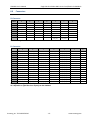
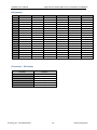
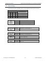
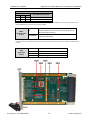
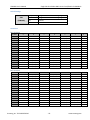
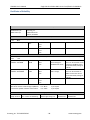
VPX4812 Single-Slot 3U VPX Bus XMC Carrier Card with P16 Support VPX Switch Card USER’S MANUAL ACROMAG INCORPORATED 30765 South Wixom Road Wixom, MI 48393-7037 U.S.A. Tel: (248) 295-0310 Fax: (248) 624-9234 Copyright 2014, Acromag, Inc., Printed in the USA. Data and specifications are subject to change without notice. 8501-022A VPX4812 User’s Manual Single-Slot 3U VPX Bus XMC Carrier Card/Switch Card Module The information contained in this manual is subject to change without notice. Acromag, Inc. makes no warranty of any kind with regard to this material, including, but not limited to, the implied warranties of merchantability and fitness for a particular purpose. Further, Acromag, Inc. assumes no responsibility for any errors that may appear in this manual and makes no commitment to update, or keep current, the information contained in this manual. No part of this manual may be copied or reproduced in any form, without the prior written consent of Acromag, Inc. IMPORTANT SAFETY CONSIDERATIONS It is very important for the user to consider the possible adverse effects of power, wiring, component, sensor, or software failures in designing any type of control or monitoring system. This is especially important where economic property loss or human life is involved. It is important that the user employ satisfactory overall system design. It is agreed between the Buyer and Acromag, that this is the Buyer's responsibility. Acromag, Inc. Tel: 248-295-0310 -2- www.acromag.com VPX4812 User’s Manual 1.0 Single-Slot 3U VPX Bus XMC Carrier Card/Switch Card Module General Information ..................................................................................................................... 5 Key Features ................................................................................................................................. 5 Introduction .................................................................................................................................. 6 Module and Backplane Profiles ..................................................................................................... 6 Build Levels ................................................................................................................................... 7 2.0 Ordering Information .................................................................................................................... 8 3.0 Preparation For Use ...................................................................................................................... 9 Unpacking and Inspection ............................................................................................................. 9 4.0 Operational Block Diagram ......................................................................................................... 10 5.0 Board Layout............................................................................................................................... 11 6.0 Connectors ................................................................................................................................. 12 P0 Connector .............................................................................................................................. 12 P1 Connector .............................................................................................................................. 12 P2 Connector .............................................................................................................................. 13 J15 Connector ............................................................................................................................. 13 J16 Connector ............................................................................................................................. 14 J5 Connector – JTAG Header ....................................................................................................... 14 7.0 Switch Settings............................................................................................................................ 15 Front Panel Layout ...................................................................................................................... 17 8.0 Handling ..................................................................................................................................... 18 ESD Safe Work Area Guidelines................................................................................................... 18 9.0 Installation .................................................................................................................................. 19 Board Keying ............................................................................................................................... 19 Installation Notes ........................................................................................................................ 19 10.0 Specifications .............................................................................................................................. 20 Physical ....................................................................................................................................... 20 Power Requirements .................................................................................................................. 20 Power Consumption ................................................................................................................... 20 Auxiliary Supply .......................................................................................................................... 21 Power-Up/Reset Sequence ......................................................................................................... 21 Bus Compliance .......................................................................................................................... 21 Form Factor ................................................................................................................................ 21 Flammability ............................................................................................................................... 21 Environmental ............................................................................................................................ 22 EMI/EMC Regulatory Compliance ............................................................................................... 22 Acromag, Inc. Tel: 248-295-0310 -3- www.acromag.com VPX4812 User’s Manual 11.0 Single-Slot 3U VPX Bus XMC Carrier Card/Switch Card Module Service and Repair ...................................................................................................................... 23 Service and Repair Assistance ..................................................................................................... 23 Preliminary Service Procedure .................................................................................................... 23 Where to Get Help ...................................................................................................................... 23 Appendix A – Accessory Modules ............................................................................................................ 24 TRANS-V112................................................................................................................................ 24 Certificate of Volatility ............................................................................................................................. 28 Revision History ....................................................................................................................................... 29 Acromag, Inc. Tel: 248-295-0310 -4- www.acromag.com VPX4812 User’s Manual 1.0 Single-Slot 3U VPX Bus XMC Carrier Card/Switch Card Module General Information The VPX4812 is an XMC Carrier Card Module in the 3U VPX form factor, targeted for processing, communications, and display applications in the commercial, military, and aerospace markets. The VPX4812 provides support for Rear I/O connections from the XMC P16 connector. The TRANS-V112 is the Rear Transition Module for the VPX4812 used to bring out Rear I/O connections through the backplane. The VPX4812 supports up to four VPX Fat Pipe (x4) connections to other cards in the system at Gen 2.0 speeds. The VPX4812 can be used as a switch card allowing an upstream Fat Pipe or Double Fan Pipe connection – typically to a CPU – to communicate with up to three downstream Fat Pipe connections or a single Double Fat Pipe connection. The VPX4812 also provides support for a VPX Double Fat Pipe (x8) connection to an XMC card at Gen 2.0 speeds. Key Features Acromag, Inc. Tel: 248-295-0310 24-Channel 5-Port PCI Express Gen. 2.0 Switch The XMC site is PCIe 8-Lanes Gen. 2.0 Module conforms to VPX Spec. VITA 46.0, 46.4, and 46.9 The XMC site supports X24s+X8d+X12d I/O mapping (VITA 46.9) 16 Lanes PCI Express to backplane (VITA 46.0 and 46.4) Supports Non-Transparent Bridging Applications 3U VPX form factor supporting OpenVPX/VITA 65 Air and conduction cooled variants available REDI covers supporting VITA 48 available -5- www.acromag.com VPX4812 User’s Manual Single-Slot 3U VPX Bus XMC Carrier Card/Switch Card Module Introduction The VPX4812 has two primary functions that can be utilized in a VPX system simultaneously. 1. XMC Carrier Card – The VPX4812 supports a Double Fat Pipe (x8) connection from an XMC module to the on-board PCIe switch. The voltage used to power the XMC module can be toggled between 5V or 12V using a DIP switch located on the VPX4812. 2. VPX Switch Card – The VPX4812 contains a 24-lane 5-port PCIe switch capable of Gen 2.0 speeds. When utilizing the VPX4812 as a switch card, a CPU module configured to be an upstream port can communicate with up to three downstream VPX cards in the system as well as an XMC module on the 4812. The VPX4812 supports the use of non-transparent bridging using the on-board PCIe switch. By utilizing non-transparent bridging (NTB), the VPX4812 can be used to implement multi-hosted topologies including intelligent adapter cards, dual-host systems with redundancy, and even blade server systems. Module and Backplane Profiles The VPX4812 conforms to module profile MOD3-SWH-4F-16.4.5-2 of the VITA 65 specification. The VPX4812 conforms to switch slot profile SLT3-SWH-4F-14.4.4 of the VITA 65 specification. The VPX 4812 is intended for use in backplane profiles BKP3-CEN06-15.2.12-n of the VITA 65 specification. Use of this module in an incompatible backplane profile could result in damage to this module or others in the chassis. VPX4812 Suggested Backplane Topology Acromag, Inc. Tel: 248-295-0310 -6- www.acromag.com VPX4812 User’s Manual Single-Slot 3U VPX Bus XMC Carrier Card/Switch Card Module Build Levels The VPX4812 is available in three electrically compatible build levels, each of which is carefully tailored to a particular set of requirements and environments. All three levels fully support the power and versatility of VPX, so no matter how large or diversified your project, absolute compatibility is assured at all stages of development. The three build levels have three basic mechanical configurations, both in accordance with the VITA 46.0 VPX standard and the VITA 48 REDI standard: 1. Air (convection) cooled modules are intended for use in standard industrial chassis. 2. Conduction-cooled modules are intended for use in sealed Air Transportable Racking (ATR) and other conduction-cooled environments. 3. REDI cover, Conduction-cooled modules are intended for use in sealed Air Transportable Racking (ATR) and other conduction-cooled environments. Acromag, Inc. Tel: 248-295-0310 -7- www.acromag.com VPX4812 User’s Manual 2.0 Single-Slot 3U VPX Bus XMC Carrier Card/Switch Card Module Ordering Information VPX4812 Available Models VPX4812-XX VPX4812-CC-XX VPX4812-REDI-XX Air-cooled Model Conduction-cooled Model REDI XX = Solder L = Lead solder LF = Lead-free solder Acromag, Inc. Tel: 248-295-0310 -8- www.acromag.com VPX4812 User’s Manual 3.0 Single-Slot 3U VPX Bus XMC Carrier Card/Switch Card Module Preparation For Use Unpacking and Inspection Upon receipt of this product, inspect the shipping carton for evidence of mishandling during transit. If the shipping carton is badly damaged or water stained, request that the carrier's agent be present when the carton is opened. If the carrier's agent is absent when the carton is opened and the contents of the carton are damaged, keep the carton and packing material for the agent's inspection. For repairs to a product damaged in shipment, refer to the Acromag Service Policy to obtain return instructions. It is suggested that salvageable shipping cartons and packing material be saved for future use in the event the product must be shipped. This board is physically protected with packing material and electrically protected with an anti-static bag during shipment. It is recommended that the board be visually inspected for evidence of mishandling prior to applying power. The board utilizes static sensitive components and should only be handled at a static-safe workstation. IMPORTANT: Adequate air circulation must be provided to prevent a temperature rise above the maximum operating temperature. Adequate air circulation must be provided to prevent a temperature rise above the maximum operating temperature and to prolong the life of the electronics. If the installation is in an industrial environment and the board is exposed to environmental air, careful consideration should be given to air-filtering. Acromag, Inc. Tel: 248-295-0310 -9- www.acromag.com VPX4812 User’s Manual 4.0 Single-Slot 3U VPX Bus XMC Carrier Card/Switch Card Module Operational Block Diagram Acromag, Inc. Tel: 248-295-0310 - 10 - www.acromag.com VPX4812 User’s Manual 5.0 Single-Slot 3U VPX Bus XMC Carrier Card/Switch Card Module Board Layout Acromag, Inc. Tel: 248-295-0310 - 11 - www.acromag.com VPX4812 User’s Manual 6.0 Single-Slot 3U VPX Bus XMC Carrier Card/Switch Card Module Connectors P0 Connector P0 Wafer 1 A B C D E F G +3.3 V +3.3 V +3.3 V Unused +12 V +12 V +12 V 2 +3.3 V +3.3 V +3.3 V Unused +12 V +12 V +12 V 3 +5 V +5 V +5 V Unused +5 V +5 V +5 V 4 NVRAM_LOCK PLT_RST# GND -12V_AUX GND Unused Unused 5 SMB_DATA SMB_CLK GND +3.3V AUX GND Unused Unused 6 GA0# GA1# GND +12V_AUX GND GA2# GA3# 7 Unused Unused GND Unused Unused GND Unused 8 GND Unused Unused GND PCIe VPX REF_CLK P PCIe VPX REF_CLK N GND # = Low true signal P1 Connector P1 Wafer A B C D E F G 1 PCIE_VPX_P0_RXP PCIE_VPX_P0_RXN GND PCIE_VPX_P0_TXP PCIE_VPX_P0_TXN GND Unused 2 GND PCIE_VPX_P1_RXP PCIE_VPX_P1_RXN GND PCIE_VPX_P1_TXP PCIE_VPX_P1_TXN GND 3 PCIE_VPX_P2_RXP PCIE_VPX_P2_RXN GND PCIE_VPX_P2_TXP PCIE_VPX_P2_TXN GND Unused 4 GND PCIE_VPX_P3_RXP PCIE_VPX_P3_RXN GND PCIE_VPX_P3_TXP PCIE_VPX_P3_TXN GND 5 PCIE_VPX_P4_RXP PCIE_VPX_P4_RXN GND PCIE_VPX_P4_TXP PCIE_VPX_P4_TXN GND Unused 6 GND PCIE_VPX_P5_RXP PCIE_VPX_P5_RXN GND PCIE_VPX_P5_TXP PCIE_VPX_P5_TXN GND 7 PCIE_VPX_P6_RXP PCIE_VPX_P6_RXN GND PCIE_VPX_P6_TXP PCIE_VPX_P6_TXN GND Unused 8 GND PCIE_VPX_P7_RXP PCIE_VPX_P7_RXN GND PCIE_VPX_P7_TXP PCIE_VPX_P7_TXN GND 9 PCIE_VPX_P8_RXP PCIE_VPX_P8_RXN GND PCIE_VPX_P8_TXP PCIE_VPX_P8_TXN GND Unused 10 GND PCIE_VPX_P9_RXP PCIE_VPX_P9_RXN GND PCIE_VPX_P9_TXP PCIE_VPX_P9_TXN GND 11 PCIE_VPX_P10_RXP PCIE_VPX_P10_RXN GND PCIE_VPX_P10_TXP PCIE_VPX_P10_TXN GND Unused 12 GND PCIE_VPX_P11_RXP PCIE_VPX_P11_RXN GND PCIE_VPX_P11_TXP PCIE_VPX_P11_TXN GND 13 PCIE_VPX_P12_RXP PCIE_VPX_P12_RXN GND PCIE_VPX_P12_TXP PCIE_VPX_P12_TXN GND Unused 14 GND PCIE_VPX_P13_RXP PCIE_VPX_P13_RXN GND PCIE_VPX_P13_TXP PCIE_VPX_P13_TXN GND 15 PCIE_VPX_P14_RXP PCIE_VPX_P14_RXN GND PCIE_VPX_P14_TXP PCIE_VPX_P14_TXN GND Unused 16 GND PCIE_VPX_P15_RXP PCIE_VPX_P15_RXN GND PCIE_VPX_P15_TXP PCIE_VPX_P15_TXN GND RX is defined as a signal that is an input to the VPX4812. TX is defined as a signal that is an output from the VPX4812. Acromag, Inc. Tel: 248-295-0310 - 12 - www.acromag.com VPX4812 User’s Manual Single-Slot 3U VPX Bus XMC Carrier Card/Switch Card Module P2 Connector P2 Wafer A B C D E F G 1 J16_SIO11_P J16_SIO11_N GND J16_SIO10_P J16_SIO10_N GND Unused 2 GND J16_SIO9_P J16_SIO9_N GND J16_SIO8_P J16_SIO8_N GND 3 J16_SIO7_P J16_SIO7_N GND J16_SIO6_P J16_SIO6_N GND Unused 4 GND J16_SIO5_P J16_SIO5_N GND J16_SIO4_P J16_SIO4_N GND 5 J16_SIO3_P J16_SIO3_N GND J16_SIO2_P J16_SIO2_N GND Unused 6 GND J16_SIO1_P J16_SIO1_N GND J16_SIO0_P J16_SIO0_N GND 7 J16_DP01_N J16_DP01_P GND J16_DP00_N J16_DP00_P GND Unused 8 GND J16_DP03_N J16_DP03_P GND J16_DP02_N J16_DP02_P GND Unused 9 J16_DP11_N J16_DP11_P GND J16_DP10_N J16_DP10_P GND 10 GND J16_DP13_N J16_DP13_P GND J16_DP12_N J16_DP12_P GND 11 J16_DP05_N J16_DP05_P GND J16_DP04_N J16_DP04_P GND Unused 12 GND J16_DP07_N J16_DP07_P GND J16_DP06_N J16_DP06_P GND 13 J16_DP09_N J16_DP09_P GND J16_DP08_N J16_DP08_P GND Unused 14 GND J16_DP15_N J16_DP15_P GND J16_DP14_N J16_DP14_P GND 15 J16_DP17_N J16_DP17_P GND J16_DP16_N J16_DP16_P GND Unused 16 GND J16_DP19_N J16_DP19_P GND J16_DP18_N J16_DP18_P GND J15 Connector 1 A B C D E F PCIE_XMC_P0_RXP PCIE_XMC_P0_RXN +3.3V PCIE_XMC_P1_RXP PCIE_XMC_P1_RXN VPWR 2 GND GND NC GND GND XMC_RSTI# 3 PCIE_XMC_P2_RXP PCIE_XMC_P2_RXN +3.3V PCIE_XMC_P3_RXP PCIE_XMC_P3_RXN VPWR 4 GND GND JTAG_TCK GND GND XMC_RSTO# 5 PCIE_XMC_P4_RXP PCIE_XMC_P4_RXN +3.3V PCIE_XMC_P5_RXP PCIE_XMC_P5_RXN VPWR 6 GND GND JTAG_TMS GND GND +12V 7 PCIE_XMC_P6_RXP PCIE_XMC_P6_RXN +3.3V PCIE_XMC_P7_RXP PCIE_XMC_P7_RXN VPWR 8 GND GND JTAG_TDI GND GND -12V_AUX 9 NC NC NC NC NC VPWR 10 GND GND JTAG_TDO GND GND GA0# 11 PCIE_XMC_P0_TXP PCIE_XMC_P0_TXN NC PCIE_XMC_P1_TXP PCIE_XMC_P1_TXN VPWR 12 GND GND GA1# GND GND NC 13 PCIE_XMC_P2_TXP PCIE_XMC_P2_TXN +3.3V_AUX PCIE_XMC_P3_TXP PCIE_XMC_P3_TXN VPWR SMB_DATA 14 GND GND GA2# GND GND 15 PCIE_XMC_P4_TXP PCIE_XMC_P4_TXN NC PCIE_XMC_P5_TXP PCIE_XMC_P5_TXN VPWR 16 GND GND NVRAM_LOCK GND GND SMB_CLK 17 PCIE_XMC_P6_TXP PCIE_XMC_P6_TXN NC PCIE_XMC_P7_TXP PCIE_XMC_P7_TXN NC 18 GND GND NC GND GND NC 19 PCIE_VPX REF_CLK P PCIE_VPX REF_CLK N NC NC ROOT0# NC # = Low true signal Acromag, Inc. Tel: 248-295-0310 - 13 - www.acromag.com VPX4812 User’s Manual Single-Slot 3U VPX Bus XMC Carrier Card/Switch Card Module J16 Connector 1 A B C D E F J16_DP00_P J16_DP00_N NC J16_DP01_P J16_DP01_N NC 2 GND GND NC GND GND NC 3 J16_DP02_P J16_DP02_N NC J16_DP03_P J16_DP03_N NC 4 GND GND NC GND GND NC 5 J16_DP04_P J16_DP04_N NC J16_DP05_P J16_DP05_N NC 6 GND GND NC GND GND NC 7 J16_DP06_P J16_DP06_N NC J16_DP07_P J16_DP07_N NC 8 GND GND J16_SIO10_N GND GND J16_SIO11_N 9 J16_DP08_P J16_DP08_N J16_SIO10_P J16_DP09_P J16_DP09_N J16_SIO11_P 10 GND GND J16_SIO8_N GND GND J16_SIO9_N 11 J16_DP10_P J16_DP10_N J16_SIO8_P J16_DP11_P J16_DP11_N J16_SIO9_P J16_SIO7_N 12 GND GND J16_SIO6_N GND GND 13 J16_DP12_P J16_DP12_N J16_SIO6_P J16_DP13_P J16_DP13_N J16_SIO7_P 14 GND GND J16_SIO4_N GND GND J16_SIO5_N 15 J16_DP14_P J16_DP14_N J16_SIO4_P J16_DP15_P J16_DP15_N J16_SIO5_P 16 GND GND J16_SIO2_N GND GND J16_SIO3_N 17 J16_DP16_P J16_DP16_N J16_SIO2_P J16_DP17_P J16_DP17_N J16_SIO3_P 18 GND GND J16_SIO0_N GND GND J16_SIO1_N 19 J16_DP18_P J16_DP18_N J16_SIO0_P J16_DP19_P J16_DP19_N J16_SIO1_P J5 Connector – JTAG Header Pin Number 1 Description 2 JTAG_TDO JTAG_TDI 3 GND 4 JTAG_TCK 5 JTAG_TMS 6 JTAG_VREF Acromag, Inc. Tel: 248-295-0310 - 14 - www.acromag.com VPX4812 User’s Manual 7.0 Single-Slot 3U VPX Bus XMC Carrier Card/Switch Card Module Switch Settings The following describes the VPX4812 switches with their default positions and their functions. SW1 – Upstream Port Selection Switch Position Selected Upstream Port 1 2 3 4 ON ON ON ON VPX Fat Pipe A (default) OFF ON ON ON VPX Fat Pipe B OFF ON OFF ON VPX Fat Pipe C ON OFF OFF ON VPX Fat Pipe D ON ON ON OFF XMC 1-2 (default) FRU uses 3.3V 2-3 FRU uses 3.3V_AUX 4-5 (default) Orb ground is connected to digital ground. 5-6 Orb ground is isolated from digital ground. Orb ground is the front panel and the VPX key-guides. SW2 (FRUSEL & ORBGND) SW3-1 (STATION 0 PORT CONFIG) ON (default) VPX Fat Pipe A = x4, VPX Fat Pipe B = x4 OFF VPX Fat Pipe A = x8, VPX Fat Pipe B = Disabled SW3-2 (STATION 1 PORT CONFIG) ON VPX Fat Pipe C = x8, VPX Fat Pipe D = Disabled OFF (default) VPX Fat Pipe C = x4, VPX Fat Pipe D = x4 SW3-3 (PCIE LINK SPEED) ON Force Gen 1.0 Speed Only OFF (default) Allow Gen 1.0 & Gen 2.0 Speeds SW3-4 (XMC VPWR VOLT SELECT) ON VPWR = +12V OFF (default) VPWR = +5V Acromag, Inc. Tel: 248-295-0310 - 15 - www.acromag.com VPX4812 User’s Manual Single-Slot 3U VPX Bus XMC Carrier Card/Switch Card Module SW4-1:3 – Upstream NT Port Selection Switch Position Selected NT Upstream Port 1 2 3 ON ON ON VPX Fat Pipe A ON OFF ON VPX Fat Pipe B OFF OFF OFF NT Mode Disabled (default) Note: In addition to the switch configuration, there are settings for the PEX8624 that must be programmed to the onboard EEPROM device to enable Non-Transparent Mode. SW4-4 (SYSTEM CLOCK SELECT) ON (Common) Uses the 100MHz reference clock pins on the VPX bus generated by the CPU board for PCIe timing. (Pins E8 & F8 on the VPX P0 connector) OFF (default) (Non-Common) Uses the 100MHz reference clock generated on board for PCIe timing. Note: Best system stability may be achieved with the use of a 100MHz common clock connection from the SBC, especially at Gen 2.0 link speeds. If the system does not provide a common clock then non-common clock mode must be used. SW5 (JTAG VREF SELECT) 1-2 (default) 2-3 JTAG_VREF = +3.3V JTAG_VREF = +2.5V 4-5 5-6 Unused Unused Acromag, Inc. Tel: 248-295-0310 - 16 - www.acromag.com VPX4812 User’s Manual Single-Slot 3U VPX Bus XMC Carrier Card/Switch Card Module Front Panel Layout VPX4812 Front Panel On the front panel of air-cooled VPX4812 assemblies, there are 5 port status LED’s. The first four LED’s indicate the PCIe link status for each of the four Fat Pipe connections to other slots on the VPX backplane. The fifth LED on the front panel indicates the PCIe link status of an XMC module connected to the VPX4812. The table below describes what the LED On/Off patterns indicate about the corresponding port states. Port Status LED On/Off Patterns, by State State Link is down Link is up, Gen 2.0 speed, all Lanes are up Link is up, Gen 2.0 speed, reduced Lanes are up Link is up, Gen 1.0 speed, all Lanes are up Link is up, Gen 1.0 speed, reduced Lanes are up Acromag, Inc. Tel: 248-295-0310 LED Pattern Off On Blinking, 0.5 seconds On, 0.5 seconds Off Blinking, 1.5 seconds On, 0.5 seconds Off Blinking, 0.5 seconds On, 1.5 seconds Off - 17 - www.acromag.com VPX4812 User’s Manual 8.0 Single-Slot 3U VPX Bus XMC Carrier Card/Switch Card Module Handling Modules should be handled in ESD-safe work areas in order to prevent damage to sensitive components from electrostatic discharges. These areas must be designed and maintained to prevent ESD damage. ESD Safe Work Area Guidelines 1. Module should be handled at properly designated work areas only. 2. Designated ESD safe work areas must be checked periodically to ensure their continued safety from ESD. The areas should be monitored for the following: a. Proper grounding methods. b. Static dissipation of work surfaces. c. Static dissipation of floor surfaces. d. Operation of ion blowers and ion air guns. 3. Designated work areas must be kept free of static generating materials such as Styrofoam, vinyl, plastic, fabrics, or any other static generating materials. 4. Work areas must be kept clean and neat in order to prevent contamination of the work area. 5. Modules should be handled by the edges. Avoid touching component leads. NOTE: When not installed in a system, modules must be enclosed in shielded bags or boxes. There are three types of ESD protective enclosure materials this module was shipped in an approved ESD bag. 6. Whenever handling the module the operator must be properly grounded by one of the following: a. Wearing a wrist strap connected to earth ground. b. Wearing heel grounders and have both feet on a static dissipative floor surface. 7. Stacking of modules should be avoided to prevent physical damage. Acromag, Inc. Tel: 248-295-0310 - 18 - www.acromag.com VPX4812 User’s Manual 9.0 Single-Slot 3U VPX Bus XMC Carrier Card/Switch Card Module Installation IMPORTANT: The VPX4812 has been specifically design for use with 3U VPX backplanes and my not be compatible with some 6U backplanes. Plugging the board into an unsupported 6U VPX backplane may cause permanent damage. Consult the enclosure documentation to ensure that the VPX4812’s power requirements are compatible with those supplied by the backplane. Board Keying The 3U VPX backplane specification requires all backplane slots to have two guide pins: one above the J0 connector and one below the J2 connector. As well as providing correct alignment, these pins are keyed to prevent cards from being inserted into incorrect backplane slot(s) to avoid electrical incompatibility. The VPX4812 has receptacles for these guide pins (see the Connectors section). By default, these are not keyed. Please contact the factory to discuss keying requirements. Installation Notes 1. Keying may dictate the backplane slot(s) into which the VPX4812 can be inserted. 2. Air-cooled versions have an ejector handle to ensure that the backplane connectors mate properly with the backplane. The captive screws at the top and bottom of the front panel allow the VPX4812 to be tightly secured in position, which provides continuity with system chassis ground. 3. Conduction-cooled and REDI versions have screw driven wedge locks at the top and bottom of the board to provide the necessary mechanical/thermal interface. Correct adjustment requires a calibrated torque wrench set to between 0.6 and 0.8 Nm. Acromag, Inc. Tel: 248-295-0310 - 19 - www.acromag.com VPX4812 User’s Manual Single-Slot 3U VPX Bus XMC Carrier Card/Switch Card Module 10.0 Specifications Physical Height: Width: Board Thickness: 100.00 mm (3.937 in.) 160.00 mm (6.299 in.) 1.575 mm (0.062 in.) Unit Weight (air-cooled): Unit Weight (conduction-cooled): Unit Weight (REDI): 5.10 Oz (0.14 Kg) 8.34 Oz (0.24 Kg) 12.37 Oz (0.35 Kg) Power Requirements The VPX4812 requires +3.3V and +5V from the VPX backplane. The +/-12V supplies are used only if required by the XMC module. Power Consumption No XMC Card Installed: +3.3V: <1W +5V: 2.62W typ. 5.43W max +12V: 0W XMC Card Installed: +3.3V: <1W +5V: 80.43W max 5.43W max +12V: 0W max 60W max (VPWR = 5V) (VPWR = 12V) (VPWR = 5V) (VPWR = 12V) Note: The power supplied to the XMC card can be toggled between 5V or 12V depending on the card’s requirements and/or the power supply’s available capacities. Caution If VPWR is set to 12V, you must ensure that the XMC card is capable of handling a 12V supply voltage. If the XMC card is not capable of handling a 12V supply voltage, ensure that the VPWR switch is set to supply 5V. Acromag, Inc. Tel: 248-295-0310 - 20 - www.acromag.com VPX4812 User’s Manual Single-Slot 3U VPX Bus XMC Carrier Card/Switch Card Module Auxiliary Supply The following functions may be powered from the 3.3V Auxiliary supply (VPX +3.3V_AUX line): FRU EEPROM TEMP SENSOR Power-Up/Reset Sequence From the application of 3.3V and 5V power to all components being out of reset typically takes 250ms. Since the ramp up times of the 3.3 V and 5 V system power source and the onboard power source will vary with load, the time taken for the VPX4812 to come out of reset will vary from system to system. It is the software’s responsibility to account for this. Bus Compliance Vita 46.0, 46.4, 46.9, 48 and 65 MIL Spec 217-F MTBF – TBD Form Factor 3U VPXbus 3.94” (100mm) x 6.3” (160mm) Flammability The circuit board is made by an UL recognized manufacturer and has a flammability rating of UL94V-1. Acromag, Inc. Tel: 248-295-0310 - 21 - www.acromag.com VPX4812 User’s Manual Single-Slot 3U VPX Bus XMC Carrier Card/Switch Card Module Environmental Caution The VPX4812 requires air-flow of at least 200 linear-feet/minute for the air cooled version, plus what is required for an XMC device installed on this module. If the conduction cooled version is operating on an extender card, it requires air-flow of at least 300 linear-feet/minute across it. Versions using the REDI covers must not be operated outside of a fully configured and fully installed conduction cooled REDI system. ENVIRONMENTAL SPECIFICATION THERMAL Air-cooled Conduction-cooled REDI Cover, Conduction-cooled HUMIDITY SHOCK VIBRATION 20 - 2000 Hz OPERATING 0° to 70°C* 1 -40° to 85°C* 2 -40° to 85°C* 20% - 80% RH, non-condensing 30 g peak acceleration, 11msec duration .015” (.38mm) peak-to-peak displacement 2.5 g max acceleration NON-OPERATING -40° to 85°C -40° to 105°C -40° to 105°C 50 g peak acceleration, 11msec duration .030” (.76mm) peak-to-peak displacement 5.0 g max acceleration * w/ 200 lfm airflow 1 must operate in a fully installed conduction-cooled rack 2 must operate in a fully installed conduction-cooled REDI rack EMI/EMC Regulatory Compliance Caution This module generates, uses, and can radiate electromagnetic energy. It may cause, or be susceptible to EMI if not installed and used in a cabinet with adequate EMI protection. The VPX4812 is designed using good EMC practices and, when used in a suitably EMC‐compliant chassis, should maintain the compliance of the total system. The VPX4812 also complies with EN60950 (product safety), which is essentially the requirement for the Low Voltage Directive (73/23/EEC). Air-cooled build levels of the VPX4812 are designed for use in systems meeting VDE class B, EN and FCC regulations for EMC emissions and susceptibility. Conduction cooled and REDI build levels of the VPX4812 are intended for integration into EMC hardened cabinets/boxes. Acromag, Inc. Tel: 248-295-0310 - 22 - www.acromag.com VPX4812 User’s Manual Single-Slot 3U VPX Bus XMC Carrier Card/Switch Card Module 11.0 Service and Repair Service and Repair Assistance Surface-Mounted Technology (SMT) boards are generally difficult to repair. It is highly recommended that a non-functioning board be returned to Acromag for repair. The board can be damaged unless special SMT repair and service tools are used. Further, Acromag has automated test equipment that thoroughly checks the performance of each board. Please refer to Acromag's Service Policy Bulletin or contact Acromag for complete details on how to obtain parts and repair. Preliminary Service Procedure Before beginning repair, be sure that all of the procedures in section Error! Reference source not found.Preparation for Use have been followed. Also, refer to the documentation of your carrier board to verify that it is correctly configured. Verify that there are no blown fuses. Replacement of the carrier and/or IP with one that is known to work correctly is a good technique to isolate a faulty board. CAUTION: POWER MUST BE TURNED OFF BEFORE REMOVING OR INSERTING BOARDS Where to Get Help If you continue to have problems, your next step should be to visit the Acromag worldwide web site at http://www.acromag.com. Our web site contains the most up-to-date product and software information. Go to the “Support” tab to access: Application Notes Frequently Asked Questions (FAQ’s) Product Knowledge Base Tutorials Software Updates/Drivers An email question can also be submitted from within the Knowledge Base or directly from the “Contact Us” tab. Acromag’s application engineers can also be contacted directly for technical assistance via telephone or FAX through the numbers listed below. When needed, complete repair services are also available. Phone: 248-295-0310 Fax: 248-624-9234 Email: [email protected] Acromag, Inc. Tel: 248-295-0310 - 23 - www.acromag.com VPX4812 User’s Manual Single-Slot 3U VPX Bus XMC Carrier Card/Switch Card Module Appendix A – Accessory Modules TRANS-V112 The TRANS-V112 is the rear transition module for the VPX4812 and is used in backplanes that bring out the rear I/O signals from the VPX4812. If you are using a custom backplane, you will not need the RTM. The TRANS-V112 brings out the P16 rear I/O signals from the XMC slot on the VPX4812. The signals are brought out by two high speed Samtec differential pair connectors (PN QTH-020-01-F-D-DP-A-K). Acromag, Inc. Tel: 248-295-0310 - 24 - www.acromag.com VPX4812 User’s Manual Single-Slot 3U VPX Bus XMC Carrier Card/Switch Card Module Switch Settings SW1 (ORBGND) 1-2 (default) 2-3 4-5 5-6 Orb ground is connected to digital ground. Orb ground is isolated from digital ground. Unused Unused Connectors RP1 Connector RP1 Wafer A B C D E F G 1 Unused Unused GND Unused J16_SIO10_N GND Unused 2 GND Unused Unused GND J16_SIO8_P J16_SIO8_N GND 3 Unused Unused GND Unused J16_SIO6_N GND Unused 4 GND Unused Unused GND J16_SIO4_P J16_SIO4_N GND 5 Unused Unused GND Unused J16_SIO2_N GND Unused 6 GND Unused Unused GND J16_SIO0_P J16_SIO0_N GND 7 Unused Unused GND Unused J16_DP00_P GND Unused 8 GND Unused Unused GND J16_DP02_N J16_DP02_P GND Unused 9 J16_SIO11_P J16_SIO11_N GND J16_SIO10_P Unused GND 10 GND J16_SIO9_P J16_SIO9_N GND Unused Unused GND 11 J16_SIO7_P J16_SIO7_N GND J16_SIO6_P Unused GND Unused 12 GND J16_SIO5_P J16_SIO5_N GND Unused Unused GND 13 J16_SIO3_P J16_SIO3_N GND J16_SIO2_P Unused GND Unused 14 GND J16_SIO1_P J16_SIO1_N GND Unused Unused GND 15 J16_DP01_N J16_DP01_P GND J16_DP00_N Unused GND Unused 16 GND J16_DP03_N J16_DP03_P GND Unused Unused GND RP2 Connector RP2 Wafer A B C D E F G 1 J16_DP11_N J16_DP11_P GND J16_DP10_N Unused Unused Unused 2 GND J16_DP13_N J16_DP13_P GND Unused Unused Unused 3 J16_DP05_N J16_DP05_P GND J16_DP04_N Unused Unused Unused 4 GND J16_DP07_N J16_DP07_P GND Unused Unused Unused 5 J16_DP09_N J16_DP09_P GND J16_DP08_N Unused Unused Unused 6 GND J16_DP15_N J16_DP15_P GND Unused Unused Unused 7 J16_DP17_N J16_DP17_P GND J16_DP16_N Unused Unused Unused 8 GND J16_DP19_N J16_DP19_P GND Unused Unused Unused Unused 9 Unused Unused Unused Unused J16_DP10_P GND 10 Unused Unused Unused Unused J16_DP12_N J16_DP12_P GND 11 Unused Unused Unused Unused J16_DP04_P GND Unused 12 Unused Unused Unused Unused J16_DP06_N J16_DP06_P GND 13 Unused Unused Unused Unused J16_DP08_P GND Unused 14 Unused Unused Unused Unused J16_DP14_N J16_DP14_P GND 15 Unused Unused Unused Unused J16_DP16_P GND Unused 16 Unused Unused Unused Unused J16_DP18_N J16_DP18_P GND Acromag, Inc. Tel: 248-295-0310 - 25 - www.acromag.com VPX4812 User’s Manual Single-Slot 3U VPX Bus XMC Carrier Card/Switch Card Module P1 Connector Pin Number 1 2 3 4 5 6 7 8 9 10 11 12 13 14 15 16 17 18 19 20 21 22 23 24 25 26 27 28 29 30 31 32 33 34 35 36 37 38 39 40 Acromag, Inc. Tel: 248-295-0310 Description J16_DPO0_P J16_DPO10_P J16_DPO0_N J16_DPO10_N J16_DPO1_P J16_DPO11_P J16_DPO1_N J16_DPO11_N J16_DPO2_P J16_DPO12_P J16_DPO2_N J16_DPO12_N J16_DPO3_P J16_DPO13_P J16_DPO3_N J16_DPO13_N J16_DPO8_P J16_DPO9_P J16_DPO8_N J16_DPO9_N J16_SIO0_P J16_SIO1_P J16_SIO0 _N J16_SIO1_N J16_SIO2_P J16_SIO3_P J16_SIO2_N J16_SIO3_N J16_SIO4_P J16_SIO5_P J16_SIO4_N J16_SIO5_N J16_SIO6_P J16_SIO7_P J16_SIO6_N J16_SIO7_N J16_SIO8_P J16_SIO9_P J16_SIO8_N J16_SIO9_N - 26 - www.acromag.com VPX4812 User’s Manual Single-Slot 3U VPX Bus XMC Carrier Card/Switch Card Module P2 Connector Pin Number 1 2 3 4 5 6 7 8 9 10 11 12 13 14 15 16 17 18 19 20 21 22 23 24 25 26 27 28 29 30 31 32 33 34 35 36 37 38 39 40 Acromag, Inc. Tel: 248-295-0310 Description J16_DP04_P J16_DP14_P J16_DP04_N J16_DP14_N J16_DP05_P J16_DP15_P J16_DP05_N J16_DP15_N J16_DP06_P J16_DP16_P J16_DP06_N J16_DP16_N J16_DP07_P J16_DP17_P J16_DP07_N J16_DP17_N J16_DP18_P J16_DP19_P J16_DP18_N J16_DP19_N J16_SIO10_P J16_SIO11_P J16_SIO10_N J16_SIO11_N NC NC NC NC NC NC NC NC NC NC NC NC NC NC NC NC - 27 - www.acromag.com VPX4812 User’s Manual Single-Slot 3U VPX Bus XMC Carrier Card/Switch Card Module Certificate of Volatility Certificate of Volatility Acromag Model VPX4812-XXX-L/LF TRANS-V112-L/LF Manufacturer: Acromag, Inc. 30765 Wixom Rd Wixom, MI 48393 Volatile Memory Does this product contain Volatile memory (i.e. Memory of whose contents are lost when power is removed) □ Yes ■ No Type (SRAM, SDRAM, etc.) User Modifiable Function: Process to Sanitize: Size: □ Yes □ No Type (SRAM, SDRAM, etc.) Size: User Modifiable Function: Process to Sanitize: □ Yes □ No Non-Volatile Memory Does this product contain Non-Volatile memory (i.e. Memory of whose contents is retained when power is removed) ■ Yes □ No Type (EEPROM, Flash, etc.) Size: User Modifiable Function: Process to Sanitize: EEPROM – AT25640B 64-KB ■ Yes Store settings for Device can be accessed via SPI □ No PEX8624 PCIe switch through the PEX8624. Device can be sanitized by writing 0’s to all bits. Type (EEPROM, Flash, etc.) Size: User Modifiable Function: Process to Sanitize: EEPROM – PCA9500BS 2-kbit ■ Yes Misc. storage Device can be accessed via □ No SMBus on host CPU. Device can be sanitized by writing 0’s to all bits. Type (EEPROM, Flash, etc.) Size: User Modifiable Function: Process to Sanitize: □ Yes □ No Other capabilities: Does device contain media storage capabilities: □ Yes ■ No If yes explain Is this device capable of wireless transmission: □ Yes ■ No If yes explain Acromag Representative Name: Joseph Primeau Title: Dir. of Sales and Marketing Acromag, Inc. Tel: 248-295-0310 Email: [email protected] - 28 - Office Phone: 248-624-1541 Office Fax: 248-624-9234 www.acromag.com VPX4812 User’s Manual Single-Slot 3U VPX Bus XMC Carrier Card/Switch Card Module Revision History The following table shows the revision history for this document: Release Date Version EGR/DOC 4/25/2014 A MDW Acromag, Inc. Tel: 248-295-0310 Description of Revision Initial Acromag release. - 29 - www.acromag.com