1
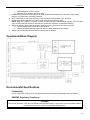
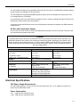
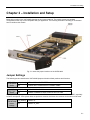
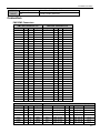
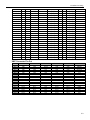
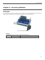
XVPX-9400 Single-Slot 3U VPX bus 8-Channel RAID Controller and PMC/XMC Carrier Module USER’S MANUAL ACROMAG INCORPORATED Tel: (248) 295-0885 30765 South Wixom Road Fax: (248) 624-9234 P.O. BOX 437 Email: [email protected] Wixom, MI 48393-7037 U.S.A. Copyright 2013, Acromag, Inc., Printed in the USA. Data and specifications are subject to change without notice. 8500-984F Part Number 309400 Trademark Information Brand or product names are trademarks or registered trademarks of their respective owners. Intel® and Pentium® are registered trademarks and Celeron™ is a trademark of Intel Corporation. Windows®, Windows XP®, and Windows 7® are registered trademarks of Microsoft Corporation in the US and in other countries. Copyright Information This document is copyrighted by Xembedded, LLC (Xembedded) and shall not be reproduced or copied without expressed written authorization from Xembedded. The information contained within this document is subject to change without notice. Xembedded does not guarantee the accuracy of the information. Associated Documents Due to the complexity of some of the parts used on the XVPX-9400, it is not possible to include all of the detailed data on all such devices in this manual. A list of the specifications and data sheets that provide additional information is as follows: VPX Standard, VITA 46.0 – 2007. http://www.vita.com PLX http://www.plx.com WARNING This is a Class A product. In a domestic environment this product may cause radio interference, in which case the user may be required to take adequate measures. Warning for European Users – Electromagnetic Compatibility European Union Directive 89/336/EEC requires that this apparatus comply with relevant ITE EMC standards. EMC compliance demands that this apparatus is installed within a VME enclosure designed to contain electromagnetic radiation and which will provide protection for the apparatus with regard to electromagnetic immunity. This enclosure must be fully shielded. An example of such an enclosure is a Schroff® 7U EMC-RFI VME System chassis, which includes a front cover to complete the enclosure. The connection of non-shielded equipment interface cables to this equipment will invalidate European Free Trade Area (EFTA) EMC compliance and may result in electromagnetic interference and/or susceptibility levels that are in violation of regulations which apply to the legal operation of this device. It is the responsibility of the system integrator and/or user to apply the following directions, as well as those in the user manual, which relate to installation and configuration: All interface cables should be shielded, both inside and outside of the VME enclosure. Braid/foil type shields are recommended for serial, parallel and SCSI interface cables. Where as external mouse cables are not generally shielded, an internal mouse interface cable must either be shielded or looped (1 turn) through a ferrite bead at the enclosure point of exit (bulkhead connector). External cable connectors must be metal with metal back-shells and provide 360-degree protection about the interface wires. The cable shield must be terminated directly to the metal connector shell; shield ground drain wires alone are not adequate. VPX panel mount connectors that provide interface to external cables (e.g., RS232, USB, keyboard, mouse, etc.) must have metal housings and provide direct connection to the metal VPX chassis. Connector ground drain wires are not adequate. Environmental Protection Statement This product has been manufactured to satisfy environmental protection requirements where possible. Many of the components used (structural parts, printed circuit boards, connectors, batteries, etc.) are capable of being recycled. Final disposition of this product after its service life must be accomplished in accordance with applicable country, state, or local laws or regulations. ii Note This VPX 8-Channel RAID Controller and PMC/XMC carrier module is designed to be used in a VPX backplane that supports module profile MOD3-PAY-1D-16.2.6-2. Use of this module in any other backplane profile could result in damage to this module or others in the chassis Technical Support In the unlikely event that you experience problems with your product, contact Technical Support. Please be prepared to provide contact information and details of your problem. You may be asked for further details when calling: TELEPHONE FAX 734-975-0577 734-975-0588 Support may also be obtained via email. E-mail to [email protected] iii Table of Contents Chapter 1 – Introduction ............................................................................................................................................ 1-1 Module Features ....................................................................................................................................................... 1-1 Module and Backplane Profiles ................................................................................................................................ 1-1 Handling .................................................................................................................................................................... 1-1 ESD Safe Work Area Guidelines ........................................................................................................................... 1-1 Operational Block Diagram ....................................................................................................................................... 1-2 Environmental Specifications .................................................................................................................................... 1-2 Flammability .......................................................................................................................................................... 1-2 EMI/EMC Regulatory Compliance ......................................................................................................................... 1-2 I2C Bus and Temperature Sensor ......................................................................................................................... 1-3 Electrical Specifications ............................................................................................................................................ 1-3 VPX Power Supply Requirements ......................................................................................................................... 1-3 Power Consumption .............................................................................................................................................. 1-3 Auxiliary Supply ..................................................................................................................................................... 1-4 Build Levels ........................................................................................................................................................... 1-4 Ordering Information ................................................................................................................................................. 1-4 Chapter 2 – Installation and Setup ............................................................................................................................ 2-1 Jumper Settings ........................................................................................................................................................ 2-1 Connectors ................................................................................................................................................................ 2-2 PMC/XMC Connectors .......................................................................................................................................... 2-2 XMC Connector Pin Out ........................................................................................................................................ 2-3 VPX Connectors .................................................................................................................................................... 2-4 Front Panel Layout .................................................................................................................................................... 2-5 Installation ................................................................................................................................................................. 2-5 Board Keying ......................................................................................................................................................... 2-5 Installation Notes ................................................................................................................................................... 2-5 Power Requirements ............................................................................................................................................. 2-6 Connecting to XVPX-9400 .................................................................................................................................... 2-6 Power-Up/Reset Sequence ................................................................................................................................... 2-6 Chapter 3 – Accessory Modules ............................................................................................................................... 3-1 XVPX-9940................................................................................................................................................................ 3-1 Jumpers ................................................................................................................................................................. 3-1 Connectors ............................................................................................................................................................ 3-2 Chapter 4 Revision History ........................................................................................................................................ 4-1 iv Introduction Chapter 1 – Introduction Xembedded’s XVPX-9400 is a rugged 8-Channel RAID Controller and PMC/XMC Carrier Module in the 3U VPX form factor, targeted for processing, communications and display applications in the commercial, military and aerospace markets. In addition to the RAID controller which provides connection for up to 8 drives, the XVPX-9400 also allows the use of a PMC or XMC module. The XVPX-9940 is the Rear Transition Module for the XVPX-9400 used to turn the backplane I/O into standard SATA connections. The XVPX-9400 supports up to eight PCI Express lanes from the backplane for connection to other cards in the system. Module Features 8-Channel RAID controller with Heartbeat monitor The PMC site is 64-bit, 133MHz 3.3VIO The XMC site is PCIe 8-lanes Gen 2.0 Supports standard IEEE1386.1 modules Supports Vita 65, OpenVPX Module conforms to VPX Spec. Vita 46.0, 46.4 and 46.9 Front panel I/O for the Air-cooled versions. Rear I/O for all differential I/O lines for all variants 8 lanes of PCI Express (Vita 46.0 and 46.4) 3U VPX form factor supporting OpenVPX and Vita 65 Air and conduction-cooled variants REDI covers supporting Vita 48 is available Module and Backplane Profiles The XVPX-9400 conforms to module profile MOD3-PAY-1D-16.2.6-2. Use of this module in an incompatible backplane profile could result in damage to this module or others in the chassis. Note Due to a BIOS limitation on the XVPX-6300, when used with this CPU module the XVPX-9400 RAID device or installed PMC/XMC card may not boot properly when connected to Fat Pipe B. They will function normally from inside an operating system. These devices will boot normally if connected to Fat Pipe A. Handling Modules should be handled in ESD-safe work areas in order to prevent damage to sensitive components from electrostatic discharges. These areas must be designed and maintained to prevent ESD damage. ESD Safe Work Area Guidelines 1. Module should be handled at properly designated work areas only. 2. Designated ESD safe work areas must be checked periodically to ensure their continued safety from ESD. The areas should be monitored for the following: a. Proper grounding methods. b. Static dissipation of work surfaces. 1-1 Introduction 3. 4. 5. 6. 7. c. Static dissipation of floor surfaces. d. Operation of ion blowers and ion air guns. Designated work areas must be kept free of static generating materials such as styrofoam, vinyl, plastic, fabrics or any other static generating materials. Work areas must be kept clean and neat in order to prevent contamination of the work area. Modules should be handled by the edges. Avoid touching the component leads. NOTE: When not installed in a system, modules must be enclosed in shielded bags or boxes. There are three types of ESD protective enclosure materials this module was shipped in an approved ESD bag. Whenever handling the module the operator must be properly grounded by one of the following: a. Wearing a wrist strap connected to earth ground. b. Wearing heel grounders and have both feet on a static dissipative floor surface. Stacking of modules should be avoided to prevent physical damage. Operational Block Diagram Environmental Specifications Flammability The circuit board is made by an UL recognized manufacturer and has a flammability rating of UL94V-1. EMI/EMC Regulatory Compliance Caution This module generates, uses, and can radiate electromagnetic energy. It may cause, or be susceptible to EMI if not installed and used in a cabinet with adequate EMI protection. 1-2 Introduction The XVPX-9400 is designed using good EMC practices and, when used in a suitably EMC‐compliant chassis, should maintain the compliance of the total system. The XVPX-9400 also complies with EN60950 (product safety), which is essentially the requirement for the Low Voltage Directive (73/23/EEC). Air-cooled build levels of the XVPX-9400 are designed for use in systems meeting VDE class B, EN and FCC regulations for EMC emissions and susceptibility. Conduction-cooled and REDI build levels of the XVPX-9400 are intended for integration into EMC hardened cabinets/boxes. I2C Bus and Temperature Sensor There is one I2C bus to access the FRU (Field Replaceable Unit) which can store user data. This device will also report board temperature and status. Caution The XVPX-9400 requires air-flow of at least 200 LFM for the air-cooled version plus what is required for the PMC/XMC installed on this module. If the conduction-cooled XVPX-9400 is operating on an extender card, it requires air-flow of at least 300 LFM across it. Versions using the REDI covers MUST NOT operate outside of a fully configured and fully installed conduction-cooled REDI system. With the covers installed conduction is the only cooling method. ENVIRONMENTAL SPECIFICATION THERMAL Air-cooled Conduction-cooled REDI Cover, Conduction-cooled HUMIDITY SHOCK VIBRATION 20 - 2000 Hz COMPLIANCE FORM FACTOR * w/ 200lfm airflow 1 OPERATING NON-OPERATING 0° to 70°C* -40° to 85°C*1 -40° to 85°C*2 20% - 80% RH, non-condensing 30 g peak acceleration, 11msec duration .015” (.38mm) peak-to-peak displacement 2.5 g max acceleration IEEE 1386.1 (CMC Standard), Vita 46.0, 46.4, 46.9, 48 and 65 MIL Spec 217-F@ 105,000 Hrs 6.299” (160mm), 3.937” (100mm) must operate in a fully installed conduction-cooled rack 2 -40° to 85°C -40° to 105°C -40° to 105°C 50 g peak acceleration, 11msec duration .030” (.76mm) peak-to-peak displacement 5.0 g max acceleration must operate in a fully installed conduction-cooled RAID rack Electrical Specifications VPX Power Supply Requirements The XVPX-9400 requires +3.3V and +5V from the VPX back plane. The +/-12V supplies are used only if required by the PMC/XMC module. Power Consumption +5V: 48W max (w/o mezzanine card) +3.3V: 20W max (w/o mezzanine card) 1-3 Introduction Auxiliary Supply The following functions may be powered from the 3.3 V Auxiliary supply (VPX +3.3V_AUX line): FRU EEPROM, TEMP SENSOR Build Levels The XVPX-9400 is available in three electrically compatible build levels, each of which is carefully tailored to a particular set of requirements and environments. All three levels fully support the power and versatility of VPX, so no matter how large or diversified your project, absolute compatibility is assured at all stages of development. The three build levels have three basic mechanical configurations, both in accordance with the VITA 46.0 VPX standard and the Vita 48 REDI standard: 1. Air (convection) cooled modules are intended for use in standard industrial chassis. 2. Conduction-cooled modules are intended for use in sealed Air Transportable Racking (ATR) and other conduction-cooled environments. 3. REDI cover, Conduction-cooled modules are intended for use in sealed Air Transportable Racking (ATR) and other conduction-cooled environments. Ordering Information XVPX-9400-A00-X A = CPU X = SOLDER 1 = Air-cooled 2 = Conduction-cooled 3 = REDI Conduction-cooled LF – Lead-free solder 1-4 Installation and Setup Chapter 2 – Installation and Setup Below is the outline of the XVPX-9400 showing the six jumper locations. The module comes in a standard configuration which may not be compatible with your application. The following information will help you understand how to configure this module. Fig. 2-1 shows the jumper locations on the XVPX-9400 Jumper Settings The following section describes the XVPX-9400 jumpers with their default positions and functions. PEXSPD PCIe Speed Select 1-2 (default) GEN 1 & GEN 2 SUPPORTED 2-3 FORCE GEN 1 SPEED ON ALL CONNECTIONS CLKSEL 1-2 (default) NON-COMMON CLOCK PCIe Clock 2-3 100MHz COMMON CLOCK FROM P0 REFCLK PINS Select Best system stability may be achieved with the use of a 100MHz common clock connection from the SBC, especially at Gen 2 link speeds. If the system does not provide a common clock then non-common clock mode must be used. FRUSEL FRU & Temp Sensor Voltage 1-2 (default) USES 3.3V 2-3 USES 3.3V_AUX 2-1 Installation and Setup ORBGND Orb/Chassis Ground 1-2 (default) FRONT PANEL TIED TO GND 2-3 FRONT PANEL ISOLATED Connectors PMC/XMC Connectors PMC Site Connector J11 PMC Site Connector J12 Signal PIN PIN Signal Signal PIN PIN Signal TCK 1 2 -12V +12V 1 2 TRST* Ground 3 4 INTA* TMS 3 4 TDO INTB* 5 6 INTC* TDI 5 6 Ground BUSMODE1* 7 8 +5V Ground 7 8 PCI-RSVD* PCI-RSVD* INTD* 9 10 PCI-RSVD* PCI-RSVD* 9 10 Ground 11 12 PCI-RSVD* BUSMODE2* 11 12 +3.3V CLK 13 14 Ground RST* 13 14 BUSMODE3* Ground 15 16 GNT* +3.3V 15 16 BUSMODE4* REQ* 17 18 +5V PCI-RSVD* 17 18 Ground V(I/O) 19 20 AD(31) AD(30) 19 20 AD(29) AD(28 21 22 AD(27) Ground 21 22 AD(26) AD(25) 23 24 Ground AD(24) 23 24 +3.3V Ground 25 26 C/BE(3)* IDSEL 25 26 AD(23) AD(22) 27 28 AD(21) +3.3V 27 28 AD(20) AD(19) 29 30 +5V AD(18) 29 30 Ground V(I/O) 31 32 AD(17) AD(16) 31 32 C/BE(2)* FRAME* 33 34 Ground Ground 33 34 PMC-RSVD Ground 35 36 IRDY* TRDY* 35 36 +3.3V DEVSEL* 37 38 +5V Ground 37 38 STOP* Ground 39 40 LOCK* PERR* 39 40 Ground SDONE* 41 42 SBO* +3.3V 41 42 SERR* PAR 43 44 Ground C/BE(1)* 43 44 Ground V(I/O) 45 46 AD(15) AD(14) 45 46 AD(13) AD(12) 47 48 AD(11) M66EN 47 48 AD(10) AD(09) 49 50 +5V AD(08) 49 50 +3.3V Ground 51 52 C/BE(0)* AD(07) 51 52 PMC-RSVD AD(06) 53 54 AD(05) +3.3V 53 54 PMC-RSVD AD(04) 55 56 Ground PMC-RSVD 55 56 Ground V(I/O) 57 58 AD(03) PMC-RSVD 57 58 PMC-RSVD AD(02) 59 60 AD(01) Ground 59 60 PMC-RSVD AD(00) 61 62 +5V ACK64* 61 62 +3.3V Ground 63 64 REQ64* Ground 63 64 PMC-RSVD PMC Site Connector J13 Signal PIN PIN PCI-RSVD 1 Ground 3 C/BE(6)* 5 C/BE(4)* V(I/O) PMC Site Connector J14 (shown as differential pairs) Signal Pair Number Signal PIN PIN Signal Pair Number 2 Ground Pair 1 PMC_IO1_DN 1 2 PMC_IO2_DN Pair 2 4 C/BE(7)* Pair 1 PMC_IO1_DP 3 4 PMC_IO2_DP Pair 2 6 C/BE(5)* Pair 3 PMC_IO3_DN 5 6 PMC_IO4_DN Pair 4 7 8 Ground Pair 3 PMC_IO3_DP 7 8 PMC_IO4_DP Pair 4 9 10 PAR64 Pair 5 PMC_IO5_DN 9 10 PMC_IO6_DN Pair 6 AD(63) 11 12 AD(62) Pair 5 PMC_IO5_DP 11 12 PMC_IO6_DP Pair 6 AD(61) 13 14 Ground Pair 7 PMC_IO7_DN 13 14 PMC_IO8_DN Pair 8 2-2 Installation and Setup Ground 15 16 AD(60) Pair 7 PMC_IO7_DP 15 16 PMC_IO8_DP Pair 8 AD(59) 17 18 AD(58) Pair 9 PMC_IO9_DN 17 18 PMC_IO10_DN Pair 10 AD(57) 19 20 Ground Pair 9 PMC_IO9_DP 19 20 PMC_IO10_DP Pair 10 V(I/O) 21 22 AD(56) Pair 11 PMC_IO11_DN 21 22 PMC_IO12_DN Pair 12 AD(55) 23 24 AD(54) Pair 11 PMC_IO11_DP 23 24 PMC_IO12_DP Pair 12 AD(53) 25 26 Ground Pair 13 PMC_IO13_DN 25 26 PMC_IO14_DN Pair 14 Ground 27 28 AD(52) Pair 13 PMC_IO13_DP 27 28 PMC_IO14_DP Pair 14 AD(51) 29 30 AD(50) Pair 15 PMC_IO15_DN 29 30 PMC_IO16_DN Pair 16 AD(49) 31 32 Ground Pair 15 PMC_IO15_DP 31 32 PMC_IO16_DP Pair 16 Ground 33 34 AD(48) Pair 17 PMC_IO17_DN 33 34 PMC_IO18_DN Pair 18 AD(47) 35 36 AD(46) Pair 17 PMC_IO17_DP 35 36 PMC_IO18_DP Pair 18 AD(45) 37 38 Ground Pair 19 PMC_IO19_DN 37 38 PMC_IO20_DN Pair 20 V(I/O) 39 40 AD(44) Pair 19 PMC_IO19_DP 39 40 PMC_IO20_DP Pair 20 AD(43) 41 42 AD(42) Pair 21 PMC_IO21_DN 41 42 PMC_IO22_DN Pair 22 AD(41) 43 44 Ground Pair 21 PMC_IO21_DP 43 44 PMC_IO22_DP Pair 22 Ground 45 46 AD(40) Pair 23 PMC_IO23_DN 45 46 PMC_IO24_DN Pair 24 AD(39) 47 48 AD(38) Pair 23 PMC_IO23_DP 47 48 PMC_IO24_DP Pair 24 AD(37) 49 50 Ground Pair 25 PMC_IO25_DN 49 50 PMC_IO26_DN Pair 26 Ground 51 52 AD(36) Pair 25 PMC_IO25_DP 51 52 PMC_IO26_DP Pair 26 AD(35) 53 54 AD(34) Pair 27 PMC_IO27_DN 53 54 PMC_IO28_DN Pair 28 AD(33) 55 56 Ground Pair 27 PMC_IO27_DP 55 56 PMC_IO28_DP Pair 28 V(I/O) 57 58 AD(32) Pair 29 PMC_IO29_DN 57 58 PMC_IO30_DN Pair 30 PCI-RSVD 59 60 PCI_RSVD Pair 29 PMC_IO29_DP 59 60 PMC_IO30_DP Pair 30 PCI-RSVD 61 62 Ground Pair 31 PMC_IO31_DN 61 62 PMC_IO32_DN Pair 32 Ground 63 64 PCI-RSVD Pair 31 PMC_IO31_DP 63 64 PMC_IO32_DP Pair 32 XMC Connector Pin Out 01 02 03 04 05 06 07 08 09 10 11 12 13 14 15 16 17 18 19 A DP00+ GND DP02+ GND DP04+ GND DP06+ GND DP08+ GND DP10+ GND DP12+ GND DP14+ GND DP16+ GND DP18+ B DP00GND DP02GND DP04GND DP06GND DP08GND DP10GND DP12GND DP14GND DP16GND DP18- C 3.3V TRST# 3.3V TCK 3.3V TMS 3.3V TDI RPS TDO MBIST# GA1 3.3V AUX GZ2 RPS MVMRO RFU RPS RPS D DP01+ GND DP03+ GND DP05+ GND DP07+ GND DP09+ GND DP11+ GND DP13+ GND DP15+ GND DP17+ GND DP19+ E DP01GND DP03GND DP05GND DP07GND DP09GND DP11GND DP13GND DP15GND DP17GND DP19- F VPWR MRSTI# VPWR MRSTO# VPWR +12V VPWR -12V VPWR GA0 VPWR MPRESENT# VPWR MSDA VPWR MSCL RFU RPS RPS 2-3 Installation and Setup VPX Connectors P0 Connector P0 Wafer 1 A +3.3 V B +3.3 V C +3.3 V D None E +12 V F Unused G +12 V 2 +3.3 V +3.3 V +3.3 V None +12 V +12 V +12 V 3 +5 V +5 V +5 V None +5 V +5 V +5 V 4 NVRMO SYSRESET- GND -12V GND UNUSED UNUSED 5 SM1 SM0 GND +3V3_AUX GND GA4- GAP- 6 GA0 GA1 GND UNUSED GND GA2- GA3- 7 TRST TMS GND TDI TDO GND TCLK 8 GND UNUSED UNUSED GND UNUSED UNUSED GND P1 Connector P1 Wafer A B C D E 1 PCIE_RXP0 2 GND 3 PCIE_RXP2 F G PCIE_RXN0 GND PCIE_TXP0 PCIE_RXP1 PCIE_RXN1 GND PCIE_TXN0 GND UNUSED PCIE_TXP1 PCIE_TXN1 PCIE_RXN2 GND PCIE_TXP2 GND PCIE_TXN2 GND UNUSED 4 GND PCIE_RXP3 PCIE_RXN3 GND PCIE_TXP3 PCIE_TXN3 GND 5 PCIE_RXP4 PCIE_RXN4 GND PCIE_TXP4 PCIE_TXN4 GND UNUSED 6 GND PCIE_RXP5 PCIE_RXN5 GND PCIE_TXP5 PCIE_TXN5 GND 7 PCIE_RXP6 PCIE_RXN6 GND PCIE_TXP6 PCIE_TXN6 GND UNUSED 8 GND PCIE_RXP7 PCIE_RXN7 GND PCIE_TXP7 PCIE_TXN7 GND 9 SATA_RXP0 SATA_RXN0 GND SATA_TXP0 SATA_TXN0 GND ZEROIZE_LED 10 GND SATA_RXP1 SATA_RXN1 GND SATA_TXP1 SATA_TXN1 GND 11 SATA_RXP2 SATA_RXN2 GND SATA_TXP2 SATA_TXN2 GND PURGE# 12 GND SATA_RXP3 SATA_RXN3 GND SATA_TXP3 SATA_TXN3 GND 13 SATA_RXP4 SATA_RXN4 GND SATA_TXP4 SATA_TXN4 GND ZEROIZE# 14 GND SATA_RXP5 SATA_RXN5 GND SATA_TXP5 SATA_TXN5 GND 15 SATA_RXP6 SATA_RXN6 GND SATA_TXP6 SATA_TXN6 GND UNUSED 16 GND SATA_RXP7 SATA_RXN7 GND SATA_TXP7 SATA_TXN7 GND B PMCIO2_DN C GND P2 Connector P2 Wafer 1 A PMCIO2_DP D PMCIO1_DP E PMCIO1_DN F GND G UNUSED 2 GND PMCIO4_DP PMCIO4_DN GND PMCIO3_DP PMCIO3_DN GND 3 PMCIO6_DP PMCIO6_DN GND PMCIO5_DP PMCIO5_DN GND UNUSED 4 GND PMCIO8_DP PMCIO8_DN GND PMCIO7_DP PMCIO7_DN GND 5 PMCIO10_DP PMCIO10_DN GND PMCIO9_DP PMCIO9_DN GND UNUSED 6 GND PMCIO12_DP PMCIO12_DN GND PMCIO11_DP PMCIO11_DN GND 7 PMCIO14_DP PMCIO14_DN GND PMCIO13_DP PMCIO13_DN GND UNUSED 8 GND PMCIO16_DP PMCIO16_DN GND PMCIO15_DP PMCIO15_DN GND 9 PMCIO18_DP PMCIO18_DN GND PMCIO17_DP PMCIO17_DN GND UNUSED 10 GND PMCIO20_DP PMCIO20_DN GND PMCIO19_DP PMCIO19_DN GND 11 PMCIO22_DP PMCIO22_DN GND PMCIO21_DP PMCIO21_DN GND UNUSED 12 GND PMCIO24_DP PMCIO24_DN GND PMCIO23_DP PMCIO23_DN GND 13 PMCIO26_DP PMCIO26_DN GND PMCIO25_DP PMCIO25_DN GND UNUSED 14 GND PMCIO28_DP PMCIO28_DN GND PMCIO27_DP PMCIO27_DN GND 15 PMCIO30_DP PMCIO30_DN GND PMCIO29_DP PMCIO29_DN GND UNUSED 16 GND PMCIO32_DP PMCIO32_DN GND PMCIO31_DP PMCIO31_DN GND 2-4 Installation and Setup Front Panel Layout The XVPX-9400 uses four onboard LEDs to indicate the status of PCIe link training. The VPX_PG (VPX back plane to the system processor), 8114PG (PCIe link train to the PMC sites), XMC_PG (XMC link train to the XMC site), and RAIDPG (PCIe link train to the LSI RAID Controller) may be solid or blinking if these items are linked. On the front panel of air-cooled assemblies, there are 8 activity LEDs, one for each drive connection. These LEDs indicate activity to the drive. There is also a blue heartbeat LED, which blinks indicating that the firmware is running properly on the LSI RAID Controller. Fig. 3-1 shows an air-cooled front panel Installation The XVPX-9400 VPX bus carrier can connect to the VPX bus as a Double Fat Pipe (PCIe x8) device, but is also supported with a smaller link width. The path to the XMC site is PCIe x8 from the PCIe switch. The PMC site is PCIx 133MHz 64-bit interface and only supports 3.3V signaling. The PMC/XMC rear I/O is out the P14 connector, consult the VPX P2 connector for the pin out of this I/O, Vita 46.9 standard was followed on this design. Review the Safety Notices section before installing the board. The following notices also apply: Caution The XVPX-9400 has been specifically designed for use with 3U VPX backplanes and may not be compatible with some 6U backplanes. Plugging the board into an unsupported 6U VPX backplane may cause permanent component damage. Consult the enclosure documentation to ensure that the XVPX-9400’s power requirements are compatible with those supplied by the backplane. Board Keying The 3U VPX backplane specification requires all backplane slots to have two guide pins: one above the J0 connector and one below the J2 connector. As well as providing correct alignment, these pins are keyed to prevent cards from being inserted into incorrect backplane slot(s) to avoid electrical incompatibility. The XVPX-9400 has receptacles for these guide pins (see the Connectors section). By default, these are not keyed. Please contact the factory to discuss keying requirements. Installation Notes 1. Keying may dictate the backplane slot(s) into which the XVPX-9425 can be inserted. 2. Air-cooled versions have an ejector handle to ensure that the backplane connectors mate properly with the backplane. The captive screws at the top and bottom of the front panel allow the XVPX-9425 to be tightly secured in position, which provides continuity with system chassis ground. 3. Conduction-cooled and REDI versions have screw driven wedge locks at the top and bottom of the board to provide the necessary mechanical/thermal interface. Correct adjustment requires a calibrated torque wrench set to between 0.6 and 0.8 Nm. 2-5 Installation and Setup 4. In an air-cooled development enclosure, when making I/O connections from the backplane connectors, use of Xembedded’s RTM modules (or some equivalent system) ensures optimum operation with regard to EMI. Power Requirements The XVPX-9400 may require up to 6 Amps from the +3.3V supply and up to 9.6 Amps from the +5V supply. For more details, see the Electrical Specification in Chapter 1. Connecting to XVPX-9400 One single width PMC/XMC module can be fitted to the XVPX-9400, which is set to 3.3V signaling only. The XVPX-9425 does not support 5V signaling and may cause damage to the PMC/XMC module if connected. It is usually necessary to install driver software to the system to support the PMC/XMC module. Consult the PMC/XMC manufacturer’s manual for this information. To install a PMC/XMC module first slid the front bezel of the module thru the XVPX-9400 (only if air-cooled version). Then press down to join the PMC/XMC connectors to the XVPX-9400 as shown below. Power-Up/Reset Sequence From the application of 3.3V and 5V power to all components being out of reset typically takes 250 ms. Since the ramp up times of the 3.3V and 5V system power source and the onboard power source will vary with load, the time taken for the XVPX-9400 to come out of reset will vary from system to system. It is the software’s responsibility to account for this. 2-6 Accessory Modules Chapter 3 – Accessory Modules XVPX-9940 The XVPX-9940 is the rear transition module for the XVPX-9400 and is used in backplanes that bring out the rear I/O signals from the XVPX-9400. If you are using a custom backplane you will not need the RTM. Fig. 4-1 shows the XVPX-9940 Jumpers The XVPX-9940 only has one jumper setting, ORB (front panel) ground: ORBGND 1-2 (default) ORB GND TIED TO DIGITAL GND 2-3 ORB GND ISOLATED 3-1 Accessory Modules Connectors This section provides pin outs for some of the XVME-9940 connectors. Refer to the EMC warning at the beginning of this manual before attaching cables. Purge Purge input to the XVPX-9400: 1 2 3 Purge N/C GND Zeroize Zeroize input to the XVPX-9400: 1 2 3 Zero N/C GND J_0LED This is the Zeroize function LED. Connect the external LED from Pin-1 to a limit resistor to LED and Pin-3 to GND for LED. This provides an external indication that a Zeroize cycle has started and is in progress. 1 Zero LED 2 N/C 3 GND 3-2 Revision History Chapter 4 Revision History The following table shows the revision history for this document: Release Date Revision EGR/DOC Description of Revision JUN-10 A JAS Initial Release SEP-11 B JAS Edits MAR-12 C DWR Updated for new PCB artwork; numerous edits SEP-12 C1 (D) DWR Added warning about option ROM usage on FAT PIPE B. 29-OCT-13 E DWR Corrected P1 pin out table 2-Oct-15 F CAB/MJO Remove Lead Solder Option for RoHS Compliance. 4-1