1
DMs200
User'sManual
ffi
Inc.
RealTimeDevices,
"AccessingtheAnalog World'*
ISO9001 and AS9100 Certified
(Read/Write)
BA + 6: 8254Timer/Counter2
(Write
Only)...........
BA + 7: 8254ControlWord
(Read/Write)
...............
12-BitConversion
BA + 8: ReadMSB Data/Start
(Read/Write)
................
8-BitConversion
BA + 9: ReadLSB Data/Start
IRQ (Read/Write)
BA + 10: ReadStatus/Clear
BA + 11: IRQ Enable(WriteOnly)...........
andSettingBitsin a Port...........
Clearing
EnablingandDisablingInterrupts
StartinganA./DConversion
...............4-6
'.'......4-6
............4-7
...'..........4-7
............4-7
....'........'.....4-7
....'.'.....'.'.......4-8
......4-lO
................4-10
Status..........
MonitoringConversion
Data............
ReadingtheConverted
....'..................4-11
'..4-lI
IntenuptController
8259Programmable
(IMR) ..........
MaskRegister
Interrupt
End-of-Intemrpt(EOI) Command
WhenanInterruptOccurs?
WhatExactlyHappens
UsingIntemrptsin Your Programs
Routine(ISR)............
WritinganIntemrptService
Savingthe StartupInterruptMaskRegister(IMR) andInterruptVector
Restoringthe StartupIMR andInterruptVector
CommonInterruptMistakes
.................4-13
......................4-13
......4-13
.....................4-13
.....4-13
......................4-13
..........4-15
.....4-15
...............4-15
andFlow Diagrams
ExamplePrograms
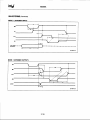
SingleConvertFlowDiagram(Figure4-3)..............
FlowDiagram(Figure4-4)..............
Scanning
Channel
CHAPTER 5 _ CALIBRATION
APPENDX A _ DMs2OOSPECIFICATIONS
APPENDD(B _P2 CONNECTORPIN ASSIGNMENTS
APPENDIX C - COMPONENT DATA SITEETS
APPENDX D _ WARRANTY
...'.'4-18
....................4-19
...............4-20
5.1
.......A-1
......B.1
c.1
D-1
List of lllustrations
1-1
t-2
1-3
t-4
1-5
1-6
t-7
1-8
r-9
1-10
1-11
r-t2
1-13
2-l
aa
3-1
4-l
4-2
4-3
4-4
5-1
...................
Settings
ModuleLayoutShowingFactory-Configured
Jumper,
P3
................
IntemrptChannel
Request
Line .............
PullingDowntheInterrupt
Jumpers,
P4................
ClockSource
8254Timer/Counter
CircuitBlockDiagram
S254TimerlCounter
P5andP6................
AnalogInputVoltageRangeandPolarity,
P7 ...............
Jumper,
Source
Interrupt
PortB, Bits4-7Pads,P8
Switch,
51 ................
BaseAddress
for the8255.............
Resistors
Pull-up/Pull-down
to DigitalVO Lines
AddingPull-upsandPull-downs
for Calculating
Gx andf ............
GainCircuitryandFormulas
Short
Solder
............
Diagramfor Removalof
.............
PinAssignments
P2UOConnector
............
AnalogInputConnections
DM5200BlockDiagram..................
TimingDiagrarn.......
A/D Conversion
IntervalTimer CircuitBlock Diagram
8254Programmable
FlowDiagram
SingleConversion
Scanning
FlowDiagram
Channel
DM5200ModuleLavout
u,
...............1-3
...............
1-4
.....................
1-4
1-5
........
........1-5
....................1-6
1-6
..................
.......'..........1-6
......................1-7
.....................1-8
...............1-9
....................1-10
....1-10
.........2-4
........................2-5
.....................3-3
................4-11
...4-16
.......................4-19
.......................4-20
.................5-3
INTRODUCTION
The DM5200 dataModule@medium speedanalog input module turns your IBM PC-compatible cpuModulerM or
other PC/104 computer into a high-performancedata acquisition and control system.Ultra-compact for embedded
and portable applications, the DM5200 features:
.
.
.
.
.
.
.
.
16 single-endedanalog input channels,
I2-bit,20 microsecond A/D converter,
t5, +10, or 0 to +10 volt analoginput range,
Resistor configurable gain,
20 TTL/CMOS 8255 basedprogrammabledigital VO (16 at VO connector,4 at on-board pads),
Three independent 16-bit, 8-MHz timer/counters,
+5 volt only operation,
BASIC, Turbo Pascal,and Turbo C sourcecode; diagnosticsprogram.
The following paragraphsbriefly describethe major functions of the module. More detailed discussionsof
module functions are included in Chapter 3, Hardware Description, and Chapter 4, Module Operation and Programming. The module setup is describedin Chapter l, Module Settings.
Analog-to-Digital Conversion
The analog-to-digital (A/D) circuitry receivesup to 16 single-endedanalog inputs and converts these inputs into
12-bit digital data words which can then be read and/or transferredto PC memory.
The analog input voltage range is jumper-selectablefor bipolar rangesof -5 to +5 volts or -10 to +10 volts, or a
unipolar range of 0 to +10 volts. The module is factory set for -5 to +5 volts. Overvoltage protection to +35 volts is
provided at the inputs. A./D conversionsare performed by a l2-bit successiveapproximation converter. This highperformance converter and the high-speedsample-and-holdamplifier preceding it make sure that dynamic input
voltages are accurately digitized. The resolution of a 12-bit conversion is 2.4414 millivolts and the maximum
throughput is 40,000 samplesper second.
The converted data is read and/or transferredto PC memory, one byte at a time, through the PC data bus.
8254Timer/Counter
An 8254 programmable interval timer contains three l6-bit, 8-MHz timer/countersto support a wide range of
timing and counting functions. The clock, gate and output pins for each of the three timer/counters are available at
the VO connector.
Digital UO
The DM5200 has 20 TTL/CMOS-compatible digital VO lines which can be directly interfaced with external
devices or signals to senseswitch closures,trigger digital events,or activate solid-staterelays. The lines are provided by the on-board 8255 programmableperipheral interface (PPI) chip. Sixteen of the lines are brought out to the
VO connector and four are available at a set of on-board pads located near the edge of the module for easy access.
Pads for installing and activating pull-up or pull-down resistorsare included on the module for the 16 lines brought
out to the VO connector.Installation proceduresare given at the end of Chapter l, Module Settings.
What ComesWith Your Module
You receive the following items in your DM5200 package:
.
.
.
.
DM5200 interface module with stackthroughbus header
Mounting hardware
Software and diagnosticsdiskette with example programs in BASIC, Turbo Pascal,and Turbo C; source code
IJser's manual
If any item is missing or damaged,pleasecall Real Time Devices' Customer Service Department at
(814) 234-8087. If you require service outside the U.S., contact your local distributor.
i-3
Module Accessories
In addition to the items included in your module package,Real Time Devices offers a full line of software and
hardware accessories.Call your local distributor or our main office for more information about these accessoriesand
for help in choosing the best items to support your module's application.
Application Software and Drivers
Our custom application software packagesprovide excellent data acquisition and analysis support. Use
SIGNAL*VIEWTM for real-time monitoring and data acquisition, and SIGNAL*MATHTM for integrated data
acquisition and sophisticateddigital signal processingand analysis.rtdlinxrM and rtdlinx/NB drivers provide
full-featured high level interfacesbetween the DM5200 and custom or third party software, including Labtech
Notebook, Notebook/XE, and LTlControl. rtdlinx sourcecode is available for a one-time nominal fee.
Hardware Accessories
Hardware accessoriesfor the DM5200 include the MX32 analog input expansionboard which can expand a
single input channel on your module to 16 differential or 32 single-endedinput channels,the OP seriesoptoisolated
digital input boards,the MR seriesmechanicalrelay output boards,the OR16 optoisolateddigital inpuVmechanical
relay output board, the TS16 thermocouple sensorboard, the TB50 terminal board and XB50 prototype/terminal
board for easy signal accessand prototype development,the DM14 extenderboard for testing your module in a
conventional desktop computer, and XP50 flat ribbon cable assemblyfor external interfacing.
Optional Configurations
Other configurations of the DM5200 are available, such as vertical connectorson some or all VO connectors,a
right angle or other type of connector for easy use of the four digital VO lines brought out to pads, or a nonstackthroughbus connector.If you need an optional configuration for your requirements,pleaseconsult the factory.
Using This Manual
This manual is intended to help you install your new module and get it running quickly, while also providing
enough detail about the module and its functions so that you can enjoy maximum use of its featureseven in the most
complex applications. We assumethat you already have an understandingof data acquisition principles and that you
can customize the example software or write your own applicationsprograms.
When You Need Help
This manual and the example programs in the software packageincluded with your module provide enough
information to properly use all of the module's features.If you have any problems installing or using this module,
contact our Technical Support Department, (814) 234-8087, during regular businesshours, easternstandardtime or
easterndaylight time, or send a FAX requestingassistanceto (814) 234-5218.When sending a FAX request,please
include your company's name and address,your n€rme,your telephonenumber, and a brief description of the
problem.
i-4
CHAPTER 1
MODULE SETTINGS
The DM5200 hasjumper and switch settingsyou can changeif
necessaryfor your application.The module is factory-configured
with the settingslisted in Table 1-1 and shown on the module
diagram at the beginning ofthis chapter.Should you needto
changethesesettings,use theseeasy-to-follow instructionsbefore
you install the module in your system.
By installing resistor packs and solderingjumpers in the desired locations in the associatedpads as describednear the end of
the chapter,you can configure 16 of your digital VO lines to be
pulled up or pulled down.
The final sectiondescribeshow to install two resistorsand a
trimpot to set the resistor configurable gain to the value required
for your application. A pad for installing a capacitoris also included in the gain circuitry for creating a low-passfilter.
1-1
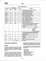
Factory-ConfiguredSwitch and Jumper Settings
jumpersandswitchon the DM5200.Figure 1-1
Table 1-1lists the factorysettingsof the user-configurable
jumpers.
Thefollowingparagraphs
explainhow to
showsthemodulelayoutandthe locationsof thefactory-set
changethe factorysettings.Payspecialattentionto the settingof 51, thebaseaddressswitch,to avoidaddress
contentionwhenyou first useyour modulein your system.
Table1-1- FactorySettings
Switch/
Jumper
FactorySettings
(JumpersInstalled)
P4
FunctionControlled
channel;pullstri-state
Selectsthe activeinterrupt
bufferto ground(G)for multipleinterrupt
applications
Setstheclocksourcesfor the8254
(TCO-TC2)
timer/counters
on CLK0-OSC,
Jumpersinstalled
(cascaded)
CLK1-OT0
& CLK2-OT1
P5
Sets the analog inputvoltagerange
10v
P6
P8
+lSetstheanaloginputvoltagepolarity
Selectsoneof threesignalsas the interrupt
or2
source
installed
8255PortB, bits4-7,padsfor userconnections Noconnections
S1
Setsthe baseaddress
P3
P7
jumper
lnterruplchannelsdisabled;
(ground
installed
on G
for buffer)
300 hex (768 decimal)
fficq*
Fig.1-1- ModuleLayoutShowingFactory-Configured
Settings
l-3
P3 -
Interrupt Channet Select (Factory Setting: Interrupt Channels Disabled; G Connected)
This headerconnector, shown in Figure l-2, lets you connect any one ofthe three interrupt sourceson P7 to an
intemrpt channel, IRQ2 (highest priority channel) through IRQT (lowest priority channel). IRQ2 is the righttmost
channel and IRQT is the leftmost channel (next to last pair of pins). To activate a channel, you must install a jumper
vertically acrossthe desired IRQ channel's pair of pins. Figure 1-2a shows the factory setting; Figure 1-2b shows the
intemrpt source connectedto IRQ3.
!
g)
?I o o o o o .
oooaaH
aoooooo
t
o
o{cDsrsg)N
!
G'
?t l o o o o ? o
u
o
o{g)(rtSqtN
Source
Fig.1-2b:Interrupt
to lRQ3
Connected
Fig.1-2a:
Factory Setting
P3
Fig.1-2- Interrupt
ChannelJumper,
When jumpered, the leftmost pair of pins on P3, labeled G, connectsa 1 kilohm pull-down resistor to the output
of a high-impedance tri-state driver which carries the intemrpt requestsignal. This pull-down resistor drives the
interrupt requestline low whenever intemrpts are not active. Whenever an intemrpt requestis made, the tri-state
buffer is enabled,forcing the output high and generatingan intemrpt. You can monitor the intemtpt statusthrough
bit 1 in the statusword (VO addresslocation BA + 10). After the intemrpt has been serviced,the reset command
returns the IRQ line low, disabling the tri-state buffer, and pulling the output low again. Figure 1-3 shows this
circuit. Becausethe intem-rptrequestline is driven low only by the pull-down resistor, you can have two or more
modules which sharethe sameIRQ channel. You can tell which module issued the intemrpt requestby monitoring
each module's IRQ statusbit.
NOTE: When you use multiple modules that sharethe sameintemrpt, only one module should have the G
jumper installed. The rest should be disconnected.Whenever you operatea single module, the G jumper should be
installed.
E X TI N T
IRQ STATUS
CLK
INTERRUPT
REGISTER
INTERRUPT
Fig.1-3- PullingDownthe Interrupt
RequestLine
t-4
P4 -8254
Timer/Counter Clock Sources (Factory Settings: CLKO-OSC, CLKL-OT0' CLK2'OT1)
This header connector, shown in Figure 1-4, lets you selectthe clock sourcesfor the 8254 timerlcounters"TCO,
TCl, and TC2. The factory setting cascadesall three timer/counters,with the clock source for TCO being the onboard 8 MHz oscillator, the output of TCO providing the clock for TCl, and the output of TC 1 providing the clock
for TC2. You can connect any or all of the sourcesto an external clock input through the P2 VO connector, or you
can set TCl and TC2 to be clocked by the 8 MHz oscillator. Figure l-5 shows a block diagram of the timer/counter
circuitry to help you with these connections.
NOTE: When installing jumpers on this header,make sure that only one jumper is installed in each group of
two or three CLK pins.
P4
osc
It
EC0
oT0
o
r
osc
x
EC1
oT1
Hl8
osc
EC2
P4
Fig.1-4-8254 Timer/Counter
ClockSourceJumpers,
5200
I/O CONNECTOR
P2
r - - r r - - r - l
I
|
I
I
82s4
TIMER/
COUNTER
0
CLK
I
I
I
P1
osc{
qt
I
!
-l
d.|1-{8
- |
|
i
GATE
|
I
I
MHz
P r N : ' EXT CLK O
;-{Mr(*s v
I
OUT
.,
","
EXT GATE O
Itc
ouT 0
I
I
TIMER/
COUNTER
I
o-+
CLK
-l
q5 oi-
GATE
P I N4 3 EXT CLK 1
+5V
EXT GATE 'I
T/C OUT 1
OUT
I
I
OT
TIMER/
COUNTER
2
CLK
ecz*+
EXT CLK 2
EXT GATE 2
GATE
"flc oul 2
OUT
Fig.1-5- 8254Timer/Counter
CircuitBlockDiagram
1-5
P5 -
Analog Input Voltage Range (Factory Setting: 10V)
This headerconnector, shown in Figure 1-6, lets you selectthe analog input voltage range. The range is set by
placing the jumper acrossthe pair of pins labeled 10V, giving you a 10 volt range, or by placing the jumper across
the pins labeled 20V, giving you a 20-volt range. Note that when you place a jumper across20V, you must place the
jumper on P6 across the +l- pins (bipolar range of -10 to +10 volts). The + setting on P6 cannot be used with20V.
P6 -
Analog Input Voltage Polarity (Factory Setting: +/' (Bipolar))
This headerconnector, shown in Figure 1-6, lets you selectthe analog input polarity by placing ajumper across
the pins labeled + for 0 to +10 volts, or +i- for +5 or +10 volts. Note that when you place a jumper across20V on
P5, you must place the P6 jumper across+/- (110 volts). The + setting cannot be used with the 20 volt input range.
Figure 1-6 shows the three possible input voltage configurations for P5 and P6.
P6
P6
P6
+l-
+l-
+l-
+
+
+
10v
20v
10v
20v
10v
20v
P5
P5
P5
Fig. 1-6a:
FactorySetting,+5Y
Fig.1-6b:Inputs
for +10V
Connected
Fig.'l-6c:Inputs
for 0 to +10V
Connected
=ig. 1-6 - Analog Input VoltageRangeand Polarity,P5 and P6
P7 - Interrupt Source(Factory Setting: OT2)
This headerconnector,shownin Figure1-7,letsyou selectanyoneofthree signalsourcesfor usein generating
an interrupt.An intemrptsourceis chosenby placinga jumperacrossthedesiredpair of pins.Theintenuptsources
(EOC), theoutputof timer/counter
2 (OT2),andtimer/counterexternal
availablearethe A/D end-of-convert
clock2 (ECz).Theintemrptchannelfor the selectedsourceis seton P3.
P7
EE
89ts
C)NN
Fig. 1-7- InterruptSourceJumper,P7
P8 - 8255 Port B, Bits 4-7 Pads (Factory Setting: No Connections)
Thesefour pads,shownin Figure1-8,provideeasyaccessto thetop four bits ofPort Bin the 8255PPI.These
bits areavailableto the userasdigitaloutputs.You caninstalla header,right angleconnector,or useanother
methodto connectthesesignalsinto your circuit.Theholesclosestto the edgeof theboardarethe signalside,and
theholesclosestto thebusconnectorareground.Thebottomfour bits ofPort B arereservedfor on-boardfunctions.
[..'lu
lo o o ol
{o)staPB
Fig.1-B- PortB, Bits4-7 Pads,PB
1-6
51.-
Base Address (Factory Setting: 300 hex (768 decimal))
One of the most common causesof failure when you are first trying your module is addresscontention. Some of
your computer's UO spaceis already occupied by internal VO and other peripherals.When the DM5200 attempts to
use VO addresslocations already used by anotherdevice, contention results and the module does not work.
To avoid this problem, the DM5200 has an easily accessibleDIP switch, S 1, which lets you select any one of 32
starring addressesin the computer's VO. Should the factory setting of 300 hex (768 decimal) be unsuitable for your
system,you can select a different baseaddresssimply by setting the switches to any one of the values listed in Table
l-2. The table shows the switch settingsand their correspondingdecimal and hexadecimal (in parentheses)values.
Make sure that you verify the order of the switch numberson the switch (1 through 5) before setting them. When the
switches are pulled forward, they are OPEN, or set to logic 1, as labeled on the DIP switch package.When you set
the baseaddressfor your module, record the value in the tableinside the back cover. Figure 1-9 shows the DIP
switch set for a baseaddressof 300 hex (768 decimal).
Tabfe1-2- BaseAddressSwitchSettings,Sl
BaseAddress
Decimal/ (Hex)
Switch Setting
54321
BaseAddress
Decimal/ (Hex)
SwitchSetting
54321
sr2| (200)
00000
768| (3OO)
10000
528| (2rO)
00001
784| (3r0)
10001
544t (220)
00010
800/ (320)
10010
s60| (230)
00011
816/ (330)
10011
s76| (240)
00100
832| (340)
10100
s92/ (2so)
00101
848/ (3s0)
10101
608/ (260)
00r10
864| (360)
10110
6',24
t (270)
00111
880/ (370)
10111
640/ (280)
01000
896/ (380)
11000
656| (290)
01001
11001
672| (2A0)
01010
912| (390)
e28/ (3Ao)
688/ (280)
0l0ll
944| (380)
101
704| (2CO)
01100
960/ (3C0)
11r00
720| (2D0)
01101
976/ (3Do)
736t (2E0)
01110
992t(3E0)
11110
7s2| (2F0)
01111
1008
/ (3F0)
11111
0 = c l o s e d ,1 = o p e l l
Fig. 1-9 - BaseAddressSwitch,31
11010
T 101
I
Pull-up/Pull-down Resistorson Digital VO Lines
The 8255 programmable peripheral interface provides 20 TTI-/CMOS compatible digital VO lines which can be
interfaced with external devices. Theselines are divided into four groups: eight Port A lines, four upper Port B lines
(the four lower lines are used to control board functions), four Port C Lower lines, and four Port C Upper lines. The
16 lines of Ports A and C are available attheP2 VO connector.You can install and connect pull-up or pull-down
resistors for these 16 lines as describedbelow. For example, you may want to pull lines up for connection to
switches. This will pull the line high when the switch is disconnected.Or, you may want to pull lines down for
connection to relays which control turning motors on and off. Thesemotors turn on when the digital lines controlling them are high. The Port A lines of the 8255 automatically power up as inputs - which can float high - during the
few moments before the board is first initialized. This can causethe external devices connectedto theselines to
operateerratically. By pulling theselines down, when the data acquisition system is first turned on, the motors will
not switch on before the 8255 is initialized.
To use the pull-up/pull-down feature,you must first install single in-line resistor packs in any or all of the three
locations around the 8255, labeled PA (Port A), PCL (Port C lower), and PCH (Port C upper). The four Port B lines
cannotbe pulled up or down by installing resistor packs. PA takesa 10-pin pack, and CL and CH take 6-pin packs.
Figure 1-10 shows this circuitry.
After the resistor packs are installed, you must connect them into the circuit as pull-ups or pull-downs. Locate
the three-hole pads on the module near the resistor packs. They arelabeled G (for ground) on one end and V (for
+5V) on the other end. The middle hole is courmon. PA is for Port A, CL is for Port C Lower, and CH is for Port C
Upper. To operate as pull-ups, solder a jumper wire betweenthe common pin (middle pin of the three) and the V
pin. For pull-downs, solder a jumper wire betweenthe common pin (middle pin) and the G pin. Figure 1-11 shows
Port A lines with pull-ups, Port C Lower with pull-downs, and Port C Upper with no resistors.
oooooo
oooooo
oo
oo
99
"-*" oo
oo 82c55
oooooooo
oooooo
Fig.1-1O-Pull-up/Pull-down
lor the8255
Resistors
1-8
8255
(
Poar ^ )
(PA0-7)
)
I
PoRr
c f
LOWER
<
(Pco-3)
[
YCH
<oh
u
uv
PoRr
c I
U P P E R(
(Pc4-7)
[
l/OLines
to Digital
Pull-ups
andPull-downs
Fig.1-11- Adding
Gx, ResistorConfigurable Gain
The DM5200 has a resistor configurable gain circuitry, Gx, so that you can easily configure special gain
settings for a specific application. Note that when you use this feature, all of the input channelswill operateonly at
your custom gain setting. Gx is derived by adding resistorsRl and R2, trimpot TR3, and capacitor CZl, all located
in the upper right area of the module. The resistorsand trimpot combine to set the gain, as shown in the formula in
Figure I-12. Capacitor C2l is provided so that you can add low-pass filtering in the gain circuit. If your input signal
is a slowly changing one and you do not need to measureit at a higher rate, you may want to add a capacitor at Czl
in order to reduce the input frequency range and in turn reduce the noise on your input signal. The formula for
setting the frequency is given in the diagram. Figure l-12 shows how the Gx circuitry is configured.
As shown in Figure l-I2, a solder short must be removed from the module to activate the Gx circuitry. This
short is located on the bottom side of the module under Ul1 (AD7lzIC). Figure 1-13 shows the location of the
solder short.
1-9
Removesoldershort
(seeFigure1-13)
To calculateGx:
Q1=[(TR3+R2)/R1]+1
To calculatef requency:
f=1[2nC21(R2+TR3)]
Gx andf
for Calculating
andFormulas
Fig.1-12- GainCircuitry
o
to
RemoveSolderShortfrom
Ull on BottomSideof Module
Fig.1-13- Diagram
for Removal
of SolderShorl
1-10
CHAPTER 2
MODULE INSTALLATION
The DM5200 is easyto install in your cpuModulerM or other
PC/I04 basedsystem.This chaptertells you step-by-stephow to
install and connectthe module.
After you have installed the module and made all of your
connections,you can turn your systemon and run the 5200DIAG
diagnosticsprogram included on your example software disk to
verify that your module is working.
2-l
Module Installation
Keep the module in its antistatic bag until you are ready to install it in your cpuModulerM or other PC/104 based
system. When removing it from thebag, hold the module at the edgesand do not touch the componentsor connectors.
Before installing the module in your system,check the jumper and switch settings.Chapter 1 reviews the
factory settings and how to changethem. If you needto changeany settings,refer to the appropriateinstructions in
Chapter 1. Note that incompatible jumper settingscan result in unpredictablemodule operation and erratic response.
The DM5200 comes with a stackthroughPl connector.The stackthough connector lets you stack another
module on top of your DM5200.
To install the module, follow the proceduresdescribedin the computer manual and the stepsbelow:
Turn OFF the power to your system.
Touch a metal rack to dischargeany static buildup and then remove the module from its antistatic bag.
Select the appropriate standoffsfor your application to securethe module when you install it in your system
(two sizes are included with the module).
4. Holding the module by its edges,orient it so that the P1 bus connector's pin I lines up with pin 1 of the
expansion connector onto which you are installing the module.
) . After carefully positioning the module so that the pins are lined up and resting on the expansionconnector,
gently and evenly press down on the module until it is securedon the connector.
NOTE: Do not force the module onto the connector.If the module does not readily pressinto place, remove
it and try again. Wiggling the module or exerting too much pressurecan result in damageto the DM5200 or
to the mating module.
6. After the module is installed, connect the cable to VO connectorP2 on the module. When making this
connection, note that there is no keying to guide you in orientation. You must make sure that pin 1 of the
cable is connectedto pin 1 of P2 (pin 1 is marked on the module with a small square).For twisted pair
cables,pin 1 is the dark brown wire; for standardsingle wire cables,pin 1 is the red wire.
Make sure all connectionsare secure.
External UO Connections
Figure 2-1 shows the DM5200's P2 VO connectorpinout. Refer to this diagram as you make your VO connections. Note that the +12 and -12 volt signals are available at pins 47 and49 only if your computer supplies these
voltages.
z-)
AINl
AIN2
AINS
AIN4
AIN5
AIN6
AINT
AINS
(r(, A I N 9
o@ AA II NN Il 1O
@@
o@
AINI2
@@ AINI3
@ @ AINl4
@ @ AINl5
@ @ AINl6
ANALOG GND
ANALOG GND
EXT GATE O
A N A L O GG N D
ANALOG GND
w @ ANALOG GND
@ @ PC7
@ @ PC6
@ @ PC5
PA7
PA6
PA5
PA4
pa3
PA2
PA.I
PAO
EXT CLK O
EXT GATE 1
89e9
PC4
ara? PC3
@ @ PC2
@ @ PCt
@ @ PC0
@@ T/C OUT O
@@ T/C OUT I
EXT CLK I
T/C OUT 2
EXT CLK 2
EXT GATE 2
+12 VOLTS
+5 VOLTS
-12 VOLTS
@@
DIGITALGND
PinAssignments
F i g . 2 - 1 - P 2 l l O Connector
Connecting the Analog Inputs
NOTE: It is good practice to connect all unusedchannelsto ground, as shown in the following diagram. Failure
to do so may affect the accuracyofyour results.
Connect the high side of the analog input to one of the analog input channels,AINI through AIN16, and
connect the low side to the correspondingdedicatedANALOG GND for the selectedchannel.Figure 2-2 shows how
these connectionsare made.
Connecting the Timer/Counters and Digital VO
For all ofthese connections,the high side ofan external signal source or destination device is connectedto the
appropriate signal pin on the VO connector,and the low side is connectedto any DIGITAL GND.
Running the 5200DIAG DiagnosticsProgram
Now that your module is ready to use, you will want to try it out. An easy-to-use,menu-driven diagnostics
program, 5200DIAG, is included with your example software to help you verify your module's operation. You can
also use this program to make sure that your current baseaddresssetting does not contend with another device.
2-4
I/O CONNECTOR
P2
Fig.2-2- AnalogInputConnections
CHAPTER3
HARDWARE DESCRIPTION
This chapterdescribesthefeaturesof the DM5200hardware.
andthe
The majorcircuitsarethe A/D, the 8254timerlcounters,
peripheralinterfacewhich providesthe digital VO
programmable
lines.Moduleintemrptsarealsodescribedin this chapter.
3-l
The DM5200 has three major circuits, the A/D, the timer/counters,and the 8255 programmableperipheral
interface (PPI) which provides the digital VO lines. Figure 3-1 shows the block diagram of the module. This chapter
describeshardware which makes up the major circuits. It also discussesintemrpts.
16 A N A L O G
INPUTS
+5V
0 - +10V
a
*12 VOLTS
Fig.3-1 -
DM5200BlockDiagram
A./DConversionCircuitry
The DM5200 performs analog-to-digital conversionson up to 16 analog input channels.The following paragraphs describe the A/D circuitry.
Analog Inputs
Sixteen single-endedanalog input channelsare available on the DM5200. The analog input range is jumperselectablefor -5 to +5 volts, -10 to +10 volts, or 0 to +10 volts, with +35 Vdc overvoltage protection. The channels
are connectedto a sample-and-holdamplifier through a multiplexing circuit. The active channel is selectedthrough
software, as describedin Chapter 4.
The S/H amplifier capturesand holds the input signal at a constantlevel while the conversion is performed,
ensuring that dynamic analog signals are accuratelydigitized. This capacitive circuit quickly chargesto a level
correspondingto the input voltage being sampled and holds the charge for the duration of the conversion.
A./D Converter
The 12-bit A/D converter , when combined with the typical acquisition time of the sample-and-holdcircuitry,
provides a throughput rate of up to 40,000 samplesper second.The A/D output is a l2-bit data word. Note that 8-bit
conversionscan be performed when speedis more critical than resolution. Eight-bit conversionscan increasethe
throughput rate to about 45 kHz.
3-3
An 8254 programmable interval timer provides three 16-bit, 8 MHz timer/countersto support a wide range of
timing and counting functions. These timer/counterscan be cascadedor used individually for many applications.
Each timer/counter has two inputs, CLK in and GATE in, and one output, timer/counter OUT. The clock
sourcesfor the timer/counters can be selectedusing jumpers on headerconnectorP4 (seeChapter 1). The timer/
counters can be programmed as binary or BCD down countersby writing the appropriatedata to the command word,
as describedin Chapter 4. The command word also lets you set up the mode of operation. The six programmable
modes are:
Mode 0
Mode 1
Mode 2
Mode 3
Mode 4
Mode 5
Event Counter (Intemrpt on Terminal Count)
Hardware-RetriggerableOne-Shot
Rate Generator
SquareWave Mode
Software-TriggeredStrobe
Hardware Triggered Strobe (Retriggerable)
These modes are detailed inthe 8254 Data Sheet,reprinted from Intel in Appendix C.
Digital VO, ProgrammablePeripheral Interface
The 8255 programmable peripheral interface (PPI) is used for digital VO functions. This high-performance
TTL/CMOS compatible chip has 24 digitalVO lines divided into two groups of 12lines each:
Group A Group B -
Port A (8 lines) and Port C Upper (4 lines);
Port B (8 lines) and Port C Lower (4 lines).
Sixteen lines, Port A, Port C Lower, and Port C Upper, are brought out to the I/O connector.Four of Port B's
lines are used to control on-board functions. The remaining four Port B lines, PB4-P87, are available at the pads
labeled P8 on the module. You can use theseports in one of thesethree PPI operating modes:
Mode 0 - Basic inpuUoutput.Lets you use simple input and output operation for a port. Data is written to or
read from the specified port.
Mode 1 - Strobed input/output. Lets you transfer AO datafrom Port A in conjunction with strobesor handshaking signals.
Mode 2 - Strobed bidirectional input/output. Lets you communicatebidirectionally with an external device
through Port A. Handshaking is similar to Mode 1
These modes are detailed in the 8255 Data Sheet,reprinted from Intel in Appendix C.
Interrupts
The DM5200 has threejumper-selectableintemrpt sources:end-of-convefi,8254 timer/counter output 2, and
the external clock for timer/counter 2 brought onto the board through P2. The end-of-convert signal can be used to
interrupt the computer when an A/D conversion is completed.The 8254 timerlcounter output 2 canbe used to
generatean end-of-count intemrpt. The external clock 2 intemrpt can be used to generateinterrupts at any desired
interval. Chapter 4 provides some prograrnming information about interrupts.
3-4
CHAPTER 4
MODULE OPERATION AND PROGRAMMING
This chaptershowsyou how to programanduseyour
DM5200.It providesa completedescriptionof the VO map,a
detaileddescriptionof programmingoperationsandoperating
modes,andflow diagramsto aid you in programming.The exampleprogramsincludedon the disk in your modulepackageare
listedat the endof this chapter.Theseprograms,writtenin Turbo
C, TurboPascal,andBASIC, includesourcecodeto simpliff your
applicationsprogramming.
4-l
Defining the VO Map
The VO map for the DM5200 is shown in Table 4-1 below. As shown, the module occupies 12 consecutiveVO
port locations. The baseaddress(designatedas BA) can be selectedusing DIP switch S1 as describedin Chapter 1,
Module Settings.This switch can be accessedwithout removing the module from the connector. S 1 is factory set at
300 hex (768 decimal). The following sectionsdescribethe register contentsof each addressused in the VO map.
Table4-1- DM5200l/OMap
RegisterDescription
Write Function
ReadFunction
Address *
(Decimal)
ProgramPortA digitaloutput
Read Port A digitalinput lines lines
8255 PPI Port A
Programchannelnumber;
PB4-7availablefor digitall/O
operations
BA+0
8255 PPI Port B
(ChannelSelect)
Read Port B bits
8255PPIPortC
ProgramPortC digitaloutput
ReadPortC digitalinputlines lines
8255PPIControlWord
Reserved
ProgramPPIconfiguration
BA+3
0
S2S4TimerlCounter
Readcount value
Loadcountreqister
BA+4
8254fimer/Counter1
Readcount value
Loadcountregister
BA+5
2
S2S4TimerlCounter
Readcount value
Loadcountregister
BA+6
8254fimer/Counter
ControlWord
Reserved
Programcountermode
BA+7
Read Data/
Start 12-bitConversion
Read A/D converted data.
MSB
Start12-bitA'lDconversion
BA+8
Read Data/
Start 8-bit Conversion
Read A/D convefted data.
LSB
Start8-bitA,/Dconversion
BA+9
Read Status/ClearIRQ
Readstatusword
BA+10
IRQ Enable
Reserved
line
Clearinterrupt
Enableanddisableinterrupt
qeneration
BA+1
BA+2
BA+11
* BA = Base Address
BA + 0: PPI Port A -
Digital VO (Read/Write)
Transfers the 8-bit Port A digital input and digital output data betweenthe module and an external device. A
read transfers data from the external device, through P2, and into PPI Port A; a write transfers the written data from
Port A through P2 to an external device.
BA + 1: PPI Port B -
Channel Select (Read/Write)
The bottom four bits, PB0-P83, progam the analog input channel.The remaining four bits, PB4-PB7, are
brought out onto on-board pads, labeled P8, so that they can be used for digital control functions. Remember that if
you are using these four lines for control operations,you must preservetheir settingswhen you write to this port to
changechannelsor enable intemrpts.
Reading this register shows you the current settings.
4-3
CHz
cH1
cH0
BA+1
Port B
AnalogInput
ChannelSelect
0000= channel1 1000 = channel9
2 1 0 0 1= c h a n n e l1 0
0001= channel
0010= channel
3 1 0 1 0 = c h a n n e1 l1
0 0 1 1= c h a n n e l 4 1 0 1 1= c h a n n e 1l 2
5 1 1 0 0 = c h a n n e1 l3
0100 = channel
6 1 1 0 1= c h a n n e 1l 4
0101= channel
7 111 0 = c h a n n e 1l 5
0110= channel
0111= channel
8 1 1 1 1= c h a n n e1l 6
BA + 2: PPI Port C -
Digital VO (Read/Write)
Transfers the two 4-bit Port C digital input and digital output data groups (Port C Upper and Port C Lower)
between the module and an external device. A read transfersdata from the external device, through P2, and into PPI
Port C; a write transfers the written data from Port C through P2to an external device.
BA + 3: 8255 PPI Control Word (Write Only)
When bit 7 of this word is set to 1, a write programs the PPI configuration. The PPI must be programmed so
that Port B is a Mode 0 output port, as shown below (X = don't care).
D7
D6
D5
D4
D3
D2
D1
DO
-l--TModeSet Flag
1 = active
I
|
Mtlde Seler)t
tc
Port
C Lower
O =output
oul
1 = iinput
nR
|
Port B
0 = output
'l = input
0c= mode
0 1= mode
1C= mode
Port A
0 = output
1 = input
Port C Upper
0 = output
1 = input
GroupA
4-4
ModeSelect
0=mode0
1=mode1
L_
___GyrBl
-t
The table below shows the control words for the 16 possible Mode 0 Port UO combinations.
8255Port llO Flow Directionand ControlWords.Mode0
GroupB
GroupA
ControlWord
Port A
Port C
Upper
Port B
Port C
Lower
Binary
Output
Output
Output
Output
Output
Output
Output
Output
Output
Output
Decimal
Hex
10000000
128
80
Input
10000001
129
81
Input
Output
10000010
130
82
Output
Input
Input
10000011
131
83
Output
Input
Output
Output
10001000
136
88
Output
Input
Output
Input
10001001
137
89
Output
Input
Input
Output
10001010
't38
Output
Input
Input
Input
10001011
139
8B
Input
Output
Output
Output
10010000
144
90
Input
Output
Outpul
Inpul
10010001
145
91
Input
Output
Input
Output
10010010
146
92
Input
Output
Input
lnput
10010011
147
93
Input
Input
Output
Output
10011000
152
98
Input
Input
Output
Input
10011001
153
99
Input
Input
Input
Output
10011010
154
9A
Input
Input
Input
Input
10011011
155
9B
8A
Whenbit 7 of the PPI controlword is setto 0, a write canbe usedto individuallyprogramthePort C lines.
D7
D6
D5
D4
D3
SeUReset
FunctionBit
0 = active
D2
Bit Select
000= Pco
001= Pc1
010= PC2
911= pC3
100= PC4
101= PC5
1 1 0= P C G
1 1 1= P C 7
4-5
D1
DO
Bit SeUReset
Sel
0=
= Ss € tt b i t t o 0
1=setbittol
For example, if you want to set Port C bit 0 to 1, you would set up the control word so that bit 7 is 0; bits 1, 2,
and 3 are 0 (this selectsPCO);and bit 0 is I (this setsPCOto l). The control word is set up like this:
Sets PCOto 1:
(writtento BA +3)
D7
D6
D5
D4
D2
D3
D1
X = don'tcare
SeUReset
FunctionBir
DO
Set PCO
Bit Select
000= PCO
BA + 4: 8254Timer/Counter 0 (Read/Write)
A readshowsthecountin thecounter,anda write loadsthecounterwith a newvalue.Countingbeginsassoon
asthe countis loaded.
BA + 5: 8254Timer/Counter 1 (Read/Write)
A readshowsthe countin thecounter,anda write loadsthecounterwith a new value.Countingbeginsassoon
asthe countis loaded.
BA + 6: 8254Timer/Counter 2 (Read/Write)
A readshowsthe countin thecounter,anda write loadsthecounterwith a new value.Countingbeginsassoon
asthe countis loaded.
BA + 7: 8254Control Word (Write Only)
Accessesthe 8254controlregisterto directlycontrolthethreetimer/counters.
D7
D6
D5
D4
D3
D2
D1
DO
BCD/Binary
0 = binary
1=BCD
Selecr
GounterSelect
00 = Counter0
01 = Counter1
2
10= Counter
11 = readbacksetting
Read/Load
00 = latchingoperation
LSBonly
01 = read/load
MSBonly
10= read/load
LSB.thenMSB
11= read/load
4-6
CounterModeSelect
Counter
000= Mode0, eventcount
1-shot
001= Mode1, programmable
010= Mode2, rategenerator
011= Mode3, squarewaverategenerator
100= Mode4, software-triggered
strobe
101= Mode5, hardware-triggered
strobe
BA + 8: Read MSB Data/Start 12-Bit Conversion(Read/Write)
A readprovidestheMSB (8 mostsignificantbits) of theA/D conversion,asdefinedbelow.The converteddata
only theMSB mustbe read.
is left-justified.Whenyou areperforming8-bit conversions,
Writing to this addressstartsa l2-bit A,/Dconversion(thedatawrittenis irrelevant).
MSB
a7
D6
D5
D4
D3
D2
D1
DO
12-Bit:
Bit11
Bir10
BitI
Bit8
Bit7
Bit6
Bir5
Bit4
8-Bir:
BitT
Bir6
Bil5
Bit4
Bit3
Bit2
Bir1
Bit0
BA + 9: Read LSB Data/Start 8-Bit Conversion (Read/Write)
A read provides the LSB (4 least significant bits) of the A./D conversion, as defined below. The converted data
is left-justified.
Writing to this addressstarts an 8-bit A./D conversion (the data written is irrelevant).
LSB
D7
D6
D5
D4
D3
Bit3
Bir2
Bit 1
Bit0
D2
D1
DO
BA + 10: Read Status/Clear IRQ (Read/Write)
A read provides the two statusbits defined below. The end-of-convert bit goes high when a conversion is
complete. The IRQ statusbit goes high when an intemrpt has occurred and stays high until a clear IRQ command is
sent. The clear IRQ command is sent by writing to BA + 10 (data written is irrelevant).
D7
D6
D5
D4
D3
D2
D1
DO
End-of-Convert
0 ==fnl Oo E O C
Q
1==Cconversion
1
O
done
IRQStatus
0=NolRQ
1=lRQ
BA + 11: IRQ Enable (Write Only)
writing a "0" disables
Writing a "l" enablesinterruptgeneration;
Enablesanddisablesintemrptgeneration.
interruptgeneration,asshownbelow.
D7
D6
D5
D4
D3
D2
D1
0
0
0
0
0
0
0
DO
InterruptEnable/Disable
0 = interrupt
disabled
1 = interrupt
enabled
4-7
Programming the DM5200
This section gives you some generalinformation about programming and the DM5200, and then walks you
through the major DM520O programming functions. These descriptionswill help you as you use the example
programs included with the module and the programming flow diagram at the end of this chapter.All of the program
descriptions in this section use decimal values unlessotherwise specified.
The DM5200 is programmed by writing to and reading from the correct VO port locations on the module. These
VO ports were defined in the previous section.Most high-level languagessuch as BASIC, Pascal,C, and C++, and
of course assemblylanguage,make it very easyto read/write theseports. The table below shows you how to read
from and write to VO ports using some popular programming languages.
Language
Read
Data = INP(Address)
BASIC
Write
OUTAddress,Data
Data)
Data= inportb(Address) outportb(Address,
TurboC
TurboPascal
Assembly
Data:=Port[Address]
:= Data
Port[Address]
movdx, Address
in al,dx
movdx.Address
moval, Data
outdx,al
In addition to being able to read/write the VO ports on the DM5200, you must be able to perform a variety of
operationsthat you might not normally use in your programming. The table below shows you some of the operators
discussedin this section, with an example of how each is used with Pascal,C, and BASIC. Note that the modulus
operator is used to retrieve the least significant byte (LSB) of a two-byte word, and the integer division operator is
used to retrieve the most significant byte (MSB).
Language
c
Modulus
Integer Division
o/
/o
A=bo/oC
a=blc
AND
&
a-b&c
OR
I
a=blc
Pascal
MOD
a : = b M O Dc
DIV
a:=bDlVc
AND
a:=bANDc
OR
a:=bORc
BASIC
MOD
a=bMODc
\ (backslash)
a=b\c
AND
a=bANDc
OR
a=bORc
Many compilers have functions that can read/write either 8 or 16 bits from/to an VO port. For example, Turbo
PascalusesPort for 8-bit port operationsand PortW for 16 bits, Turbo C usesinportb for an 8-bit read of a port
and inport for a 16-bit read. Be sure to use only 8.bit operations with the DM5200!
Clearing and Setting Bits in a Port
When you clear or set one or more bits in a port, you must be careful that you do not changethe statusof the
other bits. You can preservethe statusof all bits you do not wish to changeby proper use of the AND and OR
binary operators.Using AND and OR, single or multiple bits can be easily clearedin one operation.
To clear a single bit in a port, AND the current value of the port with the value b, where b = 255 - 2bi'.
Examnle: Clear bit 5 in a port. Read in the current value of the port, AND it with 223
(223 =255 - 2s),and then write the resulting value to the port. In BASIC, this is programmed as:
V = INP(PortAddress)
V=VAND223
V
OUT PortAddress,
4-8
To set a single bit in a port, OR the current value of the port with the value b, where b = !rit.
Example: Set bit 3 in a port. Read in the current value of the port, OR it with 8 (8 = 23),and then
write the resulting value to the port. In Pascal,this is programmed as:
V : = Port lPortAddress] ;
V := V OR 8;
:= V;
PortIPortAddress]
Setting or clearing more than one bit at a time is accomplishedjust as easily. To clear multiple bits in a port,
AND the current value of the port with the value b, where b = 255 - (the sum of the values of the bits to be cleared).
Note that the bits do not have to be consecutive.
Example: Clear bits 2,4, and 6 in a port. Read in the current value of the port, AND it with 171
(l7l =255 - 22- 2o- 2u),and then write the resulting value to the port. In C, this is programmed
AS:
v = inportb(porL-address)
;
I;
v=v&L7
v) ;
outportb(port-address,
To set multiple bits in a port, OR the current value of the port with the value b, where b = the sum of the
individual bits to be set. Note that the bits to be set do not have to be consecutive.
Example: Set bits 3, 5, and 7 in a port. Read in the current value of the port, OR it with 168
(168 = 23 + 2s + 27), and then write the resulting value back to the port. In assemblylanguage,this
is programmed as:
mov dx, PortAddress
in al-, dx
or a1, 168
out dx, al
Often, assigning a range of bits is a mixture of setting and clearing operations.You can set or clear each bit
individually or use a faster method of first clearing all the bits in the range then setting only those bits that must be
set using the method shown above for setting multiple bits in a port. The following example shows how this twostep operation is done.
Example: Assign bits 3, 4, and 5 in a port to 101 (bits 3 and 5 set, bit 4 cleared).First, read in the
port and clear bits 3,4, and 5 by ANDing them with 199. Then set bits 3 and 5 by ORing them
with 40, and finally write the resulting value back to the port. In C, this is programmed as:
v = inportb(port-address)
\' - v & 199;
;
]'in]'lotf,o..-.uu'."",v);
A final note: Don't be intimidated by the binary operatorsAND and OR and try to use operatorsfor which you
have a better intuition. For instance,if you are tempted to use addition and subtraction to set and clear bits in place
of the methods shown above, DON'T! Addition and subtractionmay seemlogical, but they will not work if you try
to clear a bit that is already clear or set a bit that is already set. For example, you might think that to set bit 5 of a
port, you simply need to read in the port, add32 (25)to that value, and then write the resulting value back to the port.
This works fine if bit 5 is not already set. But, what happenswhen bit 5 is already set?Bits 0 to 4 will be unaffected
and we can't say for sure what happensto bits 6 and 7, but we can say for sure that bit 5 ends up cleared instead of
being set. A similar problem happenswhen you use subtractionto clear a bit in place of the method shown above.
Now that you know how to clear and set bits, we are ready to look at the programming stepsfor the DM5200
module functions.
4-9
A./D Conversions
The following paragraphswalk you through the programming stepsfor performing A./D conversions.Detailed
information about the conversion modes is presentedin this section.You can follow these stepson the flow diagrams at the end of this chapter and in our example programs included with the module. In this discussion,BA
refers to the baseaddress.
.Initializing the 8255PPI
Four ofthe eight 8255PortB linesareusedto controlthe channel selectionfor taking a reading. Port B is
programmedat VO addresslocationBA + 1:
xxxx
cH3
CH2
CHl
CHo
BA+1
Port B
Analoglnput
ChannelSelect
0000= channel1 1000= channel9
2 1 0 0 1= c h a n n e 1l 0
0001= channel
3 1010=channelll
0010= channel
4 1 0 1 1= c h a n n e 1l 2
0011= channel
5 1 1 0 0 = c h a n n e1 l3
0100= channel
6 11 0 1= c h a n n e 1l 4
0101= channel
7 1 1 1 0= c h a n n e1l 5
0110= channel
0 1 1 1= c h a n n e l S1 1 1 1= c h a n n e1l 6
To use Port B for thesecontrol functions, the 8255 must be initialized so that Port B is set up as a Mode 0
output port. This is done by writing this data to the PPI control word at VO addressBA + 3 (X = don't care):
D7
D6
D5
D4
D3
D2
D1
DO
The top four bits of Port B are brought out to on-board pads where they are available for your use. Keep in mind
that when you are programming some of the bits in this port, you may need to preservethe stateof other bits.
. Selecting a Channel
To select a conversion channel, you must assignvalues to bits 0 through 3 in the PPI Port B port at BA + 1. The
bit structure diagram above shows you the four-bit instruction for each of the 16 channels.
. Enabling and Disabling Interrupts
Any time you use intemrpts, this bit, bit 1 at port BA + 11, must be set high to enable the IRQ circuitry.
. Starting an A/D Conversion
AID conversions are startedby writing to the appropriateUO port. For 12-bit conversions,Port BA + 8 is used.
For S-bit conversions,Port BA + 9 is used. A START CONVERT command must be issued for each A./D conversion. The data written to start a conversion is irrelevant. Figure 4-1 shows the timing diagram for A/D conversions.
. Channel Scanning
If you want to sample a sequenceof channels,you can set up the DM5200 for channel scanning.The main
concern when you scan channelsis that you allow enough settling time betweenthe selectionof the channel and the
start of the A/D conversion. The channel scanningflow diagram at the end of this chapter explains how to properly
program for channel scanning and avoid settling time problems.
4-10
StartConvert
A/D Status
Converting
Converting
Not Conveding
Not Converting
End-of-Convert
ReadData
TimingDiagram
Fig.4-1- A/DConversion
. Monitoring Conversion Status
The A/D conversion statuscan be monitored through the end-of-convert (EOC) signal. This signal, the inverse
of the STATUS signal output by the A/D converter, is low when a conversion is in progressand goes high when the
conversion is completed. This low-to-high transition can be used to generatean intemrpt.
. Reading the Converted Data
The general algorithm for taking an A/D reading is:
1. Start a l2-bit conversion by writing to BA + 8:
ouL base_address+8,0
(Note that the value you sendis not important. The act of writing to this VO location is the key to
startinga conversion.)
2.Delay at least 20 microsecondsor monitor end-of-convert for a transition, or use an intemrpt.
3. Read the least significant byte of the converteddata from BA + 9:
lsbt
= inp(base-addressS
+9)
4. Read the most significant byte of the converteddata from BA + 8:
msb8 = inp(base_addressS
+8)
5. Combine them into the 12-bit result by shifting the LSB four bits to the right. The MSB must also
be weighted correctly:
= (msb8 * 1,6) + (IsbZ/1-6)
result?
For a 12-bit conversion, the A/D data read is left justified in a 16-bit word, with the least significant four bits
equal to zero. Becauseof this, the two bytes of A/D data read must be scaledto obtain a valid A/D reading. For
example, for a voltage range oft5 volts, once the reading is calculated,it can be correlated to a voltage value by
subtracting 2048 to scale it and then multiplying by 2.4414 millivolts.
For example, if the A/D reading is 1024, the analog input voltage is calculated as follows:
(L024 -
2048) bits
* 2.4414 mV/bit
-- -2.49999 volts.
Note that 8-bit A/D conversionscan also be performed by writing to VO location BA + 9 to start a conversion.
While an S-bit conversion has a lower resolution, it is performed more rapidly, since the converted data is contained
in a single byte.
The key digital codes and their input voltage values are given for 12-bit and 8-bit conversionsin the following
two tables.
4-rl
12-BitA/D CodeTable
InputVoltageRange
0 to +10Volts
-10to +10Volts
-5 to +5 Volts
OutputCode
+9.9976volts
+9.9951volts
+4.9976volts
M S B1 1 1 1 1 1 1 1 1 1 1 1L S B
+7.500 volts
+5.000volts
+2.500volts
1100 0000 0000
+5.000volts
0 volts
0 volts
1000 0000 0000
+2.500volts
-5.000volts
-2.500volts
0100 0000 0000
0 volts
-10.000
volts
-5.000volts
0000 0000 0000
for t10 volts,1 LSB= 4.88millivolts.
For0 to +10& t5 volts,1 LSB= 2.44millivolts;
8-BitA/D CodeTable
InputVoltageRange
0 to +10Volts
-10to +10Volts
-5 to +5 Volts
OutputCode
+9.9609volts
+9.9219volts
+4.9609volts
M S B 1 1 1 1 1 1 1 1L S B
+7.500volts
+5.000volts
+2.500volts
1100 0000
+5.000volts
0 volts
0 volts
1000 0000
+2.500volts
-5.000volts
-2.500volts
0100 0000
0 volts
-10.000
volts
-5.000volts
0000 0000
for +10 volts,1 LSB = 78.126millivolts.
For 0 to +10 & +5 volts,1 LSB = 39.063millivolts;
Interrupts
. What Is an Interrupt?
An interrupt is an event that causesthe processorin your computer to temporarily halt its current processand
execute another routine. Upon completion ofthe new routine, control is returned to the original routine at the point
where its execution was interrupted.
Interrupts are very handy for dealing with asynchronousevents (eventsthat occur at less than regular intervals).
Keyboard activity is a good example; your computer cannot predict when you might press a key and it would be a
waste of processortime for it to do nothing while waiting for a keystroke to occur. Thus, the intemrpt schemeis
'intemrpts' the
used and the processorproceedswith other tasks. Then, when a keystroke does occur, the keyboard
processor,and the processorgets the keyboard data,places it in memory, and then returns to what it was doing
before it was intemrpted. Other common devices that use intemrpts are modems,disk drives, and mice.
Your DM5200 can intemrpt the processorwhen a variety of conditions are met. By using theseintemrpts, you
can write software that effectively deals with real world events.
. Interrupt Request Lines
To allow different peripheral devices to generateinterrupts on the samecomputer, the PC bus has eight different
intemrpt request(IRQ) lines. A transition from low to high on one of theselines generatesan intemrpt request
which is handled by the PC's intemrpt controller. The interrupt controller checks to seeif interrupts are to be
acknowledged from that IRQ and, if anotherinterrupt is already in progress,it decidesif the new requestshould
supersedethe one in progressor if it has to wait until the one in progressis done. This prioritizing allows an
4-12
interrupt to be interrupted if the secondrequesthas a higher priority. The priority level is basedon the number of the
IRQ; IRQO has the highest priority, IRQ1 is second-highest,and so on through IRQ7, which has the lowest. Many of
the IRQs are used by the standardsystemresources.IRQ0 is usedby the system timer, IRQI is used by the keyboard,IRQ3 by COM2, IRQ4 by COMI, and IRQ6 by the disk drives. Therefore, it is important for you to know
which IRQ lines are available in your system for use by the DM5200.
. 8259 Programmable Interrupt Controller
The chip responsiblefor handling intemrpt requestsin the PC is the 8259 ProgrammableIntemrpt Controller.
To use interrupts, you need to know how to read and set the 8259's intemrpt mask register (IMR) and how to send
the end-of-interrupt (EOI) command to the 8259.
.Interrupt
Mask Register (IMR)
Each bit in the intemrpt mask register (IMR) contains the mask statusof an IRQ line; bit 0 is for IRQ0, bit 1 is
for IRQI, and so on. If a bit is set (equal to 1), then the correspondingIRQ is masked and it will not generatean
intemrpt. If a bit is clear (equal to 0), then the correspondingIRQ is unmaskedand can generateintemrpts. The
IMR is programmed through port2lH.
tRoT IRQ6 tRos tRo4 IRQ3 IRQ2 IRQl
IRQO
l/OPort21H
For all bits:
0 = IRQ unmasked(enabled)
1 = IRQ masked(disabled)
. End-of-Interrupt
(EOI) Command
After an interrupt service routine is complete, the 8259 intemrpt controller must be notified. This is done by
writing the value 20H to VO port 20H.
. What Exactly Happens When an Interrupt Occurs?
Understanding the sequenceof eventswhen an interrupt is triggered is necessaryto properly write software
interrupt handlers.When an interrupt requestline is driven high by a peripheral device (such as the DM5200), the
interrupt controller checks to seeif intemrpts are enabledfor that IRQ, and then checks to seeif other intemtpts are
active or requestedand determineswhich interrupt has priority. The interrupt controller then interrupts the processor. The current code segment(CS), instruction pointer (IP), and flags are pushedon the stack for storage,and a new
CS and IP are loaded from a table that exists in the lowest 1024 bytes of memory. This table is referred to as the
intemrpt vector table and each entry is called an interrupt vector. Once the new CS and IP are loaded from the
interrupt vector table, the processorbegins executing the code located at CS:IP. When the intemrpt routine is
completed, the CS, IP, and flags that were pushedon the stack when the interrupt occurred are now popped from the
stack and execution resumesfrom the point where it was interrupted.
. Using Interrupts in Your Programs
Adding intemrpts to your software is not as difficult as it may seem,and what they add in terms of performance
is often worth the effort. Note, however, that although it is not that hard to use interrupts, the smallest mistake will
often lead to a system hang that requires a reboot. This can be both frustrating and time-consuming. But, after a few
tries, you'll get the bugs worked out and enjoy the benefits of properly executedintemrpts. In addition to reading the
following paragraphs,study the INTRPTS sourcecode included on your DM200 program disk for a better understanding of interrupt program development.
. Writing an Interrupt Service Routine (ISR)
The first step in adding intemrpts to your software is to write the interrupt service routine (ISR). This is the
routine that will automatically be executedeach time an interrupt requestoccurs on the specified IRQ. An ISR is
different than standardroutines that you write. First, on entrance,the processorregisters should be pushed onto the
4-t3
stack BEFORE you do anything else. Second,just before exiting your ISR, you must clear the intemrpt statusof the
DM5200 and write an end-of-interrupt command to the 8259 controller. Finally, when exiting the ISR, in addition to
popping all the registers you pushed on entrance,you must use the IRET instruction and not a plain RET. The IRET
automatically pops the flags, CS, and IP that were pushedwhen the interrupt was called.
If you find yourself intimidated by intemrpt programming, take heart. Most Pascaland C compilers allow you
to identify a procedure (function) as an interrupt type and will automatically add theseinstructions to your ISR, with
one important exception: most compilers do not automatically add the end-of-intemrpt command to the procedure;
you must do this yourself. Other than this and the few exceptionsdiscussedbelow, you can write your ISR just like
any other routine. It can call other functions and proceduresin your program and it can accessglobal data. If you are
writing your first ISR, we recommendthat you stick to the basics;just something that will convince you that it
works, such as incrementing a global variable.
NOTE: If you are writing an ISR using assemblylanguage,you are responsiblefor pushing and popping
registers and using IRET insteadof RET.
There are a few cautions you must consider when writing your ISR. The most important is, do not use any
DOS functions or routines that call DOS functions from within an ISR. DOS is not reentrant; that is, a DOS
function cannot call itself. In typical programming, this will not happenbecauseof the way DOS is written. But
what about when using intemrpts? Then, you could have a situation such as this in your program. If DOS function X
is being executedwhen an interrupt occurs and the interrupt routine makes a call to DOS function X, then function
X is essentially being called while it is already active. Such a reentrancyattempt spells disasterbecauseDOS
functions are not written to support it. This is a complex concept and you do not need to understandit. Just make
sure that you do not call any DOS functions from within your ISR. The one wrinkle is that, unfortunately, it is not
obvious which library routines included with your compiler use DOS functions. A rule of thumb is that routines
which write to the screen,or check the statusof or read the keyboard, and any disk VO routines use DOS and should
be avoided in your ISR.
The sameproblem of reentrancyexists for many floating point emulators as well, meaning you may have to
avoid floating point (real) math in your ISR.
Note that the problem of reentrancyexists, no matter what programming languageyou are using. Even if you
are writing your ISR in assemblylanguage,DOS and many floating point emulators are not reentrant.Of course,
there are ways around this problem, such as those which involve checking to seeif any DOS functions are currently
active when your ISR is called, but such solutions are well beyond the scopeof this discussion.
The secondmajor concern when writing your ISR is to make it as short as possible in terms of execution time.
Spending long periods of time in your ISR may mean that other important intemrpts are being ignored. Also, if you
spendtoo long in your ISR, it may be called again before you have completed handling the first run. This often leads
to a hang that requires a reboot.
Your ISR should have this structure:
. Push any processorregistersused in your ISR. Most C and Pascalintemrpt routines automatically do this for
you.
. Put the body of your routine here.
. Clear the intemrpt bit on the DM5200 by writing any value to BA + 10.
. Issue the EOI command to the 8259 intemrpt controller by writing 20H to port 20H.
. Pop all registers pushedon entrance.Most C and Pascalintemrpt routines automatically do this for you.
The following C and Pascalexamplesshow what the shell of your ISR should be like:
In C:
void
{
interrupt
ISR(void)
/* Your code goes here. Do not, use any DOS functions ! * /
*,/
outportb(BaseAddress + 10, 0);
/" Clear DM5200 interrupt
0x20);
outportb(0x20,
/* Send EOI command to 8259 * /
4-14
In Pascal:
Procedure ISR; TnLerrupt;
begin
{ Y o u r c o d e g o e s h e r e . Do noU u s e a n y D O S f u n c t i o n s ! ]
PortlBaseAddress + 101 .- n.
}
{ Clear DM5200 interrupt
Port[$20] := $20;
{ Send EOI command to 8259 }
end;
. Saving the Startup Interrupt Mask Register (IMR) and Interrupt Vector
The next step after writing the ISR is to savethe startup stateof the intemrpt mask register and the intemrpt
vector that you will be using. The IMR is located at VO port 2lH. The intemrpt vector you will be using is located
in the interrupt vector table which is simply an array of 256-bit (4-byte) pointers and is located in the first 1024
bytes of memory (Segment= 0, Offset = 0). You can read this value directly, but it is a better practice to use DOS
function 35H (get intemrpt vector). Most C and Pascalcompilers provide a library routine for reading the value of a
vector. The vectors for the hardware intemrpts are vectors 8 through 15, where IRQO usesvector 8, IRQ1 uses
vector 9, and so on. Thus, if the DM5200 will be using IRQ3, you should savethe value of intemrpt vector 11.
Before you install your ISR, temporarily mask out the IRQ you will be using. This prevents the IRQ from
requesting an interrupt while you are installing and initializing your ISR. To mask the IRQ, read in the current IMR
at UO port 2lH and set the bit that correspondsto your IRQ (remember,setting a bit disablesintemrpts on that IRQ
while clearing a bit enablesthem). The IMR is arrangedso that bit 0 is for IRQ0, bit I is for IRQI, and so on. See
the paragraphentitled Interrupt Mask Register (IMR) earliet in this discussionfor help in determining your IRQ's
bit. After setting the bit, write the new value to VO port 21H.
With the startup IMR savedand the intemrpts on your IRQ temporarily disabled,you can assign the interrupt
vector to point to your ISR. Again, you can overwrite the appropriateentry in the vector table with a direct memory
write, but this is a bad practice. Instead,use either DOS function 25H (set intemrpt vector) or, if your compiler
provides it, the library routine for setting an interrupt vector. Rememberthat vector 8 is for IRQO, vector 9 is for
IRQI, and so on.
If you need to program the sourceof your interrupts, do that next. For example, if you are using a programmable interval timer to generateinterrupts, you must program it to run in the proper mode and at the proper rate.
Finally, clear the bit in the IMR for the IRQ you are using. This enablesintemrpts on the IRQ.
. Restoring the Startup IMR and Interrupt Vector
Before exiting your program, you must restore the interrupt mask register and intemrpt vectors to the state they
were in when your program started.To restore the IMR, write the value that was savedwhen your program started
to yO port 21H. Restore the intemrpt vector that was savedat startup with either DOS function 35H (get intemrpt
vector), or use the library routine supplied with your compiler. Performing thesetwo stepswill guaranteethat the
intemrpt statusof your computer is the same after running your program as it was before your program started
running.
. Common Interrupt Mistakes
. Remember that hardware interrupts are numbered 8 through 15, even though the correspondingIRQs are
numbered 0 through 7.
. Two of the most common mistakeswhen writing an ISR are forgetting to clear the interrupt statusof the
DM5200 and forgetting to issue the EOI command to the 8259 intemrpt controller before exiting the ISR.
4-r5
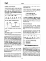
Timer/Counters
An 8254 programmable interval timer provides three 16-bit, 8-MHz timer/countersfor timing and counting
functions such as frequency measurement,event counting, and interrupts. All three timer/counters are cascadedat
the factory. Figure 4-2 shows the timer/counter circuitry.
I 8254
TIMER/
COUNTER
0
|
I
I
CLK
t
I
I
P4
5200
I/O CONNECTOR
P2
I
I
I
oscf }']
EcoS o-r
I
I
I
p r r {s g j E X T C L K O
sMHz
VtFdil
EXT GATE O
GATE
T/C OUT O
OUT
TIMER/
COUNTER
I
l
CLK
GATE
OUT
TIMER/
COUNTER
2
CLK
EXT CLK 1
PIN 43
Filq
EXT GATE 1
T/C OUT 1
I
I
lor
I
3-91
GATE
p t N 4 s d EXT CLK 2
rlrlAr(+5
V
I
XT GATE 2
tc our 2
OUT
L:J
lntervalTimerCircuitBlockDiagram
Fig. 4-2- 8254Programmable
Each timer/counter has two inputs, CLK in and GATE in, and one output, timer/counter OUT. They can be
programmed as binary or BCD down countersby writing the appropriatedata to the command word, as describedin
the VO map section at the beginning of this chapter.
One of two clock sources,the on-board 8-MHz crystal or an external clock can be selectedas the clock input to
each timer/counter. In addition, the timer/counterscan be cascadedby connecting TCO's output to TC1's clock input
and TCl's output to TC2's clock input. The diagram shows how theseclock sourcesare connectedto the timer/
counters.
An external gate source can be connectedto each timer/counter through the I/O connector.When a gate is
disconnected,an on-board pull-up resistor automatically pulls the gate high, enabling the timer/counter.
The output from each timer/counter is available at the VO connector,where it can be used for interrupt generation or for counting functions.
The timer/counters can be programmed to operatein one of six modes, dependingon your application. The
following paragraphsbriefly describeeachmode.
Mode 0, Event Counter (Interrupt on Terminal Count). This mode is typically used for event counting.
While the timer/counter counts down, the output is low, and when the count is complete, it goes high. The output
stays high until a new Mode 0 control word is written to the timer/counter.
Mode 1, llardware-Retriggerable One-Shot. The output is initially high and goes low on the clock pulse
following a trigger to begin the one-shotpulse. The output remains low until the count reaches0, and then goes high
and remains high until the clock pulse after the next trigger.
4-t6
Mode 2, Rate Generator. This mode functions like a divide-by-N counter and is typically used to generatea
real-time clock intemrpt. The output is initially high, and when the count decrementsto 1, the output goes low for
one clock pulse. The output then goeshigh again, the timer/counter reloads the initial count, and the processis
repeated.This sequencecontinues indefinitely.
Mode 3, Square Wave Mode. Similar to Mode 2 exceptfor the duty cycle output, this mode is typically used
for baud rate generation.The output is initially high, and when the count decrementsto one-half its initial count, the
output goes low for the remainder of the count. The timer/counter reloads and the output goes high again. This
processrepeatsindefinitely.
Mode 4, Software-Triggered Strobe. The output is initially high. When the initial count expires, the output
goes low for one clock pulse and then goes high again. Counting is "triggered" by writing the initial count.
Mode 5, Hardware Triggered Strobe (Retriggerable). The output is initially high. Counting is triggered by
the rising edge of the gate input. When the initial count has expired, the output goes low for one clock pulse and
then goes high again.
Digital VO
The 20 available 8255 PPl-baseddigital VO lines can be used to transfer data between the computer and
external devices. The digital input lines of Ports A and C can have pull-up or pull-down resistorsinstalled, as
describedin Chapter 1.
4-t7
ExampleProgramsand Flow Diagrams
Included with the DM5200 is a set of example programs that demonstratethe use of many of the module's
features.These examples are in written in C, Pascal, and BASIC. Also included is an easy-to-usemenu-driven
diagnosticsprogram, 5200DIAG, which is especially helpful when you are first checking out your module after
installation and when calibrating the module (Chapter 5).
Before using the software included with your module, make a backup copy of the disk. You may make as many
backups as you need.
C and Pascal Programs
These programs are source code files so that you can easily develop your own custom software for the
DM5200. In the C directory, DM5200.H and DM5200.INC contain all the functions neededto implement the main
C programs. H defines the addressesand INC contains the routines called by the main programs. In the Pascal
directory, DM5200.PNC contains all of the proceduresneededto implement the main Pascalprograms.
Analog-to-Digital:
SOFTTRIG
Demonstrateshow to use a software trigger for acquiring data.
Timer/Counters:
TIMER
A short progam demonstrating how to program the 8254 for use as a timer.
DigitalVO:
DIGITAL
Simple program that shows how to read and write the digital VO lines.
Interrupts:
INTRPTS
INTSTR
Shows the bare essentialsrequired for using interrupts.
A complete program showing intemrpt-basedstreamingto disk.
BASIC Programs
These programs are sourcecode files so that you can easily develop your own custom software for the
DM5200.
Analog-to-Digital:
SINGLE
SCAN
Demonstrateshow to perform single conversions.
Demonstrateshow to changechannelswhile acquiring data.
Timer/Counters:
TIMER
A short program demonstratinghow to program the 8254 for use as a timer.
Digital VO:
DIGITAL
Simple program that shows how to read and write the digital VO lines.
4-18
Flow Diagrams
The following paragraphsprovide a description and flow diagramsfor performing A./D conversionsand
channel scanning.These diagrams will help you to build your own custom applicationsprograms.
. Single Convert Flow Diagram (Figure 4-3)
This flow diagram shows you the stepsfor taking a single sample on a selectedchannel. A sample is taken each
time you send the Start Convert command. All of the sampleswill be taken on the samechannel and until you
changethe channel by writing a new value to the bottom four bits in the PPI Port B register (BA + 1). Changing this
value before each Start Convert command is issuedlets vou take the next reading from a different channel.
Program8255PPI:PortB out
ChangeChannel?
StartConversion:
BA+8for12-bit;
BA+9for8-bit
End-of-Convert
ReadLSB:
BA+9
(Containsbits 0-3 of 12-bit
conversion)
Read MSB:
BA+8
(Containsbits4-11 of 12-bit
conversion;bits 0-7 of 8-bit
conversion)
Fig.4-3- SingleConversion
FlowDiagram
4-19
. Channel Scanning Flow Diagram (Figure 4-4)
This flow diagram shows you the stepsfor taking a single sample on a sequenceof channels.After programming Port B as a Mode 0 output port, you selectthe starting channel in your sequenceof channelsto be scanned.
After making your initial channel selection,you must allow for enough of a delay in your program for the selected
channel to settle before starting the first A,/D conversion.As soon as the first conversion is started,you can then
immediately select your next channel in the sequence.Once the conversion is started,the signal on the sampled
channel has been "locked in", and you do not have to wait for an end-of-convert transition before programming the
next channel. Selecting the next channel as soon as the conversionofthe previous channel is startedensuresthat
enough time is allowed for the new channel to settle before the next conversion is started,regardlessof your PC
type. Except for the initial delay betweenthe starting channel selectionand first conversion, you do not have to be
concernedwith building delays into your program and the accuracyof the conversionswhen following this program
structure.Note that the data you read in the Read LSB, Read MSB stepswill always be the data from the previously
selectedchannel. not the data from the channel selectedin the SelectNext Channel block.
Program8255 PPI:PortB out
StartConversion:
BA+8for12-bit;
BA+9for8-bit
End-of-Convert
ReadLSB:
BA+9
(Containsbits0-3 of 12-bit
conversion)
ReadMSB:
BA+8
(Contains
bits4-11of 12-bit
conversion:bits0-7 of 8-bit
conversion)
FlowDiagram
Fig.4-4- ChannelScanning
4-20
CHAPTER 5
CALIBRATION
This chaptertells you how to calibrate the DM5200 using the
5200DIAG calibration program included in the example software
packageand the three trimpots on the module. Thesetrimpots
calibratethe A/D convertergain and offset.
This chapter tells you how to calibrate the A,/D converter gain and offset. The offset and full-scale performance
of the module's A/D converter is factory-calibrated.Any time you suspectinaccuratereadings,you can check the
accuracy of your conversionsusing the procedure below, and make adjusts as necessary.Using the 5200DIAG
diagnostics program is a convenient way to monitor conversionswhile you calibrate the module
Calibration is done with the module installed in your system.You can accessthe trimpots at the edge of the
module. Power up the system and let the board circuitry stabilize for 15 minutes before you start calibrating.
Required Equipment
The following equipment is required for calibration:
. PrecisionVoltage Source:-10 to +10 volts
. Digital Voltmeter: 5-ll2 digits
. Small Screwdriver (for trimpot adjustment)
While not required, the 5200DIAG diagnosticsprogram (included with example software) is helpful when
performing calibrations. Figure 5-1 shows the module layout with the three trimpots used for calibration (TRl, TR2,
and TR4) located along the top right edge.
oooo
oootroo
OO rOO
OOB2csrOO
oooooo
oooo
Fig.5-1 -
ModuleLayout
5-3
A/D Calibration
Two proceduresare used to calibrate the A/D converter for all input voltage ranges.The first procedure calibrates the converter for the unipolar range (0 to +10 volts), and the secondprocedurecalibratesthe bipolar ranges
(+5, +10 volts). Table 5-1 shows the ideal input voltage for each bit weight for all three input ranges.
Unipolar Calibration
Two adjustmentsare made to calibrate the A/D converter for the unipolar range of 0 to +10 volts. One is the
offset adjustment, and the other is the full scale,or gain, adjustment.Trimpot TR4 is used to make the offset
adjustment, and trimpot TRl is used for gain adjustment.This calibration procedureis performed with the module
set up for a 0 to +10 volt input range. Before making theseadjustments,make sure that the jumpers on P5 and P6 are
set for this range.
Use analog input channel I (gain = 1) while calibrating the module. Connect your precision voltage sourceto
channel 1. Set the voltage source to +1.22070 millivolts, start a conversion, and read the resulting data. Adjust
trimpot TR4 until it flickers between the values listed in the table at the top of the next page. Next, set the voltage to
+9.49829 volts, and repeat the procedure,this time adjusting TRl until the data flickers between the values in the
table.
Table5-1- A/D ConverterBit Weightsfor All lnput Ranges
ldealInputVoltage(millivolts)
A/D Bit Weight
-5 to +5 Volts
-10to +10Volts
0 to +10Volts
4095 (full-scale)
+4997.6
+9995.'l
+9997.6
2048
0000.0
0000.0
+5000.0
1024
-2500.0
-5000.0
+2500.0
512
-3750.0
-7500.0
+1250.0
256
-4375.0
-8750.0
+625.00
128
-4687.5
-9375.0
+312.5O
64
-4843.8
-9687.5
+156.250
32
-492't.9
-9843.8
+78.125
16
-4960.9
-9921.9
+39.063
8
-4980.5
-9960.9
+19.5313
4
-4990.2
-9980.5
+9.7656
2
-4995.1
-9990.2
+4.8828
1
-4997.6
-9995.1
+2.4414
0
-5000.0
-10000.0
+0.0000
5-4
DataValuesfor CalibratingUnipolarRange(0 to +10volts)
Offset(TR4)
GonverterGain(TRl)
V
InputVoltage= +1.22070
mV InputVoltage= +9.99634
A/D ConvertedData
0000 0000 0000
0000 0000 0001
1 1 1 1 11 1 1 11 0
1 1 1 11 1 1 1 1 1 1 1
Bipolar Calibration
Two adjustmentsare made to calibrate the A/D converter for the bipolar rangesof +5 and +10 volts. One is the
offset adjustment,and the other is the full scale,or gain, adjustment.Trimpot TR2 is used to make the offset
adjustment, and trimpot TR1 is used for gain adjustment.These adjustmentsare made with the module set for a
range of -5 to +5 volts. Before making these adjustments,make sure that the jumpers on P5 and P6 are set for this
range.
Use analog input channel 1 (gain = 1) while calibrating the module. Connect your precision voltage source to
channel 1. Set the voltage source to -4.99878 volts, start a conversion, and read the resulting data. Adjust trimpot
TR2 until it flickers between the values listed in the table below. Next, set the voltage to +4.99634 volts, and repeat
the procedure,this time adjusting TRl until the data flickers betweenthe values in the table.
DataValuesfor GalibratingBipolarRanges(Using-5 to +5 volts)
ConverterGain(TRl)
Offset (TR2)
Inputvoltage= -4.99878V InputVoltage= +4.99634V
A/D ConvertedData
0000 0000 0000
0000 0000 0001
5-5
1 1 1 11 1 1 1 1 1 1 0
1 1 1 1 ' t 1 1 11 1 1 1
APPENDIX A
DM52OOSPECIFICATIONS
DM5200 Characteristics typical@25'c
lnterface
baseaddress,l/O mapped
Switch-selectable
interrupts
Jumper-selectable
Analog Input
inputs
16single-ended
eachchannel........
lnputimpedance,
Inputranges
protection
Overvoltage
time.............
Settling
megohms
.............>10
+10,0 to +10volts
.................+5,
..+35Vdc
1 psec,max
A/D Converter
Type............
Resolution....
Linearity
Conversion
speed..........
time
acquisition
Sample-and-hold
Maximum
throughput
approximation
...........
Successive
......12bits(2.44mY @ 10V;4.88mV @ 20V)
LSB,typ
...................+1
psec,typ
..............20
..5 psec,typ
......40kHz
cMos82cs5
DigitalUO
(Optional NMOS 8255)
& 4 on board)
20 (16at l/Oconnector
4.2V,min
..................0.45V,
max
..2.2V,min;5.5V,max
.-0.3V,min;0.8V,max
100pA, max
mA,max
................1.7
1.0mA,min;-5.0mA,max
Numberof 1ines.........
High-level
outputvo|tage..................
voltage
..................
Low-level
output
High-level
inputvoltage
inputvoltage
Low-level
High-level
outputcurrent,lsource
1sink..........
Low-level
outputcurrent,
Darlington
drivecurrent,I(DAR)
road
Inpur
currenr
. 9:::l::::::::.T:.::::.::::::iiiIrtl
Inputcapacitance,
C(lN)@
F=1MH2.............
outputcapacitance,
C(OUT)<@F=1MHz
Timer/Counter.............
""""" 10pF
.......20
PF
82C54
...........CMOS
(Optional NMOS 8254)
binaryor BCDcounting
Three'16-bit
downcounters;
Programmableoperatingmodes(6)..........................Interruptonterminal
rategenerator;
one-shot;
count;programmable
strobe;
squarewaverategenerator;software-triggered
hardware-triggered
strobe
...........
External
clock(8 MHz,max)or
Counterinputsource
on-board8-MHzclock
...............
externally;
Available
outputs
Counter
usedas PC interrupts
or
to adjacentcounter
cascaded
gateor alwaysenabled
........External
Countergatesource..
Miscellaneous lnputs/Outputs (PC bus-sourced)
+5 volts,+12volts,ground
Current Requirements
240 mA @ +5 volts(1.2W)
Connector
50-pinrightangleheader
A-3
Environmental
to +70'C
..................0
temperature
Operating
to +85"C
...................-40
temperature
Storage
...........0
to 90%non-condensing
Humidity.......
Size
x 0.6"H(90mmx 96mmx 16mm)
3.55"Lx 3.775"W
APPENDIX B
P2 CONNECTORPIN ASSIGNMENTS
B-1
AINl
AIN9
AIN2
AINlO
AIN3
AIN11
AIN4
AIN12
AIN5
AINl3
AIN6
AINl4
AINT
AIN15
AINS
AIN16
P I N2
ANALOG GND
ANALOG GND
EXT GATE O
ANALOG GND
ANALOG GND
ANALOG GND
PA7
PC7
PA6
PC6
PA5
PC5
PA4
PC4
PA3
PC3
PA2
PC2
PA1
PCl
PAO
PC0
PIN 50
EXT CLK O
T/C OUT O
EXT GATE 1
.I
EXT CLK
T/C OUT 1
TIC OUT 2
EXT CLK 2
EXT GATE 2
+12 VOLTS
+5 VOLTS
-12 VOLTS
D I G I T A LG N D
o nF{t
tood
"'
P2 MatingConnectorPart Numbers
PartNumber
Manufacturer
AMP
1-746094-0
3M
3425-7650
B-3
APPENDIX C
COMPONENT DATA SHEETS
IntervalTimer
Intel82C54Programmable
DataSheetReprint
intel'
82C54
CHMOSPROGRAMMABLE
INTERVAL
TIMER
Compatlblewlth all Intel and most
other mlcroprocessorg
Hlgh Speed,"Zero Walt State"
Operatlonwlth I MHz8086/88and
80186/188
HandlesInputsfrom DGto 8 MHz
- 10 MHzfor 82C54-2
Avallableln EXPRESS
- StandardTemperatureRange
- ExtendedTemperatureRange
I
I
I
T
T
I
Three Independent16-bltcounters
Low Power CHMOS
- ICC: 10 mA @8 MHzCount
frequency
completely TTL compailble
Six ProgrammableCounterModes
Blnaryor BCDcounting
Status Read Back Command
AvallableIn 24-PlnDIPand 28-PlnPLCC
I
Thefntel82C54is a high-performance,
CHMOSversionof the industrystandard
8254counter/timer
whichis
designedto solvethe timingcontrolproblemscommonin microcomputer
systemdesign.lt providesthree
independent
16-bilcounters,€achcapableof handlingclockinputsup to 10 MHz.All modesare sottware
programmable.
The 82C54is pincompatible
withthe HMOS8254,andis a supersetof the 8253.
Six programmable
timermodesallowthe 82C54to be usedas an eventcounter,elapsedtime indicator,
programmable
one-shot,
and in manyotherapplications.
The82C54is fabricated
on lntel'sadvanced
CHMOSlll technology
whichprovideslowpowerconsumption
withperformance
equalto or greaterthantheequivalent
HMOSproduct.
The82C54is availabte
in 24-pinDIP
and 28-pinplasticleadedchipcarrier(PLCC)packages.
5
6
I
9
t0
It
231244-3
PLASTICLEADEDCHIPCARRIEF
Dr
0r
231244-1
Flgure1.82C54Block Dlagram
03
Dr
O1
Oz
Dt
Do
.clx 0
our 0
oAtE0
GilO
vcc
t
2l
2
3
2a wr
22 E6
I
21
e5
za
Ar
a
t0
Ao
f
It
cLr 2
OUT2
rt
cLr 1
OATEt
OUTr
t
e
'r0
,|,
rc
t'l
ta
12
r3
2
231244-2
Diagramsarefor pin relerenceonly.
Packagesizesar€not to scate.
Flgure2.82C54Pinout
S€plember 1989
Order Numben 2312{4405
intef
82C54
Table1.PlnDescrlption
Symbol
PinNumber
Dz-Do
DIP
1-8
PLCC
2-9
CLK O
I
OUTO
GATEO
10
10
12
TYPe
Function
t/o
tri-statedata bus lines,
Data:Bidirectional
connectedto systemdatabus.
Clock0: Glockinputof Counter0.
o
0.
Output0: Outputof Counter
0.
Gate0: Gateinoutof Counter
GND
11
12
OUT1
13
GATE1
CLK 1
14
15
16
17
18
20-19
20
o
21
23-22
I
I
Address:Usedto select one of the three Counters
or the ControlWord Registerfor read or write
operations.Normallyconnectedto the system
addressbus.
A1
As
Selects
0
0
Counter0
1
Counter1
0
1
0
Counter
2
1
ControlWord
1
Reoister
cs-
21
24
I
ChipSelectA lowon thisinputenablesthe82C54
to respondto RD andWFIsignals.RD andWFiare
ionoredotheruise.
RD-
22
26
I
WR
23
27
I
Vec
24
ReadGontrol:This inputis low duringGPUread
operations.
WriteControl:This inputis low duringCPUwrite
operations.
Power:+ 5V powersupplyconneetion.
No Connect
GATE2
OUT2
CLK2
Ar,Ao
NC
13
14
16
17
18
19
I
Ground:Powersuoplvconnection,
o
I
Out1:Outputof Counter1
1.
Gate1:Gateinoutof Counter
I
Clock1: Clockinputof Counter1.
I
Gate2: Gateinputof Counter2.
2.
Out2: Outputof Counter
2.
Clock2: Clockinputof Counter
28
'11
, 1 , 1 5 ,2 5
sired delay.Atter the desireddelay,the 82C54 will
interruptthe CPU.Softwareoverheadis minimaland
variablelengthdelayscan easilybe accommodated.
FUNCTIONAL
DESCRIPTION
General
The 82C54is a programmableintervaltimer/counter
designedfor use with lntel microcomputersystems.
It is a generalpurpose,multi-timing
elementthat can
be treated as an array of l/O ports in the system
software.
The 82C54 solves one of the most common problems in any microcomputersystem,the generation
of accuratetime delays under softwarecontrol. Instead of setting up timing loops in software,the programmerconfiguresthe 82C54to matchhis requirements and programsone of the countersfor the de-
Some of the other counter/timerfunctionscommon
to microcomputerswhich can be implementedwith
the 82C54 are:
r
.
o
.
o
o
o
o
3-84
Real time clock
Even counter
Digitalone-shot
Programmablerate generator
Squarewave generator
Binaryrate multiplier
Gomplexwaveformgenerator
Complexmotor controller
intef
82C54
BlockDlagram
CONTROLWORD REGISTER
DATABUSBUFFER
8-bitbutferis usedto inThis3-state,bi-directional,
terfacethe 82C54to the systembus(seeFigure3).
The ControlWordRegister(seeFigure4) is selected
by the Read/WriteLogicwhen Ar, Ao : 11. lf the
CPU then does a write operationto the 82C54,the
data is stored in the ControlWord Registerand is
interpretedas a Control Word used to define the
operationof the Counters.
The ControlWord Registercan only be written to;
status informationis availablewith the Read-Back
Command.
231244-4
Flgure3. BlockDlagramShowlngDataBus
Bufferand Read/WrlteLoglcFunctlons
231244-5
LOGIC
READ/WRITE
The Read/WriteLogicacceptsinputsfromthe syscontrolsignalsfor the other
tem busandgenerates
functionalblocksof the 82C54,A1 and As select
oneof the threecountersor theControlWordReglsinto.A "low" on the RD
ter to be readfrom/written
inputtellsthe 82C54thatthe CPIJ1_S
readingoneof
the counters.A "low" on the WR inputtells the
82C54that the CPUis vy!!!ngeilhera ControlWord
or an initialcount.BothRDandWR arequalified
by
F; FD andWFiare ignoredunlessthe 82C54has
beenselectedby holdingCS low.
Figure 4. Block DlagramShowlng ControlWord
Reglster and Counter Functlons
COUNTERO,COUNTER1, COUNTER2
Thesethree functionalblocksare identicalin operation, so only a singleCounterwill be described.The
internalblock diagramof a singlecounteris shown
in Figure5.
The Countersare fully independent.Each Counter
may operatein a differentMode.
The ControlWord Registeris shown in the figure;it
is not part of the Counteritself,but its contentsdeterminehow the Counteroperates.
3-85
irfief
82C54
storedin the CR and latertranslerredto the CE.The
Control Logic allows one registerat a time to be
loaded from the internal bus. Both bytes are transferredto the CE simultaneously.
CRy and CRl are
cleared when the Counter is programmed.In this
way, if the Counterhas been programmedfor one
byte counts(eithermostsignificantbyte only or least
significantbyte only) the other byte will be zero.
Note that the CE cannotbe writteninto;whenevera
count is written,it is writteninto the CR.
The ControlLogicis also shownin the diagram.CLK
n, GATE n, and OUT n are all connectedto the outside world throughthe ControlLogic.
82C54SYSTEMINTERFACE
231244-6
Flgure5. InternalBlockDiagramof a Counter
The status register, shown in the Figure, when
latched,containsthe currentcontents of the Control
Word Register and status of the output and null
count flag. (See detailedexplanationof the ReadBack command.)
The actualcounterlslabelledCE (for "CountingElement"). lt is a 16-bitpresettablesynchronousdown
counter.
OLy and OL1 are two 8-bit latches.OL stands for
"Output Latch"; the subscriptsM and L stand for
"Most significantbyte" and "Least significantbyte"
respectively.Both are normally referred to as ons
unit and calledjust OL. These latchesnormally"follow" the CE, but if a suitable Gounter Latch Command is sent to the 82C54,the latches"latch" the
presentcount until read by the CPU and then return
to "following"the CE. One latchat a time is enabled
by the counter's Control Logic to drive the internal
bus. This is how the 16-bitCountercommunicates
over the 8-bit internalbus. Note that the CE itself
cannot be read; whenever you read the count, it is
the OL that is beingread.
Similarly,there are two 8-bit registerscalled CRy
and CR1 (for "Gount Register").Both are normally
referredto as one unit and calledjust CR. When a
new count is written to the Counter,the count is
3-86
The 82C54 is treated by the systemssoftwareas an
array of peripherall/O ports; three are countersand
the fourth is a control registerfor MODE programming.
Basically,the selectinputsAo,A1 connectto the Aq,
41 addressbus signalsof the CPU.The G can be
deriveddirectlyfrom the addressbus usinga linear
select method. Or it can be connectedto the output
of a decoder,such as an lntel 8205 for largersystems.
ar t
cl
- cou'|tEi
orD,
LcL
couxrEi
c0 It z2
oul oatE clx
'out
f,6 wt
coutrcR
o^r: clt(' 'out ottr crx'
231244-7
Figure6.82C54SystemInterface
inbf
82C54
OPERATIONAL
DESCRIPTION
Programmingthe 82C54
General
Countersare programmedby writinga ControlWord
and then an initialcount.The controlwordformatis
shown in Figure7.
After power-up,the state of the 82c54 is undefined.
The Mode,count value,and output of all Counters
are undefined.
How each Counteroperatesis determinedwhen it is
programmed.Each Counter must be programmed
beforeit can be used.Unusedcountersneed not be
programmed.
ControlWord Format
A 1 , A e : 1 1e S : O H D : t
D7
All ControlWords are writteninto the ControlWord
Register,whichis selectedwhen 41, Ao : 11.The
ControlWord itself specifieswhich Counteris being
programmed.
By contrast,initialcountsare writteninto the Counters, nol the ControlWord Register.The 41, A9 inputs are used to select the Counter to be written
into.The format of the initialcount is determinedby
the ControlWordused.
WFI:O
D5
sc1 sc0
D5
Da
Ds D2 D1
RW1 RWO M2 M1
SC- SelectGounter:
M-
Ds
MO BCD
MODE:
M2
Ml
scl
sco
0
0
SelectCounter0
0
0
0
Mode0
0
1
SelectCounter1
0
0
1
Mode 1
1
0
SelectCounter2
X
1
0
Mode2
1
1
Read-BackCommand
(SeeReadOperations)
X
1
1
Mode3
1
0
0
Mode4
1
0
1
Mode5
RW - Read/Write:
RW1 RWo
0
0
MO
BCD:
CounterLatchCommand(seeRead
Operations)
0
0
1
Read/Writeleastsignificantbyte only.
1
0
Read/Writemost significantbyteonly.
1
1
Read/Writeleastsignificantbytefirst,
then most significantbyte.
1
BinaryCounter16-bits
BinaryGodedDecimal(BCD)Counter
(4 Decades)
NOTE:Don'tcare bits (X) shouldbe 0 to insure
compatibility
with luture Intelproducts.
Figure7. ControlWordFormat
3-87
intet
82C54
struction sequence is required.Any programming
sequencethat followsthe conventionsabovs is acceptable.
WriteOperations
The programmingprocedurefor the 82C54 is very
flexible.Only two conventionsneed to be remembered:
1) For each Counter,the Control Word must be
written before the initial count is written.
2) The initial count must follow the count format
specifiedin the Control Word (least significant
byte only,most significantbyte only,or leastsignificantbyte and then most significantbyte).
A new initialcount may be written to a Counterat
any time without affecting the Counter's programmedModein any way.Countingwill be atfected
as describedin the Mode definitions.The new count
must follow the programmedcount format.
lf a Counter is programmedto read/write two-byte
counts,the followingprecautionapplies:A program
must not transfer control between writing the first
and secondbyteto anotherroutinewhichalsowrites
into that same Counter.Othenrise,the Counterwill
be loadedwith an inconectcount.
Since the Control Word Register and the three
Countershave separateaddresses(selectedby the
Ar, Ao inputs),and each ControlWordspecifiesthe
Counterit appliesto (SCO,SC1 bits),no specialin-
ControlWordLSBof countMSBof countControlWordLSBof countMSBof countControlWordLSBof countMSBof count-
Counter
0
Counter
0
Counter
0
Counter1
Counter1
Counter1
Counter
2
Counter
2
Counter
2
A1
1
0
0
1
0
0
1
1
1
Ae
1
0
0
1
1
1
1
0
0
ControlWord
Counter
WordControlWord
LSBof countLSBof countLSBof countMSBof countMSBof countMSBof count-
A1
11
11
11
10
01
00
00
01
10
Ae
Counter
0
Counter1
Counter
2
Counter
2
Counter1
Counter
0
Counter0
Counter1
Counter
2
ControlWord
ControlWordControlWord
LSBof countMSBof countLSBof countMSBof countLSBof countMSBof count-
Counter2
Counter1
Counter0
Counter
2
Counter
2
Counter1
Counter1
Counter
0
Counter
0
ControlWordControlWord
LSBof count
ControlWordLSBof countMSBof countLSBof countMSBof countMSBof count-
Counter1
Counter
0
Counter1
Counter
2
Counter0
Counter1
Counter2
Counter0
Counter
2
A1
11
11
't
Ae
1
10
10
01
01
00
00
A1
11
11
01
11
00
01
10
00
10
A6
NOTE:
ln all four examples,all countersare programmedto read/writetwo-bytecounts.
These are only four of many possibleprogrammingsequences.
Figure8. A FewPossibleProgramming
Sequences
ReadOperations
It is often desirable to read the value o{ a Counter
withoutdisturbingthe countin progress.This is easily done in the 82C54.
There are three possiblemethods for readingthe
counters: a simple read operation, the Counter
Latch Command,and the Read-BackCommand.
Each is explainedbelow.The first methodis to perlorm a simple read operation.To read the Counter,
which is selectedwith the A1, A0 inputs,the CLK
input of the selectedCountermust be inhibitedby
usingeitherthe GATE inputor externallogic.Otherwise, the count may be in the processof changing
when it is read,givingan undefinedresult.
3-88
inbf
82C54
grammingoperationsof other Countersmay be insertedbetweenthem.
COUNTERLATCH COMMAND
The secondmethoduses the "CounterLatch Command". Likea ControlWord,this commandis written
to the Control Word Register,which is selected
when A1, Ao : t1. Also like a ControlWord, the
SC0, SC1 bits selectone of the three Counters.but
two other bits, D5 and D4, distinguishthis command
from a ControlWord.
Another feature of the 82C54 is that reads and
writesof the same Countermay be interleaved;lor
example,if the Counteris programmedfor two byte
counts,the followingsequenceis valid.
1. Read least significantbyte.
2. Write new least significantbyte.
3. Read most significantbyte.
4. Write new most significantbyte.
A r , A o : 1 1 ;C S : 0 ; F D : t ; W F : O
D7
D5
D5 Da D3 D2 D1 De
sc1 sc0 0 0 X X X X
lf a Counteris programmedto read/writetwo-byte
counts,the followingprecautionapplies;A program
must not transfercontrol betweenreadingthe first
and secondbyteto anotherroutinewhichalso reads
from that same Counter. Otheruise, an incorrect
count will be read.
SC1,SCO- specifycounterto be latched
scl
sco
Counter
olol
o
0l1l
llol
1
2
1
|
1
READ.BACKCOMMAND
The third method uses the Read-Backcommand.
This commandallows the user to check the count
value, programmedMode, and current state of the
OUT pin and Null Count flag of the setectedcounter(s).
I Read-BackCommand
D5,D4- 00 designatesCounterLatchCommand
X - don't care
The commandis writteninto the ControlWord Register and has the format shown in Figure 10. Thl
commandappliesto the countersselectedby setting their correspondingbits D3,D2,D1: l.
NOTE:
Don'tcarebits (X) shouldbe 0 to insurecompatibility
withfutureIntelproducts.
Figure 9. Counter Latching Command Format
The selectedCounter'soutputlatch (OL)latchesthe
count at the time the Counter Latch Commandis
received.This countis held in the latchuntilit is read
by the CPU (or until the Counteris reprogrammed).
The count is then unlatchedautomaticaliyand the
OL returnsto "following"the countingelement(CE).
This allows reading the contents of the Counters
"on the fly" without affectingcountingin progress.
MultipleCounterLatch Commandsmay be used to
latch more than one Counter.Each latched Counter's OL holdsits countuntilit is read.CounterLatch
Commandsdo not affect the programmedMode of
the Counterin any way.
lf a Counter is latched and then, some time later.
latchedagain before the count is read, the second
CounterLatchCommandis ignored.The count read
will be the count at the time the first CounterLatch
Commandwas issued.
With eithermethod,the count must be read according to the programmedformat; specifically,if the
Counter is programmedfor two byte counts, two
bytesmust be read.The two bytesdo not haveto be
read one right after the other; read or write or pro-
A0,Al:li
GS:O
RD-:1
WF:O
D7
1
D
r ICOUNTISTFTUS
c N T 2 l C N TIlC N T O0
D5:0 : Latch count of selectedcounter(s)
D4: 0 : Latch statusol selectedcounter(s)
D3: 1 : Selectcounter2
D2:1 : Selectcounter1
D1: 1 : Selectcounter0
D9: Reservedfor futureexpansion;must be 0
Figure 10.Read-BackGommandFormat
The read-backcommandmay be usedto latchmultioutput latches (OL) by setting the
&=lgnter
COUNTbit D5:0 and setectingthe desiredcounte(s). This single commandis functionallyequivalent to several counter latch commands,one for
each counterlatched.Each counter'slatchedcount
is held until it is read (or the counter is reprogrammed).That counter is automaticallyunlatched
when read, but other countersremain latched until
they are read.lf multiplecountread-backcommands
are issuedto the same counterwithoutreadingthe
3-89
iffef
82C54
count, all but the first are ignored;i.e., the count
which will be read is the count at the time the first
read-backcommandwas issued.
THISACTION:
A. Writeto the control
wordregister:hl
B. Writeto lhe count
register
fcnlta
C. Newcountis loaderl
inrocE (cR + cE;
The read-backcommandmay also be used to latch
status informationof selectedcounter(s)by setting
ffiruS- bit D4:0. Status must be latched to be
read;statusol a counteris accessedby a read from
that counter.
Da
D
D 71 : O u t P i n i s l
0:OutPinis0
D 61 : N u l cl o u n t
0 : Countavailablefor reading
Ds-Do CounterProgrammed
Mode(SeeFigure7)
Figure 11.Status Byte
NULL COUNTbit DOindicateswhen the last count
writtento the counterregister(CR)has been loaded
into the countingelement(CE).The exact time this
happensdependson the Modeof the counterand is
describedin the ModeDefinitions,
but untilthecount
is loadedinto the countingelement(CE),it can't be
read from the counter.lf the count is latchedor read
before this time, the count value will not reflect the
new count just written.The operationof Null Count
is shownin Figure12.
I
i
I
Nullcount:1
Nullcount:o
Figure12.NullCountOperation
lf multiplestatuslatchoperations
of the counter(s)
areperformed
withoutreadingthe status,all butthe
firstare ignored;i.e.,the statusthat will be readis
the statusof the counterat the timethe firststatus
read-back
command
wasissued.
NULL
OUTPUT
RW1 RWO M 2 M1 MO BCD
COUNT
Command
D7 D5 D5 Da D3 D2 D1 De
Nullcount:1
Itl Qnly the counterspecifiedby the controlword will
have its null count set to 1. Null count bits of oth€r
countersare unaffected.
t2l 1116s counter is programmedtor two-byte counts
(least significantbyte th€n most significantbyte) null
count goes to 1 when the secondbyie is written.
The counterstatusformatis shownin Figure11.Bits
D5 through D0 contain the counter's programmed
Mode exactly as written in the last Mode Control
Word.OUTPUTbit D7 containsthe currentstate of
the OUT pin. This allows the user to monitor the
counter's output via software,possiblyeliminating
some hardwarefrom a system.
D5
CAUSES:
Both countand statusof the selectedcounter(s)
may be latchedsimultaneously
by settingboth
mffi
and SIA-IB bits D5,D4:0. mts ii tunctionallythe sameas issuingtwo separate
read-back
commands
at once,andthe abovediscussions
apply herealso.Specifically,
if multiplecountand/or
statusread-back
commands
areissuedto the same
counter(s)
withoutanyintervening
reads,all butthe
firstareignored.
Thisis illustrated
in Figure13.
lf bothcountandstatusof a counterarelatched,
the
firstreadoperation
of thatcounterwillreturnlatched
status,regardless
of whichwas latchedfirst.The
nextone or two reads(depending
on whetherthe
counteris programmed
for one or two typecounts)
returnlatchedcount.Subsequent
readsreturnunlatchedcount.
DescrlPtion
0
0
0
0
1
0
Readbackcountand statusof
Counter0
.l
0
0
1
0
0
Results
Countandstatuslatched
for Counter
0
{
I
1
I
0
1
1
0
0
Readbackstatusof Counter1
Statuslatchedfor Counter1
Readbackstatusol Counters
2, 1 Statuslatchedfor Counter
1
1
0
1
1
0
0
0
Readbackcountof Counter2
I
0
0
0
1
0
0
Readback countand statusof
Counter1
a
I
0
0
U
1
0
Readback statusof Counter1
1
I
2, but not Counter1
I
1
Countlatchedfor Counter2
Countlatchedfor Counter'1
but not status
Commandignored,status
alreadylatchedfor Counter1
Figure 13.Read.BackCommandExample
3-90
t
intef
82C54
cs
m
0
0
1
0
1
0
0
I
0
0
0
0
0
0
0
1
WR- A r Ao
0
0
0
1
1
0
WriteintoCounter0
WriteintoCounter1
WriteintoCounter
2
WriteControlWord
1
1
1
0
0
0
1
0
1
Readfrom Counter0
Readfrom Counter1
1
1
0
Readfrom Counter2
0
0
0
1
1
1
No-Operation
(3-State)
1
X
X
X
0
1
1
X
X No-Operation(3-State)
X tlo-Operation(S-State)
This allowsthe countingsequenceto be synchronized by_sottware.
Again,OUT does not go high until N
+ 1 CLK pulsesafter the new count of ru is written.
lf an initialcount is writtenwhile GATE : 0, it will
still be loadedon the next CLK pulse.When GATE
goes high,OUT will go high N CLK putseslater;no
CLK pulseis neededto loadthe Counteras this has
alreadybeen done.
Cw r !0
L3!rl
Flgure14.Read/WrlteOperationsSummary
ModeDefinitions
The followingare definedfor use in describingthe
operationof the 82C54.
CLK PULSE:arisingedge,then a fallingedge,in
that order,of a Counter'sCLK lnput.
TRIGGER:arisingedge of a Counter'sGATEinput.
COUNTERLOADING:the transferof a countfrom
the CR to the CE (refer to
the "Functional Description")
l,l - l' | * | I | 3I I I i I s l:FlFEl
Cw. t0
Ll!r3
l,, lxlxlx
l0l0lo
lo
t0
lrr2tzlzlrlolrrl
to
tFFl
MODE 0: INTERRUPTON TERMTNALCOUNT
llode 0 is typicallyusedfor eventcounting.After the
ControlWord is written,OUT is initiallylo-w,and will
remainlow untilthe Counterrsacheszero.OUT then
goes high and remainshigh until a new count or a
new Mode 0 ControlWord is written into the Coun_
ter.
GATE : 1 enablescounting;GATE : 0 disables
counting.GATE has no effect on OUT.
After the ControlWord and initialcount are written to
a Counter,the initialcountwill be loadedon the next
CLK pulse.This CLK pulsedoes not decrementthe
count,so for an initialcount of N, OUT does not go
highuntilN + 1 CLK pulsesafterthe initiatcountis
written.
lf a new count is writtento the Counter,it will be
loadedon the next CLK pulseand countingwillcon_
tinuefrom the new count. lf a two-bytecount is writ_
ten, the followinghappens:
1) Writingthe firstbytedisablescounting.OUTis set
low immediately
(no clockpulserequired).
2) Writingthe second byte allows the new counr to
be loadedon the next CLK pulse.
3-91
l- l- i" l- l3 lt I I I I lt 13lFrl
231244-8
NOTE:
The FollowingConventionsApply To All Mode Timing
Diagrams:
1. Countersare programmedfor binary (not BCD)
countingand for Reading/Writing
leastsignificantbyte
(LSB)only.
2. The counteris alwaysselected(eS alwayslow).
3. CW standsfor "ControlWord',;CW : iO meansa
controlword ol 10, hex is writtento the counter.
4. LSB standsfor "LeastSignificantByte,'of count.
5. Numbersbelowdiagramsare countvalues.
The lowernumberis the leastsignificantbyte.
The upper numberis the most significanibyte. Since
the counteris programmedto Read/WriteLSB ontv,
the most significantbytecannotbe read.
N standsfor an undefinedcount.
Verticallinesshowtransitionsbetweencountvalues.
Figure15.Mode0
inbf
82C54
IIIODE1: HARDWARERETRIGGEBABLE
ONE.SHOT
OUTwill be initiallyhigh.OUT will go low on the CLK
pulsefollowinga triggerto beginthe one-shotpulse,
and will remainlow until the Counterreacheszero'
OUT will then go high and remainhigh untilthe CLK
pulse after the next trigger.
After writingthe GontrolWord and initialcount, the
Counter is armed. A trigger results in loading the
Counterand settingOUT low on the next CLK pulse,
thus startingthe one-shotpulse.An initialcountof N
will resultin a one-shotpulse N CLK cyclesin duration. The one-shotis retriggerable,hence OUT will
remainlow for N CLK pulsesafter any trigger.The
one-shotpulsecan be repeatedwithoutrewritingthe
samecountinto the counter.GATEhas no effecton
OUT.
lf a new countis writtento the Counterduringa oneshot pulse,the currentone-shotis not affectedunless the Counter is retriggered.In that case, the
Counteris loadedwith the new count and the oneshot pulsecontinuesuntilthe new count expires.
MODE2: RATE GENERATOR
This Mode functionslike a divide-by-Ncounter.lt is
typiciallyused to generatea Real Time Clock interrupt.OUTwill initiallybe high.Whenthe initialcount
has decrementedto 1, OUT goes low for one CLK
pulse. OUT then goes high again,the Counterre'
loads the initialcount and the processis repeated.
Mode 2 is periodic;the same sequenceis repeated
indefinitely.For an initialcount of N, the sequence
repeatsevery N CLK cYcles.
GATE : 1 enablescounting;GATE : 0 disables
counting.lf GATE goes low duringan outputpulse,
OUT is set high immediately.A triggerreloadsthe
Counterwith the initialcount on the next CLK pulse;
OUT goes low N CLK pulsesafter the trigger.Thus
the GATE input can be used to synchronizethe
Counter.
After writing a Control Word and initial count, the
Counterwill be loadedon the next CLK pulse.OUT
goes low N CLK Pulsesafter the initialcount is written. This allowsthe Counterto be synchronizedby
software also.
WF
rF
cLx
ctx
GATE
o lE
oul
oul
l - l - I r ,I x l r | 3 l : l t | 3 l ; Fl 3 I I I
WT
wl
CLK
CIK
cAtE
G TE
OUT
l-1"1" l-l: lSll l: l: lllS I
OUI
CWrl.
lS8-a
ISB:5
'WI
cLx
FN
GATE
CLX
oul
GATE
lxiNlrl.
r0l0
rr
13
0l0l0
i2 Ir
15
l0l0l
l.t3l
231244-10
oul
|. i. ir r ix i : iI i3i::l:!l: l: I
231244-9
Figure16.Mode 1
NOTE:
A GATEtransitionshouldnot occur one clock priorto
terminalcount.
Figure17.Mode 2
irilef
82C54
Writinga new count while countingdoes not affect
the curent counting sequence.li a trigger is received after writing a new count but before the end
of the currentperiod,the Counterwill be loadedwith
the new count on the next CLK pulse and counting
will continue from the new count. Othenrise, th5
new count will be loaded at the end of the current
countingcycle.In mode 2, a COUNTof 1 is illegal.
OUTwill be highfor (N + 1)/2 countsand towfor
(N -1)/2 counts.
m
ctr
GATC
sl
MODE 3: SQUAREWAVE MODE
Mode 3 is typicallyused for Baud rate qeneration.
Mode3 is similarto Mode2 exceptfor thjduty cycte
of OUT. OUT wilt initiailybe high.When hatf ing ini_
tialcount has expired,OUT goes low for the remain_
der of the count. Mode 3 is periodic;the sequence
above is repeatedindefinitely.An initialcount of N
results in a square wave with a period of N CLK
cycles.
GATE : 1 enablescounting;GATE = 0 disabtes
counting.lf GATEgoes low whileOUT is low,OUT is
set high immediately;no CLK pulse is required.A
triggerreloadsthe Counterwith the initialcount on
the next CLK pulse. Thus the GATE input can be
used to synchronizethe Counter
After writing a Control Word and initial count, the
Counterwill be loadedon the next CLK pulse.This
allows the Counterto be synchronizedby software
also.
Writinga new count while countingdoes not aflect
the current counting sequence.li a trigger is re_
ceivedafter writinga new count but befol6 the end
of the current half-cycleof the square wave, the
Counterwill be loaded with the new count on the
next CLK pulse and countingwill continuefrom the
new count.Othenrise,the new count will be loaded
at the end of the currenthalf-cycle.
Mode 3 is implementedas follows:
Evencounts:OUT is initiallyhigh.The initialcount is
loadedon one CLK pulse and then is decremented
by two on succeedingCLK pulses.When the count
expiresOUT changesvalue and the Counteris re_
loaded with the initialcount. The above processis
repeatedindefinitely.
Odd counts:OUT is initiallyhigh.The initialcount
minusone (an even number)is-loadedon one CLK
pulse and then is decrementedby two on succeeding CLK pulses.One CLK pulseafter the count expires, OUT goes low and the Counteris reloaded
with the initialcount minus one. SucceedingCLK
pulsesdecrementthe count by two. Whenthe count
expires,OUT goes high again and the Counteris
reloadedwith the initialcount minusone. The above
processis repeatedindefinitely.So for odd counts,
3-93
9!
c!r
oltE
oul
PT
clr
oAt:
oul
l.l"l*l*ll
lil :l: ltl:l:l ! l:l il
231244-11
NOTE:
A GATE transitionshould not occur one clock prior to
terminalcount.
Figure 18.Mode 3
MODE 4: SOFTWARETRtccERED STROBE
OUT will be initiailyhigh.When the initiatcounr ex_
pires,OUT will go low for one CLK pulse and then
go highagain.The countingsequenceis ,'triggered,,
by writingthe initialcount.
GATE : 1 enablescounting;GATE = 0 disables
counting.GATE has no effect on OUT.
After writing a Control Word and initial count, the
Counterwill be loadedon the next CLK pulse.This
pLK putsedoes not decrementthe couni, so for an
initial count of N, OUT does not strobe low until
N + 'l CLK pulsesafter the initialcount is written.
lf a new count is writtenduringcounting,it will be
loadedon the nextCLK pulseand countiigwillcon_
tinuefrom the new count.lf a two-bytecorjntis written, the followinghappens:
intef
82C54
1) Writingthe firstbytehasno etfecton counting.
2) writingthe secondbyteallowsthe newcountto
purse.
cLK
onthenext
beroa.-ded
.'retriggered"by
This allows the sequenceto be
software.OUTstrobeslow N+1 CLKpulsesafter
the newcountof N is written.
Afterwritingthe ControlWordand initialcount,the
willnotbe loadeduntiltheCLKpulseaftera
.",o-'I:t
L",:i"ff!:ll5
x;lXi:
Jnil,?h,|1?,iii""Jl"^:'"i"rl,
strobelow until N + 1 cLK pulsesafter a trigger.
A triggerresultsin theCounterbeingloadedwith.the
initialcounton the next CLK pulse.The counting
sequenceis retriggerable.OUT will not strobe low
for N + 1 CLK pulsesafter any trigger.GATE has
no effect on OUT.
WT
cLx
olrE
our
l"l*l"l*
l0l0l
l3l2l
0
I
I
I
0
0
| FF I FF I FF I
lFFlFElF0l
lf a new count is writtenduringcounting,the current
counting sequence will not be affected. lf a trigger
occursafter the new count is writtenbut beforethe
current count expires,the Counter will be loaded
with the new count on the next CLK pulse and
countingwill continuefrom there.
wl
rF
cLx
CLK
--------'l
olTE
oul
our
WT
FF
cLx
clx
OATE
o tE
n- - --
n---------1
GAIE
OUt
our
l-l'.l-l-lllll
o I o I o I o I fr I
l " l " | * l ' , l * l - | : | : l 3 l : l I l Sl : I l
rl2lrl0lFtl
231244-12
Figure19.Mode 4
re
clx
MODE 5: HARDWARETRIGGEREDSTROBE
(RETRIGGERABLE)
Glt€
OUT will initiallybe high. Countingis triggeredby a
risingedge of GATE.When the initialcount has expired,OUT will go low for one CLK pulse and then
go highagain.
oul
lI " l
I
* l| r
l"
|| * || o I| o I| o I o l r r l r r l
3
2
I
|
0
lTFlFEl
o, o I
r
3
a
I
231244-13
Figure20.Mode5
3-94
intef
82C54
Slgnal
Status
ilodes
Low
Or Golng
Low
0
Disables
countino
Rlslng
Programmlng
Enables
counting
1
2
3
4
OperationGommonto All Modes
Hlgh
When a Control Word is written to a Counter, all
ControlLogicis immediatelyreset and OUT goes to
a knowninitialstate;no CLK pulsesare requiredfor
this.
1) Initiates
counting
2) Resets output
att€r nelit
clock
1) Disables
counting
2) Setsoutput
immediately
hish
1) Disables
counting
2) Setsoutput
immediately
hiqh
GATE
lnitiat€s
counting
Enables
counting
lniliates
counting
Enables
counting
Disables
counting
The GATE input is atways sampled on the rising
edgeof CLK.In Modes0,2,9, and 4 the GATEinput
is level sensitive,and the logic level is sampledon
the risingedge of CLK.In Modes,t,2,9, and S the
GATEinputis rising-edgesensitive.ln these Modes,
a rising edge of GATE (trigger)sets an edge-sensitive flip-flopin the Counter.This flip-flopis then sampled on the next risingedge of CLK; the flip-flopis
reset immediatelyatter it is sampled.In this way, a
trigger will be detected no matter when it occurs-a
high logic leveldoes not haveto be maintaineduntil
the next risingedge of CLK. Note that in Modes 2
and 3, the GATE input is both edge- and level-sensitive. In Modes 2 and 3, if a CLK sourceother than
the system clock is used, GATE should be pulsed
immediatelyfollowingWFIof a new count value.
Enables
countinq
5
lnitiates
countino
Flgure21.GatePlnOperationsSummary
COUNTER
itAx
COUNT
MODE
MIN
COUNT
0
1
1
1
0
0
2
2
0
3
2
4
1
0
0
NOTE:
0 is equivalent
to 216tor binarycounting
and 104for
BCDcounting
Figure 22. Mlnimumand Maxlmuminiilal Counts
New counts are loaded and Counters are decrementedon the lalling edge ot CLK.
The largestpossibleinitialcount is 0; this is equivalent to 216 for binary counting and 1Oafor BCD
counting.
The Counterdoes not stop when it reacheszero. In
ModesO,'1,4,and 5 the Counter"wrapsaround',to
the highestcount,either FFFF hex for binarvcounting or 9999 for BCD counting,and continuei counting.Modes2 and 3 are periodic;the Counterreloads
itself with the initial count and continuescounting
from there.
3-95
intef
82C54
ABSOLUTEMAXIMUMRATINGS*
UnderBias... . . . .0'Cto 70'C
Ambient
Temperature
StorageTemperature ..... -65'to *'150'C
. -0,5 to + 8.0V
SupplyVoltage
....+4Vto *7V
OperatingVoitage
.GND- 2Vto + 6.5V
Voltage
onanyInput..
Voltage
onanyOutput. .GND-0.5Vto V66 + 0.5V
. . .1 Watt
PowerDissipation
'Notice: Sfressesabove those listed under "Absolute MaximumRatings"maycausepermanentdam'
age to the device. Thisis a stressrating only and
functionaloperationof the deviceat these or any
otherconditionsabovethoseindicatedin the operationalsectionsof thisspecificationis not implied.Exposure to absolutemaximumrating conditionsfor
ertendedpeiods mayaffect devicereliability.
D.C.CHARACTERISTICS
Temperature)
(TA:0'C to 7O'C,Vgo:$V+ 10"/o,
GND:0U ffn : -40'C to *85"G for Extended
t2.0
lcc
InputLoadCurrent.
OutoutFloatLeakaoeCurrent
V66 SupplyCurrent
20
Unlte
V
V
V
V
V
pA
pA
mA
lccse
V66SupplyCurrant-Standby
10
pA
Symbol
Vrr
Vru
Vor
Vox
Irr
lorr
Parameter
InputLowVoltage
InoutHiohVoltaoe
OutputLowVoltage
OutputHighVoltage
Mln
-0.5
Max
0.8
2.0
Vcn * 0.5
0.4
3.0
Vec - 0.4
+10
VggSupplyCurrent-Standby
150
pA
Crru
ctto
InputCapacitance
pF
Cour
OutputCapacitance
10
20
20
lccsgr
l/O Caoacitance
A.C.CHARACTERISTICS
(Tn : 0'C to 70'C, V66 : 5V t10o/o, GND :0V) (Tn :
pF
pF
Test Condltlons
lor : 2.5 mA
l o H : -2.5 mA
lnr-r: -100 pA
Vrrl: Vnr: to 0V
Vorrr: Vcc to 0.0V
crkFreq: 'rJ$I;jjrTl
CLKFreq: 96
eS: Vss.
BusV66
All Inputs/Data
AllOutputsFloating
CLKFreq : P6
G : Vcc.AllOtherInputs,
l/O Pins: Vcrun,OutputsOpen
f6: 1MHz
pins
Unmeasured
returned
to GND(5)
-40'C to f 85"Cfor ExtendedTemperature)
(NOIE1)
BUSPARAMETERS
READCYCLE
Symbol
Parameter
tRo
AddressStableBeforeffi J
6 StabteBeforeRD-J
AddressHoldTimeAfterRD-T
FiDPulseWidth
DataDelayfromFD J
tRo
tor
Data Delayfrom Address
RD t to Data Floating
tnv
Time
CommandRecovery
tnn
tsR
tnl
tRR
82C54-2
82C54
Mln
Max
45
0
0
't50
5
200
NOTE:
at Vgs : 2.0V,Vol : 0.8V.
1. AC timingsmeasured
3-96
Mln
30
0
0
Max
ns
ns
ns
85
ns
ns
185
ns
65
ns
95
120
220
90
6
165
Unlte
ns
intef
82C54
A.C. CHARACTERISTICS(Continued)
WBITECYCLE
Symbol
tRw
tsw
twR
tvyyy
tow
two
tnv
82C54
Min
Max
0
Parameter
AddressStableBeforeWF t
eS StaoteBeforeWHJ,
AddressHoldTimeAfterWFi1
WRPutseWidth
DataSetupTimeBeforeWFiT
DataHoldTimeAfterWR1
82C54-2
Min
Max
0
0
0
95
95
0
165
0
0
150
120
0
200
CommandRecoveryTime
Units
ns
ns
ns
NS
ns
ns
ns
CLOCK AND GATE
Symbol
tctr
tpwx
tpwt
Tp
ts
tew
tct
tcs
ton
Too
tooe
twc
twc
two
tcr-
82C54
Min
Max
125
DC
60(3)
60(3)
Parameter
ClockPeriod
HighPulseWidth
Low PulseWidth
ClockRiseTime
ClockFaltTime
GateWidthHigh
GateWidthLow
82C54-2
Min
Max
100
DC
30(3)
50(3)
25
25
25
25
GateSetupTimeto CLKt
GateHoldTimeAfterCLKT
OutputDelayfromCLKJ
9$pqt DetayfromGateJ
CLK Delayfor Loading(a)
Gate Delayfor Sampting(a)
OUT Delayfrom ModeWrite
CLK Set Up for CountLatch
50
50.
50
50
50
50(2)
40
50(2)
0
-5
-40
150
120
55
50
260
45
100
100
55
0
-5
40
240
40
-40
Unite
ns
ns
ns
ns
ns
ns
ns
ns
ns
ns
ns
ns
ns
ns
ns
NOTES:
3;llJ^,liii#Jf
i::;:T:',:*l.each
"t Xf:r"f
3' Low-goingglitches
that violatetpwn, tpwl
risins
crock
edse.
A second
rrisser
within
r20ns(70nsrorthea2cs4-z)
cau-seerors requiringcounterreprogramming.
4. Exceptfor Extendedremp., see Extendb?lay
reinp. e.c. characteristicsbetow.
5. Samplednot looo/otested.Ts : 25.C.
6' ll cLK presentat T1',v6
min then count equalslrl.+2cLK pulses,Tyy6max equals
count N+1 cLK pulse.Tyy6min to
IWCmax,countwill be eitherN + 1 or N + 2 CLK putses.
lil S1*:rt-iii"tiriiffLl
is present
whenwriiinsa newcountvatue,
at rv,v6mincounrer
wir notbetrissered,
at Ty76
8' lf cLK presentwhen writinga counter Latchor ReadBack
command,at T6g min cLK will be relected in count value
latched'at TcL max cLK will not be reflectedin the count
valuelatcGo.'writinga counter Latchor ReadBack
command
betweenT61 min and rvvg max will resultin a latchedcountvallue
whi"n'i" t one leastsignificantbit.
EXTENDEDTEMPERATURE
Symbot
:
-40"Cto *85'Cfor
Parameter
twc
CLK Delayfor Loading
twc
Gate Delayfor Sampling
:xtended
Temperature)
82C54-2
82C54
Min
Max
-25
25
-25
25
3-97
Min
-25
Max
25
-25
25
Units
ns
ns
intef
231244-14
231244-15
RECOVERY
231244-16
inbf
CLOCKAND GATE
23124/-17
t last byt€ ol couni being written
A.C.TESTTNG
tNpUT,OUTPUTWAVEFORM
A.C.TESTINGLOADCIRCUIT
INPUT/OUTPUT
''o;
o.l
r..rro,*r.
<
''o
o.a
,f?1flf;;la1t
A.c.Tesiins:
InpurB
aredriv€n
ar2.4vtotarogic
fora logic"0." Timingmeasur€m€nbar€ madeat 2.OVfor a loglc
"1" and 0.8Vtor a logic"0."
I
or",e
| "i8Jf
|
I
|
*c!.
rtort
I
J.
CL - 150pF
Cg includesllg capacitance
231244-15
Intel82C55AProgrammable
PeripheralInterface
DataSheetReprint
intel'
82C55A
INTERFACE
PERIPHERAL
CHMOSPROGRAMMABLE
I GontrolWord Read-BackCapability
I Direct Bit Set/ResetCaPabilitY
. 2.5 mA DC DriveCapabilityon all l/O
Port OutPuts
I Availablein 40-PinDIP and 44'Pin PLCC
r Availablein EXPRESS
- StandardTemperatureRange
- ExtendedTemperatureRange
I Compatiblewith all Intel and Most
Other MicroProcessors
r Hlgh Speed,"Zero Wait State"
Operationwith 8 MHz8086/88and
80186/188
l/O Plns
a 24 Programmable
r Low PowerCHMOS
I GompletelyTTL GomPatible
CHMOSversionof the industrystandard82554 generalpurpose
The lntel 82C55Ais a high-performance,
lt provides
programmablel/O devicewhich is designedfor use with all Inteland most other microprocessors.
in
maior
modes
of
operation.
groups
3
12
used
programmed
and
in
2
of
pins
may
be
individually
which
ZlitO
The 82C55Ais pin compatiblewith the NMOS8255A and 8255A-5.
In MODE 0, each group of 12 tlo pins may be programmedin sets of 4 and 8 to be inputsor outputs.In
MODE1, each groupmay be programmedto haveI linesof inputor output.3 of the remaining4 pinsare used
for handshakingand interruptcontrolsignals.MODE2 is a strobedbi-directionalbus configuration.
The 82C55Ais fabricatedon Intel'sadvancedCHMOSlll technologywhich provideslow powerconsumption
with performanceequalto or greaterthan the equivalentNMOS product.The 82C55Ais availablein 40'pin
DIP and 44-pinplasticleadedchip carrier(PLCC)packages.
o - f l n
te I I I f 9 i i;;t:
cs
7
R€SEI
GilO
I
m
DI
A0
t0
?c7
It
{c
PC6
l2
DI
xc
t3
D4
PC5
l1
D5
PCI
t5
D6
PCO
r6
17
o7
rc1
PPFEi9EFFFF
231256-3 1
t.*c?nlatau
-
a
q
'
82C55A
231256-1
Figure1.82C55ABlock Diagram
231256-2
Figure2.82C55APinout
Diagrams are lor pin ret€rence only. Package
sizes are not to scale.
3-124
Septembet1987
Order llumbcc 23125G.O04
82C55A
Table1.PlnDescripilon
Symbol
PAg-o
PlnNumber
Dlp
PLCC
1-4
2-5
m
es
5
6
6
7
GND
7
I
lAr-o
8-9
9-10
Type
Nameand Function
t/o
PORTA, PINS0-3: Lowernibbteof an B-bitdataoutputlatch/
butferandan8-bitdatainputlatch.
Thisinputis towduringCpUreadoperations.
EEADCONTROL:
CHIPSELECT:
A lowon thisinputenabtes
the82CSSA
to
respondto RDandWF signats.F-DandWRareignored
otherwise.
SystemGround
ADDRESS:
Theseinputsignals,
in conjunction
RD-andWFi,
controlthe selectionof oneof thethreeportsor the control
wordregisters.
I
I
A1
A6
RD
WF cs
0
0
0
1
0
0
1
0
0
1
1
I
0
0
0
1
1
0
0
1
InputOperatlon(Read)
PortA-DataBus
PortB'DataBus
PortC-DataBus
- DataBus
ControlWord
QutputOperatlon(Wrtte)
0
DataBus- PortA
1
1
0
0
DataBus- PortB
1
0
1
0
0
DataBus- PortC
1
1
1
0
0
DataBus- Control
DisableFunctlon
X
X
X
X
1
DataBus-3-State
X
X
1
1
0
DataBus-3-State
nibbteof an B-bildataoutputlatch/
l9lT C, PINS4-TzUpper
bufferandan 8-bitdatainputbuffer(notatchfor inpui;.Thisport
canbe dividedintotwo4-bitportsunderthe modecontrol.Each
4'bit portcontainsa 4-bitlatchandit canbe usedfor the control
signaloutputs
andstatussignalinputsin conjunction
withports
A andB.
0
0
0
1
0
PCt-q
10-13 11,13-15
vo
PCo-s
PBo-z
't4-17
t/o
t/o
PORTC, PINS0-3: Lowernibbleof port C.
PORTB, PINS0-7: An g-bitdata outputlatch/bufferand an g.
bit data input buffer.
SYSTEMPOWER:* SV powerSuppty.
DATA BUS:Bi-directional,
tri-statedata bus lines,connectedto
systemdata bus.
RESET:A highon this inputclearsthe controlregisterand all
portsare set to the inputmode.
WRITECONTROL:This inputis towduringCpU write
operations.
Vcc
Dz-o
't8-25
26
16-19
20-22,
24-28
29
27-34
30-33,
35-38
t/o
RESET
35
39
I
vm
36
40
PAt-a
37-40
41-44
NC
1 ,1 2 ,
23,94
t/o
PORTA, PINS4-7: Uppernibbleof an 8-bitdata outputlatch/
bufferand an 8-bitdata inoutlatch.
No Connect
intet
82Cs5A
82C55AFUNCTIONALDESCRIPTION
General
peripheral
interface
The82C55Ais a programmable
for usein Intelmicrocomputer
sysdevicedesigned
tems.lts functionis that of a generalpurposel/O
equipment
to the
to interfaceperipheral
component
configusystembus.The functional
microcomputer
by the system
rationof the 82C55Ais programmed
softwareso that normallyno externallogicis necessaryto interfaceperipheraldevicesor structures.
DataBus Bufler
butferis usedto interThis3-statebidirectionalS-bit
face the 82C55Ato the systemdata bus. Data is
transmitted
or receivedby the butferuponexecution
by the CPU.Control
of inputor outputinstructions
words and statusinformationare also transferred
throughthe databusbuffer.
Read/Wrlteand ControlLoglc
The functionof this blockis to manageall of the
internaland externaltransfersof both Data and
Gontrolor Statuswords.lt acceptsinputsfrom the
andin turn,issues
CPUAddressandControlbusses
commands
to bothof the ControlGroups.
GroupA and GroupB Controls
The functionalconfigurationof each port is programmedby the systemssoftware.ln essence,the
CPU"outputs"a controlwordto the 82C55A.The
suchas "mode",
controlwordcontainsinformation
the func"bit set", "bit rgset",etc.,that initializes
of the 82C55A.
tionalconfiguration
Eachof the Controlblocks(GroupA and GroupB)
Control
fromthe Read/Write
accepts"commands"
Logic,receives"controlwords"from the internal
to its asdatabusand issuesthe propercommands
sociatedports.
ControlGroupA - PortA andPortC upper(C7-C4)
ControlGroupB - PortB andPortC lower(C3-C0)
The controlwordregistercan be bothwrittenand
readas shownin the addressdecodetablein th€
pin descriptions.
Figure6 showsthe controlword
When
formatfor both Readand Writeoperations.
thecontrolwordis read,bit D7willalwaysbe a logic
"1", as thisimplies
controlword
modeinformation.
PorteA, B, and C
three8-bitports(A,B, andC).
The82C55Acontains
in a widevarietyof functional
All can be configured
characteristics
by the systemsoftwarebut eachhas
its own specialfeaturesor "personality"to further
of the 82C55A.
enhancethe powerandflexibility
and one
Port A. One8-bitdataoutputlatch/butfer
8-bit input latch butfer.Both "pull-up"and "pulldown"busholddevicesarepresenton PortA.
Port B. One 8-bit data input/outputlatch/buffer.
Only"pull-up"busholddevicesarepresenton Port
B.
and one
Port C. One8-bitdataoutputlatch/butfer
8-bitdatainputbutfer(no latchfor input).Thisport
can be dividedintotwo 4-bitportsunderthe mode
control.Each4-bitportcontainsa 4-bitlatchand it
canbe usedfor thecontrolsignaloutputsandstatus
withportsA andB. Only
signalinputsin conjunction
"pull-up"busholddevicesare presenton PortC.
for
circuitconfiguration
SeeFigure4 for thebus-hold
PortA, B, andC.
3-126
intef
82C55A
231256-3
Flgure3.82c55ABlockDlagramShowlngDataBusBufferand Read/WrlteControlLogtcFunclons
INTEENAL
DATA
'NOTE:
wR
231256-4
Port pins loadedwith more rhan 20 pF capacitancemay not have their rogiclevel guaranleed
tollowinga hardwareresel.
Figure4. PortA, B, C, Bus-holdConfiguration
3-127
intef
82C55A
DESCRIPTION
82C55AOPERATIONAL
CONYROL ITORD
o,
Mode Selectlon
oa
D!
D.
o3
D2
o!
%
J
There are three basic modes of operationthat can
be selected by the system software:
Mode O - Basicinput/output
Mode 1 - StrobedInput/output
Bus
Mode 2 - Bi-directional
/
cRort r
\
foRl c (LowERl
l. lt{PW
0. OUTTUT
Whenthe resetinputgoes "high" all portswill be set
to the inputmodewith all 24 port linesheld at a logic
"one" lev€l by the internalbus hold devices (see
Figure 4 Note). After the reset is removed the
82C55Acan remainin the input mode with no addirequired.This eliminatesthe need
tionalinitialization
for pullup or pulldowndevices in "all CMOS" designs.Duringthe executionof the systemprogram,
any of the other modesmay be selectedby usinga
single output instruction. This allows a single
82C55A to service a variety of peripheral devices
with a simplesoftwaremaintenanceroutine.
FOFT8
l. lilfw
0 . OUTtttT
moDE3ELECltOll
0. ilODE0
I . il(X)E t
/
cRottA
\
foRT c ltt?Ent
l. lN?uT
0. oUT?UT
The modes for Port A and Port B can be separately
defined,while Port G is dividedinto two portionsas
requiredby the Port A and Port B definitions.All of
the output registers,includingthe status flip-flops,
will be resetwheneverthe mode is changed.Modes
may be combinedso that their functionaldefinition
can be "tailored" to almost any l/O structure.For
instance;GroupB can be programmedin Mode 0 to
monitorsimple switch closingsor displaycomputational results, Group A could be programmedin
Mode 1 to monitora keyboardor tape readeron an
interrupt-driven
basis.
FONTA
l.lilruT
O. OUTPUT
iloo€ sELEcTtor'l
0
O. rrOOE
Ol - *IODE I
lx. ||IOOE2
TIOOC
sCTFLAG
I . ACTIVE
231256-6
Flgure6. ModeDefinltlonFormat
and possiblemodecombinaThe modedefinitions
tionsmayseemconfusingat firstbut aftera cursory
reviewof the completedeviceoperationa simple,
willsurface.Thedesignof the
logicall/O approach
82C55Ahastakenintoaccountthingssuchas etfivs PC
cientPCboardlayout,controlsignaldefinition
flexibility
to support
layoutand completefunctional
devicewithno externallogic.
almostanyperipheral
the maximumuse of the
Such designrepresents
pins.
available
SlngleBlt Set/ResetFeature
Anyof the eightbitsof PortC can be Setor Reset
This featurereusinga singleOUTputinstruction.
in Control-based
ducessoftwarerequirements
applications.
231256-5
Figure5. BasicMode Definitionsand Bus
lnterface
WhenPortC is beingusedas status/controlfor
Port
A or B,thesebitscanbe setor resetby usingtheBit
justas if theyweredataoutput
Set/Resetoperation
ports.
3-128
ifier
InterruptControlFunctions
ooiltnol woiD
q
Da
,I
E-lr
4
D.
X
X,
D3
D2
Dt
Do
IIT sET/iESET
I-8fT
O. nESgT
DOI{T
cant
IIT SELgCT
16lTl?15l.Eliltl
l#
+l0l I Iol r l0l I |0l I llol
+l0l0ll lt lel0ll lt lBrl
-lololohflfiFlfi
FLAC
,IT SET/RE8ET
O. ACTIVE
When the 82C55Ais programmed
to operatein
mode1 or mode2, controlsignalsareprovided
that
canbe usedas interrupt
requestinputsto the CpU.
Theinterrupt
requestsignals,
generated
fromportC,
can be inhibitedor enabledby settingor resetting
the associated
INTEflip-flop,usingthe bit set/reset
functionof portC.
Thisfunctionallowsthe Programmer
to disallowor
allowa specificl/O deviceto interrupt
theCpUwithout affectinganyotherdevicein the interrupt
structure.
INTEflip-flopdefinition:
(BIT-SET)-INTE
is SET-|nterruptenabte
(BlT-RESET)-INTE
is RESET-|nterrupt
disabte
Flgure7. Blt Set/ResetFormat
Note:
All Mask flip-flopsare automatically
reset during
modeselectionanddeviceReset.
3-129
intef
82C554
Definitions:
Mode0 BasicFunctional
o Two 8-bitportsandtwo 4-bitports.
conillode 0 (BaslcInput/Output).Thisfunctional
o Anyportcanbe inputor output.
figurationprovidessimpleinputand outputoperao
tionsfor eachof the threeports.No "handshaking"
Outputsare latchec.
is required,data is simplywrittento or readfrom a
o Inpi,rts
are not latched.
specifiedport.
e 16 differentInput/Output
configurations
arepossiblein thisMode.
OperatlngModes
MODE0 (BASTC
|NPUT)
231256-8
MODE0 (BASTC
OUTPUT)
231256-9
3-130
intef
82C55A
MODE0 Port Deflnltlon
B
A
Da
D3
D1
D6
0
0
0
0
0
0
0
0
0
1
0
0
0
0
1
1
1
1
0
0
0
0
1
1
0
1
1
0
0
1
0
1
1
1
1
1
1
1
1
1
0
1
0
1
0
GROUPA
PORTC
PORTA
(UPPER)
OUTPUT
OUTPUT
OUTPUT
OUTPUT
OUTPUT
OUTPUT
OUTPUT
1
1
0
0
1
0
1
OUTPUT
INPUT
INPUT
0
INPUT
1
1
0
0
0
1
1
0
INPUT
INPUT
INPUT
INPUT
INPUT
1
1
1
GROUP
B
PORTC
PORTB
(LOWERI
OUTPUT
OUTPUT
OUTPUT
INPUT
INPUT
OUTPUT
*
OUTPUT
OUTPUT
OUTPUT
OUTPUT
INPUT
0
1
2
3
4
5
6
7
8
I
INPUT
INPUT
INPUT
OUTPUT
OUTPUT
OUTPUT
OUTPUT
NPUT
NPUT
NPUT
NPUT
10
11
12
13
14
15
INPUT
INPUT
OUTPUT
OUTPUT
OUTPUT
INPUT
INPUT
OUTPUT
OUTPUT
OUTPUT
INPUT
OUTPUT
INPUT
INPUT
INPUT
OUTPUT
INPUT
INPUT
OUTPUT
OUTPUT
OUTPUT
INPUT
OUTPUT
INPUT
INPUT
INPUT
MODE0 Configuratlons
CONTROLWORO'2
Dr
De
D5
D.
O!
02
Dr
Do
I
0
0
0
o
0
I
o
Dl
OO
Dr-Do-
CONTROLWORO '3
DrDo%D.03D?Or
07
05
05
o.
Dr
0
o
0
0
Dr
oll
I
PArP&
rc7-PC.
PCI-PCo
Pg7-P8o
231256-10
3-131
intef
82C55A
(Continued)
IIODE0 Conflguratlons
CON'ROL WORDA
orD6orDrD
o,
D6
D!
I
0
0
O.
I
Or
02
Or
Oo
0
0
o
0
?Ar'P\
PAfP\
FCf.
rcl?ct
Erfto
tcrrco
P8r+80
PBr48o
coNtRot ufoRoa0
o,
Da
05
o.
or
or
or
oo
0
0
I
0
0
0
I
PAl\
PAlPAo
PCr+C.
PCi9C.
ftrfto
Er-to
'3r+A!
PBr+80
coNTROLnOAOtrc
o, or Ds o.
coa{rRot tvono rS
ololllololt
Dr
02
ol
oo
lo
PAr4A!
PA/\
PCTPC.
,cr+c.
Er{o
Er-Eo
P8rf6o
P3r+go
Droo..................._
coNtRor ttoRo at
o,
oo
0
Dl
cot{TRoLwoBo a|l
o.
0
or
or
or
oo
o
9ar-P$
PATJ\
rcrPCr
PCfPC.
Erso
Er{o
Ey'9o
PBrfBo
2 3 12 5 6 - 11
3-132
ilODE 0 Conflgurattone(Continued)
ooar?iotwonDrt2
o,
oa
Ds
O.
Dr
Dt
Ot
cot{tioL woFo a,tl
07 Dr O! D.
Oo
rl0l0lrlrl0l0lo
cor{tRoL WOnotlt
Dr Or Dl Dr
Dr
rl0l0
02
Dr
Do
D,
O.
O,
O.
Dr
D:
I
0
Or
D:
Ol
Oo
o
Dr
Do
ffi
rl0l0ltltl0l0ll
Operatlngllodee
ilODE 1 (Strobed Input/Output).This functional
configuration
providesa meansfor transferringl/O
datato or lrom a specifiedport in conjunctionwith
strobesor "handshaking"
signals.In mode1, portA
and Port B use the lineson port C to generateor
acceptthese"handshaking"
signals.
3-133
Mode1 Basicfunctional
Definitions:
o TwoGroups(GroupA andGroupB).
. Eachgroupcontainsone 8-bitdataportand one
4-bitcontrol/dataport.
.
fhg 8-bitdata port can be eitherinputor output
Bothinputsand outputsare latched.
o The4-bitportis usedfor controlandstatusof the
8-bitdataport.
inbf
82C55A
InputControlSlgnalDellnltlon
SE (Strole Input). A "low" on this inputloads
dataintothe inpullatch.
|ilfiEI
Li_i
IBF(lnputBufferFullF/F)
A "high" on this outputindicatesthatthe datahas
beenloadedintothe inputlatch;in essence,an acknowledgement.
IBFis set by STBingJ beinglow
andis resetby the risingedgeof the RD input.
INTR(lnterruptRequest)
roo€ r lFoRr ll
the
A "high"on thisoutputcanbe usedto interrupt
service.
CPU when an inputdeviceis requesting
INTRis set by the STBis a "one", IBF is a "one"
andINTEis a "one".lt is resetby thefallingedgeof
FE. mis procedureallowsan input deviceto reguest servicefrom the CPUby simplystrobingits
dataintothe port.
INTEA
Controlledby bit set/resetof PCa.
INTEB
Controlled
by bit set/resetof PC2.
Itt.
|lFr
riltq
231256-13
Flgure8. iIODE1 Input
231256-14
Flgure9. MODE1 (StrobedInput)
3-134
intef
82C55A
OutputControlSlgnalDellnlUon
6BF lOutput Buffer FuttF/F). The6BF outputwilt
go "low" to indicatethat the CpU has writtendata
outto the specifiedport.TheOEFfff will be set by
the risingedgeof the WF inputand resetby ffi
Inputbeinglow.
6t^
r'-
I lillE
IA
ffi^
Iffi (Actnowledge Input). A "low" on this input
informsthe 82C55Athatthe datafromportA or port
B hasbeenaccepted.
In essence,a responsefrom
the peripheral
deviceindicating
that it hasreceived
the dataoutputby the CPU.
r{?R^
INTR(lnterruptRequest).A "high"'onthis output
can be usedto interruptthe CPUwhen an output
devicehas accepteddata transmittedbv the CpU.
INTRis set whenFffi is a "one".OEF-isa ,,one"
andINTEis a "one".lt is resetby thefallingedgeof
cf,h
wH.
ES
INTEA
Controlledby bit set/resetof PC6
INTEB
Controlledby bit set/resetof pC2.
rxTt
231256- 15
Flgure10.MODEl Output
231256-16
Flgure11.MODE1 (StrobedOurput)
3-135
82C55A
definedas inputor outpulin Mode1 to supporta widevarietyof strobed
PortA andPortB canbe individually
l/O applications.
tA7-P\
Pc.
rc7
Fca
Pcr
COI{YROL fi)RD
COI{TBOL IYORD
?ca
fcr
El. r
lcr, r
Pg"q
?87+Bo
oBFr
ffi"
FORT A - ISIROSCO OUTPUT'
toRT I - |STROSED tt{PUTI
ioirA-tsTtoBEDtNPuD
POFI 8 - ISTROSEOOUTPUTI
231256-17
Figure12.Comblnatlons
of MODE1
Operating Modes
OutputOperatlons
MODE 2 (Strobed Bidirectional Bus l/O).This
functionalconfigurationprovidesa meansfor communicatingwith a peripheraldeviceor structureon a
single 8-bit bus for both transmittingand receiving
data (bidirectionalbus l/O). "Handshaking"signals
are providedto maintainproperbus flow disciplinein
a similar manner to MODE 1. lnterruptgeneration
and enable/disablefunctionsare also available.
6ff lOutputBuffer Full).The OEFoutputwill go
"low" to indicatethatthe CPUhaswrittendataout
to portA.
MODE2 Basic FunctionalDefinitions:
o Used in GroupA only.
o One 8-bit,bi-directional
bus port (PortA) and a 5bit controlport (PortC).
. Both inputsand outputsare latched.
o The S-bitcontrolport (PortC) is used foi control
and status for the 8-bit, bi-directionalbus port
(PortA).
BldirectionalBus l/O Control SignalDefinition
INTR(lnterruptRequest).A highon thisoutputcan
be usedto interruptthe CPUfor inputor outputoperations.
AGK-(Acknowledge).
A "low" on thisinputenables
the tri-stateoutputbutferof PortA to sendout the
data.Othenrise,
the outputbufferwillbe in the high
impedancestate.
INTE 1 (The INTE Flip-Flop Associated wlth
OBF).Controlledby bit set/resetof PC6.
InputOperatlons
STB-(Strobe Input).A "low" on this inputloads
dataintothe inputlatch.
IBF(lnputEuffer FullF/F).A "high"on thisoutput
indicatesthat data has beenloadedinto the input
latch.
INTE2 (TheINTEFlip-FlopAssociatedwlth IBF).
Controlled
by bit set/resetof PCa.
3-136
intef
82C55A
ooilTRoL wonD
05
D.
Dr
D2
oo_F^
E:o
I - INPUT
0'OWPUT
E-K^
xtnT I
1 . INPUT
0 - OUTPUT
SfB^
tBF^
GROUP
B MOOE
0 - I,ODE 0
1 - lrOD€ |
231256-18
Flgure13.MODEControtWord
231256- 1I
Figure14.MODE2
DATA INOI
cPuTo&tc6ta
dEF
IN'R
[dR
stt
IBF
PERIPXCNAL
BUS
oal^ Fnoll
tttrPfiERAL TrOa2C56A
oaTl Fnot
ttc6S toPEnPttEiar
Figure 1S.MODE2 (Bidirectionat)
NOTE:
Anvsequence
@cursbeforeFD is permissibre.
Ug!9-w-Lgg"ursbeforeAeK,:19 g--a_
(INTR= IBFr MASR.STB. n-D+ 6EF. tviASK
o [ffi r ffi;
3-137
intef
82CssA
MOOE2 AND MOOEO IOUTPUT}
MOOE2 AND MODEO {INPUT}
lc!
tilTR^
lc!
?Ar.?Ao
oo.rTBolrcnD
Dr Ot Dr D. D! D, Ot Oo
tar'?\
rc'
6fF^
?icr
IC-K^
OOT{TROLfi)RD
o,
Pc.
txTR^
oa 05 D.
Dt ot
rq
dr^
rca
Fr^
D! oo
3r5^
rca
tBFA
lcr
Et
llo
-srB^
tlF^
t/o
f9fio
MOOE 2 ANO MOOE I (OUTPUT}
M O D E2 A N D M O D E 1 ( I N P U T I
q
?ca
PA7-P\
tAr-tAo
Fct
6ir^
tct
oFr
.%
ACX-^
Pc.
ac-t^
Fc.
fr;^
Pc.
saa
?cs
t8f^
Pct
t8F^
", ".:,-;'":;",
FTMST'X
tB7.?Bo
PS'Eo
FCr
i-o
WR
".
rcz
8TC
ND
rct
tiF.
WR
Pco
tNTn!
Figure16.MODE% Combinations
intet
82C55A
ModeDeflnltlonSummary
MODEO
MODE 1
MODE2
IN
OUT
IN
OUT
PAo I N
PAr IN
PAz IN
IN
IN
IN
IN
IN
IN
IN
IN
OUT
OUT
OUT
OUT
OUT
OUT
OUT
OUT
IN
IN
IN
IN
IN
IN
IN
IN
OUT
OUT
OUT
OUT
OUT
OUT
OUT
OUT
PAg
PAa
PAs
PAo
PAz
IN
IN
IN
IN
IN
OUT
OUT
OUT
OUT
OUT
OUT
OUT
OUT
PBo
PBr
PBz
PBg
PBr
PBs
PBo
PBz
IN
IN
IN
IN
IN
IN
IN
IN
OUT
OUT
OUT
OUT
OUT
OUT
OUT
OUT
Pco
PCr
PCz
PCe
PCa
PCs
PCo
PCz
IN
IN
IN
IN
IN
IN
IN
IN
OUT
OUT
OUT
OUT
OUT
OUT
OUT
OUT
GROUPA ONLY
<+
<---+
e
<.+
MODEO
OR MODE1
ONLY
INTRs INTRg
lBFs GFB
sIEs Affis
t/o
t/o
t/o
INTRa INTRa
INTR1
SfreA t/o
lBFa
t/o
t/o
SEa
lBFa
IfKA
vo
7\CKA
6-rra
SpecialModeComblnatlonConelderailone
Thereare severalcombinations
of modespossible.
Foranycombination,
someor all of the PortC lines
areusedfor controlor status.Theremaining
bitsare
eitherinputsor outputsas definedby a "Set Mode"
command.
Duringa readof Port C, the state ol all the Port C
lines,exceptthe ACKandSTBlines,will be placed
on the databus.In placeof the Affi andSiE line
states,flagstatuswillappearon the databusin the
PCz,PC4,and PC6 bit positionsas illustratedby
Figure18.
Througha "WritePortC" command,
onlythe PortC
pinsprogrammed
as outputsin a Mode0 groupcan
bewritten.No otherpinscanbe atfectedby a "Write
PortC" command,
norcantheinterrupt
enableflags
be accessed.To write to any Port C outputprogrammedas an outputin a Mode 1 groupor to
O-era
changean interrupt
enableflag,the"Set/ResetPort
C Bit" commandmustbe used.
Witha "Set/ResetPortC Bit" command,
anyPortC
linerygrammedas an output(including
INTR,IBF
andOBF)canbe written,or an interrupt
enableflag
canbe eitherset or reset.PortC linesproqrammed
as inputs,including
Affi andSiB tines,aisociated
with PortC are not atfectedby a "Set/ResetPortC
Bit" command.
Writinqto the corlesponding
PortC
bit positionsof the ffi and fg'fines tnitntn"
"Set/ResetPort C Bit" commandwill atfect the
GroupA andGroupB interrupt
enableflags,as illustratedin Figure18.
CurrentDrlveGapablllty
Anyoutputon PortA, B or C cansinkor source2.5
mA.Thisfeatureallowsthe82C55Ato direcflydrive
Darlingtontype driversand high-vottage
displays
thatrequiresuchsinkor sourcecurrent.
3-139
inbf
82C554
ReadingPort C Status
INPUTCONFIGURATION
D5
Da
D3
D2
D1
D7 D5
in Mode0, PortC transfersdatato or fromthe peripheraldevice.
Whenthe82C55Ais programmed
to
functionin Modes1 or 2, PortC generates
or accepts"hand-shaking"
signalswiththeperipheral
device.Reading
the contentsof PortC allowsthe programmerto test or verifythe "status" of each peripheraldeviceand changethe programflow accordingly.
Thereis no specialinstruction
to readthe statusinformationfrom PortC. A normalreadoperationof
PortC is executed
to performthisfunction.
GROUPA
D7
GROUPB
OUTPUTCONFIGURATIONS
D5 D5 D4 D3
D2
D1
oBFAINTEa t/o t/o
De
INTRI
De
INTEs6EFs INTRg
GROUPA
GROUPB
Figure17a.MODE1 StatusWordFormat
D7
D5
D5
Da
D3
D2
D1
Ds
6EF1 INTEl lBFl INTE2INTRa
GROUPA
GROUPB
(Defin€d
ByMode0 or Mode1 Sel€ction)
Figure 17b.MODE2 Status Word Format
Interruot Enable Flaq
INTEB
INTEA2
INTEA1
Posltlon
AlternatePortC PinSignal(Mode)
(OutputMode1)orSTBs(lnputMode1)
PC2
ACK-s
(lnput
PC4
Mode1 or Mode2)
STB1
(Outout
PC6
Mode1 or Mode2
Affia
Figure18.InterruptEnableFlagsIn Modes1 and 2
3-140
intef
82C55A
ABSOLUTEMAXIMUMRATINGS*
AmbientTemperature
UnderBias.. . .0'Cto + 70'C
StorageTemperature ...- 65'Cto* 150'C
- 0.5to + 8.0V
SupplyVoltage
OperatingVoltrage
.....+ 4vto + 7V
Voltage
onanyInput..
. .GND-2Vto + 6.5V
Voltage
onanyOutput. .GND-0.5Vto Vg6 + 0.5V
PowerDissipation
....1Watt
'Notice: Slressesabove those listed under "Absolute MaximumRatings"may causepermanentdamage to the device. Thisis a stressrating only and
functionaloperationof the device at these or any
otherconditionsabovethoseindicatedin the operationalsectionsof thisspecificationis not implied.Exposure to absolutemaximumrating conditionsfor
extendedperiodsmayaffect devicereliability.
D.C.CHARACTERISTICS
TA:OoCto70'C,VCC: +5V t10%,GND:0V(Tn:
Symbol
Parameter
-40'Cto *85'CforExtendedTemperture)
Max
Unlts
0.8
V
Vcc
V
0.4
V
191: 2.5 mA
V
V
lOx: -2.5 mA
IOH: -100pA
Vlx = V6g to 0V
(Note1)
Vgp: V66 to 0V
(Note2)
TestCondltions
vru
InputLow Voltage
Min
-0.5
Vrx
Vor
Von
InputHighVoltage
2.O
OutputLowVoltage
I11-
lnputLeakage
Cunent
r1
pA
loru
OutputFloatLeakageCurrent
r10
pA
lonn
Darlington
DriveCurrent
r 2.5
(Note4)
mA
PortsA, B,C
Rsn : 500O
Vs1 : 1.7V
lput
Port Hold Low LeakageCurrent
+50
+300
pA
lpxx
Port Hold HighLeakageCurrent
-50
-300
pA
lpHlo
Port Hold Low OverdriveCurrent
-350
p"A
V9g1 : 1.0V
PortA only
V9g1 : 3.0V
PortsA, B, C
V6g1 : 0.8V
lpxno
PortHoldHighOverdrive
Current
+ 350
pA
V9g1 : 3.0V
lcc
V6sSupplyCunent
10
mA
lccse
Vg6 SupplyCunent-Standby
10
pA
(Note3)
V66 : 5.5V
Vtru: VCCor GND
PortConditions
It llP : Open/High
OlP : OpenOnly
WithDataBus:
High/Low
eS: High
Reset: Low
PureInputs:
Low/High
OutputHighVoltage
3.0
Vss - 0.4
NOTES:
1.PinsA1,Ao,G, WF,FiD,Reset.
2, ?au-ALls;fgrts-!.c,-_
3. Outputsopen.
4. Limitoutputcurrentto 4.0 mA.
3-141
intef
82C55A
CAPACITANCE
T4 : 25'C, Vgg :QltlP : 9Y
Parameter
Symbol
Mar
Ctr.t
InputCapacitance
10
Unlts
pF
ctrc
l/O Capacitance
20
pF
Mln
TestGondltlons
plns
Unmeasured
returned
to GND
fc : 1 MHz(s)
NOTE:
5. Samplednot 100%tested.
A.C. CHARACTERISTICS
TA : 0'to 70'C,VCC: +5V 1100/",GND : 0V
TA : -40'C to +85'C for ExtendedTemperature
BUS PARAMETERS
READ CYCLE
Symbol
82C55A-2
Parameter
Mln
tnR
tRR
AddressStableBeforeRD-J
AddressHoldTimeAfterF-DT
tnR
RDPulseWidth
tno
DataDelayfromRD-J
top
RD t to DataFloating
RecoveryTimebetweenFD/WH
tnv
Unlts
llax
0
ns
0
ns
150
ns
10
120
ns
75
ns
Test
Condltlons
ns
200
WRITECYCLE
Symbol
82C55A.2
Unlta
Test
Condltlons
PortsA & B
20
ns
ns
ns
Parameter
Mln
tRw
AddressStableBeforeWF !
0
twR
AddressHoldTimeAfterWRt
20
llax
PortC
tww
WR PulseWidth
100
ns
tow
DataSetupTimeBeforeWFIf
100
ns
two
DataHoldTimeAfterWF I
30
ns
PortsA & B
30
ns
PortC
3-142
82C55A
Symbol
82C55A.2
Parameter
Mln
twa
trn
txn
WR: l toOutput
Peripheral
DataBeforeRD
0
ns
200
ns
STBPulseWidth
100
ns
Per.DataBeforeffi Xign
Per.DataAtterSTBHigh
20
ns
50
ns
tsr
tps
txo
twoe
ns
ns
tRx
teo
350
0
Peripheral
DataAfterFiD
AeR PutseWidth
tpx
Max
Unlts
Condltlons
ACK:0toOutput
Iffi : 1 to OutputFloat
20
175
NS
250
ns
150
ns
ttog
WF i : l to OB F : o
A G K -O
: t o O B F :1
150
ns
tsre
$B:0tolBF:1
150
ns
tnrg
R-D:ltolBF:0
150
ns
lRr
RD:OtoINTR:0
200
ns
tsr
tnrr
twn
tnEs
SiB:lto|NTR:1
150
Affi=lto]NTR:1
150
WR:OtoINTR:0
200
ns
ns
ns
ns
ResetPulseWidth
500
Test
seenote1
seenote2
NOTE:
1. INTRI mayoccuras earlyas WFJ .
2. Pulsewidthol initialResetpulseafterPoweron mustbe at least50 pSec.Subsequent
Resetpulsesmaybe 500 ns
minimum.
3-143
82C55A
WAVEFORMS
moDE0 (BASICINPUT)
231258-22
lroDE 0 (BAsrcoUTPUT)
2 1256-23
3-144
intef
82C55A
WAVEFORMS(continued)
MODE1 (STROBED
|NPUT)
ctT
r3t
txTt
F-D
lt{PuttFofl_
_
PCRIPHCRAI
_
MODEI (STROBED
OUTPUT)
f,R
(5F
IflTR
lcr
ot ttrrr
231256-25
3-145
82C55A
WAVEFORMS(continued)
MODE2 (BTDIRECTTONAL)
OATA FROM
t080 To 82€5
?CNIPHEiAI
il,s
DATA
'CIIPXERAL TO 1266
DATAFROM
T265?O PERIIXERAL
DATA
!255 tO s030
231256-26
Notc:
Any sequencewhereWFi occurs b€foreFfi AND SIB- occursbeforeFD is permissible.
flNTF : IBF o il[4ffi r $tEi o FE + 6EF. ilfiA3k o flffi e ffi;
WRITE TIiIING
READTIMING
231256-28
231256-27
A.C. TESTINGINPUT,OUTPUTWAVEFORM
231256-25
A.C.TestinglnputsAr€ DrivenAt 2.4Y For A Logic1 And 0.45V
Are Made At 2.0V For A
For A Logic 0 TimingMeasurements
Logic1 And 0.8 For A Logic0.
A.C. TESTINGLOAD CIRCUIT
Iq'rloPF
231256-30
'V6y1 ls Set At VariousVoltsgesDuringTostingTo Guarantee
Th€ Spgcitication.
Cg IncludesJig Capacitance.
APPENDIX D
WARRANTY
LIMITED WARRANTY
andproducesto be free
RealTime Devices,Inc. warrantsthehardwareandsoftwareproductsit manufactures
from defectsin materialsandworkmanshipfor oneyearfollowingthedateof shipmentfrom REAL TIME DEVICES.This warrantyis limited to theoriginalpurchaserof productandis not fransferable.
During the oneyearwarrantyperiod,REAL TIME DEVICESwill repairor replace,at its option,anydefective
productsor partsat no additionalcharge,providedthattheproductis returned,shippingprepaid,to REAL TIME
DEVICES.All replacedpartsandproductsbecomethepropertyof REAL TIME DEVICES.Before returning any
product for repair, customersare required to contactthe factory for an RMA number.
THIS LIMITED WARRANTY DOESNOT EXTEND TO ANY PRODUCTSWHICH HAVE BEEN DAMAGED AS A RESULTOF ACCIDENT,MISUSE,ABUSE (suchas:useof incorrectinput voltages,improperor
insufficientventilation,failureto follow theoperatinginstructionsthatareprovidedby REAL TIME DEVICES,
beyondrhecontrolof REAL TIME DEVICES),oR AS A RESULTOF
"actsof God" or othercontingencies
SERVICEOR MODIFICATION BY ANYONE OTHERTHAN REAL TIME DEVICES.EXCEPTAS EXPRESSLYSETFORTHABOVE, NO OTHERWARRANTIESARE EXPRESSEDOR IMPLIED, INCLUDING,
BUT NOT LIMITED TO, ANY IMPLIED WARRANTIES OF MERCHANTABILITY AND FITNESSFOR A
PARTICULARPURPOSE,AND REAL TIME DEVICESEXPRESSLYDISCLAIMS ALL WARRANTIESNOT
STATED HEREIN. ALL IMPLIED WARRANTIES, INCLUDING IMPLIED WARRANTIES FOR
MECHANTABILITY AND FITNESSFORA PARTICULARPURPOSE,ARE LIMITED TO THE DURATION
OF THIS WARRANTY. IN THE EVENT TI{E PRODUCTIS NOT FREEFROM DEFECTSAS WARRANTED
ABOVE, THE PI]RCHASER'SSOLEREMEDY SHALL BE REPAIROR REPLACEMENTAS PROVIDED
ABOVE. UNDER NO CIRCUMSTANCESWILL REAL TIME DEVICESBE LIABLE TO THE PURCHASER
OR ANY USERFOR ANY DAMAGES,INCLUDING ANY INCIDENTAL OR CONSEQI.IENTIALDAMAGES,EXPENSES,LOST PROFITS,LOST SAVINGS,OR OTHERDAMAGES ARISING OUT OF THE USE
OR INABILITY TO USE THE PRODUCT.
SOME STATESDO NOT ALLOW THE EXCLUSIONOR LIMITATION OF INCIDENTAL OR CONSEQUENTIAL DAMAGES FOR CONSUMERPRODUCTS,AND SOMESTATESDO NOT ALLOW LIMITA.
TIONS ON HOW LONG AN IMPLIED WARRANTY LASTS,SOTHE ABOVE LIMMATIONS OR EXCLUSIONSMAY NOT APPLY TO YOU.
THIS WARRANTY GIVES YOU SPECIFICLEGAL RIGHTS,AND YOU MAY ALSO HAVE OTHER
RIGHTSWHICH VARY FROM STATETO STATE.
D-3
DM5200Board User-SelectedSettings
Basel/O Address:
(hex)
(decimal)
IRQSource& ChannelSelected:
Source(P7):
IRQChannel#(P3):