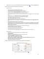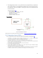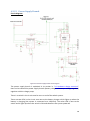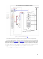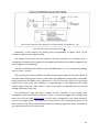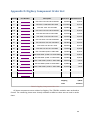
1
UNIVERSIDAD AUTONOMA DE MADRID ESCUELA POLITECNICA SUPERIOR PROYECTO FIN DE CARRERA Development of a ZigBee Wireless Sensor Node Ingeniería de telecomunicación Daniel Blanco Lauzurica Mayo, 2012 Development of a ZigBee Wireless Sensor Node AUTOR: Daniel Blanco Lauzurica TUTOR: Martin Ekström PONENTE: Gustavo D. Sutter Email: [email protected] Division of Intelligent Future Technologies, School of Innovation Design and Engineering Mälardalen University Västerås, Sweden Mayo 2012 Resumen Una red inalámbrica de sensores (WSN, del inglés Wireless Sensor Network) es una red compuesta por sensores autónomos (nodos) cuya finalidad es monitorizar alguna característica del entorno como podrían ser: temperatura, presión, humedad, movimiento, sonido, luminosidad, etc. Los nodos usan un sistema de radiofrecuencia para enviar la información recogida por los sensores a una unidad de procesamiento central (CPU). La comunicación entre un nodo y la CPU puede darse directamente (un único salto) o a través de otros nodos de la red (en varios saltos). Algunas WSN también permiten el control de sus nodos desde la CPU. Cada nodo sensor normalmente consta de los siguientes componentes principales: un microcontrolador, diferentes sensores, un transceptor de radio y una batería u otra fuente de alimentación. También suele haber varios componentes empleados para acondicionar las señales eléctricas y la alimentación a los requisitos de los componentes principales de forma que estos se puedan interconectar; dispositivos como reguladores de tensión, amplificadores, resistencias, condensadores, conversores A/D u osciladores. El objetivo de este proyecto es diseñar y construir un nodo de una red de sensores, así como programar el microcontrolador que integrará de forma que cubra una funcionalidad básica: deberá ser capaz de medir el consumo energético de su propio módulo de radiofrecuencia basado en ZigBee y de enviar los datos de estas mediciones por radio a otros nodos de la red. Este objetivo fue alcanzado: se construyeron y programaron dos nodos idénticos y su funcionalidad se comprobó con resultados satisfactorios. Los PCBs para el sistema han sido diseñados con EagleCAD 5.11. Los nodos WSN se construyeron principalmente con componentes SMT (Surface Mount Technology). El microcontrolador que llevan los nodos es un PIC24 y ha sido programado en C con mikroC Pro 5.4. El microcontrolador recibe las señales de los sensores y las digitaliza, a continuación almacena las muestras y finalmente las envía al módulo de ZigBee desde donde se transmiten por radio. El nodo lleva un Puerto USB que permite su conexión con un PC. Palabras clave: WSN, ZigBee, EagleCAD, mikroC, PIC, red de sensores. I Abstract A Wireless Sensor Network (WSN) is a network made up of small autonomous sensors (nodes). Its purpose is to monitor certain environmental variable such as temperature, pressure, humidity, motion, sound, brightness, etc. These nodes use a radiofrequency system to deliver the information gathered by the sensors to a central processing unit (CPU). The communication between a node and the CPU might happen either directly or step by step through different nodes within the network. Some WSN can also be controlled from the CPU. Each sensor node usually consists of the following main components: a microcontroller, different sensors, a radio transceiver and a battery or another source of power. There are also several components which are used to adequate the electric signals and the power supply to the requirements of the main components; in this category might fall devices such as voltage regulators, amplifiers, resistors, capacitors or oscillator sources. The goal of this thesis is to design and build a WSN node and to program its microcontroller so it covers a basic functionality: it should be able to measure the power consumption of its own ZigBee radio module and to send the collected data to other network nodes. This goal was achieved. Two similar ZigBee nodes were built and programmed, and their functionality was tested. The PCBs for the system were designed in EagleCAD 5.11. The WSN nodes were built using SMT (Surface Mount Technology) devices mainly. A PIC24 microcontroller was mounted on the WSN node and programmed in C with mikroC Pro 5.4. The PIC24 microcontroller receives the signals from the sensors and converts them to digital; then it stores the digitalized data to finally deliver them to its ZigBee radio module where they are sent by radio. A USB connection has been implemented to enable the communication between the WSN node and a PC. Keywords: WSN, ZigBee, EagleCAD, mikroC, PIC. II Preface I would like to thank Martin Ekström for his assistance and guidance during the development of this MSc. Thesis. III Table of Contents Resumen .................................................................................................................................................. I Abstract ................................................................................................................................................... II Preface ................................................................................................................................................... III Table of Figures ...................................................................................................................................... VI List of Tables ......................................................................................................................................... VII 1. 2. Introduction .................................................................................................................................... 1 1.1 Motivation and Objectives ...................................................................................................... 1 1.2 Document Description ............................................................................................................ 2 Methodology and Working Plan ..................................................................................................... 3 2.1 3. 4. Available Means and Tools ..................................................................................................... 3 State of the Art................................................................................................................................ 4 3.1 Wireless Sensor Networks ...................................................................................................... 4 3.2 ZigBee and the IEEE Std 802.15.4 ........................................................................................... 5 Hardware Design........................................................................................................................... 11 4.1 Hardware Design Overview .................................................................................................. 11 4.1.1 The Sensors ................................................................................................................... 12 4.1.2 The Power Supply Branch ............................................................................................. 12 4.1.3 The ZigBee Radio Module ............................................................................................. 12 4.1.4 The Connectors ............................................................................................................. 12 4.2 Components .......................................................................................................................... 13 4.2.1 Microcontroller: PIC24FJ256GB106 .............................................................................. 13 4.2.2 ZigBee Module: ETRX351 .............................................................................................. 16 4.2.3 Battery Charger: MAX 1811 .......................................................................................... 18 4.2.4 Voltage Regulator: XC6203X332 ................................................................................... 19 4.2.5 Charge Pump: MCP1253-33X50 .................................................................................... 20 4.2.6 Current Shunt Monitor: INA196.................................................................................... 21 4.2.7 Temperature Sensor: TMP36 ........................................................................................ 22 4.2.8 Accelerometer: ADXL337 .............................................................................................. 23 4.2.9 Microphone: ADMP441 ................................................................................................ 24 4.2.10 Crystal Oscillator ........................................................................................................... 26 4.2.11 Connectors .................................................................................................................... 26 4.2.12 Power Supply Branch .................................................................................................... 28 IV 4.3 Layout Design ........................................................................................................................ 29 5. Construction.................................................................................................................................. 30 6. Software Development: The PIC24 Firmware............................................................................... 32 6.1 Configuration Words ............................................................................................................. 33 6.1.1 Oscillator Configuration ....................................................................................................... 34 6.2 Pin Configuration .................................................................................................................. 35 6.3 UART Configuration .............................................................................................................. 36 6.4 A/D Converter Initialization .................................................................................................. 38 6.5 USB Module Initialization...................................................................................................... 42 6.6 The Main Loop ...................................................................................................................... 45 7. Result ............................................................................................................................................ 47 8. Discussion...................................................................................................................................... 47 9. Conclusion ..................................................................................................................................... 48 REFERENCES ............................................................................................................................................. 49 GLOSSARY ................................................................................................................................................ 52 Appendix A. Developed Firmware For The PIC24 ................................................................................ 54 UART_module.c ................................................................................................................................ 54 AD_module.c..................................................................................................................................... 55 Headers.h .......................................................................................................................................... 57 USBdsc.c ............................................................................................................................................ 57 Final_program.c ................................................................................................................................ 59 Appendix B. Hardware Design Schematic ............................................................................................. 66 Appendix C. Layout Design ................................................................................................................... 67 Top Layer........................................................................................................................................... 67 Bottom Layer..................................................................................................................................... 68 Appendix D. Digikey Component Order List ......................................................................................... 69 Appendix E. User Manual...................................................................................................................... 70 Appendix F. Traducciones ..................................................................................................................... 72 Appendix G. Presupuesto...................................................................................................................... 77 Appendix H. Pliego de Condiciones ...................................................................................................... 78 V Table of Figures Figure 3.1: WSN monitoring an active volcano [32] ............................................................................... 5 Figure 3.2a: ZigBee Protocol Stack.......................................................................................................... 6 Figure 3.2b: IEEE 802.15.4 Superframe Structure [9] ............................................................................. 8 Figure 3.2c: ZigBee Network Topologies [33] ....................................................................................... 10 Figure 4.1: Hardware Design Block Diagram......................................................................................... 11 Figure 4.2.1: PIC 24 Circuit Diagram [11] .............................................................................................. 15 Figure 4.2.2a: ETRX351 Hardware Description [12].............................................................................. 16 Figure 4.2.2b: UART Interface with Flow Control [14] .......................................................................... 17 Figure 4.2.3: Typical Operating Circuit [15] .......................................................................................... 18 Figure 4.2.4: XC6203E332 Output Voltage vs. Input Voltage [16] ........................................................ 19 Figure 4.2.6a: INA 193-198 Simplified Circuit [18] ................................................................................ 21 Figure 4.2.6b: INA196 Circuit Diagram ................................................................................................. 22 Figure 4.2.7: TMP36 Circuit Diagram .................................................................................................... 23 Figure 4.2.8a: ADXL337 Functional Block Diagram [21]........................................................................ 23 Figure 4.2.8b: ADXL337 Circuit Diagram ............................................................................................... 24 Figure 4.2.9a: ADMP441 Functional Block Diagram [22] ...................................................................... 25 Figure 4.2.9b: ADMP441 Circuit Diagram ............................................................................................. 25 Figure 4.2.10: 12MHz Crystal Circuit Diagram ...................................................................................... 26 Figure 4.2.11a: Stereo Jack Connector Circuit Diagram........................................................................ 26 Figure 4.2.11b: IDC10 Connector Circuit Diagram ................................................................................ 27 Figure 4.2.11c: USB Circuit Diagram ..................................................................................................... 27 Figure 4.2.12: Power Supply Branch Circuit Diagram ........................................................................... 28 Figure 5: The two boards, one showing the top and the other the bottom......................................... 31 Figure 6.1.1a: PIC24FJ256GB110 Family Clock Diagram [11] ............................................................... 34 Figure 6.1.1b: PIC24 96MHz PLL Block Diagram [11] ............................................................................ 35 Figure 6.2: Block Diagram of a Typical Shared Port Structure [11]....................................................... 35 Figure 6.3: Frame Structure for UART Communications [25] ............................................................... 36 Figure 6.4a: A/D Converter Block Diagram [11].................................................................................... 39 Figure 6.4b: A/D Converter Analog Input Model [11]........................................................................... 40 Figure 6.4c: A/D Converter Sample/Convert Sequence [27] ................................................................ 41 Figure 6.4d: A/D Converter Transfer Function [11] .............................................................................. 41 Figure 6.5: USB-HID Terminal ............................................................................................................... 45 Figure 6.6: Program Flowchart ............................................................................................................. 46 Figure B: Hardware Design Schematic .................................................................................................. 66 Figure C1: Layout Design: Top Layer ..................................................................................................... 67 Figure C2: Layout Design: Bottom Layer ............................................................................................... 68 VI List of Tables Table 3.2: IEEE 802.15.4 Frequency Bands and Data Rates [9]............................................................... 7 Table 4.2.4: XC6203X332 Electrical Characteristics [16]....................................................................... 19 Table 6.3a: ETRX351 Firmware R305 Supported Baud Rates [13] ........................................................ 36 Table 6.3b: PIC24 UART Baud Rates for an Instruction Cycle Frequency (FCY) of 16MHz [26] ............ 37 Table 6.3c: EM351 UART Baud Rate Divisors and Errors for Common Baud Rates [14] ...................... 38 Table D: Digikey Component Order List ................................................................................................ 69 VII 1. Introduction This project covers the design and construction (schematics and PCB) of a WSN node, as well as the programming and testing of its microcontroller. The node will use a ZigBee RF module to communicate and it will have an embedded sensor to measure the energy consumption of this very same RF module. The microcontroller will be programmed in C. 1.1 Motivation and Objectives Wireless Sensor Networks are intended for low data rate applications that involve certain kind of sensing and actuation [2]. They might be suitable for applications that have or combine some of the following characteristics: harsh environments (mines, nuclear plants, underwater, industrial plants…), large area or areas with difficult access (forest, fields, mountains, sewer system, buildings…), short sensor range, a large amount of nodes is necessary, little or no maintenance and infrastructure is possible, usually because the environment conditions do not allow them. The node will be a prototype which primary function is to monitor the power consumption of its own RF module. The possible secondary functions will depend on the sensors that the node might integrate. These secondary functions and the potential application of the node will be limited by several factors such as the size and weight of the node, the battery life time, the components and materials used, etc. Finally, although not within the scope of this thesis, the node will be part of a ZigBee network. Hopefully, it will be, then, used to extract different energy models of the RF module when it is working under different environments and conditions. The school of Innovation Design and Technology of Mälardalen University holds two projects, named GAUSS and TESLA, aimed to achieve predictability in time-critical wireless communication which takes place harsh environments. Especially those environments where there is a high degree of electromagnetic interference. The main application area of these two projects is time-critical industrial processes. The outcome of this project, that is, the nodes will hopefully be used in these wider projects. This might be somehow understood as the motivation of this work. The objectives of the project are listed next: Design and construction (schematics and PCB) of a WSN node. Microcontroller programming in C. The microcontroller will be a PIC24; more specifically a PICFJ256GB106 which manufacturer is Microchip Technology. A ZigBee module will be used for the communication. 1 An embedded sensor in the node will measure the energy consumption of the ZigBee module. The data gathered by this sensor will be either stored in the microcontroller memory or sent by radio or wired connection. The ZigBee module and the microcontroller will communicate with each other through a UART interface. It is implemented by the use of a UART (Universal Asynchronous Receiver-Transmitter) on both ends. The board will have a Stereo Jack socket connected to the microcontroller by an I2C bus. A battery charger and a voltage regulator will be used to power all the other components. A USB port will be used to charge the batteries and to power up the system. It will also provide a link for communications with a PC. An accelerometer will be one of the sensors on the board. The board will be tested and its functionality checked. 1.2 Document Description After the introduction, section 2. Methodology and Working Plan, explains the stages that were taken in the project as well as the means and tools that were used. Section 3. State of the Art provides an introduction to Wireless Sensor Networks and ZigBee. This is not really necessary to understand the carrying out of the project, but it is to understand its purpose and perhaps some design decisions. To understand well the carrying out of the project it is recommended to have knowledge of hardware design and some experience programming microcontrollers. Under section 4. Hardware Design, can be found subsection 4.1 Hardware Design Overview, which reading is strongly recommended since it explains how the system works (Figure 4.1 shows a functional diagram of the system). Subsection 4.2 Components shows the features of each individual component and explains its function a bit deeper, there is usually provided a circuit diagram showing the implemented connections. Section 5. Construction explains details and stages of the manufacturing process. Section 6. Software Development: The PIC24 Firmware explains how the PIC24 was programmed: first it explains the part of the program that defines the configuration of its modules (UART, A/D converter, USB, Oscillator), its pins and the Configuration Words (registers that define the PIC24 behaviour); then the rest of the program is explained, just the main loop and the functions that intervene. Sections 7, 8 and 9 present the Results, Discussion and Conclusion, respectively. Finally, in the appendices can be found: the code, the whole hardware design schematic, the layout design, the component order list and a user manual. 2 2. Methodology and Working Plan The project will be carried out on the following sequential stages: 1. Research: it will be done during the whole development of the project and whenever it is necessary. A deeper research will be needed at the beginning of each stage to get acquainted with the topic and the objective. It will also be necessary to become familiar with the tools to be used. 2. PCB design (schematics and layout). The PCB will be the base of the node. It is worth to mention that, in this stage, a selection of the components of the node will be performed. 3. Node construction: PCB manufacture and component assembling process. 4. Testing of the board connections. 5. Programming of the microcontroller. 6. Utilization of the system to obtain data of the RF module power consumption. 7. Check of the whole system. 8. Addition or optional improvements. 2.1 Available Means and Tools The "School of Innovation, Design and Engineering", Mälardalen University, will provide the means and tools to be used in this project. They are basically the following: Eagle CAD 5.11: PCB design software. Electronic components (microcontroller, batteries, ZigBee module, sensors, etc). All the equipment that will be used to manufacture the PCB and solder the components. MikroC™ Pro for dsPIC: compiler to program the PIC microcontroller. 3 3. State of the Art This section gives an insight into Wireless Sensor Networks and ZigBee. This is not really necessary to understand the carrying out of the project, but it is to understand its purpose and perhaps some design decisions. To understand well the carrying out of the project it is recommended to have knowledge of hardware design and some experience programming microcontrollers. 3.1 Wireless Sensor Networks Within wireless networking there exist some applications that do not require high data throughput since they only involve certain kind of sensing and actuation. The wireless networks that support these low-data-rate applications are commonly called Wireless Sensor Networks (WSN) [2]. As introduced by Javier García Castaño in [1], WSN face several design challenges: low cost, low power consumption (long battery life), range (even though a long range is not pursued the design range is a specification to accomplish), worldwide availability (achieved by using frequency bands that are worldwide available), network topology (depending on the application certain network topology– star, tree, ring, mesh - might be necessary, and it will require a specific routing protocol), security (integrity and authentication), data throughput ( in WSN it is not usually needed to have a high throughput; still a minimum data throughput is always going to be a design constrain), message latency (it is not usually very demanding in WSN applications; still a maximum message latency must not be exceeded), mobility (ad-hoc routing techniques and revising many aspects of the communication are necessary when mobility is added to a WSN) and localization (WSN nodes must be aware of its physical localization more or less precisely depending on the application). Among the typical and potential applications can be found [1]: o Industrial Processes Control and Monitoring: different parameters can be monitored and controlled in factories and industrial machinery. The temperature, the concentration of chemicals products, the position of a robotic arm or the speed of an assembly line can be monitored and controlled by WSN nodes. o Home Automation and Electrical Appliances: WSN can be used to control the lighting, the temperature or the ventilation of the rooms in a house. A WSN can be also used for a security system, detecting movement and triggering the alarm when necessary. WSN technologies can be also used in remote controls or in the peripherals of a PC (wireless mouse and keyboard) [3]. o Health Monitoring: WSN might find an application in monitoring patients in hospitals. Variables such as the heart rate, blood oxygenation level or glucose level 4 can be monitored. The application of WSN in hospitals might help them as well to organize and centralize the data of the patients and their medical test results. o Agriculture: keeping track of parameters such as moisture, temperature, sunshine or air pollutants [1]. o Environmental sensing: a WSN may be deployed in any area of interest to gather information about certain environmental condition. Seismic and volcanic activity [4] (illustrated in Figure3.1), air pollution [5, 6], temperature, humidity, water quality are found among many other parameters that be measured by means of a WSN. The already stated applications are just a few of the possibilities of WSNs. They can find themselves a place in many other areas such as: mines (monitoring air quality of the galleries) [5], dumps (monitoring the pressure of the garbage so it is removed by a machine when it gets to certain point), forest fire detection (so the fire-fighters can be warned on time) [7], greenhouses monitoring or warehouses (keeping track of the amount of stored items) [1]. Figure 3.1: WSN monitoring an active volcano [32] 3.2 ZigBee and the IEEE Std 802.15.4 ZigBee is a specification that defines a set of high level protocols for low cost and low power Wireless Personal Area Networks (WPANs). It does not require infrastructure (no need for access point) or when it does, it is usually pretty simple. It is employed principally for monitoring or control tasks which require low cost, reliability, security and low power consumption (long battery life) where high range or high rate communication is not needed. ZigBee is specified by a consortium of manufacturers, distributors and users called ZigBee Alliance which is also a trademark property of Philips Corporation [1]. 5 ZigBee is based upon the IEEE Std 802.15.4 (reference [9]) which, in turn, is a standard that defines the low level protocols that intends to guarantee connectivity among portable, low cost, low complexity and low power devices [8]. The IEEE Std 802.15.4 defines the Physical and the Media Access Control (MAC) layers. ZigBee adds over IEEE Std 802.15.4 the definition of protocols for the Network and the Application layers. This is illustrated in Figure3.2a. Figure 3.2a: ZigBee Protocol Stack Overview of the protocol stack: Physical layer (PHY): it handles the radio signals. In Figure3.2b can be seen several features about this layer: the frequency bands where ZigBee operates, the associated digital modulations and the maximum achievable data rates. The ZigBee module used in this project operates in the 2.4GHz frequency band. It is also worth to mention that a Direct Sequence Spread Spectrum (DSSS) modulation is used. It improves the Signal to Noise Ratio (SNR), the security and reduces the filtering needs and thus lowering the cost [8]. About the transmitting power the IEEE in [9] states: “A transmitter shall be capable of transmitting at least –3 dBm. Devices should transmit lower power when possible in order to reduce interference to other devices and systems”. According to the IEEE in [9], the receiver sensitivity should be -85dBm or better in the 2.4GHz band. 6 These two latest power values are suitable for battery powered low cost systems [1]. About the frequency bands and the modulations the IEEE in [9] states: “The standard now includes two optional physical layers (PHYs) yielding higher data rates in the lower frequency bands and, therefore, specifies the following four PHYs: — An 868/915 MHz direct sequence spread spectrum (DSSS) PHY employing binary phase-shift keying (BPSK) modulation. — An 868/915 MHz DSSS PHY employing offset quadrature phase-shift keying (O-QPSK) modulation. — An 868/915 MHz parallel sequence spread spectrum (PSSS) PHY employing BPSK and amplitude shift keying (ASK) modulation. — A 2450 MHz DSSS PHY employing O-QPSK modulation. The 868/915 MHz PHYs supports over-the-air data rates of 20 kb/s, 40 kb/s, and optionally 100kb/s and 250kb/s. The 2450 MHz PHY supports an over-the-air data rate of 250 kb/s. The PHY chosen depends on local regulations and user preference”. Table 3.2: IEEE 802.15.4 Frequency Bands and Data Rates [9] The ISM bands are radio frequency bands that are worldwide available for Industrial, Scientific or Medical use. In practice it has been used also for short-range, low-power communication systems as the ones the IEEE Standard 802.15.4 is intended for. 902 to 928 MHz and 2.4 to 2.5 GHz are ISM bands. Data Link layer: according to the OSI (Open Systems Interconnection) model this layer is formed by a lower sublayer: the Medium Access Control (MAC) layer; and an upper one: the Logical Link Control (LLC) layer. 7 o Medium Access Control (MAC) layer: it controls the access to a shared medium and adds reliability to the communication. Periodic packets called beacons are sent by the PAN (Personal Area Network) Coordinator containing information of synchronism, beacon periodicity, PAN Identifier (PAN-ID) and the superframe structure (superframes, depicted in Figure3.2b are the frames between beacons)[1]. Carrier Sense Multiple Access with Collision Avoidance (CSMA-CA) is the method used to access to the shared medium. Each device should listen before and while transmitting, avoiding, in this way, collisions produced by two devices transmitting simultaneously. If a collision happens, the involved devices will wait a random time before retransmitting the message, this way it is really unlikely to have a collision again, but if it happens more attempts will be done after waiting random times until no collision is detected. CSMA-CA is used during the Contention Access Period (CAP). Afterwards, there might be Guaranteed Time Slots (GTSs): contention-free time-slots granted by the PAN Coordinator to a requesting device, so this device can transmit within its slot safely. Even though the IEEE Std 802.15.4 does not provide isochronous communication, these GTSs can provide low-latency communication if necessary at a maximum of 250Kb/s [1]. It is also possible to enable a beacon free mode where CSMA-CA is used constantly. In this mode slaves might remain in a stand-by mode until an external event occurs. Then they would turn on and communicate to the master. The master, on the other hand, should be constantly listening; its radio receiver cannot be turned off, therefore consuming more power. As a result the master would probably need to be mains powered [8]. In contrast when working in the beacon mode fashion the duty cycle may be as low as 2.16 ppm [8]. Figure 3.2b: IEEE 802.15.4 Superframe Structure [9] o Logical Link Control (LLC) layer: this layer is in charge of recognizing the incoming messages and generating acknowledgements (ACKs) to each message. Logical 8 connections are created in this level. It provides the upper levels the ability to implement different network topologies as well as security control. Network (NWK) layer: this level provides routing and addressing capabilities that are used to create and maintain the network. In case a route fails when delivering a message it can be rearranged or rerouted (self-healing) [1]. Network devices: About this topic the IEEE in [9] states: “Two different device types can participate in an IEEE 802.15.4 network; a fullfunction device (FFD) and a reduced-function device (RFD). The FFD can operate in three modes serving as a personal area network (PAN) coordinator, a coordinator, or a device. An FFD can talk to RFDs or other FFDs, while an RFD can talk only to an FFD. An RFD is intended for applications that are extremely simple, such as a light switch or a passive infrared sensor; they do not have the need to send large amounts of data and may only associate with a single FFD at a time. Consequently, the RFD can be implemented using minimal resources and memory capacity.” “3.33 personal area network (PAN) coordinator: A coordinator that is the principal controller of a PAN. An IEEE 802.15.4 network has exactly one PAN coordinator.” According to the [9] then, RFDs can only be end-devices not being able of working as routers or bridges while FFDs can take the part of Network Coordinator (PAN Coordinator), routers or bridges. Network topologies: ZigBee supports three routing types with the subsequent topologies (illustrated on Figure3.2c): Star: one PAN coordinator (master) with one or several end-devices (slaves), up to 65534. The main characteristics are that all devices must be inside the PAN coordinator range and the low latency (2 hops maximum route path). This is the simplest topology [1]. Tree: each device can be connected to several children but just to one parent. The routing type, “netmask” hierarchical style, is a bit more complex than in the star topology since it must support multi-hop but it is still simple to implement [1]. Mesh: in mesh networks FFDs can connect with any other device in its range. The routing is based upon a modified version of Ad-hoc On Demand Distance Vector (AODV). FFDs can issue a route discovery command that floods the mesh to find the routes to any destination. The routes are determined from the replies to that command and are stored in record tables. The complexity of the network increases as the number of devices grows requiring more memory to save the addresses in the routing tables [1]. 9 Figure 3.2c: ZigBee Network Topologies [33] ZigBee Application layer: Each ZigBee device should adhere to a specific profile that can be either public or private. Profiles define the environment of the application, the type of devices and the clusters used for them to communicate. Public profiles guarantee the interoperability of different vendors for the same application space [10]. ZigBee devices are defined by a set of endpoints (240 as maximum). Each endpoint is associated to an application object. Application objects are the different functionalities implemented by the application layer. The endpoint 0 is reserved, corresponding to the ZigBee Device Object (ZDO) which is used for the configuration and management of the entire ZigBee device. The ZDO provides access to the lower layers for their configuration and initialization. The endpoint 255 is also reserved and it is used to broadcast to all endpoints. Endpoints 241 to 254 are reserved [10, 1]. Communication is made from endpoint to endpoint and through data structures called clusters. Clusters are “shared variables” in the network that are used to connect endpoints from different nodes. Clusters are defined within the ZigBee profile. A binding process is performed in order to connect an incoming cluster from and endpoint with an outgoing cluster from another endpoint. Binding can be performed in two ways: either directly when the destination address is known or through the PAN coordinator when it is not known. In this latest case the PAN coordinator will be always required to accomplish data transmissions [10, 1]. Application messages are acknowledged in this level. This is done to increase reliability in the multi-hop communication [1]. The Zigbee specification defines the use of a “trust center” as a device within the network that distributes the security keys [10]. 10 4. Hardware Design This section presents an overview of the hardware design in the first place. Then the function of the components that took part in its design is explained deeper as well as their connection to the other components is explained and illustrated with schematic diagrams. All the hardware design: schematics and PCB layout has been performed with EAGLE 5.11 Copyright (c) 1988-2010 CadSoft. A schematic diagram of the complete design of the system can be found in “Appendix B. Hardware Design Schematic”. 4.1 Hardware Design Overview Figure 4.1 represents the system in a simplified way: Figure 4.1: Hardware Design Block Diagram The black lines represent data buses, the blue line is a 5 Volt power line, the green ones are 4.2Volts power lines and the red ones are 3.3 power lines. 11 4.1.1 The Sensors They acquire data and send them to the microcontroller (PIC24). The temperature sensor, the accelerometer and the current monitor send analog data to the microcontroller. To make possible the data processing by the microcontroller, the incoming data need to be digitalized. This is achieved by means of the A/D converter the microcontroller integrates. The microphone (ADMP441), in contrast to the other sensors, integrates an A/D converter itself, so the data it sends to the microcontroller is already digitalized. 4.1.2 The Power Supply Branch It consists of: a battery charger (MAX1811), a battery and a voltage regulator (XC6203X332). The battery charger receives 5 Volts at its input from the USB port (when it is connected to a USB host); at its output it provides 4.2 Volts that is what the battery needs for charging. Both, the battery and the input of the voltage regulator are connected to the output of the battery charger; the voltage regulator converts the voltage at its input (when it is equal or higher than 3.3V) to 3.3 Volts. It provides then a constant 3.3V power source that is used to feed the rest of devices (red lines). 4.1.3 The ZigBee Radio Module Its connection to the microcontroller has been implemented using a UART in both ends. This is a bidirectional channel. The ZigBee module sends the information it receives from its radio to the microcontroller so it can be processed there. The microcontroller can send packets of the data acquired by the sensors to the ZigBee module so it can be radiated and received by other nodes. The microcontroller can also send commands to the ZigBee module to configure the network. 4.1.4 The Connectors There are three different connectors on the board connected to the microcontroller: The IDC connector: it is used to program and debug the PIC24 microcontroller with an external tool, the LVPIC24-33 programmer. This tool has been used in the final stage of the project to program and debug the PIC24. The Stereo Jack socket: its connection implements an I2C interface. With the current firmware it has no functionality, but it may have one in future versions. The micro USB connector: its connection is compatible with USB On-The-Go. Despite that, the current PIC24 firmware only implements USB device mode. With the current firmware the USB connection has a double function: It is used to power the system and to charge the battery when it is connected to a USB host. 12 It is used to communicate with a USB host. USB communication happens in two ways: 1. The USB host, usually a PC, can send a command to the microcontroller. That command can either be directed to the microcontroller itself or to the ZigBee module. In the first case the command will be processed by the microcontroller. In the second case it will be transferred to the ZigBee module and processed there. 2. A mode can be enabled so the data from the sensors are sent to the USB host. 4.2 Components This section gives a description for each component that took part in the design and development of the node as well as it explains the criteria for its selection, when choosing between various devices was a possibility. A small connection diagram is provided for each component. 4.2.1 Microcontroller: PIC24FJ256GB106 The use of this microcontroller was a design requisite. The features of this microcontroller that have been of remarkable importance for the fulfilment of this project are highlighted in bold. Those features that might have importance for a ZigBee based application are underlined; usually it is because they are related to a low power consumption profile. All these features have been extracted from the PIC24 microcontroller datasheet [11]. Power Management: o o o o o o On-Chip 2.5V Voltage Regulator. Switch between Clock Sources in Real Time (switching to a lower frequency clock sometimes serves to save power). Idle, Sleep and Doze modes with Fast Wake-up and Two-Speed Start-up (these modes and options can be enabled/disabled to reduce power consumption). Run mode: 1 mA/MIPS, 2.0V typical. Sleep mode Current Down to 100 nA typical. Standby Current with 32 kHz Oscillator: 2.5 µA, 2.0V typical. Universal Serial Bus Features: o o o o o o o o o USB v2.0 On-The-Go (OTG) Compliant (allows a simpler USB connection design). Dual Role Capable – can act as either Host or Peripheral ( with the firmware developed in this project it only works as a USB Peripheral In upcoming versions a Host mode is likely to be implemented). Low-Speed (1.5 Mb/s) and Full-Speed (12 Mb/s) USB Operation in Host mode Full-Speed USB Operation in Device mode. High-Precision PLL for USB. Internal Voltage Boost Assist for USB Bus Voltage Generation Interface for Off-Chip Charge Pump for USB Bus Voltage Generation (this is necessary when the PIC24 works as a host, the hardware design has been done to support host mode as well, but the firmware design has not). Supports up to 32 Endpoints (16 bidirectional): USB Module can use any RAM location on the device as USB endpoint buffers. On-Chip USB Transceiver with On-Chip Voltage Regulator (there is no need for an external USB transceiver; hardware design is simpler). 13 o o o Interface for Off-Chip USB Transceiver (not used). Supports Control, Interrupt, Isochronous and Bulk Transfers (the firmware implements Interrupt transfers; in newer versions other transfer types may be implemented). On-Chip Pull-up and Pull-Down Resistors. High-Performance CPU: o o o o o o o o o o Modified Harvard Architecture. Up to 16 MIPS Operation at 32 MHz (with the current firmware it works at 16 MIPS). 8 MHz Internal Oscillator. 17-Bit x 17-Bit Single-Cycle Hardware Multiplier. 32-Bit by 16-Bit Hardware Divider. 16 x 16-Bit Working Register Array. C Compiler Optimized Instruction Set Architecture with Flexible Addressing modes (because of this the microcontroller was programmed in C). Linear Program Memory Addressing, Up to 12 Mbytes. Linear Data Memory Addressing, Up to 64 Kbytes. Two Address Generation Units for Separate Read and Write Addressing of Data Memory. Analog Features: o o o 10-Bit, Up to 16-Channel Analog-to-Digital (A/D) Converter at 500 ksps: Conversions available in Sleep mode. Three Analog Comparators with Programmable Input/Output Configuration Charge Time Measurement Unit (CTMU). Peripheral Features: o o o o o o o o o o o Peripheral Pin Select (PPS): Allows independent I/O mapping of many peripherals at run time. Continuous hardware integrity checking and safety interlocks prevent unintentional configuration changes. Up to 44 available pins (100-pin devices). Three 3-Wire/4-Wire SPI modules (supports 4 Frame modes) with 8-Level FIFO Buffer. Three I2C™ modules support Multi-Master/Slave modes and 7-Bit/10-Bit Addressing. Four UART modules: Supports RS-485, RS-232, LIN/J2602 protocols and IrDA®. On-chip hardware encoder/decoder for IrDA. Auto-wake-up and Auto-Baud Detect (ABD). 4-level deep FIFO buffer. Five 16-Bit Timers/Counters with Programmable Preescaler. Nine 16-Bit Capture Inputs, each with a Dedicated Time Base Nine 16-Bit Compare/PWM Outputs, each with a Dedicated Time Base 8-Bit Parallel Master Port (PMP/PSP): Up to 16 address pins. Programmable polarity on control lines. Hardware Real-Time Clock/Calendar (RTCC): Provides clock, calendar and alarm functions. Programmable Cyclic Redundancy Check (CRC) Generator. Up to 5 External Interrupt Sources Special Microcontroller Features: o o o o o Operating Voltage Range of 2.0V to 3.6V. Self-Reprogrammable under Software Control 5.5V Tolerant Input (digital pins only). Configurable Open-Drain Outputs on Digital I/O. High-Current Sink/Source (18 mA/18 mA) on all I/O. 14 o o o o o o o o o Selectable Power Management modes: Sleep, Idle and Doze modes with fast wake-up. Fail-Safe Clock Monitor Operation: Detects clock failure and switches to on-chip, Low-Power RC Oscillator On-Chip LDO Regulator. Power-on Reset (POR), Power-up Timer (PWRT), Low-Voltage Detect (LVD) and Oscillator Start-up Timer (OST). Flexible Watchdog Timer (WDT) with On-Chip. Low-Power RC Oscillator for Reliable Operation. In-Circuit Serial Programming™ (ICSP™) and In-Circuit Debug (ICD) via 2 Pins (these pins have been used to program and debug). JTAG Boundary Scan and Programming Support Brown-out Reset (BOR) Flash Program Memory: 10,000 erase/write cycle endurance (minimum) 20-year data retention minimum Selectable write protection boundary Write protection option for Flash Configuration Words Circuit diagram: This connection, recommended in the PIC24 datasheet, has been implemented. Figure 4.2.1: PIC 24 Circuit Diagram [11] The remaining connections to the PIC24 (peripherals and digital I/O) are presented in the section corresponding to the other end device. *A closer look to the PIC24 connections can be taken in “Appendix B. Hardware Design Schematic”. 15 4.2.2 ZigBee Module: ETRX351 This is a 2.4 GHz ZigBee module based on EM351 which is System On-a-Chip (SoC) that integrates a ZigBee transceiver. The ETRX351 adds the antenna and implements the necessary signal conditioning for its connection to the EM351. Hardware description: Figure 4.2.2a: ETRX351 Hardware Description [12] Firmware description: The pre-loaded AT-style command interface firmware is based on the latest EmberZNet meshing stack which implements routers/coordinators as well as (sleepy) end devices and supports a mesh network topology [12]. The module is also able to act as a coordinator and Trust Centre through external host control. The AT style command line supplies all the tools required to set up and manage a ZigBee network by allowing easy access to the low-level functionality of the stack [12]. The Telegesis firmware allows low-level access to physical parameters such as channel and power level. Parameters that define the functionality of the ETRX35x module and also allow standalone functionality are saved in non-volatile memory organised in so-called SRegisters [12]. The preloaded firmware, governs the ETRX module via Hayes like commands (ATCommands and S-registers) [13]. This firmware has not been changed for custom one, so these AT-Commands are sent from the PIC microcontroller through its serial UART to control the ETRX351 module. 16 Next there is a list of the ETRX35X features extracted from [12]. Those highlighted in bold are the ones that influenced in its selection. Module Features: o o o o o o o o o o o o o o o o o Small form factor, SMT module 25mm x 19mm. Side Castellations for easy soldering and optical inspection. 2 antenna options: Integrated chip antenna or U.FL coaxial connector. Industry’s first ARM® Cortex-M3 based family of ZigBee modules. Industry standard JTAG Programming and real time network level debugging via the Ember InSight Port. 192kB (ETRX357) and 128kB (ETRX351) flash and 12kbytes of RAM. Lowest Deep Sleep Current of sub 1µA and multiple sleep modes. Wide supply voltage range (2.1 to 3.6V). Optional 32.768kHz watch crystal can be added externally. Module ships with standard Telegesis AT-style command interface based on the ZigBee PRO feature set. Can act as an End Device, Router or Coordinator. 24 general-purpose I/O lines including analogue inputs (all GPIOs of the EM35x are accessible). Whether signals are used as general purpose I/Os, or assigned to a peripheral function like ADC or UART is set by the firmware. Firmware upgrades via serial port or over the air (password protected). Hardware supported encryption (AES-128). CE, FCC and IC compliance, FCC modular approval. Operating temperature range: -40°C to +85°C. Long range version with a link budget of up to 124dB available in the same form factor. Radio Features: o Based on the Ember EM351 or EM357 single chip ZigBee solutions. o 2.4GHz ISM Band. o 250kbit/s over the air data rate. (Using Guaranteed Time Slots) o 16 channels (IEEE802.15.4 Channel 11 to 26). o +3dBm output power ( +8dBm in boost mode). o High sensitivity of -100dBm (-102dBm in boost mode) typically @ 1% packet error rate. o RX Current: 26mA, TX Current: 31mA at 3dBm. o Robust Wi-Fi and Bluetooth coexistence. UART interface between the ETRX351 and the PIC24 microcontroller: Figure 4.2.2b: UART Interface with Flow Control [14] 17 Each device drives its TXD pin to send data to the other device and receives the data in its RXD pin. Each device drives its nRTS pin which is connected to the nCTS pin of the other device. It is driven high to indicate the device at the nCTS extreme to hold its transmissions since the receiver is not ready. A digital line to allow the PIC24 to perform a reset on the ETRX351 has been implemented as well. Some pins of the ETRX351 have been connected to an IDC10 connector to allow programming and debugging of the ETRX351 with a tool called “Ember InSight Adapter”. No advantage was taken from this possibility since the Telegesis R305C factory firmware was used without any change. The remaining pins of the ETRX351 were connected to a pin header to facilitate access to them in case it is necessary. That necessity did not arise during the development of this project. *A closer look to these connections can be taken in “Appendix B. Hardware Design Schematic”. 4.2.3 Battery Charger: MAX 1811 This is an IC used to charge the battery. A description can be read in its datasheet [15]: “The MAX1811 is a single-cell lithium-ion (Li+) battery charger that can be powered directly from a USB port or from an external supply up to 6.5V. It has a 0.5% overall battery regulation voltage accuracy to allow maximum utilization of the battery capacity. The charger uses an internal FET to deliver up to 500mA charging current to the battery. The device can be configured for either a 4.1V or 4.2V battery, using the SELV input. The SELI input sets the charge current to either 100mA or 500mA. An open-drain output (CHG) indicates charge status”. Figure 4.2.3: Typical Operating Circuit [15] 18 *A closer look to these connections can be taken in “Appendix B. Hardware Design Schematic”. ** A more detailed connection diagram is shown in “4.2.12 Power Supply Branch”. 4.2.4 Voltage Regulator: XC6203X332 It provides a constant 3.3 V voltage at its output that is what all the other devices need to be powered with the exception of the battery charger. Table 4.2.4: XC6203X332 Electrical Characteristics [16] Figure 4.2.4: XC6203E332 Output Voltage vs. Input Voltage [16] *A look to these connections can be taken at “Appendix B. Hardware Design Schematic”. ** A detailed connection diagram of this device is shown in “4.2.12 Power Supply Branch”. 19 4.2.5 Charge Pump: MCP1253-33X50 A charge pump is a DC/DC converter that uses capacitors as energy storage elements to create either a higher or lower voltage power source, in this case a higher power source. The purpose of including this IC is to implement the USB-On-the-Go connection. USB works with a 5V line (VBUS) that must be powered by the host. When the PIC24 microcontroller works as a USB host it powers the USB through the MCP1253 (commanding it to do it). The MCP1252 provides a 5V output from a 3.3V input; in this case it works as a boost converter. Features [17]: o o o o o o o o o o o o Inductorless, Buck/Boost, DC/DC Converter. Low Power: 80 μA (Typical). High Output Voltage Accuracy: ±2.5% (VOUT Fixed). 120 mA Output Current Wide Operating Temperature Range: -40°C to +85°C Thermal Shutdown and Short-Circuit Protection. Uses Small Ceramic Capacitors. Switching Frequency: MCP1252: 650 kHz MCP1253: 1 MHz Low Power Shutdown Mode: 0.1 μA (Typical). Shutdown Input Compatible with 1.8V Logic. VIN Range: 2.0V to 5.5V Selectable Output Voltage (3.3V or 5.0V) or Adjustable Output Voltage. *The connections of this device can be viewed in “Appendix B. Hardware Design Schematic”. ** A detailed connection diagram of this device is shown in “4.2.12 Power Supply Branch”. 20 4.2.6 Current Shunt Monitor: INA196 The INA196 is a current shunt monitor. What this device does is to monitor the voltage drop across a shunt resistor (Rs in the diagram). Figure 4.2.6a: INA 193-198 Simplified Circuit [18] Operation in this application: The shunt resistor, by definition, has a very small value and the V in+ and Vin- pins do not drain any significant current all the input current will continue to the load so Iin=Is. Also Vin- ≈ Vin+ since Rload>>Rs (the voltage drop in the shunt resistor is negligible compared to the voltage drop in the load). The voltage in Vout = G*(Vin+ - Vin-), where G=20 It is called current monitor because knowing the voltage drop across Rs and the value of Rs we can calculate Is as (Vin+ - Vin-)/Rs. This device is the key for measuring the power consumption of the ETRX351 module in this design: in the connection diagram the load would be the ETRX351 power pin (Vcc+). Therefore, the current consumed by the module (drained from its power pin) is the one that will be monitored. It is necessary to use the current monitor for two reasons: 1. Vin+ and Vin- cannot be sampled directly because their values would be altered in the process. For this reason the measurements taken would be unreliable. Adding the current monitor this problem is bypassed since the current monitor practically does not interfere with Vin+ and Vin- values or with the current across Rs. 21 2. The voltage drop across Rs is a very small value to be sampled directly. It would turn out in small resolution. The amplification provided by the current monitor (G=20 in this application) solves this problem, increasing the value to be sampled and with that the resolution. FEATURES DESCRIPTION [18]: o WIDE COMMON-MODE VOLTAGE: −16V to +80V o LOW ERROR: 3.0% Over Temp (max) o BANDWIDTH: Up to 500kHz o QUIESCENT CURRENT: 900mA (max) Circuit diagram: Figure 4.2.6b: INA196 Circuit Diagram *A better look to the connections of this device can be taken in “Appendix B. Hardware Design Schematic”. 4.2.7 Temperature Sensor: TMP36 This is a temperature sensor which description can be found in its datasheet [20]: o o o o o o o The TMP36 is a low voltage, precision centigrade temperature sensor. It provides a voltage output that is linearly proportional to the Celsius (centigrade) temperature. The TMP36 is specified from −40°C to +125°C and provides a 750 mV output at 25°C It does not require any external calibration to provide typical accuracies of ±1°C at +25°C and ±2°C over the −40°C to +125°C temperature range. It is intended for single-supply operation from 2.7 V to 5.5 V maximum. It has an output scale factor of 10 mV/°C. The low output impedance of the TMP36 and its linear output and precise calibration simplify interfacing to temperature control circuitry and ADCs. The supply current runs well below 50 μA, providing very low self-heating—less than 0.1°C in still air. In addition, a shutdown function is provided to cut the supply current to less than 0.5 μA. 22 Circuit diagram: Figure 4.2.7: TMP36 Circuit Diagram *Vs=3.3 V *A closer look to the connection of this device can be taken in “Appendix B. Hardware Design Schematic”. 4.2.8 Accelerometer: ADXL337 A general description can be found in the datasheet [21]: o o o o o The ADXL337 is a small, thin, low power, complete 3-axis accelerometer with signal conditioned voltage outputs. The product measures acceleration with a minimum full-scale range of ±3 g. It can measure the static acceleration of gravity in tilt-sensing applications, as well as dynamic acceleration resulting from motion, shock, or vibration. The user selects the bandwidth of the accelerometer using the CX, CY, and CZ capacitors at the XOUT, YOUT, and ZOUT pins. Bandwidths can be selected to suit the application, with a range of 0.5 Hz to 1600 Hz for X and Y axes and a range of 0.5 Hz to 550 Hz for the Z axis. These capacitors act as lowpass filters. The ADXL337 is available in a small, low profile, 3 mm × 3 mm × 1.45 mm, 16-lead, lead frame chip scale package (LFCSP_LQ). This small size is possible since it is a MEMS based accelerometer. Functional block diagram: Figure 4.2.8a: ADXL337 Functional Block Diagram [21] 23 Circuit diagram: Figure 4.2.8b: ADXL337 Circuit Diagram *The a closer look to the connection of this device can be taken in “Appendix B. Hardware Design Schematic”. 4.2.9 Microphone: ADMP441 From the datasheet [22]: o o o o o o o o The ADMP441 is a high performance, low power, digital output, omnidirectional MEMS microphone with a bottom port. The complete ADMP441 solution consists of a MEMS sensor, signal conditioning, an analog to digital converter, antialiasing filters, power management and an industry standard 24-bit I²S interface. The I²S interface allows the ADMP441 to connect to digital processors, such as DSPs and microcontrollers, without the need for an audio codec in the system. The ADMP441 has a high SNR and a high sensitivity, making it an excellent choice for far field applications. The ADMP441 has a flat wideband frequency response resulting in natural sound with high intelligibility. A built-in particle filter provides high reliability. The ADMP441 complies with the TIA-920 Telecommunications Telephone Terminal Equipment Transmission Requirements for Wideband Digital Wireline Telephones standard. The ADMP441 is available in a thin 4.72 mm × 3.76 mm × 1 mm surface-mount package. It is reflow solder compatible with no sensitivity degradation. The ADMP441 is halide free. Features: o o o o o o o o o Digital I²S interface with high precision 24-bit data High SNR of 61 dBA High sensitivity of −26 dBFS Flat frequency response from 100 Hz to 15 kHz Low current consumption: <1.5 mA High PSRR of 80 dBFS Small 4.72 mm × 3.76 mm × 1 mm surface mount package Compatible with Sn/Pb and Pb-free solder processes RoHS/WEEE compliant 24 Functional block diagram: Figure 4.2.9a: ADMP441 Functional Block Diagram [22] Circuit diagram: Figure 4.2.9b: ADMP441 Circuit Diagram *The a closer look to the connection of this device can be taken in “Appendix B. Hardware Design Schematic”. **Considerations: The microphone sends the digital data via an Inter-IC Sound (I2S) interface. To enable the microphone to run its I2S serial port it needs a SCK input signal which is nothing but a clock source. Since the PIC24 must provide a frequency in the order of MHz to the SCK pin the only solution is to connect SCK to the REFO pin (Reference Oscillator) of the PIC24. 25 When the feature is enabled, the REFO pin of the PIC24 provides a clock signal derived from the internal PIC24 clock without software intervention. 4.2.10 Crystal Oscillator A crystal oscillator is used to generate the clock source of the PIC24 microcontroller. It is a 12MHz TXC crystal (part number 7B-12.000MEEQ-T). Circuit diagram Figure 4.2.10: 12MHz Crystal Circuit Diagram 4.2.11 Connectors The microcontroller is connected to three different connectors: Stereo Jack, IDC10 and USB. The purpose and function of these connectors have already been described in “4.1 Hardware design overview”. Here you can find their connection diagrams and some additional explanations. I2C implemented interface: Figure 4.2.11a: Stereo Jack Connector Circuit Diagram An I2C bus connection has been implemented for the Stereo Jack connector. The I2C protocol dictates that both the SDA (Serial Data) and SCL (Serial Clock) lines are of opendrain design, thus, pull-up resistors are needed. Pulling the line to ground is considered a logical zero while letting the line float is a logical one. 26 IDC10 implemented interface: Figure 4.2.11b: IDC10 Connector Circuit Diagram The following can be read in [11]: “The PGECx and PGEDx pins are used for In-Circuit Serial Programming (ICSP) and debugging purposes. This is simply done with two lines for clock (PGECx) and data (PGEDx) and three other lines for power, ground and the programming voltage (MCLR)”. USB implemented interface: Figure 4.2.11c: USB Circuit Diagram A half-duplex differential signalling is employed on the D+ and D- lines for transmitting the data. The USB ID is used to identify the roles (host-device) in USB On-The-Go. The USB host must provide 5V to the VBUS line. When the PIC24 is the USB device these 5 Volts (provided by an external source) are used to charge the battery and to power the whole system. When the PIC24 is the host, the node should provide the 5Volts to the attached USB device; this is achieved with the help of the charge pump (MCP1253-33X50). 27 4.2.12 Power Supply Branch Circuit diagram: Figure 4.2.12: Power Supply Branch Circuit Diagram The power supply branch is explained in its section in “4.1 Hardware design overview”. Here can be viewed the power supply branch (battery charger + battery + voltage regulator) together with the charge pump. There is a switch in the circuit used to turn on and of the whole system. There are two LEDs in the circuit: one next to the battery charger which lights up when the battery is charging (the system is connected to a USB host). The other LED is next to the switch and it lights up when the switch is ON and therefore the system powered. 28 The charge pump provides 5V to VUSB line when the system is working as a USB host, this way a connected USB device can be powered via this line. It is connected to the PIC24 with two lines: /SHDN (Shutdown) so the charge pump can be turned off by the microcontroller when there is not a USB device attached and turn it on otherwise. About the PGOOD line the following can be read in the MCP1253 datasheet [17]: “PGOOD is a high-impedance when the output voltage is in regulation. A logic-low is asserted when the output falls 7% (typical) below the nominal value. The PGOOD output remains low until VOUT is within 3% (typical) of its nominal value. On start-up, this pin indicates when the output voltage reaches its final value. PGOOD is high-impedance when SHDN is low”. 4.3 Layout Design After the schematic design was ready, the next stage was the layout design. The main constrains that were considered during the layout design: 1. The maximum size of the board will be 50mm x 36mm (Battery size – the battery will be underneath the board). 2. The board to be used is a double layer one. 3. There should not be any copper on the part of the board where the ZigBee antenna is to be placed. The layout, top and bottom, is shown in “Appendix C. Layout Design”. 29 5. Construction When the hardware design was finished the next stage was to materialize that design. The first element to build was the printed circuit board (PCB) where all the other components were to be mounted and soldered. In the first place a circuit board plotter (LPKF Protomat C20 from LPKF Laser & Electronics) available at Mälardalen University was attempted to use for this purpose several times with no success in any of them. It was not until two PCBs were ordered to a dedicated PCB manufacturer, that a successful result with the LPKF Protomat C20 was obtained. The problem was finally overcome. It turned out to be a problem with the files that were being sent to the board plotter and not with the board plotter precision as it was thought to be in the beginning. The boards from the manufacturer have solder mask, unlike those produced with the board plotter. The solder mask on the PCBs made much easier soldering the components to it. Their vias were already plated avoiding the need of plating them by ourselves. Two boards were constructed with all the components but three of them could not be obtained. These components are the three sensors: the temperature sensor (TMP36), the accelerometer (ADXL337) and the microphone (ADMP441). These components could not be obtained because there was not any distributor available to sell loose parts; they only sold them in large packs of 1000 units and the price would have exceeded the budget. The lack of these components was not a mayor problem since the main functionality could still be covered. The accelerometer was a requisite for the project but it was taken away of the scope since there was no solution to overcome this difficulty without starting the whole project over. The order list to the distributor Digikey is available in “Appendix D. Digikey Component Order List”. Figure 5 shows a picture of the finished boards, one showing the top side and the other the bottom side. 30 Figure 5: The two boards, one showing the top and the other the bottom. 31 6. Software Development: The PIC24 Firmware The designed software was only the firmware for the PIC24 microcontroller. This firmware is intended to cover the following tasks: 1. 2. 3. 4. Drive the PIC24 integrated UART module to communicate with the ZigBee module. Drive the USB module to communicate with a PC. Obtain samples from the A/D converter when commanded. Send the samples to the ZigBee module when commanded (so they are transmitted by radio). 5. Send the samples to the USB port when commanded. 6. Transfer the data received from the ZigBee module to the USB port. 7. Interpret and process a set of commands that can be received through the USB. All the programming has been made in mikroC Pro which is a programming language similar to C developed by MikroElectronica. The compiler used is mikroC PRO for dsPIC 5.4 which is a full-featured ANSI C compiler for dsPIC30/33 and PIC24 devices from Microchip®. When the code is built the compiler generates a “.hex” file that can be loaded into the PIC24 microcontroller by means of the LVPIC24-33 programmer. The code can be built in two modes: ‘realise’ (just to run the program the normal way) and ICD (In Circuit Degub; to debug the program). The C code for the firmware of the PIC24 can be consulted in “Appendix A. Developed Firmware for PIC24”. The functions have explanatory headers that help to understand how the program works in real-time execution. The program is divided in two stages: 1. Configuration and initialization of the microcontroller and the different modules it integrates. Basically this stage comprises: o Configuration Words*. o Pin Configuration. o UART Configuration. o A/D Converter Initialization**. o USB Module Initialization. 2. The main loop: tasks that are repeated periodically. These stages will be explained deeper in their corresponding sections. Figure 6.6 shows a flowchart of the program. *The “Configuration Words” are not part of the program itself; they are part of the project. These registers are written by the compiler when the programming takes place. Still, the user is the one who chooses their values. 32 ** The A/D Converter Initialization is not truly part of the Configuration and initialization stage that takes place before the program enters the main loop. Once in the main loop the A/D Converter Initialization is triggered by a command. 6.1 Configuration Words The Configuration Words are three registers of the PIC24 that are used to enable or disable certain features of the microcontroller operation. The oscillator configuration, memory write protection, the internal voltage regulator, clock switching, clock monitoring, debug mode selection or a JTAG interface can be controlled, among some other features, by writing the proper value to this register. From all the mentioned features, only the internal voltage regulator, the debug mode (when it was necessary) and the oscillator configuration are used in the final firmware. The PIC24 needs 2.5 Volts to power its core digital logic. Therefore the internal voltage regulator is used to convert the 3.3 Volts that power the whole microcontroller to these 2.5 Volts. 33 6.1.1 Oscillator Configuration The system has a 12 MHz crystal that is used as the input of the oscillator module. This oscillator module has been programmed to derive a 16MHz signal for the CPU clock and a 48MHz signal for the USB module clock (this is requisite for the USB module to work [28]). The 16MHz signal for the CPU clock will make the microcontroller run at 16MIPS (MegaInstructions per Second). To do this, the oscillator module integrates several frequency divisors and a 96MHz PLL (Phase-Locked Loop). The 96MHz PLL is used to obtain the 48MHz that the USB module needs to work. It can be also used to derive a different frequency other than the one provided at the source. The advantage that it adds is to boost the input frequency so a higher one can be used. The oscillator module and the PLL module are depicted in Figure 6.1.1a and Figure 6.1.1b respectively. On both figures the signal paths used are marked in colours. Figure 6.1.1a: PIC24FJ256GB110 Family Clock Diagram [11] 34 Figure 6.1.1b: PIC24 96MHz PLL Block Diagram [11] 6.2 Pin Configuration In this part of the code, register writes are made to define if the digital pins are going to be inputs or outputs. The value of the latch of each digital buffer is set or clear when necessary, if a constant “0” or “1” output is going to be used. Some of the pins are remappable; which means that they can support different functions. These functions are assigned in software. Depending on the pin in question, it may be able, for example, to work as: an analog input, a digital I/O, one of the lines of a communication port (UART, SPI, PMP…), a reference clock output or a PWM output (just to mention some of the possibilities). To provide this feature the PIC24 utilizes programmable multiplexers. Figure 6.2 depicts the functional diagram of a pin of the microcontroller. Figure 6.2: Block Diagram of a Typical Shared Port Structure [11] 35 6.3 UART Configuration This section comprises the programming of the PIC24 UART module to enable a reliable communication link between the PIC24 and the ZigBee module. An RS-232 like protocol has been used. It is “RS-232 like”, mainly because it uses a single-ended physical layer (that is, 0 to 2.5V instead of ±5V or ±10V). For the implemented connections see Figure 4.2.2b. In section 4.2.2 there is a brief explanation for the purpose of each line (TX, RX, CTS and RTS). Figure 6.3 shows the employed frame structure. As can be seen there, it is composed of one start bit, which is low level (0V), followed by 8 data bits and it finishes with a stop bit, which is high level (2.5 V). Figure 6.3: Frame Structure for UART Communications [25] To have the communication between the PIC24 and the ZigBee module working the UARTs in both ends should be configured with the same parameters. In order to accomplish this, it was first necessary to configure the PIC24 UART according to the ETRX351 UART default configuration. This default configuration can be found in [13]: “The default setting of 0500 results in: 19200bps, no parity, 1 stop bit, 8 data bits.” When the PIC24 was configured according to the ETRX351 UART default configuration a command was issued to the ZigBee module to change the configuration of its UART to 115200bps, no parity, 1 stop bit, 8 data bits and flow control enabled. The command in question was: “ATS12=0C20\r”. Immediately after that the PIC24 UART was reprogrammed with the new parameters to have the communication working again. With the new configuration, the data rate was changed to the fastest available (See Table 6.3a) and the CTS and RTS lines were enabled to be used for flow control. 00: 1200 01: 2400 02: 4800 03: 9600 04: 14400 baud baud baud baud baud 05: 06: 07: 08: 09: 19200 28800 38400 50000 57600 baud baud baud baud baud 0A: 76800 baud 0B: 100000 baud 0C: 115200 baud Table 6.3a: ETRX351 Firmware R305 Supported Baud Rates [13] (selectable by command interface) Regarding the flow control, some information can be found in the EM351 manual [14]: “RTS/CTS flow control, also called hardware flow control, uses two signals (nRTS and nCTS) in addition to received and transmitted data. Flow control is used by a data receiver 36 to prevent buffer overflow, by signaling an external device when it is and is not allowed to transmit.” “the UART will not start transmitting a character unless nCTS is low (asserted). If nCTS transitions to the high state (deasserts) while a character is being transmitted, transmission of that character continues until it is complete.” Tables 6.3b and 6.3c show, respectively, the supported baud rates of the EM351 UART (the chip in the ETRX351) and the PIC24 UART as well as their associated errors. They have been used to select the baud rate for the communication and to check if the baud rate error was acceptable. Table 6.3b: PIC24 UART Baud Rates for an Instruction Cycle Frequency (FCY) of 16MHz [26] The baud rate error is kept under the recommended 1% or 2%. The absolute error was 0.16% at 19200 bps and it is 0.78% (0.16% + 0.62%) at the current 115200 bps. As Horowitz & Hill put it in [24]: “By resynchronizing on the START and STOP bits of each character, the receiver doesn't require a highly accurate clock; it only has to be accurate and stable enough for the transmitter and receiver to stay synchronized to a fraction of a bit period over the time of one character, i.e., an accuracy of a few percent. The receive UART is triggered by the transition at the beginning of the START bit, waits for half a bit cell to be sure the START bit is still present, and then examines the data value at the middle of each data cell. The STOP bit terminates the character and is the resting state if no new characters are sent immediately.” A more detailed tutorial on determining the timing allowable error due to baud rate mismatch can be found in [25]. 37 Table 6.3c: EM351 UART Baud Rate Divisors and Errors for Common Baud Rates [14] The way the program deals with the incoming bytes is by triggering an interruption every time a new byte is received. It is passed from the UART buffer (4 bytes deep) to a greater RAM buffer. The interrupt routine also checks if the RAM buffer is full before writing the new value to it. 6.4 A/D Converter Initialization The 10 bit A/D converter that the PIC24 integrates is used to digitalize the data from the sensors. These are its features [11]: • Successive Approximation Register (SAR) Conversion • Conversion Speeds of up to 500 ksps • Up to 16 External Analog Input Channels • Multiple Internal Reference Input Channels (select devices only) • External Voltage Reference Input Pins • Unipolar Differential Sample-and-Hold (S/H) Amplifier • Automatic Channel Scan mode • Selectable Conversion Trigger Source • 16-Word Conversion Result Buffer • Selectable Buffer Fill modes • Four Options for Results Alignment • Operation during CPU Sleep and Idle modes Figure 6.4a shows the functional block diagram of the A/D converter. It also illustrates the signal paths that have been programmed to be used. As can be seen there, the ground (0 V) and the positive supply voltage (3.3 V) have been used, respectively, as the minimum and maximum reference analog values for the A/D conversion. 38 Figure 6.4a: A/D Converter Block Diagram [11] The enabled channels are multiplexed so each one of them is converted sequentially. In the first stage (sampling) the active channel is directly connected to the sample and hold (S/H) amplifier (See Figure 6.4b and Figure 6.4c). During this stage, the analog voltage charges the holding capacitor. After the sampling time expires, it passes to the hold stage; the holding capacitor is already charged so it is disconnected from the analog input. Since it is charged it will hold the analog voltage constant during the rest of the process. **The sampling time can be programmed in software. 39 Figure 6.4b: A/D Converter Analog Input Model [11] Separately, a DAC outputs the analog value corresponding to digital value of the successive approximation register (SAR). The output of the DAC and the output of the S/H amplifier are compared with a comparator. According to the output of the comparator the bits of the SAR are updated. The way it happens is the following: The SAR is initialized with all bits to 0 but the MSB which is 1. The corresponding analog value is (Vref+ - Vref-)/2. The process starts with the MSB of the SAR and then it goes down to the LSB bit by bit. If the input value (S/H amplifier value) is lower than the digitalized corresponding value (DAC output value) then the MSB is reset, otherwise it is left set. Then then next bit is set and the output of the input value (S/H amplifier) is compared again to the digitalized value (DAC output). Again if the S/H < DAC the bit is reset. This process is repeated until it has passed through all the bits in the SAR. An auto-sample mode has been enabled to start sampling a new analog value immediately after the previous conversion is done. A conversion trigger ends sampling and starts the conversion (See Figure 6.4c). A 32-bit timer (integrated in the PIC24) has been used as the trigger source. The value of this timer governs the sampling frequency of the ADC. A function has been implemented to select the sampling frequency with a command (it just modifies the timer in a certain way). 40 Figure 6.4c: A/D Converter Sample/Convert Sequence [27] Another function has been implemented so any combination of channels can be enabled or disabled through commands. The channel 0 (AN0), which corresponds to the INA196 (current shunt monitor), is the only one enabled by default. Figure 6.4d shows the A/D Converter transfer function. Figure 6.4d: A/D Converter Transfer Function [11] 41 The PIC24 has been programmed to deal with the AD conversions by triggering an interruption. The A/D module converts the analog values to integers and stores them in a 16 integer deep buffer. The interrupt routine transfers these values to a greater RAM buffer. This routine also checks if the RAM buffer is full before writing the new value to it; if that is the case then the A/D Converter is turned off to avoid buffer overflow. 6.5 USB Module Initialization There is some general information about the PIC24 USB module in [28]: “The PIC24F USB module includes the following features: • USB Full-Speed Support for Host and Device • Low-Speed Host Support • USB On-The-Go Support • Integrated Signaling Resistors • Integrated Analog Comparators for VBUS Monitoring • Integrated USB Transceiver • Hardware Performs Transaction Handshaking • Integrated DMA Controller to Access System RAM” Despite the module can be programmed in low level (register level) to get almost any desired behaviour from it, to simplify the job, it has been programmed using a high level library included in the compiler. The library in question is called “USB HID library”. This library provides the necessary functions to implement a USB Human Interface Device (HID). The USB (Universal Serial Bus) is an industry standard that defines the physical components and a set of protocols for a communication bus. The USB protocol specifies that there should be one and only one host in the bus (master). The host is in charge of undertaking all transactions and scheduling bandwidth [30]. The On-The-Go specification introduces a Host Negotiation Protocol which allows to On-The-Go compliant devices to exchange their host and device roles [30]. In [28] we can read about the PIC24 USB module regarding this matter: “The Universal Serial Bus (USB) module contains the analog and digital components to provide a USB 2.0 full-speed and lowspeed embedded host, full-speed device or On-The-Go (OTG) implementation with a minimum of external components”. The electrical implementation done for the PIC24 is intended to support the On-The-Go mode but with the program that has been made the PIC24 can only work in the device mode. The set of protocols included in the USB standard do not only define the physical layer, it also defines data-link, network and application layers. The protocols within USB can be implemented in different ways according to the communication demands. The host and the device should be configured the same way so the information can flow between them. To set the communication parameters the USB protocol uses a system of descriptors. Some information about this descriptors system can be read in [30]: 42 “All USB devices have a hierarchy of descriptors which describe to the host information such as what the device is, who makes it, what version of USB it supports, how many ways it can be configured, the number of endpoints and their types, etc. USB devices can only have one device descriptor. The device descriptor includes information such as what USB revision the device complies with, the Product and Vendor IDs used to load the appropriate drivers and the number of possible configurations the device can have”. [30] USB devices implement USB classes. A class specifies a standard way to configure the USB communication. If the device implements a known class then the host would not need to install custom drivers. The operating system of the host will recognize the class of the attached device and it will load the necessary drivers. This allows, for example, interoperability between different vendors. If the device does not implement any known class it is said to implement the custom class. When implementing a class the possible ways of filling the descriptors in will be limited by the class impositions. The USB module has been programmed implementing a USB HID class. HID stands for Human Interface Device. A brief summary on what the HID class is used for is found in [31]: “The HID class consists primarily of devices that are used by humans to control the operation of computer systems. Typical examples of HID class devices include: Keyboards and pointing devices, for example: standard mouse devices, trackballs, and joysticks. Front-panel controls, for example: knobs, switches, buttons, and sliders. Controls that might be found on devices such as telephones, VCR remote controls, games or simulation devices, for example: data gloves, throttles, steering wheels, and rudder pedals. Devices that may not require human interaction but provide data in a similar format to HID class devices, for example, bar-code readers, thermometers, or voltmeters.” As can be observed they all are devices that do not require high data rate communication. The HID class can use either “control” or “interrupt” transfer types. For the case of concern, the miKroC USB-HID library uses interrupt transfers. Again there is some information about these interrupt transfers in [30]: “Anyone who has had experience of interrupt requests on microcontrollers will know that interrupts are device generated. However under USB if a device requires the attention of the host, it must wait until the host polls it before it can report that it needs urgent attention! 43 Interrupt Transfers: Guaranteed Latency Stream Pipe - Unidirectional Error detection and next period retry. Interrupt transfers are typically non-periodic, small device "initiated" communication requiring bounded latency. An Interrupt request is queued by the device until the host polls the USB device asking for data. The maximum data payload size for low-speed devices is 8 bytes. Maximum data payload size for full-speed devices is 64 bytes. Maximum data payload size for high-speed devices is 1024 bytes.” Since the PIC24 USB module is working as a full-speed device then its maximum data payload size is 64 bytes, which is the utilized payload. In [30] we can also find that the shortest period which full-speed devices can request an interrupt transfer to occur equals to 1 millisecond. Therefore the maximum throughput a full-speed device using the interrupt transfer will achieve is 64000 bytes/second (= 512000 bits per second). This speed is not very fast for some purposes. For example if we want to send A/D samples through the USB, the A/D sample frequency will be limited by that speed of 64KB/s. If it generates more samples per second than those the USB can handle then a buffer overflow will occur. There are two reasons why the USB-HID class has been chosen: the first one is because it is the only class with high-level libraries compatible with mikroC. This library, provided by mikroElektronika, is included in with the compiler software pack. Using it the hard work of programming the USB module register level is avoided. The second reason is that there is a terminal included in the compiler called “HID Terminal” that can be used as a GUI (Graphical User Interface) (See Figure6.5). This terminal covers the double function of displaying the output of the PIC24 USB and allowing the user to enter data (commands) to send to the PIC24. It is also worth to mention that the HID functions provided by the library use blocking calls to write or read to the USB port. It means that the program just waits until the writing or reading request is served. 44 Figure 6.5: USB-HID Terminal 6.6 The Main Loop After the configuration and initialization stage has been completed, comes the main loop, which includes all the tasks that are repeated periodically. Figure 6.6 shows a flowchart of the program. Some of the functions that appear there that might need further explanation are: get_command(): checks the syntax of the message received from the USB port to discard non-command-like strings. command_process(): performs the required operations for each command. A list with all the commands can be consulted in Appendix E. User Manual. rx_uart_process(): this function is called when there is pending data from the ZigBee module to be processed. These data, already stored in a buffer in RAM memory, are transferred to the USB port. ad_process(): this function is called when the AD converter is ON to process the AD samples. - When the USB mode is active the samples are sent to the USB port. - When the radio mode is active the samples are packed together in unicast messages that are sent to the ZigBee module; then the function blocks until an ACK:XX or an ERROR:XX message is received. 45 Figure 6.6: Program Flowchart 46 7. Result Two ZigBee node prototypes have been built and they cover a basic functionality. Each of them is capable of: o Communicating over the air using its ZigBee module. o Monitoring its ZigBee module power consumption. o Sending stored data to other node in the WSN by radio or to the CPU directly through a USB. o Receiving data from other WSN nodes and prompting it to the user when it is connected to a PC. o Transferring the AT commands introduced from the PC to the Zigbee module. o Working as an interface between the ZigBee network and a user. When the node is connected to the PC, the user can use it to establish, configure and manage a ZigBee network. Some objectives could not be achieved: Some pieces could not be obtained stopping the development of certain branches of the project. This is the case of the microphone and the accelerometer. A functional accelerometer in the board was a primary target of the project that could not be fulfilled; despite this, everything is prepared for it to work immediately after obtaining the accelerometer and soldering it to the board. USB On-the-Go mode is not supported. 8. Discussion Some critical factors were unnoticed or overlooked. This had consequences in further stages of the project. Some branches of its development were limited. The only remaining solution was to take those branches away of the scope of the project. Such is the case of checking the components availability prior to including them in the design. This limited adding the previously mentioned sensors. Another limiting factor was the choice of compiler; the chosen one lacked certain critical libraries. Without these libraries the development of low level routines would have been needed. This is not an impossible task but it could have easily implied to finish the project three months later than expected. This has been the limiting factor to targets as: o Adding support for the USB On-The-Go mode. o Implementing a different data transfer mode for the USB communication, such as Isochronous or Bulk. They both have higher speed and would have allowed 47 higher sampling rates in PIC24; this is because the samples could be evacuated faster through the USB port. Regarding these two targets, it is not unwise to mention that the scope of the project was not well planned in the beginning. Special care will be taken in future works in planning stages and before taking critical steps. The possibility to keep the project going is still there. The underlying causes of the not achieved goals, which are stated in “7. Result”, have been identified and delimited. This can be seen as help rather than a limit to continue the project and turn these not achieved objectives into achieved ones. Improvements can be done in the pointed direction or by adding new functionality to the prototypes. The microcontroller PIC24 offers a lot of possibilities; a new firmware can be loaded or the current can be improved, modifying this way the behaviour of the system so it can be adapted to meet new and different needs. 9. Conclusion The prototypes are going to be used in the Tesla/Gauss project. This is really two projects: The Tesla (Time-critical and Safe wireLess Automation communication) project and the Gauss (Guaranteed Automation communication Under Severe disturbanceS) project they both seek to achieve predictability in time-critical wireless communication which takes place harsh environments. Especially those environments where there is a high degree of electromagnetic interference. The main application area of these two projects is timecritical industrial processes. [23] For more information about these projects check [23, 19 ,29]. Under the Gauss/Tesla project, the assigned task to the nodes will be to act as an interface. A researcher will use the nodes to configure and control a ZigBee network. 48 REFERENCES [1] Javier García Castaño, Algorithms and Protocols Enhancing Mobility Support for Wireless Sensor Networks Based on Bluetooth and ZigBee, Mälardalen University Press, Västerås (Sweden), September 2006, ISBN: 91-85485-21-7, pp. 9-45 [2] E. H. Callaway, Wireless Sensor Networks. Auerbach, 2004, ISBN: 0-8493-1823-8. [3] A. Asthana and P. Drzyzanwski, “A Small Domain Communications System for Personalized Shopping Assistance”, in IEEE Personal Wireless Communications Conference, August 1994, pp. 199–203 [4] G. Werner-Allen, K. Lorincz, M. Welsh, O. Marcillo, J. Johnson, M. Ruiz, J. Lees, “Deploying a Wireless Sensor Network on an Active Volcano”, IEEE Internet Computing, vol. 10, no. 2, 2006, pp. 18-25 [5] Y. Ma, M. Richards, M. Ghanem, Y. Guo, J. Hassard, "Air Pollution Monitoring and Mining Based on Sensor Grid in London", Sensors 2008, 8 (6), 3601-3623 , doi:10.3390/s8063601 [6] Garcia P., "A Methodology for the Deployment of Sensor Networks", IEEE Transactions On Knowledge And Data Engineering, vol. 11, no. 4, December 2011 [7] Javier Solobera, “Detecting Forest Fires using Wireless Sensor Networks with waspmote”, 2010-04-09 (http://www.libelium.com/wireless_sensor_networks_to_detec_forest_fires/) [8] J. A. Gutierrez, E. H. Callaway, and R. L. Barret, Low-Rate Wireless Personal Area Networks, Enabling Wireless Sensors with IEEE 802.15.4, IEEE Press, 2004, ISBN: 0-73813557-7. [9] Part 15.4: Wireless Medium Access Control (MAC) and Physical Layer (PHY) Specifications for Low-Rate Wireless Personal Area Networks (WPANs), IEEE Std 802.15.4™, 2006 (Revision of IEEE Std 802.15.4-2003). [10] Rogelio Reyna Garcia, “Understanding the ZigBee Stack”, EE Times Asia, January 2006 [11] PIC24FJ256GB110 Family Data Sheet 64/80/100-Pin, 16-Bit Flash Microcontrollers with USB On-The-Go (OTG), 2009, Microchip Technology Inc. [12] Telegesis TG-ETRX35X-PM-010-105, ETRX351 and ETRX357 Product Manual 1.05, ETRX35x ZIGBEE® MODULES, ©2011 Telegesis (UK) Ltd [13] Telegesis TG-ETRXn-R305-AT-Commands ETRX2 and ETRX3 series AT-Command Dictionary 3.05©2011 Telegesis (UK) Ltd AT Command Manual October 2011 (Rev 3.05) ETRX2 and ETRX3 Series ZigBee® Modules AT-Command Dictionary ©2011 Telegesis (UK) Ltd 49 [14] EM351 / EM357 High-Performance, Integrated ZigBee/802.15.4 System-on-Chip120035X-000I Final November 9, 2011, Ember Corporation [15] MAX1811 Datasheet USB-Powered Li+ Charger, 2003, Maxim Integrated Products Printed USA [16] XC6203 Series (SOT-223) Large Current Positive Voltage Regulators Datasheet, February 8, 2002 Ver. 4, Torex. [17] MCP1252/3, Low Noise, Positive-Regulated Charge Pump Datasheet, 2002 Microchip Technology Inc. [18] INA193, INA194, INA195, INA196, INA197, INA198, CURRENT SHUNT MONITOR, −16V to +80V Common-Mode Range, SBOS307F –MAY 2004–REVISED FEBRUARY 2010, Copyright © 2004–2010, Texas Instruments Incorporated [19] TESLA Project publications: http://www.iss.mdh.se/index.php?choice=projects&id=0289 [20] Low Voltage Temperature Sensors TMP35/TMP36/TMP37 Datasheet, ©1996–2010 Analog Devices, Inc. All rights reserved. [21] Small, Low Power, 3-Axis ±3 g Accelerometer ADXL337 Datasheet, ©2010 Analog Devices, Inc. All rights reserved. [22] Omnidirectional Microphone with Bottom Port and I2S Digital Output Preliminary Technical Data ADMP441 (Datasheet) ©2011 Analog Devices, Inc. All rights reserved. [23] Tesla / Gauss projects home page: http://www.idt.mdh.se/qz [24] P.Horowitz and W.Hill, The Art Of Electronics - 2nd Edition, Cambridge University Press, 1989, ISBN 0-521 -37095-7 [25] APPLICATION NOTE 2141: Determining Clock Accuracy Requirements for UART Communications, Aug 07, 2003, © Maxim Integrated, http://www.maxim-ic.com/an2141 [26] PIC24 Family Reference Manual. Advance Information. Section 21. UART, 2007, Microchip Technology Inc. [27] PIC24 Family Reference Manual. Section 17. 10-Bit A/D Converter, 2009, Microchip Technology Inc. [28] PIC24 Family Reference Manual. Section 27. USB On-The-Go (OTG), 2010, Microchip Technology Inc. [29] GAUSS Project publications: http://www.iss.mdh.se/index.php?choice=projects&id=0330 [30] USB in a NutShell, Copyright 2010 | [email protected] | Friday, 17-Sep2010 06:00:33 EDT, http://www.beyondlogic.org/usbnutshell/usb1.shtml 50 [31] mikroC PRO for dsPIC30/33 and PIC24 Help, copyright (c) 2002-2011 mikroElectronika. [32] Harvard Sensors Networks Lab, http://fiji.eecs.harvard.edu/Volcano [33] Khanh Tuan Le, RFIC system architect, ChipCon, “ZigBee SoCs provide cost-effective solutions”, EE Times 11/8/2005 51 GLOSSARY A/D ACK ADC AES AODV ASK AT commands BPSK CAP CFP CPU CRC CSMA-CA CTS DAC DC DMA DSP DSSS FET FFD FIFO GPIO GTS GUI HID I/O I2C I2S ICD ICSP IDC IEEE ISM JTAG LDO LED LLC LSB MAC MEMS MIPS MSB MUX NWK O-QPSK OSI OTG PAN PAN-ID Analog to Digital Acknowledgement Analog to Digital Converter Advanced Encryption Standard Ad-hoc On-Demand Distance Vector Amplitude Shift Keying Attention commands Binary Phase Shift Keying Contention Access Period Contention Free Period Central Processing Unit Cyclic Redundancy Check Carrier Sense Multiple Access with Collision Avoidance Clear To Send Digital to Analog Converter Direct Current Direct Memory Access Digital Signal Processor Direct Sequence Spread Spectrum Field Effect Transistor Full Function Device First-In First-Out General Purpose Input/Output Guaranteed Time Slots Graphical User Interface Human Interface Device Input-Output Inter-Integrated Circuit Inter-Integrated Sound In-Circuit Debug In-Circuit Serial Programming Insulator-Displacement Connector Institute of Electrical and Electronics Engineers Industrial Scientific and Medical frequency bands Joint Test Action Group Low-DropOut regulator Light Emitting Diode Logical Link Control layer Least Significant Bit Medium Access Control layer MicroElectroMechanical Systems Mega Instructions Per Second Most Significant Bit Multiplexer Network layer Offset Quadrature Phase Shift Keying Open Systems Interconnection On-The-Go Personal Area Network PAN Identifier 52 PC PCB PHY PLL PMP PPS PSP PSRR PSSS PWM RAM RC RF RFD RTCC RTS RTX RX S/H SAR SMD SMT SNR SPI TX TXD UART USB WDT WPAN WSN XTAL ZDO Personal Computer Printed Circuit Board Physical Layer Phase-Locked Loop Parallel Master Port Peripheral Pin Select Parallel Slave Port Power Supply Rejection Ration Parallel Sequence Spread Spectrum Pulse Width Modulation Random Access Memory Resistor Capacitor Radio Frequency Reduced Function Device Real-Time Clock/Calendar Request to Send Receive Data Receive Sample/Hold Successive Approximation Register Surface Mount Device Surface Mount Technology Signal to Noise Ratio Serial Peripheral Interface Transmit Transmit Data Universal Asynchronous Receiver-Transmitter Universal Serial Bus Watch Dog Timer Wireless Personal Area Network Wireless Sensor Network Crystal ZigBee Device Object 53 Appendix A. Developed Firmware For The PIC24 UART_module.c #include "headers.h" const short MAX_SIZE_UART_BUFFER = 1024; char uart_rd[MAX_SIZE_UART_BUFFER]; unsigned wr_pointer = 0, uart_semaphore = 0, i; unsigned r_value; /* UART1 RX interrupt routine: it is automatically called by the UART when it receives one character. It transfers the data in the UART buffer (that character) to another buffer in RAM memory. A semaphore is used to access to the shared RAM. */ void IntU1RX() iv IVT_ADDR_U1RXINTERRUPT{ IFS0bits.U1RXIF = 0; // Clears UART RX interrupt flag if( uart_semaphore < MAX_SIZE_UART_BUFFER ){ // uart_rd has free space => no data will be overwritten uart_rd[wr_pointer] = U1RXREG; uart_semaphore++; if( ++wr_pointer == MAX_SIZE_UART_BUFFER ) wr_pointer = 0; } else{ /* uart_rd is full. The ADC is turned off since it is the most common reason of overflow*/ AD_OFF(); } return; } /* UART1 Error Interrup: This routine is called automatically when an error is found in the UART module. A software reset is performed in such circumstances */ void IntU1ERR() iv IVT_ADDR_U1ERRINTERRUPT{ IFS4bits.U1ERIF = 0; if(U1STAbits.OERR){ asm{reset}; } if(U1STAbits.FERR){ asm reset; } if(U1STAbits.PERR){ asm reset; } return; } /* Resets the ZigBee module by hardware holding the nReset line low for 100ms*/ void hw_reset(){ /* During the reset the ETRX consumes a lot of current and because of it the usb cannot provide enough current for the rest of the board, usb comunication gets interrupted */ LATDbits.LATD5=0; // Resets the ETRX351 module (hardware reset) (26us to ensure a reset) delay_us(100); LATDbits.LATD5=1; delay_ms(1000); } /* Initializes the UART1 module and it starts working.*/ void UART_Init(){ for(i=0;i<MAX_SIZE_UART_BUFFER;i++) uart_rd[i] = 0; // Initialize input buffer hw_reset(); Unlock_IOLOCK(); r_value = PPS_Mapping_NoLock(24, r_value = PPS_Mapping_NoLock(25, r_value = PPS_Mapping_NoLock(23, r_value = PPS_Mapping_NoLock(22, Lock_IOLOCK(); _OUTPUT, _U1TX); _OUTPUT, _U1RTS); _INPUT, _U1RX); _INPUT, _U1CTS); // PINS UART1 /*The default setting of the ETRX UART module is 19200bps, no parity, 1 stop bit, 8 data bits, no flow control. Therefore this module should have the same configuration to achieve reliable communication*/ /*Flow Control can be enabled regardless of the ETRX flow control configuration, communication works the same.*/ 54 //U1BRG = 51; // Define UART Baud Rate for 19200bps //U1BRG = 25; // Define UART Baud Rate for 38400bps U1BRG = 34; // Define UART Baud Rate for 115200bps BRGH=0 BRGH=0 BRGH=1 IPC3bits.U1TXIP2 = 1; //Set Uart TX Interrupt Priority IPC3bits.U1TXIP1 = 0; IPC3bits.U1TXIP0 = 1; IPC2bits.U1RXIP2 = 1; //Set Uart RX Interrupt Priority IPC2bits.U1RXIP1 = 1; IPC2bits.U1RXIP0 = 0; IPC16bits.U1ERIP2 = 1; //Set Uart Error Interrupt Priority IPC16bits.U1ERIP1 = 1; IPC16bits.U1ERIP0 = 1; U1STA=0x0000; /* TX interrupt mode UTXISEL<1:0>=00; TX invert polarity UTXINV=0 (TX idle=1); Unimplemented 0; Transmit break UTXBRK=0; TX enable UTXEN=0; TX buffer is full UTXBF=X (read-only); Shift register empty TRMT=X (read-only); RX interrupt mode URXISEL<1:0>=00; Address ADDEN=0; Receiver is idle RIDLE=X (read-only); Parity error PERR=X (read-only); Framing Error FERR=X (read-only); Overrun Error OERR=X (clear/read-only); RX Data Available URXDA=X (read-only); */ U1MODE=0x8288; /* Enable UARTEN=1; Unimplemented 0; Stop idle USIDL=0; IRDA IREN0=0; /UxRTS pin is in simplex/flow control RTSMD=0 (0=flow control); Unimplemented 0; UEN<1:0>=10 (10 = UxTX, UxRX, UxCTS and UxRTS pins are enabled and used) (00 = UxTX and UxRX pins are enabled and used; UxCTS, UxRTS and BCLKx pins are controlled by Port latches); wake up on start bit WAKE=0; Loopback mode LPBACK=0; auto baud rate ABAUD=0; Receive polarity inverted RXINV=0; High baud rate BRGH=1; Parity and data selection PDSEL<1:0>=00; stop bits STSEL=0*/ Delay_us(100); // A cycle must pass between setting UEN and setting UTXEN U1STAbits.UTXEN = 1; /*Enable UART Transmission (It automatically triggers U1TXIF and sometimes U1RXIF and U1ERIF)*/ Delay_ms(100); // Wait for UART module to stabilize uart_rd[0] = U1RXREG; // This is to empty the RX register in case it has something. IFS0bits.U1TXIF=0; // Clear the interrupt flags that will be used later. IFS0bits.U1RXIF=0; IFS4bits.U1ERIF=0; IEC0bits.U1RXIE = 1; //Enable Receive Interrupt IEC4bits.U1ERIE = 1; //Enable Error Interrupt } AD_module.c #include "headers.h" const short MAX_SIZE_AD_BUFFER = 7000; short CONVERSIONSperCHANNEL = 16, number_of_active_channels = 0; int ad_rd[MAX_SIZE_AD_BUFFER]; unsigned count, AD_wr_pointer=0, ad_semaphore=0, cccc = 0; unsigned long freq = 0x0001F400; unsigned channels = 0x0001; int *ADCPtr; /* ADC1 interrupt routine: it is called autmatically by the ADC when its buffer reaches certain number of samples and they must be processed. Transfers all the data from the AD buffer to another buffer in RAM memory. A semaphore controls the access to the shared RAM. */ void IntADC1() iv IVT_ADDR_ADC1INTERRUPT{ IFS0bits.AD1IF = 0; // clear ADC interrupt flag AD1CON1bits.ASAM = 0; // stop sample/convert if( ad_semaphore < MAX_SIZE_AD_BUFFER ){ // ad_rd has free space => no data will be overwritten ADCPtr = &ADC1BUF0; // initialize ADC1BUF pointer for (count = 0 ; count < AD1CON2bits.SMPI ; count++){ ad_rd[AD_wr_pointer] = *ADCPtr++; if( ++AD_wr_pointer == MAX_SIZE_AD_BUFFER ) AD_wr_pointer = 0; } ad_semaphore+=AD1CON2bits.SMPI; AD1CON1bits.ASAM = 1; // auto start sampling (Keep going) } 55 else{ // ad_rd is full. The ADC is turned off so data is not lost AD_OFF(); } } // Turns the AD converter OFF void AD_OFF(){ AD1CON1bits.ASAM = 0; // stop sample/convert T2CONbits.TON = 0; //Stop 32-bit timer with prescaler AD1CON1bits.ADON = 0; // turn ADC OFF IEC0bits.AD1IE = 0; // Disable Conversion Done Interrupt } // Turns the AD converter ON void AD_ON(){ T2CONbits.TON = 1; //Start 32-bit timer with prescaler AD1CON1bits.ADON = 1; // turn ADC ON IEC0bits.AD1IE = 1; // Enable Conversion Done Interrupt AD1CON1bits.ASAM = 1; // auto start sampling } // Initializes the AD converter void AD_Init(){ for( count=0 ; count < MAX_SIZE_AD_BUFFER ; count++ ) ad_rd[count]=0; ad_semaphore=0; AD1PCFGL = ~channels; // Disable the necessary analog pins AD1PCFGL |= 0xC302; /* Channels masked since they should digital always: AN1, AN8, AN9, AN14, AN15. Be careful with channels AN6 and AN7. They are used for programming/debug */ AD1PCFGH = 0xFFFF; /* Disable the Internal band gap (VBG) channel enabled for input scan Disable the Internal VBG/2 channel enabled for input scan */ AD1CSSL = channels; // Include desired channels in scan AD1CSSL &= ~0xC302; /* Channels masked since they should digital always AN1, AN8, AN9, AN14, AN15. Be careful with channels AN6 and AN7. They are used for programming/debug */ number_of_active_channels = 0; cccc = channels; for( count=0 ; count < 16 ; count++){ if( cccc > 0x7FFF ) number_of_active_channels++; cccc <<= 1; } if( number_of_active_channels != 0 ) CONVERSIONSperCHANNEL = (int) 16/number_of_active_channels; IPC3bits.AD1IP2 = 1; // Set ADC1 Interrupt Priority IPC3bits.AD1IP = 0; IPC3bits.AD1IP = 1; IFS0bits.AD1IF = 0; // Clear ADC interrupt flag AD1CON1 = 0x0040; /*Enable ADC ADON=0; Unimplemented=0; Stop in idle mode ADSIDL=0 (continue); Unimplemented=000; Data Output Format FORM<1:0>=00 (intiger); Conversion Trigger Source Select Bits SSCR<2:0>=010(Timer3 triggers conversion); Unimplemented=00; Autostart Bit ASAM=0; Sample enable Bit SAMP=0; Conversion Status Bit DONE=0;*/ AD1CON2 = 0x043C; /*Voltage Reference Configuration Bits VCFG<2:0>=000 (Vref+=AVDD, Vref-=AVSS); Reserved= Mantain as 0; Unimplemented=0; Scan Input Selection CSCNA=1; Unimplemented=00; Buffer Fill Status BUFS=0; Unimplemented=0; Sample/Convert Sequencies Per Interrupt Selection SPMI<3:0>=1111 (Set AD1IF after every 16 samples, enable scanning); Buffer Mode Select Bit BUFM=0 (One 16-Word Buffer); Alternate Input Sample Mode Select ALTS=0 (Always use Mux A);*/ AD1CON3 = 0x010B; /*A/D Conversion Clock Source Bit ADRC=0 (Clock source derived from system clock); Reserved maintain as 00; AutoSample Time Bits SAMC<4:0>=00001(Sample time = 1Tad); AD Conversion Clock Select Bits ADCS<7:0>= 00001011 (Tad = 12Tcy => ADCS=11) Tad= Tcy*(ADCS+1) (MAXIMUM 64Tcy do not use the 2 most significant bits of this field); Tcy=16MHz */ // This 32-bit timer will govern the sampling frequency T2CON = 0x00; //Stops any 16/32-bit Timer2 operation T3CON = 0x00; //Stops any 16-bit Timer3 operation TMR3 = 0x00; //Clear contents of the timer3 register 56 TMR2 = 0x00; //Clear contents of the timer2 register // The period of the timer is given by the concatenation of PR3 and PR2 (PR3:PR2) PR3 = ((freq >> 16 ) & 0x0000FFFF); //Load the Period register3 PR2 = (freq & 0x0000FFFF); //Load the Period register2 T2CONbits.T32 = 1; //Enable 32-bit Timer operation } Headers.h /* This file contains the shared variables and functions that are accessed from procedures coded in different files */ #ifndef _COMMON_ #define _COMMON_ // ADC related functions extern const short MAX_SIZE_AD_BUFFER; extern unsigned long freq; extern unsigned ad_semaphore, channels; extern int ad_rd[]; void AD_Init(); void IntADC1(); void AD_OFF(); void AD_ON(); // UART related functions and variables extern const short MAX_SIZE_UART_BUFFER; extern unsigned uart_semaphore; extern char uart_rd[]; void IntU1RX(); void IntU1ERR(); void UART_Init(); void hw_reset(); #endif USBdsc.c /* This is the USB HID descriptor provided by mikroElectronica. The fields that have been modified are: USB_PRODUCT_ID, MANUFACTURER STRING DESCRIPTOR and PRODUCT STRING DESCRIPTOR */ const const const const const const const const const unsigned int USB_VENDOR_ID = 0x1234; unsigned int USB_PRODUCT_ID = 0x002; char USB_SELF_POWER = 0x80; char USB_MAX_POWER = 50; char HID_INPUT_REPORT_BYTES = 64; char HID_OUTPUT_REPORT_BYTES = 64; char USB_TRANSFER_TYPE = 0x03; char EP_IN_INTERVAL = 1; char EP_OUT_INTERVAL = 1; // Self powered 0xC0, 0x80 bus powered // Bus power required in units of 2 mA // 0x03 Interrupt const char USB_INTERRUPT = 1; const char USB_HID_EP = 1; const char USB_HID_RPT_SIZE = 33; /* Device Descriptor */ const struct { char bLength; char bDescriptorType; unsigned int bcdUSB; char bDeviceClass; char bDeviceSubClass; char bDeviceProtocol; char bMaxPacketSize0; unsigned int idVendor; unsigned int idProduct; unsigned int bcdDevice; char iManufacturer; char iProduct; char iSerialNumber; char bNumConfigurations; } device_dsc = { 0x12, 0x01, // // // // // // // // // // // // // // bLength - Descriptor size in bytes (12h) bDescriptorType - The constant DEVICE (01h) bcdUSB - USB specification release number (BCD) bDeviceClass - Class Code bDeviceSubClass - Subclass code bDeviceProtocol - Protocol code bMaxPacketSize0 - Maximum packet size for endpoint 0 idVendor - Vendor ID idProduct - Product ID bcdDevice - Device release number (BCD) iManufacturer - Index of string descriptor for the manufacturer iProduct - Index of string descriptor for the product. iSerialNumber - Index of string descriptor for the serial number. bNumConfigurations - Number of possible configurations // bLength // bDescriptorType 57 0x0200, 0x00, 0x00, 0x00, 8, USB_VENDOR_ID, USB_PRODUCT_ID, 0x0001, 0x01, 0x02, 0x00, 0x01 // // // // // // // // // // // // bcdUSB bDeviceClass bDeviceSubClass bDeviceProtocol bMaxPacketSize0 idVendor idProduct bcdDevice iManufacturer iProduct iSerialNumber bNumConfigurations }; /* Configuration 1 Descriptor */ const char configDescriptor1[]= { // Configuration Descriptor 0x09, // bLength - Descriptor size in bytes 0x02, // bDescriptorType - The constant CONFIGURATION (02h) 0x29,0x00, // wTotalLength The number of bytes in the configuration descriptor and all of its subordinate descriptors 1, // bNumInterfaces - Number of interfaces in the configuration 1, // bConfigurationValue Identifier for Set Configuration and Get Configuration requests 0, // iConfiguration - Index of string descriptor for the configuration USB_SELF_POWER, // bmAttributes - Self/bus power and remote wakeup settings USB_MAX_POWER, // bMaxPower - Bus power required in units of 2 mA // Interface Descriptor 0x09, 0x04, 0, 0, A number that identifies a 2, 0x03, 0, 0, 0, // bLength - Descriptor size in bytes (09h) // bDescriptorType - The constant Interface (04h) // bInterfaceNumber - Number identifying this interface // bAlternateSetting descriptor with alternate settings for this bInterfaceNumber. // bNumEndpoint - Number of endpoints supported not counting endpoint zero // bInterfaceClass - Class code // bInterfaceSubclass - Subclass code // bInterfaceProtocol - Protocol code // iInterface - Interface string index // HID Class-Specific Descriptor 0x09, // bLength - Descriptor size in bytes. 0x21, // bDescriptorType - This descriptor's type: 21h to indicate the HID class. 0x01,0x01, // bcdHID - HID specification release number (BCD). 0x00, /* bCountryCode - Numeric expression identifying the country for localized hardware (BCD) or 00h.*/ 1, // bNumDescriptors - Number of subordinate report and physical descriptors. 0x22, // bDescriptorType - The type of a class-specific descriptor that follows USB_HID_RPT_SIZE,0x00, // wDescriptorLength - Total length of the descriptor identified above. // Endpoint Descriptor 0x07, 0x05, USB_HID_EP | 0x80, USB_TRANSFER_TYPE, 0x40,0x00, EP_IN_INTERVAL, // // // // // // bLength - Descriptor size in bytes (07h) bDescriptorType - The constant Endpoint (05h) bEndpointAddress - Endpoint number and direction bmAttributes - Transfer type and supplementary information wMaxPacketSize - Maximum packet size supported bInterval - Service interval or NAK rate // Endpoint Descriptor 0x07, 0x05, USB_HID_EP, USB_TRANSFER_TYPE, 0x40,0x00, EP_OUT_INTERVAL // // // // // // bLength - Descriptor size in bytes (07h) bDescriptorType - The constant Endpoint (05h) bEndpointAddress - Endpoint number and direction bmAttributes - Transfer type and supplementary information wMaxPacketSize - Maximum packet size supported bInterval - Service interval or NAK rate }; const struct { char report[USB_HID_RPT_SIZE]; }hid_rpt_desc = { {0x06, 0x00, 0xFF, // 0x09, 0x01, // 0xA1, 0x01, // // Input report 0x19, 0x01, // 0x29, 0x40, // 0x15, 0x00, // 0x26, 0xFF, 0x00, /* 0x75, 0x95, 0x81, // Output 0x19, 0x29, 0x75, 0x95, Usage Page = 0xFF00 (Vendor Defined Page 1) Usage (Vendor Usage 1) Collection (Application) Usage Minimum Usage Maximum Logical Minimum (data bytes in the report may have minimum value = 0x00) Logical Maximum (data bytes in the report may have maximum value = 0x00FF = unsigned 255) */ 0x08, // Report Size: 8-bit field size HID_INPUT_REPORT_BYTES,// Report Count 0x02, // Input (Data, Array, Abs) report 0x01, // Usage Minimum 0x40, // Usage Maximum 0x08, // Report Size: 8-bit field size HID_OUTPUT_REPORT_BYTES, // Report Count 58 0x91, 0x02, 0xC0} // Output (Data, Array, Abs) // End Collection }; //Language code string descriptor const struct { char bLength; char bDscType; unsigned int string[1]; } strd1 = { 4, 0x03, {0x0409} }; //Manufacturer string descriptor const struct{ char bLength; char bDscType; unsigned int string[16]; }strd2={ 34, // sizeof this descriptor string 0x03, {'Z','I','G','B','E','E','D','E','V','I','C','E','0','A','F','F'} }; //Product string descriptor const struct{ char bLength; char bDscType; unsigned int string[23]; }strd3={ 32, // sizeof this descriptor string 0x03, {'Z','i','g','b','e','e','D','e','v','_','_','0','A','F','F'} }; //Array of configuration descriptors const char* USB_config_dsc_ptr[1]; //Array of string descriptors const char* USB_string_dsc_ptr[3]; void USB_Init_Desc(){ USB_config_dsc_ptr[0] USB_string_dsc_ptr[0] USB_string_dsc_ptr[1] USB_string_dsc_ptr[2] } = = = = &configDescriptor1; (const char*)&strd1; (const char*)&strd2; (const char*)&strd3; Final_program.c /* * Project name: Final_Program * Description: This function establishes connection with the HID terminal that is active on the PC. Upon connection establishment, the HID Device Name will appear in the respective window. The user can send control commands to the PIC by means of the HID terminal. The answer to those commands is prompted as well as what is received by the ZigBee radio. * Test configuration: MCU: PIC24FJ256GB106 http://ww1.microchip.com/downloads/en/DeviceDoc/39897c.pdf Oscillator: HS 32.000 MHz (12MHz input Crystal) SW: mikroC PRO for dsPIC30/33 and PIC24 http://www.mikroe.com/eng/products/view/231/mikroc-pro-for-dspic30-33-and-pic24/ */ #include "headers.h" const unsigned MAX_SIZE_COMMAND = 300; char remote_device_eui64[] = "000D6F0000BB3622"; // <EUI64> 64-bit IEEE 802.15.4 address in hexadecimal int cnt = 0, outbuff = 0, Nchar = 0, uin_buff=0; char readbuff[64]; char writebuff[64], ad_to_radio_data[64]; char command[MAX_SIZE_COMMAND]; unsigned short CR_pos = 0, valid_AT = 0, valid_AD = 0, valid_other = 0, radio1_usb0 = 0, esc=0, len1=0; unsigned uart_rd_pointer = 0, ad_rd_pointer = 0; double ffff; // USB interrup procedure void USB1Interrupt() iv IVT_ADDR_USB1INTERRUPT{ USB_Interrupt_Proc(); } 59 /* Defines whether the digital pins are going to be inputs or outputs as well as the values of the latch of each digital buffer*/ void pins_setup(){ /* Should the accelerometer, microphone or TMP sensor be added then some of these registers might need to be modified. */ TRISB=0x40C1; LATB=0x00C1; TRISC=0x9000; LATC=0x9000; TRISD=0x060C; LATD=0x0626; TRISE=0x0000; LATE=0x0000; /* RB0 AN0 (INA_Vout) RB1 UART2 or Other RB2 AN2 (Acc_Z) RB3 AN3 (Acc_Y) RB4 AN4 (Acc_X) RB5 AN5 (TMP_Vout) RB6 ICSP pins RB7 ICSP pins RB8 Enable Microphone RB9 Word Select Microphone RB10 TMS or other RB11 TDO or other RB12 TCK or other RB13 TDI or other RB14 I2S DATA Microphone RB15 I2S CLK Microphone /* RC12 RC13 RC14 RC15 = = = = = = = = = = = = = = = = OSCI unused unused OSCO /* RD0 unused RD1 UART1 TX RD2 UART1 RX RD3 UART1 CTS RD4 UART1 RTS RD5 ETRX351 NRESET RD6 unused RD7 unused RD8 unused RD9 I2C SDA RD10 I2C SCL RD11 unused /* RE 0-7 unused = = = = = = = = = = = = = = = = INPUT(1), RB14 mantain as input in any case OUTPUT(0), No UART2 OUTPUT(0), No Acc OUTPUT(0), No Acc OUTPUT(0), No Acc OUTPUT(0), No TMP INPUT(1), INPUT(1), OUTPUT(0), No Mic OUTPUT(0), No Mic OUTPUT(0), No JTAG OUTPUT(0), No JTAG OUTPUT(0), No JTAG OUTPUT(0), No JTAG INPUT(0), No Mic, but Pull down R connected OUTPUT(0), No Mic */ INPUT(1), OUTPUT(0), OUTPUT(0), INPUT(1) */ OUTPUT(0), OUTPUT(1), INPUT(1), INPUT(0), OUTPUT(0), OUTPUT(1), OUTPUT(0), OUTPUT(0), OUTPUT(0), INPUT(1), INPUT(1), OUTPUT(0)*/ = OUTPUT(0) */ TRISF=0x0028; LATF=0x0008; /* RF0 unused = OUTPUT(0), RF1 unused = OUTPUT(0), RF3 USB ID = INPUT(1), RF4 MCP /Shutdown = OUTPUT(0 HERE)— (the MCP powers the USB BUS when the PIC 24 is the master), RF5 MCP PGOOD = INPUT(0) */ TRISG=0x000C; LATG=0x000C; /* RG2 RG3 RG6 RG7 RG8 RG9 USB D+ USB DUART2 or Other UART2 or Other UART2 or Other TMP /Shutdown = = = = = = INPUT(1), INPUT(1), OUTPUT(0), OUTPUT(0), OUTPUT(0), OUTPUT(0), No No No No UART2 UART2 UART2 TMP */ } /* Seeks for an escape sequence in the received data from the ZigBee radio. When the first character of a possible sequence arrives, it starts a counter. When a character that continues the sequence arrives, the counter is increased. When the last character of the sequency arrives, the counter reaches its final value and further measures will be taken in other functions. When a character that is not part of the sequency arrives the counter is set to 0. Escape sequences: OK<CR><LF> ERROR:XX<CR><LF> ACK:XX<CR><LF> **X can be any character */ void check_writebuff(){ switch (writebuff[cnt]){ case 'O': if( esc == 13 ) esc++; else esc=1; break; case 'K': if ( esc == 1 ||esc == 51 ) esc++; 60 else if( esc ==14 ) esc=2; else esc=0; break; case 'E': if( esc == 16 || esc == 17 || esc == 53 || esc == 54) esc++; else esc = 11; break; case 'R': if( esc == 11 || esc == 12 || esc == 14 ) esc++; else esc=0; break; case ':': if( esc == 15 || esc == 52) esc++; else esc=0; break; case 'A': if( esc == 16 || esc == 17 || esc == 53 || esc == 54) esc++; else esc=50; break; case 'C': if( esc == 16 || esc == 17 || esc == 50 || esc == 53 || esc == 54) esc++; else esc=0; break; case '\r': if( esc == 18 || esc == 2 || esc == 55 ) esc++; else esc = 0; break; case '\n': if( esc == 19 || esc == 3 || esc == 56 ) esc++; else esc=0; break; case '\0': writebuff[cnt]='\n'; esc=0; break; default: if( esc == 16 || esc == 17 || esc == 53 || esc == 54 ) esc++; else esc=0; } return; } /* When a possible command is received through the usb port this function is called first, in order to validate the command. If the structure AD+<Command><CR><LF> or AT+<Command><CR><LF> is detected then it is copied to the 'command' string and the corresponding flag AD_valid or AT_valid is set. In this case the command will be processed later in the function command_process(). There are some commands that are processed in this very same function; these are: HWRESET : resets the ETRX351 module in hardware by driving the nRESET line low and then high again. EUI64=<64-bit IEEE 802.15.4 address in hexadecimal> : changes the EUI64 address of the remote device where the unicasts with the A/D samples will be sent. EUI64? : prompts the EUI64 address of the current targeted remote device. DEFAULTCONF : sends some AT commands to the ETRX351 so it gets configured with All prompts enabled UART: 115200bps + flow control mode Enable wake up on UART activity */ void get_command(){ CR_pos=0; for( cnt=0 ; cnt < Nchar ; cnt++ ) // Initializes the string 'command' command[cnt]='\0'; for(cnt=0 ; readbuff[cnt] == ' ' ; cnt++); // Erases the posible initial spaces in the received string 61 if(cnt>0) strcpy(readbuff, readbuff+cnt); for( cnt=0 ; cnt< Nchar ; cnt++ ){ // Search for CR character if( readbuff[cnt] == '\r'){ CR_pos = cnt; readbuff[cnt+1] = '\0'; // Appends NULL after CR strcpy(command, readbuff); break; } else readbuff[cnt] = toupper(readbuff[cnt]); // Converts to uppercase } if( CR_pos > 2 ){ // If CR was detected if( !strncmp(command, "AT", 2) ) // "AT" prefix detected valid_AT = 1; // Correct AT command syntax else if( !strncmp(command, "AD+", 3) ) // "AD+" prefix detected valid_AD = 1; // Correct AD+ command syntax else if( !strncmp(command, "HWRESET", 7) ){ hw_reset(); valid_other=1; } else if( !strncmp(command, "EUI64=", 6) ){ strncpy(remote_device_eui64, &command[6],16); sprinti(writebuff, "NEW REMOTE_EUI64=%s\r\nOK\r\n", remote_device_eui64); while( !HID_Write(writebuff,64) ); valid_other=1; } else if( !strncmp(command, "EUI64?", 6) ){ sprinti(writebuff, "CURRENT REMOTE_EUI64=%s\r\nOK\r\n", remote_device_eui64); while( !HID_Write(writebuff,64) ); valid_other=1; } else if( !strncmp(command, "DEFAULTCONF", 11) ){ UART1_Write_Text("ATS0E=0000\r"); // Restore prompts (almost all enabled) UART1_Write_Text("ATS0F=0006\r"); UART1_Write_Text("ATS12=0C20\r"); UART1_Write_Text("ATS11=0205\r"); // Uart: 115200bps + flow control mode // Enable wake up on uart activity sprinti(writebuff, "All prompts enabled, Uart: 115200bps + flow control mode\r\nOK\r\n", remote _device_eui64); while( !HID_Write(writebuff,64) ); valid_other=1; } } } /* This function is immediately called after get_command(). When a valid AT command structure has been detected then it is sent to the ZigBee module through the UART. Then this function waits for the response of the ZigBee module until an OK or an ERROR:XX message is received. When an invalid AD command or an invalid command structure was introduced this function prompts the subsequent error messages. When a valid AD command structure has been detected then it is processed in this function. The implemented AD commands are: AD+INIT : Initilizes the AD converter calling the function AD_init(). The supported call forms are: AD+INIT : initializes only channel 0 AD+INITXXXX : initializes the channels selected by XXXX (four hexadecimal digits). Each channel number is associated to a bit position of XXXX. For instance: FFFF initializes all the 16 channels. AD+INITX : initilizes one channel selected by X (an hexadecimal number). AD+INITdd : initializes one channel selected by dd (two decimal digits from 00 to 15). AD+RADIO : When the AD is turned on with AD+ON the samples will be transferred to the ZigBee module. AD+USB : When the AD is turned on with AD+ON the samples will be transferred to the USB port. AD+FREQ=<new_frequency> : Changes the frequency of the AD converter to 'new_frequency'. AD+ON : Activates the AD converter, it starts sampling. AD+OFF : Deactivates the AD converter, it stops sampling. */ void command_process(){ if( valid_AT ){ //AT command issued UART1_Write_Text(command); // Sends the command to the ETRX module cnt=0; while(1){ // LOOPS UNTIL AN OK OR AN ERROR:XX IS RECEIVED if( uart_semaphore > 0 ){ // uart_rd data waiting to be read 62 writebuff[cnt] = uart_rd[uart_rd_pointer]; if( ++uart_rd_pointer == MAX_SIZE_UART_BUFFER ) uart_rd_pointer = 0; uart_semaphore--; check_writebuff(); cnt++; } if( esc == 4 || esc == 20 ){ writebuff[cnt] = '\0'; while( !HID_Write(writebuff, 64) ){} break; } if( cnt == 63 ){ writebuff[63] = '\0'; while( !HID_Write(writebuff, 64) ){} cnt=0; } } } else if( valid_AD ){ command[CR_pos]='\0'; // Deletes the CR since it will not be used here if( (strncmp(command,"AD+INIT",7) == 0) && (len1=strlen(command + 7)) <= 4 ){ // Initializes the AD module AD_OFF(); if( len1 == 0 ) channels = xtoi("0001"); else if (len1 == 4) channels = xtoi(command+7); else if (len1 == 1) channels = (unsigned) 0x0001 << xtoi(command+7); else if (len1 == 2) channels = (unsigned) 0x0001 << atoi(command+7)-1; if( len1 !=3 ){ AD_Init(); sprintf(writebuff, "AD+INIT:\r\nFreq=%f Hz\r\nChannels=%X\r\nOK\r\n", (double)(16000000/freq), channels); while( !HID_Write(writebuff,64) ); } else{ strcpy(writebuff, "AD+INIT\r\nERROR\r\n"); while( !HID_Write(writebuff,64) ); } } else if( (strncmp(command,"AD+RADIO",8) == 0) ){ //AD samples will be delivered to the radio module radio1_usb0 = 1; strcpy(writebuff, "AD+RADIO\r\nAD samples will be sent over the air.\r\nOK\r\n"); while( !HID_Write(writebuff,64) ); } else if( (strncmp(command,"AD+USB",6) == 0) ){ //AD samples will be delivered to the USB port radio1_usb0 = 0; strcpy(writebuff, "AD+USB\r\nAD samples will be delivered to the USB port.\r\nOK\r\n"); while( !HID_Write(writebuff,64) ); } else if( (strncmp(command,"AD+FREQ=",8) == 0) ){ // Changes the AD sampling frequency AD_OFF(); ffff = atof( command + 8 ); ffff = 16000000/ffff; freq = ffff; AD_Init(); sprintf(writebuff, "AD+FREQ=%f Hz\r\nPeriodRegister (PR3:PR2)=%X%X\r\nOK\r\n", (double)(16000000/ freq), PR3, PR2); while( !HID_Write(writebuff,64) ); } else if( (strncmp(command,"AD+ON",5) == 0) ){ //Turns the AD converter on AD_ON(); strcpy(writebuff, "AD+ON\r\nOK\r\n"); while( !HID_Write(writebuff,64) ); } else if( (strncmp(command,"AD+OFF",6) == 0) ){ //Turns the AD converter off AD_OFF(); strcpy(writebuff, "AD+OFF\r\nOK\r\n"); while( !HID_Write(writebuff,64) ); } else{ strcpy(writebuff, "Invalid AD command.\r\nSyntax: <AD+><Command><'CR'>\r\n"); while( !HID_Write(writebuff,64) ); } } else if(valid_other){} else{ strcpy(writebuff, "Unrecognized command.\r\nSyntax: <AT or AD+><Command><'CR'>\r\n"); while( !HID_Write(writebuff,64) ); strcpy(writebuff, "Example: ATS00?<CR> CR = Carriage Return (append CR).\r\n"); while( !HID_Write(writebuff,64) ); } Nchar=0; valid_AT=0; valid_AD=0; valid_other=0;// Clear variables. } 63 /* This function is called when there are data from the ZigBee module pending to be processed. The pending data, already stored in a buffer in RAM memory, is transferred to the USB port. */ void rx_uart_process(){ while( uart_semaphore > 0 ){ // empties uart_rd writebuff[uin_buff] = uart_rd[uart_rd_pointer]; if( ++uart_rd_pointer == MAX_SIZE_UART_BUFFER ) uart_rd_pointer = 0; uart_semaphore--; uin_buff++; if( uin_buff == 63 ){ writebuff[63] = '\0'; while( !HID_Write(writebuff, 64) ){} uin_buff=0; } } writebuff[uin_buff] = '\0'; while( !HID_Write(writebuff, 64) ){} uin_buff=0; } /* This function is called when the AD converter is ON to process the AD samples. When the control variable radio1_usb0 equals 0 the samples are sent to the USB port. When the control variable radio1_usb0 equals 1 the samples are sent to the ZigBee module; then the function blocks until an ACK:XX or an ERROR:XX message is receive. ** The variable radio1_usb0 can be set and cleared by sending AD+USB and AD+RADIO respectively. */ void ad_process(){ while( outbuff < 60){ outbuff+=sprinti( &ad_to_radio_data[outbuff], "%X;", ad_rd[ad_rd_pointer]); if( ++ad_rd_pointer == MAX_SIZE_AD_BUFFER ) ad_rd_pointer = 0; ad_semaphore--; if( !ad_semaphore ) return; } if( radio1_usb0 == 0 ){ strcpy(writebuff, ad_to_radio_data); writebuff[outbuff] = '\0'; while( !HID_Write(writebuff, 64) ){} } else{ sprinti(command, "AT+UCAST:%s=%s\r", remote_device_eui64, ad_to_radio_data); //AT+UCAST:<address>=<data> UART1_Write_Text(command); // Sends the unicast command to the ETRX module cnt=0; esc=0; while(1){ // LOOPS UNTIL AN ACK:XX OR AN ERROR:XX IS RECEIVED if( uart_semaphore > 0 ){ // uart_rd data waiting to be read writebuff[cnt] = uart_rd[uart_rd_pointer]; if( ++uart_rd_pointer == MAX_SIZE_UART_BUFFER ) uart_rd_pointer = 0; uart_semaphore--; check_writebuff(); cnt++; } if( esc == 20 || esc == 57){ writebuff[cnt] = '\0'; while( !HID_Write(writebuff, 64) ){} break; } if( cnt == 63 ){ writebuff[63] = '\0'; while( !HID_Write(writebuff, 64) ){} cnt=0; } } } outbuff = 0; } 64 /* This is the main function. First it makes some function calls to configure and initialize the microcontroller. Then it enters the main loop. In the main loop certain task are repeated periodically: 1. -Checks if there is something pending to read in the USB buffer (the user has introduced text through the HID terminal). -If so: -That text is processed calling get_command() and command_process() -The loop starts over. -If not: -Continues to step 2. 2. -If the ADC is ON: -It checks if there is something pending to be read from the UART (ZigBee module), if so it is processed. -Then the AD samples are processed. -The loop starts over. 3. -If the ADC is OFF, it checks if there is something pending to be read from the UART (ZigBee module), if so it is processed. - The loop starts over. */ void main(void){ RCON = 0x0000; // Clear Reset Control Register pins_setup(); UART_Init(); HID_Enable(&readbuff,&writebuff); while(1){ while(1){ if( (Nchar = HID_Read()) >= 3){ // Reads the USB-HID command line. get_command(); // Extracts the command from the reading. command_process(); } else if( AD1CON1bits.ADON ){ if( radio1_usb0 ){ if( uart_semaphore >= 63 )// Checks if the ETRX module has sent something to the PIC rx_uart_process(); } else if( uart_semaphore ) rx_uart_process(); if( ad_semaphore >= 12 ) // Checks if there is any pending sample to process ad_process(); } else if( uart_semaphore ) // Checks if the ETRX module has sent something to the PIC rx_uart_process(); } } } // The maximum defined transfer rate for the HID class is 64K bytes/sec /* UART1_Write_Text("ATS12=0520\r"); // 19200bps + flow control mode UART1_Write_Text("ATS12=0720\r"); // 38400bps + flow control mode UART1_Write_Text("ATS12=0C20\r"); // 115200bps + flow control mode UART1_Write_Text("ATS11=0205\r"); // Enable wake up on UART activity(first input character is discarded) */ 65 Appendix B. Hardware Design Schematic ** designed in EagleCAD 5.11 66 Figure B: Hardware Design Schematic Appendix C. Layout Design Top Layer 67 Figure C1: Layout Design: Top Layer Bottom Layer Figure C2: Layout Design: Bottom Layer 68 Appendix D. Digikey Component Order List Quantity Part Number Description Unit Price Extended Price 30 587-2474-1-ND CAP CER 0.1UF 10V 10% X7R 0402 0,54300 16,29 kr 5 887-1316-1-ND CRYSTAL 12.000 MHZ 10PF SMD 12,23000 61,15 kr 10 445-4959-1-ND CAP CER .10UF 10V X7R 0402 0,39800 3,98 kr 100 445-7348-1-ND CAP CER 0.1UF 25V 10% X7R 0402 0,45590 45,59 kr 100 399-1011-1-ND CAP CER 10PF 50V 5% NP0 0402 0,14330 14,33 kr 10 478-1690-1-ND CAP TANT 4.7UF 25V 10% 1210 5,33300 53,33 kr 10 709-1227-1-ND CAP CER 10UF 6.3V 20% X5R 0603 7,35200 73,52 kr 10 587-2562-1-ND CAP CER 10UF 10V 20% X5R 0603 3,87800 38,78 kr 10 478-4953-1-ND CAP TANT 1UF 35V 10% 1210 6,63500 66,35 kr 20 587-2984-1-ND CAP CER 1UF 25V 10% X7R 0603 1,30200 26,04 kr 10 RL05S1.0FCT-ND RES 1.0 OHM 1/6W 1% 0402 SMD 3,03900 30,39 kr 10 RG10P100KBCT-ND RES 100K OHM 1/16W 0.1% 0402 SMD 3,90000 39,00 kr 10 P10KDCCT-ND RES 10K OHM 1/16W .1% 0402 SMD 4,34000 43,40 kr 10 541-4.70KLCT-ND RES 4.70K OHM 1/16W 1% 0402 SMD 0,60100 6,01 kr 10 RHM470LCT-ND RES 470 OHM 1/16W 1% 0402 SMD 0,18800 1,88 kr 10 311-1.00KLRCT-ND RES 1.00K OHM 1/16W 1% 0402 SMD 0,10100 1,01 kr 5 TMP36GRTZ-REEL7CT-ND IC SENSOR TEMP 2.7/5.5V SOT23-5 11,79000 58,95 kr 5 MCP1253-33X50I/MS-ND IC MULT CONFIG 3.3/5V .12A 8MSOP 11,87000 59,35 kr 5 296-17167-1-ND IC CURRENT MONITOR 3% SOT23-5 24,10000 120,50 kr Subtotal 759,85 kr Shipping 0,00 kr Total unknown Table D: Digikey Component Order List All these components were ordered to Digikey. The ETRX351 modules were ordered to Farnell. The remaining items were already available at MDH so there was no need to order them. 69 Appendix E. User Manual This brief user manual refers to the commands that have been implemented in the PIC24 firmware. It offers a description of each of them. In general terms the commands should have the following syntax: <Prefix><Command><CR><LF> Every command must be terminated with a <CR><LF> and they cannot be concatenated. Upper or lower case letters can be used interchangeably. The prefix is not always necessary. There are two possible prefixes: o “AT” for commands addressed to the ZigBee module. o “AD” for commands addressed to the PIC24 A/D converter module. The program will recognize any data not following this pattern and will prompt the consequent error message. It will also prompt an error message when the data follows the pattern but it is not a valid command. AT Commands The PIC24 will accept almost all the commands addressed to the ZigBee module. As we can read in *12+: “To simplify the communication with the modules, an AT-style command set, similar to the industry standard Hayes modem control language, is used. Each command must be preceded by the "AT" or "at" prefix. To terminate a command enter <CR>. Any data not following this pattern is either not accepted by the module or will cause an error message in response.” The commands addressed to the ZigBee module should have the following syntax: AT+<Command><CR><LF> The PIC24 firmware only checks the command syntax and if it is AT-style then the command is transferred to the ZigBee module. To see the whole list of commands supported by the ZigBee module (ETRX351) firmware revision 305 consult [12]. Nevertheless, there are some exceptions to the commands supported by the ZigBee module [12] that are not supported by the system. These are: AT+BCASTB AT+UCASTB AT+SCASTB AT+MCASTB Transmit A Broadcast Of Binary Data Transmit A Unicast Of Binary Data Transmit Binary Data To The Sink Transmit A Multicast Of Binary Data 70 AT+DMODE Enter Data Mode (Serial Link Mode) +++ Leave Data Mode AT+RDATAB Send Binary Raw Data Their use may result in unexpected behaviour. AD Commands To follow the AT-style command convention, the commands addressed to the PIC 24 A/D Converter carry the prefix AD instead of AT. The implemented AD commands are: AD+INIT : Initializes the AD converter calling the function AD_init() the forms a supported are: o AD+INIT: Initializes only channel 0. o AD+INITXXXX: Initializes the channels selected by XXXX. Where XXXX are four hexadecimal digits. Each channel number is associated to a bit position of XXXX. For instance: FFFF initializes all the 16 channels. o AD+INITX: Initializes one channel selected by X. Where X is an hexadecimal number. o AD+INITdd: Initializes one channel selected by dd. Where dd are two decimal digits from 00 to 15. AD+RADIO: When the AD is turned on with AD+ON the samples will be transferred to the ZigBee module. AD+USB: When the AD is turned on with AD+ON the samples will be transferred to the USB port. AD+FREQ=<new_frequency>: Changes the frequency of the AD converter to 'new_frequency'. AD+ON: Activates the AD converter; it starts sampling. AD+OFF: Deactivates the AD converter; it stops sampling. Commands without prefix HWRESET: Resets the ETRX351 module in hardware by driving the nRESET line low and then high again. EUI64=<64-bit IEEE 802.15.4 address in hexadecimal>: Changes the EUI64 address of the remote device where the unicasts with the A/D samples will be sent. EUI64?: Prompts the EUI64 address of the current targeted remote device. DEFAULTCONF: Sends some AT commands to the ETRX351 so it gets configured with: o All prompts enabled o UART: 115200bps + flow control mode o Enable wake up on UART activity 71 Appendix F. Traducciones Introducción Este proyecto cubre el diseño y construcción (esquemáticos y PCB) de un nodo WSN así como la programación del microcontolador y el testeo de todo el sistema. El nodo utilizará un módulo de RF de ZigBee para la comunicación e integrará un sensor capaz de medir el consumo energético de este mismo módulo de ZigBee. El microcontrolador será programado en C. Motivación y Objetivos Las redes de sensores inalámbricas (WSN) están destinadas principalmente a aplicaciones poco exigentes en cuanto a la tasa de transferencia [2] que generalmente involucran la detección o monitorización de algún estímulo y una respuesta a éste. Las WSN pueden ser apropiadas para aplicaciones que presenten una o varias de las siguientes características: ambiente hostil o agresivo (minas, centrales nucleares, entornos sumergidos, plantas industriales…), despliegue en un área extensa o en un área con difícil acceso (bosques, campos de cultivo, montañas, sistema de alcantarillado, edificios…), emplea sensores con corto alcance, requiere una gran cantidad de nodos, no es posible o es difícil la instalación de infraestructura y la realización de labores de mantenimiento (generalmente porque las características del entorno lo impiden). El nodo a diseñar será un prototipo que tendrá por función primaria monitorizar el consumo de potencia de su propio módulo de RF. Las posibles funciones secundarias dependerán de la naturaleza de otros sensores que, opcionalmente, se puedan añadir al nodo. Estas funciones secundarias y las posibles aplicaciones del nodo quedarán delimitadas por varios factores de diseño como el tamaño y peso del nodo, la duración de la batería o los componentes y materiales usados. Finalmente, aunque no entre los objetivos de este proyecto, el nodo pasará a formar parte de una red de ZigBee. En tal caso, si funciona correctamente, será usado, junto con los demás nodos de la red de ZigBee, para extraer diferentes modelos del consumo energético del módulo de RF operando en distintos entornos y bajo distintas condiciones. La escuela IDT de Mälardalen University mantiene dos proyectos llamados GAUSS y TESLA, cuyo objetivo es conseguir predictibilidad en comunicaciones inalámbricas con alta sensibilidad temporal (time-critical) que tiene lugar en entornos agresivos (harsh environments), especialmente aquellos entornos en los que existe un alto grado de interferencia electromagnética. El principal área de aplicación de estos dos proyectos son los procesos industriales con alta sensibilidad temporal (time-critical industrial processes). Los nodos de ZigBee que se desarrollarán con suerte serán de utilidad para estos dos 72 proyectos más amplios, lo que podría entenderse en cierto modo como la motivación de este trabajo. Los objetivos del proyecto se detallan a continuación: Diseño y construcción (esquemáticos y PCB) de un nodo WSN. Programación del microcontrolador en C. El microcontrolador sera un PIC24; más específicamente PICFJ256GB106 cuyo fabricante es Microchip Technology. Empleará un módulo de ZigBee para las comunicaciones. El nodo dispondrá de un sensor integrado para medir el consume energético del módulo de ZigBee. Los datos recogidos por el sensor serán almacenados en la memoria del microcontrolador o transmitidos por radio o por USB. El módulo de ZigBee y el microcontrolador se comunicarán a través de una interfaz UART (Universal Asynchronous Receiver-Transmitter) que estará implementada gracias al uso de UARTs en ambos extremos. La placa llevará un socket de Stereo Jack conectado al microcontrolador mediante un bus I2C. Un cargador de batería y un regulador de tensión serán la fuente que alimente al resto de componentes. El sistema utilizará un puerto USB para cargar la batería y para alimentar a todo el sistema. También se implementarán sus funciones transferencia de datos para que el nodo pueda comunicarse con un PC. Uno de los sensores de la placa será un acelerómetro. Se comprobará el correcto funcionamiento del sistema una vez terminado. Estructura de la memoria Tras la introducción la sección 2. Methodology and Working Plan explica las etapas del proyecto así como los medios y herramientas utilizados para su realización. En la sección 3. State of the Art hay una introducción a las redes inalámbricas de sensores (WSN) y a ZigBee. No es realmente necesaria la lectura de esta sección para entender el desarrollo del proyecto pero sí lo es para entender su propósito y quizás algunas decisiones de diseño. Para comprender bien el desarrollo del proyecto es recomendable tener conocimiento o experiencia en diseño de hardware y en programación de microcontroladores. La sección 4. Hardware Design se compone de las subsecciones 4.1 Hardware Design Overview, cuya lectura se recomienda encarecidamente puesto que explica el funcionamiento del sistema (la Figura 4.1 muestra un diagrama funcional del sistema), y la subsección 4.2 Components que detalla las características de cada uno de los componentes del nodo y explica su función en mayor profundidad, normalmente también hay un esquema eléctrico que ilustra sus conexiones. La sección 5. Construction explica los detalles y etapas del proceso de fabricación. La sección 6. Software Development: The PIC24 Firmware explica como funciona el programa cargado en el PIC24: primero se explica la parte del programa que se 73 encarga de la configuración de los distintos módulos del microcontrolador (UART, Conversor A/D, USB, Oscilador), de sus pins y de las Configuration Words (registros que determinan el funcionamiento del PIC24); después se explica el resto del programa: el bucle principal y las funciones que intervienen. Las secciones 7, 8 y 9 son los Resultados, Discusión and Conclusión respectivamente. Por último en los apéndices se puede encontrar el código, el esquemático del sistema, el trazado de pistas (layout), el pedido de componentes al distribuidor y un manual de usuario. 74 Resultado Dos nodos de ZigBee han sido construido y programados, cubriendo una funcionalidad básica. Cada uno de ellos es capaz de: o Comunicarse por radio a través del módulo de ZigBee. o Monitorizar el consume de potencia de su módulo de ZigBee. o Enviar los datos almacenados por radio a otro nodo WSN o a la CPU directamente a través del puerto USB. o Recibir datos por radio de otros nodos WSN y transferirlos al puerto USB cuando está conectado a un PC. o Transferir íntegramente los comandos AT introducidos por el usuario desde el PC al módulo de ZigBee. o Funcionar como una interfaz entre la WSN y el usuario. Cuando el nodo está conectado al PC el usuario puede establecer, configurar y gesionar una red de ZigBee. Algunos objetivos no han podido alcanzarse: Algunas piezas no han podido obtenerse imposibilitando el avance de ciertas ramas del proyecto, este es el caso del micrófono y del acelerómetro; conseguir un acelerómetro funcional era un objetivo primario que no ha podido ser alcanzado, aunque todo está dispuesto para que cuando se consiga la pieza solo haga falta soldarla. El firmware actual no soporta el modo USB On-the-Go. Discusión Algunos factores de diseño críticos fueron pasados por alto o no fueron tenidos en suficiente consideración. Esto tuvo repercusiones en etapas posteriores del proyecto, limitando algunos frentes de desarrollo, teniendo, en algunos casos, que excluirlos de los objetivos del mismo. Algunos de estos factores que no fueron tenidos en cuenta son: Haber comprobado la disponibilidad de los componentes antes de incluirlos en el diseño (caso del acelerómetro y el micrófono). Otro factor limitante fue la elección del compilador. El compilador escogido carecía de ciertas librerías esenciales para utilizar algunas funcionalidades del módulo USB, sin las cuales habría que haber programado rutinas de muy bajo nivel. Esto no es una tarea imposible, pero su realización fácilmente puede requerir tres meses o más. Esto ha sido un factor limitante para los siguientes objetivos: o Añadir soporte para el modo USB On-The-Go. 75 o Implementar un modo de transferencia de datos distintos para el USB, como podrían ser el modo Isócrono o el modo Masivo (Bulk). Ambos modos emplean una tasa de transferencia mayor y su uso permitirían a su vez utilizar una frecuencia de muestreo mayor en los conversores A/D del PIC24, ya que las muestras pueden ser evacuadas más rápido por el puerto USB. Con respecto a estos dos objetivos, no sobra decir que quizá fueron incluidos en el proyecto sin considerarlos detenidamente. Esto servirá de lección en futuros proyectos, habrá que tener más precaución en etapas de planificación y a la hora de tomar decisiones críticas. La posibilidad de continuar con este proyecto sigue en pie. Los motivos por los que no se han podido alcanzar algunos objetivos, citados en “7. Result”, han sido identificados y delimitados. En lugar de ver esto como un límite, se puede ver como una ayuda para continuar el proyecto solventando los problemas y alcanzando estos objetivos. También se pueden incluir mejoras añadiendo nuevas funcionalidades a los prototipos, el microcontrolador PIC24 ofrece muchas posibilidades, se puede reprogramar o trabajar sobre lo ya programado, modificando de esta forma el funcionamiento del sistema y adecuándolo a nuevas necesidades. Conclusión Los prototipos van a ser usados en los proyectos TESLA y GAUSS: Ambos proyectos, Tesla (Time-critical and Safe wireLess Automation communication) y Gauss (Guaranteed Automation communication Under Severe disturbanceS), persiguen lograr predictibilidad en comunicaciones inalámbricas con alta sensibilidad temporal (timecritical) que tiene lugar en entornos agresivos (harsh environments), especialmente aquellos entornos en los que existe un alto grado de interferencia electromagnética. El principal área de aplicación de estos dos proyectos son los procesos industriales con alta sensibilidad temporal (time-critical industrial processes) [23]. Para más información sobre estos proyectos consultar [23, 19 ,29]. En los proyectos Gauss/Tesla, los nodos serán usados como una interfaz: un investigador los utilizará para configurar y controlar una red de ZigBee. 76 Appendix G. Presupuesto 1) Ejecución Material Compra de ordenador personal (Software incluido) Componentes para la fabricación del hardware (PCBs + ICs + otros) Alquiler de equipos (osciloscopio, multímetro, soldador, lupa…) Material de oficina Total de ejecución material 2) Gastos generales 16 % sobre Ejecución Material 3) Beneficio Industrial 6 % sobre Ejecución Material 4) Honorarios Proyecto 1120 horas a 15 € / hora 5) Material fungible Gastos de impresión Encuadernación 6) Subtotal del presupuesto Subtotal Presupuesto 7) I.V.A. aplicable 16% Subtotal Presupuesto 8) Total presupuesto Total Presupuesto 2000 € 250 € 300 € 50 € 2.600 € 416 € 156 € 16.800 € 180 € 120 € 20.272 € 3.243,52 € 23.515,52 € Madrid, Mayo 2012 El Ingeniero Jefe de Proyecto Fdo.: Daniel Blanco Lauzurica Ingeniero Superior de Telecomunicación 77 Appendix H. Pliego de Condiciones PLIEGO DE CONDICIONES Este documento contiene las condiciones legales que guiarán la realización, en este proyecto, de Development of a Wireless Sensor Node. En lo que sigue, se supondrá que el proyecto ha sido encargado por una empresa cliente a una empresa consultora con la finalidad de realizar dicho sistema. Dicha empresa ha debido desarrollar una línea de investigación con objeto de elaborar el proyecto. Esta línea de investigación, junto con el posterior desarrollo de los programas está amparada por las condiciones particulares del siguiente pliego. Supuesto que la utilización industrial de los métodos recogidos en el presente proyecto ha sido decidida por parte de la empresa cliente o de otras, la obra a realizar se regulará por las siguientes: Condiciones generales 1. La modalidad de contratación será el concurso. La adjudicación se hará, por tanto, a la proposición más favorable sin atender exclusivamente al valor económico, dependiendo de las mayores garantías ofrecidas. La empresa que somete el proyecto a concurso se reserva el derecho a declararlo desierto. 2. El montaje y mecanización completa de los equipos que intervengan será realizado totalmente por la empresa licitadora. 3. En la oferta, se hará constar el precio total por el que se compromete a realizar la obra y el tanto por ciento de baja que supone este precio en relación con un importe límite si este se hubiera fijado. 4. La obra se realizará bajo la dirección técnica de un Ingeniero Superior de Telecomunicación, auxiliado por el número de Ingenieros Técnicos y Programadores que se estime preciso para el desarrollo de la misma. 5. Aparte del Ingeniero Director, el contratista tendrá derecho a contratar al resto del personal, pudiendo ceder esta prerrogativa a favor del Ingeniero Director, quien no estará obligado a aceptarla. 6. El contratista tiene derecho a sacar copias a su costa de los planos, pliego de condiciones y presupuestos. El Ingeniero autor del proyecto autorizará con su firma las copias solicitadas por el contratista después de confrontarlas. 7. Se abonará al contratista la obra que realmente ejecute con sujeción al proyecto que sirvió de base para la contratación, a las modificaciones autorizadas por la superioridad o a las órdenes que con arreglo a sus facultades le hayan comunicado por escrito al Ingeniero Director de obras siempre que dicha obra se haya ajustado a los preceptos de los pliegos de condiciones, con arreglo a los cuales, se harán las modificaciones y la valoración de las diversas unidades sin que el importe total pueda exceder de los presupuestos aprobados. Por consiguiente, el número de unidades que se 78 consignan en el proyecto o en el presupuesto, no podrá servirle de fundamento para entablar reclamaciones de ninguna clase, salvo en los casos de rescisión. 8. Tanto en las certificaciones de obras como en la liquidación final, se abonarán los trabajos realizados por el contratista a los precios de ejecución material que figuran en el presupuesto para cada unidad de la obra. 9. Si excepcionalmente se hubiera ejecutado algún trabajo que no se ajustase a las condiciones de la contrata pero que sin embargo es admisible a juicio del Ingeniero Director de obras, se dará conocimiento a la Dirección, proponiendo a la vez la rebaja de precios que el Ingeniero estime justa y si la Dirección resolviera aceptar la obra, quedará el contratista obligado a conformarse con la rebaja acordada. 10. Cuando se juzgue necesario emplear materiales o ejecutar obras que no figuren en el presupuesto de la contrata, se evaluará su importe a los precios asignados a otras obras o materiales análogos si los hubiere y cuando no, se discutirán entre el Ingeniero Director y el contratista, sometiéndolos a la aprobación de la Dirección. Los nuevos precios convenidos por uno u otro procedimiento, se sujetarán siempre al establecido en el punto anterior. 11. Cuando el contratista, con autorización del Ingeniero Director de obras, emplee materiales de calidad más elevada o de mayores dimensiones de lo estipulado en el proyecto, o sustituya una clase de fabricación por otra que tenga asignado mayor precio o ejecute con mayores dimensiones cualquier otra parte de las obras, o en general, introduzca en ellas cualquier modificación que sea beneficiosa a juicio del Ingeniero Director de obras, no tendrá derecho sin embargo, sino a lo que le correspondería si hubiera realizado la obra con estricta sujeción a lo proyectado y contratado. 12. Las cantidades calculadas para obras accesorias, aunque figuren por partida alzada en el presupuesto final (general), no serán abonadas sino a los precios de la contrata, según las condiciones de la misma y los proyectos particulares que para ellas se formen, o en su defecto, por lo que resulte de su medición final. 13. El contratista queda obligado a abonar al Ingeniero autor del proyecto y director de obras así como a los Ingenieros Técnicos, el importe de sus respectivos honorarios facultativos por formación del proyecto, dirección técnica y administración en su caso, con arreglo a las tarifas y honorarios vigentes. 14. Concluida la ejecución de la obra, será reconocida por el Ingeniero Director que a tal efecto designe la empresa. 15. La garantía definitiva será del 4% del presupuesto y la provisional del 2%. 16. La forma de pago será por certificaciones mensuales de la obra ejecutada, de acuerdo con los precios del presupuesto, deducida la baja si la hubiera. 17. La fecha de comienzo de las obras será a partir de los 15 días naturales del replanteo oficial de las mismas y la definitiva, al año de haber ejecutado la provisional, procediéndose si no existe reclamación alguna, a la reclamación de la fianza. 79 18. Si el contratista al efectuar el replanteo, observase algún error en el proyecto, deberá comunicarlo en el plazo de quince días al Ingeniero Director de obras, pues transcurrido ese plazo será responsable de la exactitud del proyecto. 19. El contratista está obligado a designar una persona responsable que se entenderá con el Ingeniero Director de obras, o con el delegado que éste designe, para todo relacionado con ella. Al ser el Ingeniero Director de obras el que interpreta el proyecto, el contratista deberá consultarle cualquier duda que surja en su realización. 20. Durante la realización de la obra, se girarán visitas de inspección por personal facultativo de la empresa cliente, para hacer las comprobaciones que se crean oportunas. Es obligación del contratista, la conservación de la obra ya ejecutada hasta la recepción de la misma, por lo que el deterioro parcial o total de ella, aunque sea por agentes atmosféricos u otras causas, deberá ser reparado o reconstruido por su cuenta. 21. El contratista, deberá realizar la obra en el plazo mencionado a partir de la fecha del contrato, incurriendo en multa, por retraso de la ejecución siempre que éste no sea debido a causas de fuerza mayor. A la terminación de la obra, se hará una recepción provisional previo reconocimiento y examen por la dirección técnica, el depositario de efectos, el interventor y el jefe de servicio o un representante, estampando su conformidad el contratista. 22. Hecha la recepción provisional, se certificará al contratista el resto de la obra, reservándose la administración el importe de los gastos de conservación de la misma hasta su recepción definitiva y la fianza durante el tiempo señalado como plazo de garantía. La recepción definitiva se hará en las mismas condiciones que la provisional, extendiéndose el acta correspondiente. El Director Técnico propondrá a la Junta Económica la devolución de la fianza al contratista de acuerdo con las condiciones económicas legales establecidas. 23. Las tarifas para la determinación de honorarios, reguladas por orden de la Presidencia del Gobierno el 19 de Octubre de 1961, se aplicarán sobre el denominado en la actualidad “Presupuesto de Ejecución de Contrata” y anteriormente llamado ”Presupuesto de Ejecución Material” que hoy designa otro concepto. Condiciones particulares La empresa consultora, que ha desarrollado el presente proyecto, lo entregará a la empresa cliente bajo las condiciones generales ya formuladas, debiendo añadirse las siguientes condiciones particulares: 1. La propiedad intelectual de los procesos descritos y analizados en el presente trabajo, pertenece por entero a la empresa consultora representada por el Ingeniero Director del Proyecto. 2. La empresa consultora se reserva el derecho a la utilización total o parcial de los resultados de la investigación realizada para desarrollar el siguiente proyecto, bien para su publicación o bien para su uso en trabajos o proyectos posteriores, para la misma empresa cliente o para otra. 3. Cualquier tipo de reproducción aparte de las reseñadas en las condiciones generales, bien sea para uso particular de la empresa cliente, o para cualquier otra aplicación, contará con autorización 80 expresa y por escrito del Ingeniero Director del Proyecto, que actuará en representación de la empresa consultora. 4. En la autorización se ha de hacer constar la aplicación a que se destinan sus reproducciones así como su cantidad. 5. En todas las reproducciones se indicará su procedencia, explicitando el nombre del proyecto, nombre del Ingeniero Director y de la empresa consultora. 6. Si el proyecto pasa la etapa de desarrollo, cualquier modificación que se realice sobre él, deberá ser notificada al Ingeniero Director del Proyecto y a criterio de éste, la empresa consultora decidirá aceptar o no la modificación propuesta. 7. Si la modificación se acepta, la empresa consultora se hará responsable al mismo nivel que el proyecto inicial del que resulta el añadirla. 8. Si la modificación no es aceptada, por el contrario, la empresa consultora declinará toda responsabilidad que se derive de la aplicación o influencia de la misma. 9. Si la empresa cliente decide desarrollar industrialmente uno o varios productos en los que resulte parcial o totalmente aplicable el estudio de este proyecto, deberá comunicarlo a la empresa consultora. 10. La empresa consultora no se responsabiliza de los efectos laterales que se puedan producir en el momento en que se utilice la herramienta objeto del presente proyecto para la realización de otras aplicaciones. 11. La empresa consultora tendrá prioridad respecto a otras en la elaboración de los proyectos auxiliares que fuese necesario desarrollar para dicha aplicación industrial, siempre que no haga explícita renuncia a este hecho. En este caso, deberá autorizar expresamente los proyectos presentados por otros. 12. El Ingeniero Director del presente proyecto, será el responsable de la dirección de la aplicación industrial siempre que la empresa consultora lo estime oportuno. En caso contrario, la persona designada deberá contar con la autorización del mismo, quien delegará en él las responsabilidades que ostente. 81