1
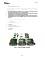
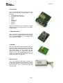
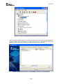
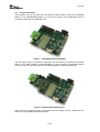
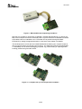
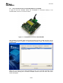
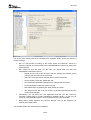
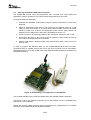
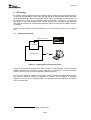
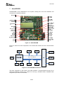
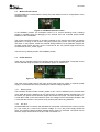
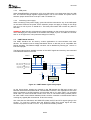
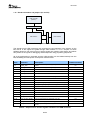
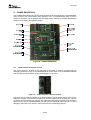
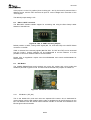
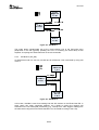
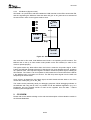
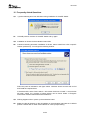
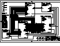
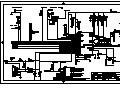
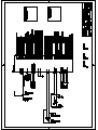
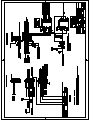
CC2520 Development Kit
User’s Guide
swru138
swru138
Table of contents
1
2
3
4
5
5.1
5.2
5.3
5.4
5.5
6
6.1
6.2
7
7.1
INTRODUCTION ............................................................................................................ 3
ABOUT THIS MANUAL ................................................................................................. 3
ACRONYMS................................................................................................................... 4
DEVELOPMENT KIT CONTENTS................................................................................. 5
GETTING STARTED...................................................................................................... 7
SMARTRF STUDIO ............................................................................................................ 7
INSTALLING SMARTRF STUDIO AND WINDOWS DRIVERS ...................................................... 7
USING THE HARDWARE .................................................................................................... 11
USING SMARTRF STUDIO WITH SMARTRF05EB AND CC2520EM .................................... 13
RUNNING THE SOFTWARE APPLICATION EXAMPLES .......................................................... 15
RF TESTING ................................................................................................................ 16
OUTPUT POWER TESTING ................................................................................................ 16
PACKET ERROR RATE (PER) TESTING ............................................................................. 17
SMARTRF05EB ........................................................................................................... 18
USB MCU...................................................................................................................... 19
7.1.1
7.1.2
Boot loader and standard firmware ................................................................................................................. 19
USB MCU pin out ............................................................................................................................................ 20
MODE SELECTION SWITCH ............................................................................................... 21
POWER SOURCES ........................................................................................................... 21
Battery power .................................................................................................................................................. 21
DC Jack........................................................................................................................................................... 21
USB power ...................................................................................................................................................... 22
Laboratory power supply ................................................................................................................................. 22
UART RS232 INTERFACE ............................................................................................... 22
JOYSTICK ....................................................................................................................... 23
7.2
7.3
7.3.1
7.3.2
7.3.3
7.3.4
7.4
7.5
7.6
7.7
7.8
7.9
7.10
7.11
7.12
8
8.1
8.2
8.3
LCD............................................................................................................................... 23
BUTTONS ........................................................................................................................ 23
LEDS ............................................................................................................................. 23
SERIAL FLASH ................................................................................................................. 23
DEBUG CONNECTORS (P18 AND P20) ............................................................................. 24
EM CONNECTORS ........................................................................................................... 24
BREAK-OUT HEADERS AND JUMPERS (P1 AND P4) ............................................................ 25
CCMSP-EM430F2618 .................................................................................................. 27
JTAG INTERFACE AND POWER SOURCE ............................................................................ 27
BSL OR UART CONNECTOR ............................................................................................ 28
SPI MODES .................................................................................................................... 28
8.3.1
8.3.2
8.3.3
SPI Mode 1 (SPI_M1) ..................................................................................................................................... 28
SPI Mode 2 (SPI_M2) ..................................................................................................................................... 29
SPI Mode 3 (Bypass mode) ............................................................................................................................ 30
9
10
11
12
CC2520EM ................................................................................................................... 30
FREQUENTLY ASKED QUESTIONS ......................................................................... 31
REFERENCES ............................................................................................................. 33
DOCUMENT HISTORY ................................................................................................ 33
2/33
swru138
1
Introduction
Thank you for purchasing a CC2520 Development Kit.
The CC2520 is Texas Instrument’s second generation ZigBee/IEEE 802.15.4 RF transceiver
for the 2.4 GHz unlicensed ISM band. This chip enables industrial grade applications by
offering state-of-the-art noise immunity, excellent link budget, operation up to 125 degrees
and low voltage operation.
In addition, the CC2520 provides extensive hardware support for packet handling, data
buffering, burst transmissions, data encryption, data authentication, clear channel
assessment, link quality indication and packet timing information. These features reduce the
load on the host controller.
The CC2520 Development Kit includes all the necessary hardware in order to properly
evaluate, demonstrate, prototype and develop software targeting not only 802.15.4 or ZigBee
compliant applications, but also proprietary applications requiring a DSSS radio.
Make sure to subscribe to the Low-Power RF eNewsletter to receive information about
updates to documentation, new product releases and more. Sign up on the Texas
Instruments Low Power Wireless web site www.ti.com/lpw.
2
About this manual
This manual contains reference information about the hardware components of the CC2520
Development Kit.
Chapter 4 will briefly describe the contents of the development kit and chapter 5 will give a
quick introduction to how to get started with the kit. In particular, it describes how to install
SmartRF Studio to get the required drivers for the evaluation board, how the hardware can be
used and mentions the software that is available for the development kit. Chapter 6 explains
some simple methods for performing practical RF testing with the development kit. Chapter 7,
8 and 9 describe in detail the hardware that can be found in the kit. A troubleshooting guide
can be found in chapter 10. Appendix A and B contain the schematics for the SmartRF05EB
and CCMSP-EM430F2618 respectively.
The CC2520DK Quick Start Guide (www.ti.com/lit/swru139) has a short tutorial on how to get
started with the kit. The CC2520 Software User’s Guide (www.ti.com/lit/swru137) has details
about the software examples and information about other software options for the CC2520.
The PC tools SmartRF® Studio and SmartRF® Flash Programmer have their own user
manuals.
Please visit the kit web page on www.ti.com/cc2520dk for additional information.
See chapter 11 for a list of relevant documents and links.
3/33
swru138
3
Acronyms
ADC
BSL
DK
EB
EM
FET
IC
JTAG
kB
LCD
LCL
LED
LPW
MCU
PER
RF
RX
SoC
SPI
TI
TX
UART
USB
Analog to Digital Converter
Bootstrap Loader
Development Kit
Evaluation Board
Evaluation Module
Flash Emulation Tool
Integrated Circuit
Joint Test Action Group
Kilo Byte (1024 byte)
Liquid Crystal Display
Local
Light Emitting Diode
Low Power Wireless
Micro Controller
Packet Error Rate
Radio Frequency
Receive
System on Chip
Serial Peripheral Interface
Texas Instruments
Transmit
Universal Asynchronous Receive Transmit
Universal Serial Bus
4/33
swru138
4
Development Kit contents
The CC2520 Development Kit includes hardware and software that allows quick testing of the
CC2520 RF performance and offers a complete platform for development of advanced
prototype RF systems.
•
Evaluate the CC2520 right out of the box. The kit can be used for range testing using the
pre-programmed PER tester running on the MSP430F2618.
•
Use SmartRF Studio to perform RF measurements. The radio can be easily configured to
measure sensitivity, output power and other RF parameters.
•
Prototype development. All I/O from the CC2520 are available on pin connectors on the
SmartRF05EB and on the CCMSP-EM, allowing easy interconnection to other devices or
controllers.
The development kit contains the following components
•
3 x SmartRF®05EB
•
3 x CC2520EM evaluation modules
•
3 x Antennas
•
2 x CCMSP-EM430F2618
•
1 x MSP-FET430UIF debug interface
•
3 x USB cables
•
Documents
Figure 1 - CC2520 Development Kit Contents
5/33
swru138
SmartRF05EB
The SmartRF05EB (Evaluation Board) is the main
board in the kit with a wide range of user
interfaces:
• 3x16 character serial LCD
• Full speed USB 2.0 interface
• UART
• LEDs
• Serial Flash
• Potmeter
• Joystick
• Buttons
The EB is the platform for the evaluation modules
(EM) and can be connected to the PC via USB to
control the EM.
CCMSP-EM430F2618
This is a generic microcontroller board with an
MSP430F2618. The MCU Board can be plugged
into the SmartRF05EB and it is compatible with
most TI LPW RF-IC EMs.
CC2520EM
This is the CC2520 Evaluation Module (EM) with
the RF IC and necessary external components
and matching filters for getting the most out of the
radio. The module can be plugged into the
SmartRF05EB directly for control from SmartRF
Studio or into the CCMSP-EM430F2618 for
control from MSP430. Use the EM as reference
design for antenna and RF layout.
MSP-FET430UIF
This is the MSP430 USB Debug Interface for
programming and debugging applications running
on the MSP430F2618. It connects to the PC via
USB and uses JTAG to communicate with the
microcontroller.
6/33
swru138
5
Getting started
Please refer to the CC2520DK Quick Start Guide (www.ti.com/lit/swru139) for a short
introduction on how to use the kit.
5.1
SmartRF Studio
SmartRF Studio is a PC application developed for configuration and evaluation of many of the
RF-IC products from Texas Instruments, including the CC2520. The application is designed
for use with an applicable SmartRF evaluation board, such as the SmartRF05EB, and runs on
Microsoft Windows.
SmartRF Studio lets you explore and gain knowledge about the CC2520 as it gives you full
overview and access to the RF-IC’s registers to configure the radio and has a control
interface for simple radio operation from your PC.
This means that SmartRF Studio will help radio system designers to easily evaluate the RF-IC
at an early stage in the design process. It also offers a flexible code export function of radio
register settings for software developers.
The latest version of SmartRF Studio can be downloaded from the Texas Instruments website
(www.ti.com/smartrfstudio), where you will also find a complete user manual.
5.2
Installing SmartRF Studio and Windows drivers
Before your PC can communicate with the SmartRF05EB over USB, you will need to install
the driver files for the EB. The latest SmartRF Studio installer includes drivers for Windows.
It is highly recommended to install SmartRF Studio before you
connect the SmartRF05EB to the computer.
A brief set of installation instructions for Microsoft Windows XP will be given here, but also
Windows 2000, Windows NT and Windows 98 are supported. Please consult the SmartRF
Studio User Manual for further details or the troubleshooting section if needed.
After you have downloaded the SmartRF Studio from the web, extract the zip-file, run the
installer file and follow the instructions. Pick a complete installation to include the SmartRF
Studio program, the SmartRF Studio documentation and the necessary Windows drivers
needed to communicate with the SmartRF05EB.
You can now connect your SmartRF05EB to the computer with a USB cable and turn it on. A
“Found New Hardware” dialog box will prompt you to locate the missing driver.
7/33
swru138
Figure 2 - Connecting the SmartRF05EB for the first time (Windows XP)
If you did a complete install of SmartRF Studio, the driver to use is already copied to your
hard drive. Select “No, not this time” and continue with “Next”.
Figure 3 - Select automatic installation of software (Windows XP)
8/33
swru138
Select “Install the software automatically” to install the driver for the SmartRF05EB. Windows
should automatically find the location of the driver to use. If unsuccessful, go back and
manually specify to look in specific location and select the directory C:\Program Files\Texas
Instruments\Extras\Drivers for the needed *.inf and *.sys driver files.
Figure 4 - The driver installation is completed (Windows XP)
The driver is now installed and the computer should be ready for use with SmartRF Studio.
You can verify that the driver is properly installed by opening the Device Manager and see
that when the EB is connected the “Cebal controlled devices” list contains “SmartRF05EB”
and that it is not labelled with an exclamation mark.
9/33
swru138
Figure 5 - Properly installed SmartRF05EB software (Windows XP)
When launching SmartRF Studio, the evaluation board should now appear in the SmartRF05
DK tab. Double click on the device, and a new window opens – giving access to all of the
registers on the chip as well as making it possible to perform various RF test.
Figure 6 - SmartRF Studio with a CC2520EM connected to a SmartRF05EB
10/33
swru138
5.3
Using the hardware
The hardware in the kit can be used in two different modes. Either connect the CC2520EM
directly to the SmartRF05EB (Figure 7) or connect the EM to the CCMSP-EM and then
connect this assembly to the EB (Figure 8).
Figure 7 - CC2520EM and SmartRF05EB
The first option (Figure 7) should be used when the RF Module is controlled by SmartRF
Studio via the USB controller on SmartRF05EB. It is also possible to implement software
running on the microcontroller (CC2511) on SmartRF05EB to control the EM directly.
Figure 8 - EB with EM and MCU board
The second case (Figure 8) can be used when the RF module is to be controlled by the
MSP430 on the CCMSP-EM430F2618 board.
11/33
swru138
Figure 9 - EM and MCU board operating standalone
Note that it is possible to operate the CC2520EM + CCMSP-EM standalone (i.e. without the
EB), but this requires some sort of external power. Figure 9 shows the CC2520EM connected
to the MCU board as a standalone unit. The board can be powered through the MSPFET430UIF by setting the appropriate switch on the board. See chapter 8 for details.
The development kit comes with two CCMSP-EM430F2618 allowing two complete nodes for
peer-to-peer link testing and simple protocol testing. The additional hardware (SmartRF05EB
+ CC2520EM) can be used for debugging purposes, e.g. packet sniffing or capturing and/or
inserting packets using SmartRF Studio.
Figure 10 - Complete set up of development kit hardware
12/33
swru138
5.4
Using SmartRF Studio with SmartRF05EB and CC2520EM
In order to use the SmartRF Studio the CC2520EM is connected directly to the
SmartRF05EB, as shown in the picture below.
Figure 11 - CC2520EM connected to SmartRF05EB
After installation of SmartRF Studio and plugging the EB to the PC via USB, the driver can be
installed as described in chapter 5.2. When starting SmartRF Studio, the following window
should appear:
Make sure you select the tab called SmartRF® 05 DK. The connected evaluation board
should be listed, showing that a CC2520 is available. Double click on the item, and a new
window will appear.
13/33
swru138
This is the main control panel for the CC2520 from SmartRF Studio. It lets you perform a
number of things:
•
Run TX Test modes for testing of RF output power and spectrum. Connect a
spectrum analyser or a power meter to the CC2520EM SMA connector to perform RF
measurements.
•
Run Packet TX and RX tests. For this test, you should have two EBs with
CC2520EMs connected to the PC.
o
Double click on both of the devices in the list, opening two windows, giving
control of the two radios at the same time.
o
Select one to be the receiver and the other to be the transmitter.
o
On the receiver, select the “Packet RX” tab.
o
Set up basic test parameters and press the “Start packet RX” button.
o
On the transmitter, select the “Packet TX” tab.
o
Start transmission by pressing the “Start packet TX” button.
o
The status window will show the number of packets sent/received and the
current signal strength.
•
Alternatively, you can have your own application and test your RX routine by
receiving a packet sent by a radio controlled by SmartRF Studio – or test your TX
routine by using SmartRF Studio to receive packets sent by your application.
•
Read and/or modify registers and common settings, such as RF frequency (or
channel) and output power.
The SmartRF Studio user manual has more details.
14/33
swru138
5.5
Running the Software Application Examples
The CCMSP-EM boards come pre-programmed with a Packet Error Rate (PER) test
application, making it possible to e.g. perform simple range testing out of the box.
Running the PER test application:
1. Assemble the hardware as described in Figure 8 above. Remember to connect the
antennas.
2. Select an appropriate power source. The boards can be powered either via a USB
cable, by using a DC power or by using 2xAA batteries. Make sure that the power
selection jumper P11 chooses the appropriate power source (right position for
batteries, left for USB power or DC power). See details in section 7.3.
3. Power is turned on by switching position of the main power switch from OFF to ON.
4. Follow the instructions on the LCD by using the joystick to select modes and set up
one node as transmitter and one as receiver.
5. When the test starts, it displays a PER value and an RSSI value on the LCD on the
receiver node.
In order to program the MSP430 MCU on the CCMSP-EM430F2618 board the MSPFET430UIF (FET) is needed. Connect the FET to the JTAG connector P12 on the CCMSPEM430F2618 and to a PC with a USB cable. Use IAR Embedded Workbench for MSP430 to
download and debug.
Figure 12 Downloading a new application on the MSP430
The CC2520 Software User’s Guide has details about the available software examples.
Full source code for the software examples can be downloaded from the CC2520DK web
page (www.ti.com/cc2520dk).
Please also visit the TIMAC web-site (www.ti.com/timac) for a complete 802.15.4 compliant
MAC layer for the MSP430F2618 and CC2520 platform.
15/33
swru138
6
RF testing
RF testing is best performed by using SmartRF Studio together with the Development Kit.
Connect the SmartRF05EB to a PC using the USB interface. Start SmartRF Studio and select
the SmartRF05DK tab. Select the evaluation board with the CC2520EM (several boards can
be connected to a PC at once) - it should be listed as “CC2520 – new device” – and click the
start button. In the main SmartRF Studio window settings can be changed, tests performed
and registers adjusted. RF measurement equipment may be connected to the SMA connector
on the EM.
Please see the SmartRF Studio documentation for more information about how to use the
tool.
6.1
Output power testing
50 Ohm coax cable
Spectrum Analyser
CC2520EM
SmartRF05EB
USB
Figure 13 - Output power measurement set up
Instead of connecting an antenna to the SMA connector on the small EM, connect a 50 Ohm
coaxial cable directly to a spectrum analyzer. Use the “TX Test Modes” 1 function in SmartRF
Studio to set up the chip to emit a signal at the desired frequency.
By using good-quality RF cabling, the loss in the cabling should be negligible. However make
sure that the spectrum analyser is calibrated. If possible, check it against a calibrated
instrument such as an RF signal generator. Un-calibrated spectrum analysers can display
errors of several dBs.
1
Use either TXFIFO looping or pseudo random data.
16/33
swru138
6.2
Packet Error Rate (PER) testing
The PER number is the ratio between number of packets being lost and the total number of
packets being sent. PER relates to the more traditional Bit Error Rate (BER) through the
formula
PER = 1 − (1 − BER) packet _ length
The sensitivity threshold of the radio is the lowest input signal strength at which the receiver
can decode the signal with a reasonable degree of correctness. Usually, a PER of 1% is used
as the limit for determining the sensitivity threshold.
It is possible to perform practical range testing with the PER test application which is
preprogrammed on the CCMSP-EM430F2618 boards. Place the transmitter at a fixed location
and place the receiver at a given distance from the transmitter. Then run the PER test to
measure packet errors and possibly the signal strength. Repeat at different distances to get
an idea of the range that can be obtained.
By adding a jammer (a third node that generates either noise on the same channel or a strong
signal on an adjacent channel) it is also possible to measure co-channel rejection and
selectivity/blocking performance.
The same PER test application can be used for simple sensitivity measurements with the
CC2520EM and/or with your own prototype hardware. In this case, connect the unit you want
to test to a known good transmitter with coaxial cables and attenuators. Add more attenuators
until the PER value is 1%. The signal strength at the receiver side is then the sensitivity limit
of the system.
For more information about sensitivity testing, please refer to “DN002 – Practical Sensitivity
Testing” (www.ti.com/lit/swra097).
17/33
swru138
7
SmartRF05EB
SmartRF05EB is the motherboard in the system, hosting all of the user interfaces and
connections to external interfaces.
Figure 14 - SmartRF05EB
Figure 15 shows the main components of the board and outlines the main communication
buses.
Figure 15 - SmartRF05EB architecture
The main component on the board is the USB controller. It communicates with the PC via
USB and translates requests from various PC tools (e.g. SmartRF Studio, SmartRF Flash
Programmer) to actions on the board.
18/33
swru138
The USB controller communicates with the evaluation module using SPI or UART.
Note that not all of the peripherals on the board are accessible from the USB controller. It has
access to the UART RS232 interface, LCD, one LED (D6), joystick and one button (USB
button). I.e. it does not have access to the serial flash on the board.
The module connected to the EM connector has potentially access to all of the EB
peripherals. It has full access to the LCD, serial flash, four LEDs, 2 buttons, joystick and
UART RS232 interface.
Since many of the peripherals can be accessed from both the USB controller and the MCU
EM, some I/O pins can potentially be driven by two different sources. The standard firmware
running on the USB controller handles this by setting all shared I/O in three-state (high
impedance) and thus avoids conflict.
7.1
USB MCU
The USB MCU is the CC2511F32 from Texas Instruments. It is actually a Low Power
Wireless System-on-chip including a state-of-the-art 2.4 GHz radio, 32 kB in system
programmable flash, 4 kB RAM, a 12 bit ADC, timers and a USB controller. Please see
www.ti.com/cc2511 for detailed information about this controller.
7.1.1
Boot loader and standard firmware
The USB controller is programmed with a boot loader when it is shipped from the factory. The
boot loader allows programming of new code into the USB MCU via the USB cable (i.e. no
extra programmer or hardware needed). The boot loader communicates with SmartRF Studio
or SmartRF Flash Programmer.
When the USB controller starts running, it will check for a valid version of firmware in flash. If
it detects a valid application, the boot loader boots the firmware and cedes control of the
controller.
The standard firmware is used to control the RF EM and communicate with applications
running on the PC via USB.
Updating of firmware is done automatically by SmartRF Studio if it detects an old and/or
incompatible firmware version on the controller. SmartRF Studio and SmartRF Flash
Programmer also allow manual programming of the firmware. Please refer to the respective
user’s guides for detailed instructions.
There should not be any EM boards connected to the 05EB while
updating the firmware on the EB.
It is also possible to update the firmware and boot loader on the board by using the debug
interface of the USB Controller. As this is a CC2511, use a SmartRF04EB2 to program the
controller. Connect a 10-pin flat cable to the “Ext SoC Debug” plug (P3) on the SmartRF04EB
and to the “USB Debug” plug (P2) on the SmartRF05EB. Use SmartRF Flash Programmer to
do the actual programming.
Note that there is a way to force the boot loader not to start the firmware. Place the EB Mode
Selection switch in the CC2511JOYSTICK position and move the joystick in any direction
(other than the centre position). When the board is turned on, the firmware is not started and
the boot loader will have control of the board. The LED D6 will be blinking with a 1 second
2
Not included in this kit
19/33
swru138
interval, indicating that the boot loader is running. Use this method to check whether you have
a working boot loader or not.
If the LED D6 blinks with a faster frequency (10 times per second) the boot loader could not
find a valid application to boot.
The same LED will be on when the firmware is running (indicating OK).
When the boot loader is running, the only functionality that is offered from SmartRF Studio
and SmartRF Flash Programmer is to load a new version of the standard firmware.
7.1.2
USB MCU pin out
The following table shows the usage of I/O pins on the USB MCU.
Pin
Function
Description
P0.0
SPI_SELECT /JOY_LEVEL
Function depending on switch P21:
NORMAL: When SPI_SELECT is set LOW, it enables a special CC2520 sniffer
interface (for test and diagnostic purposes.
CC2511JOY: Joystick level is an analog value that can be decoded to find the
actual position of the joystick (centre, up, left, right or down)
P0.1
USB_EM_RESET
Signal used to reset the EM board
P0.2
USB_CS
SPI Chip select for device on EM board
P0.3
USB_SCLK
SPI Clock
P0.4
USB_MOSI
SPI MOSI (master out, slave in)
P0.5
USB_MISO
SPI MISO (master in, slave out)
P1.0
USB_IFC_CTRL
Enables the USB interface when it is set high. Set either by the boot loader or
the firmware.
P1.1
USB_DBG_DC
Debug clock – used when CC2511 communicates with another LPW Soc via
the debug interface.
P1.2
USB_UART_RTS/USB_LED
Dual function: UART Ready To Send and output signal for control of LED D6.
P1.3
USB_UART_CTS/USB_BUTTON
Dual function: UART Clear To Send and input signal for USB button event.
P1.4
USB_UART_TX
UART TX
P1.5
USB_UART_RX
UART RX
P1.6
DGB_DD_DIR /JOY_MOVE
Function depending on switch P21:
NORMAL: The debug data direction signal controls the signal flow on the level
converter for the external debug interface.
CC2511JOY: Joystick move signal input. Set high on any joystick event
(pushed, moved up, left, right or down)
P1.7
USB_DBG_DD
Debug data – used when CC2511 communicates with another LPW SoC via
the debug interface.
P2.0
USB_LCD_FLASH_RESET
Resets both the serial flash and the LCD on the board when it is set low.
P2.1
CC2511 DBG DD
CC2511 debug interface
P2.2
CC2511 DBG DC
CC2511 debug interface
P2.3
LCD_MODE
Selects operating mode of the LCD
P2.4
LCD_CS
SPI Chip select signal for the LCD
Table 1 - USB MCU pin-out
As mentioned in the table, the joystick output is coded as an analogue voltage. This has been
done in order to save the number of pins required on the MCU to interface with the joystick.
20/33
swru138
7.2
Mode selection switch
SmartRF05EB has a mode selection switch (P21) that allows two minor configurations of the
evaluation board.
Figure 16 - EB Mode Selection switch
In the NORMAL position, the evaluation board is in a normal operating mode, enabling
support in hardware both for debugging of an external SoC and a special packet sniffer
interface for the CC2520EM.
The CC2511JOYSTICK position is primarily intended for the special case where a custom
application is running on the CC2511 using the joystick (JOY_LEVEL and JOY_MOVE) for
user input. In this position, neither the external debug interface nor the hardware support for
CC2520 packet sniffer will work. P0.0 is connected to the JOY_MOVE signal and P0.6 is
connected to the JOY_LEVEL signal.
The switch is by default placed in the NORMAL position.
7.3
Power Sources
There are four possible solutions for applying power to the SmartRF05EB. The power source
can be selected using the power source selection jumper on header P11.
Figure 17 - Main power switch and power selection jumper
The main power supply switch (P8) turns off all power sources, unless an external power
supply is connected to the board, overriding the onboard voltage regulators.
7.3.1
Battery power
The evaluation board includes a battery holder for two 1.5V AA batteries on the reverse side
of the PCB: Normal AA batteries can be used and the on board regulator supplies 3.25 V to
the board. The power source selection jumper should short circuit pin 1 and 2 of header P11.
A LOW BATT LED on the board will be lit when the voltage on the board drops beneath 1.56
V. Note that this function is only active when powering the board using batteries.
7.3.2
DC Jack
SmartRF05EB has a connector with standard DC jack power connectors with a 2.5mm centre
pin. The centre pin is used for the positive voltage. A 4-10 V DC power supply should be
used. The onboard voltage regulator supplies approx 3.05 V to the board. The power source
selection jumper should short circuit pin 2 and 3 of header P11.
21/33
swru138
7.3.3
USB power
When SmartRF05EB is connected to a PC via a USB cable, it can draw power from the USB
bus. The onboard voltage regulator supplies approx 3.05 V to the board. The power source
selection jumper should short circuit pin 2 and 3 of header P11.
7.3.4
Laboratory power supply
When connecting a lab power supply, ground should be connected to any of the GND pads
on the board. Remove the power source selection jumper and apply a voltage in the range
from 2.7V to 3.6V to pin 2 on header P11. The main power switch will not have any effect in
this case.
WARNING! Note that this will bypass all voltage regulators on the board so there might be a
risk of damaging the components on the board if the voltage on pin 2 on header P11 is lower
than -0.3V or higher than 3.9V (maximum ratings for CC2511).
7.4
UART RS232 interface
The UART interface can be used by custom applications for communication with other
devices. The interface uses a voltage translation device so that the port is compatible with
RS232 signalling. The RS232 voltage converter can be disabled by shorting pin 1 and 2 on
P10 with a jumper.
The figure below gives a detailed overview of the UART signals and how they are connected
to the different devices on the EB.
CC2511
LED
Button
EM Interface
P1
CC2511 CTS
1-2
RTS
CC2511 RTS
3-4
CTS
USB_UART_RX
CC2511 TX
5-6
RX
USB_UART_TX
CC2511 RX
7-8
TX
USB_UART_RTS
USB_UART_CTS
RTS
CTS
Vcc
RX TX
P10
EN
RS232
Level Converter
GND
P16
Figure 18 - UART RS232 signals and jumpers
As the figure shows, signals are crossed on the EB between the EM and CC2511 and
between the EM and the RS232 level converter/DE9 connector. The implication is that if the
board connected to the EM interface communicates with a PC using UART, use a straight
serial cable. To communicate with CC2511 from a PC, a null-modem cable (crossed) has to
be used. UART communication between CC2511 and the controller on the EM works without
crossing any signals (RX connected to TX and vice versa).
Also note that the USB button and USB LED share the RTS and CTS signals going to the
CC2511. To avoid any conflicts when the RTS/CTS UART flow control signal are used,
disconnect jumpers 1-2 and 3-4 on P1. They are disconnected by default.
22/33
swru138
7.5
Joystick
The joystick detects five positions (centre, up, down, left, right) and one event (pushed). In
case of moving the joystick from its centre position or pushing it, 5 discrete signals can be
used to distinguish what happened. The discrete signals are only available to the
microcontroller on the EM. In addition, two aggregated signals can be used to detect a
joystick event. One signal, JOY_MOVE, is set high in case of any movement away from the
centre position, including pushing. The other signal, JOY_LEVEL, is a voltage level signal that
gives different values depending on the current position of the joystick.
Joystick position
JOY_LEVEL (Volts)
Up
0.31
Down
1.16
Left
1.62
Right
1.81
Centre
2.12
Table 2 - Voltage on JOY_LEVEL for different joystick positions
Measured at T=25°C, Vdd=3.0V
7.6
LCD
The LCD on SmartRF05EB is a 3x16 character display from Hitech Displays (HMC16311).
Use the SPI bus and the additional control signals (LCD CS, LCD Mode and LCD Reset) to
control the LCD.
7.7
Buttons
There are five buttons on the evaluation board.
Button 1 and Button 2 are only connected to the EM, while the USB button is connected to the
USB Controller. There are no RC filters on the buttons.
The USB Reset button resets the USB controller. Note that the USB controller will in turn
reset the EM, so pushing the USB reset button also resets the controller on the EM.
The EM reset button will only result in resetting the controller on the EM (e.g. the
MSP430F2618 on the CCMSP EM).
7.8
LEDs
There are 6 LEDs on the board.
The four LEDs D1, D2, D3 and D4 can only be controlled via the EM.
LED D6 can be controlled by the USB controller.
The LOW BATT LED is turned on when the voltage from the batteries drops below
approximately 1.56V.
7.9
Serial Flash
SmartRF05EB has a M25PE10 flash device – a 1 Mbit (128 Kb × 8 bit) serial paged flash
memory from STMicroelectronics. It can be accessed over the SPI bus from the EM, but not
from the USB Controller, as the latter has not access to the flash chip select signal.
23/33
swru138
7.10 Debug Connectors (P18 and P20)
The debug connectors bring out all the signals from the EM connectors. These connectors
are compatible with Agilent logic analyser probes. The connectors allow easy access to I/O
signals and to connect prototyping boards.
Signal name
Pin
Pin
Signal name
NC
1
2
NC
NC
3
4
EM_FLASH_CS
EM_BUTTON1
5
6
EM_LED1
EM_UART_RX
7
8
EM_JOYSTICK_RT
EM_UART_TX
9
10
EM_DBG_DD
EM_LCD_MODE
11
12
EM_DBG_DC
EM_LCD_FLASH_RESET
13
14
EM_CS
EM_JOY_LEVEL
15
16
EM_SCLK
EM_POT_R
17
18
EM_MOSI
EM_MISO
19
20
GND
Table 3 - I/O connector P18 pin-out
Signal name
Pin
Pin
Signal name
NC
1
2
NC
NC
3
4
EM_LED2
PS_PWR_SNOOZE
5
6
EM_LED2
EM_VCC
7
8
EM_LED4
NC
9
10
EM_JOYSTICK_PUSH
EM_JOYSTICK_UP
11
12
EM_JOYSTICK_DN
EM_JOYSTICK_LT
13
14
EM_UART_CTS
EM_RESET
15
16
EM_BUTTON2
EM_LCD_CS
17
18
EM_UART_RTS
EM_JOY_MOVE
19
20
GND
Table 4 - I/O connector P20 pin-out
7.11 EM connectors
The EM connectors are used for connecting the EM to the SmartRF®05EB. The connectors
P5 and P6 are used as the main interface.
24/33
swru138
7.12 Break-out headers and jumpers (P1 and P4)
USB Controller
(CC2511)
P4 Jumpers
P1 Jumpers
EM Interface
User Interface
Figure 19 - Basic signal flow on the evaluation board
The signals from the EM connectors are connected to user interfaces or the CC2511 on the
EB, but all of the signals are gated through either header P1 or P4. Jumpers on these
headers allows for fine tuned control of which signals are routed to what device and allows
easy break-out of signals for debugging and development using proprietary peripherals.
All of the peripherals on the board and the USB controller can be isolated entirely from the
EM, facilitating accurate power consumption measurements.
Pins
Function
Description
Default mounted
1-2
UART_RTS
Ready to send – for systems supporting hardware flow
control
No
3-4
UART_CTS
Clear to send – for systems supporting hardware flow control
No
5-6
UART_RX
Received data- connected to TX on CC2511
Yes
7-8
UART_TX
Transmitted data – connected to RX on CC2511
Yes
9-10
SNIFF_DATA
Sniff interface – bit stream of data from radio
No
11-12
SNIFF_CLK
Sniff interface – clock for data sampling
No
13-14
SNIFF_MISO
Sniff interface – not used
No
15-16
SNIFF_SFD
Sniff interface – start of frame delimiter from
No
17-18
DBG_DC
Debug Clock signal (debug interface for system-on-chips)
Yes
19-20
DBG_DD
Debug Data signal (debug interface for system-on-chips)
Yes
21-22
CS
Chip select for SPI device on EM module
Yes
23-24
SCLK
SPI clock
Yes
25-26
MOSI
SPI data – master output, slave input
Yes
27-28
MISO
SPI data – master input, slave output
Yes
29-30
LCD_CS
Chip select for LCD
Yes
31-32
LCD_MODE
LCD control signal
Yes
33-34
LCD_FLASH_RESET
Common reset signal for serial Flash and LCD
Yes
35-36
JOY_LEVEL
Voltage level from joystick, indicating position
Yes
JOY_MOVE
There is a positive edge on this signal when the joystick is
moved
Yes
37-38
Table 5 - Jumpers on P1. Control signals available to the USB controller.
25/33
swru138
Pins
Function
Description
Default mounted
1-2
JOY_MOVE
See P1, 37-38
Yes
3-4
JOY_LEVEL
See P1, 35-36
Yes
5-6
LCD_FLASH_RESET
See P1, 33-34
Yes
7-8
LCD_MODE
See P1, 31-32
Yes
9-10
LCD_CS
See P1, 29-30
Yes
11-12
MISO
See P1, 27-28. Connected to LCD and serial Flash.
Yes
13-14
MOSI
See P1, 25-26. Connected to LCD and serial Flash.
Yes
15-16
SCLK
See P1, 23-24. Connected to LCD and serial Flash.
Yes
17-18
FLASH_CS
Chip select for serial flash
Yes
19-20
BUTTON1
Button 1. Low when pushed.
Yes
21-22
BUTTON2
Button 2. Low when pushed.
Yes
23-24
LED1
Control signal for LED D1. Set high to turn LED on.
Yes
25-26
LED2
Control signal for LED D2. Set high to turn LED on.
Yes
27-28
LED3
Control signal for LED D3. Set high to turn LED on.
Yes
29-30
LED4
Control signal for LED D4. Set high to turn LED on.
Yes
31-32
JOYSTICK_UP
Signal goes high when joystick is moved up.
Yes
33-34
JOYSTICK_DN
Signal goes high when joystick is moved down.
Yes
35-36
JOYSTICK_LT
Signal goes high when joystick is moved left.
Yes
37-38
JOYSTICK_RT
Signal goes high when joystick is moved right.
Yes
39-40
JOYSTICK_PUSH
Signal goes high when joystick is pushed.
Yes
41-42
POT_R
Voltage level from potentiometer. Value between 0 and VCC.
Yes
EM_RESET
Reset signal to EM. Set either by the USB controller or as a
result of pushing the EM reset button.
Yes
43-44
Table 6 - Jumpers on P4. IO signals from all of the peripherals on the evaluation board.
26/33
swru138
8
CCMSP-EM430F2618
The CCMSP-EM430F2618 is a generic MCU board that can be plugged into a SmartRF05EB,
giving access to all of that board’s user interfaces. Any TI LPW transceiver EM, or even a
system-on-chip EM, can be plugged into the MCU board, enabling a versatile development
platform for RF testing and software design.
Figure 20 - CCMSP-EM430F2618
8.1
JTAG interface and power source
The JTAG connector, located on the right side of the board, is used for programming and
debugging software running on the MSP430F2618. Please refer to the CC2520DK Software
User’s Guide for further details on how the debugger can be used.
Figure 21 - JTAG and power selection jumper
The power source selection header (P14) allows selection of what power source to use for the
MSP430 controller. If the selection jumper is in the FET position (short circuiting pin 2 and 3)
the board can be powered from the FET tool. Note that if the board is already powered from a
second source (e.g. the SmartRF05EB), you will have two separate power sources. To avoid
damage of the board, only use FET power if the board is not already powered.
27/33
swru138
If the jumper is in the LCL position (short circuiting pin 1 and 2), the board is powered from a
different source, and the FET uses that as input for correct voltage level conversion of the
JTAG signals.
The default jumper setting is LCL.
8.2
BSL or UART connector
The BSL/UART header enables support for accessing and using the Boot Strap Loader
features of the MSP430.
Figure 22 - BSL or UART selection jumpers
Default position is UART, routing UART signal (RX, TX, CTS and RTS) to the UART RS232
connector on the EB.
If BSL is selected, the necessary signals (BSL RX, BSL TX, RST and TST) can be accessed
from the CC2511. Custom software can be implemented to use the features. It is also
possible to connect an external cable to access the BSL.
Please refer to application reports www.ti.com/lit/slaa089 and www.ti.com/lit/slaa096 for
further details.
8.3
SPI Modes
The CCMSP-EM430F2618 board supports two major SPI modes and a third mode that
enables a particular “bypass” mode. The SPI mode is selected with jumpers on header P9.
Figure 23 - SPI Mode selection header
8.3.1
SPI Mode 1 (SPI_M1)
This is the default SPI mode and uses two separate SPI busses. One is dedicated for
communication with the EM module and the other is dedicated to all the SPI devices on the
EB. The MSP430 uses the internal serial interface USCIB1 for the EM and USCIB0 for the
EB. Se figure below for details.
28/33
swru138
Figure 24 - SPI Mode 1
This mode allows uninterrupted use of the communication bus to the EM while using
peripherals on the EB (typically updating the LCD or accessing the serial flash) at the
expense of requiring two serial interfaces on the microcontroller.
8.3.2
SPI Mode 2 (SPI_M2)
An alternative mode is to use only one SPI bus for all devices. This is achieved by using SPI
mode 2.
Figure 25 - SPI Mode 2
In this case, USCIB0 is used for accessing both the SPI devices on the EB and the EM. In
some cases, this might complicate software, as it needs to make sure ongoing SPI
transactions are not interrupted prematurely (e.g. interrupt from radio triggers reading from
the transceiver using the SPI bus while the MCU is in the middle of writing to the LCD).
29/33
swru138
8.3.3
SPI Mode 3 (Bypass mode)
SPI Mode 3 is a particular mode that enables the USB controller on the EB to access the EM,
and thus bypassing the MSP430. Note that either SPI_M1 or SPI_M2 has to be selected at
the same time in order for the bypass mode to work.
Figure 26 - SPI Mode 3
Also note that in this mode, both MSP430 and CC2511 are operating as SPI masters. The
MSP430 has to set up in multi master mode (enable 4 wire SPI interface) in order for the
mode to operate properly.
The bypass mode only takes effect when the CC2511 assert the chip select signal. At this
instant, the MSP430 will detect that the CS signal goes low, thus releasing the bus, operating
as a passive slave. This chip select signal is routed to the EM chip select signal, enabling its
SPI interface. The CC2511 can now operate as SPI master and communicate with the EM as
if the MSP430 was not present on the bus. The EM chip select signal from the MSP will
temporarily be disconnected.
Once CC2511 de-asserts the chip select signal, the MCU board switches back to one of the
chosen SPI modes (SPI_M1 or SPI_M2).
This mode can be particularly handy for debugging purposes. While debugging software on
the MSP430 and using the RF EM, it is possible to halt the MSP430 application (e.g. at a
breakpoint) and use SmartRF Studio to read out the registers from the radio – without
interfering with the application.
9
CC2520EM
Please refer to the reference design on the web and a description of the evaluation module in
the CC2520 Datasheet.
30/33
swru138
10 Frequently Asked Questions
Q1
I get the following error from Windows during installation of SmartRF Studio:
A1
Uninstall previous versions of SmartRF Studio and try again.
Q2
Installation of drivers for the evaluation board fails.
A2
Instead of selecting automatic installation of drivers, select “Install form a list or specific
location (Advanced)”. You will get the following window.
Select the path as indicated in the figure above. Windows should now be able to find
and install the required driver.
If the above fails, select “Don’t search. I will choose the driver to install.” A new window
will open, asking for a location of where drivers can be found. Select “C:\Program
Files\Texas Instruments\Extras\Drivers\srf05eb.inf”.
Q3
Nothing happens when I power up the evaluation board.
A3
Make sure that all jumpers on the IO headers on the evaluation board are set in default
position. Please refer to Table 5 and Table 6 for correct jumper setting.
31/33
swru138
Q4
The MSP-FET430UIF should be able to power the CCMSP-EM and SmartRF05EB
when connected to the JTAG connector, but it doesn’t seem to work. Why?
A4
Place the jumper on header P14 in position FET (short circuiting pin 2 and 3).
Q5
When powering up the evaluation board, the LED D6 starts blinking. Why?
A5
If the blink frequency is 1 time per second, the boot loader has entered a forced boot
recovery mode (set during programming of the device). Power off the system and turn it
back on to start the application.
If the blinking is more rapid (10 times per second) the boot loader could not find a valid
application in flash. Use SmartRF Studio or SmartRF Flash Programmer to program a
new firmware on the board.
Q6
How can I measure the current consumption of the radio on the EM?
A6
The easiest way to measure current consumption of the chip in various modes is to
connect the EM directly to the SmartRF05EB and disconnect everything on the board
that consumes power by removing all jumpers on P1 and P4. The only jumpers needed
on P1 are the four SPI signals (CS, SCLK, MISO and MOSI) and one for the CC2520
VREG enable signal (DBG_DD). On P4, only the jumper for the EM_RESET signal is
required. Set the jumper on header P10 in position 1-2 (disable RS232 level converter)
and remove jumpers on P13, P14 and P19. Connect the ampere meter between the two
pins on P15 (V_EM).
Use SmartRF Studio to set the radio in different modes (RX, TX, etc.).
The same approach can be used when powering the CCMSP-EM + CC2520EM from
the EB. In this case, only the jumper for the EM_RESET signal on P4 is required.
32/33
swru138
11 References
[1] CC2520DK Quick Start Guide
www.ti.com/lit/swru139
[2] CC2520DK website
www.ti.com/cc2520dk
[3] CC2520 Software Examples User’s Guide
www.ti.com/lit/swru137
[4] CC2520 website
www.ti.com/cc2520
[5] SmartRF Studio
www.ti.com/smartrfstudio
[6] TIMAC
www.ti.com/timac
[7] DN002 -- Practical Sensitivity Testing
www.ti.com/lit/swra097
12 Document history
Revision
Date
-
2007-12-18
Description/Changes
First revision.
33/33
swru138
Appendix A
SmartRF05EB Schematics
swru138
Appendix B
CCMSP-EM430F2618
Schematics
IMPORTANT NOTICE
Texas Instruments Incorporated and its subsidiaries (TI) reserve the right to make corrections, modifications, enhancements,
improvements, and other changes to its products and services at any time and to discontinue any product or service without notice.
Customers should obtain the latest relevant information before placing orders and should verify that such information is current and
complete. All products are sold subject to TI’s terms and conditions of sale supplied at the time of order acknowledgment.
TI warrants performance of its hardware products to the specifications applicable at the time of sale in accordance with TI’s
standard warranty. Testing and other quality control techniques are used to the extent TI deems necessary to support this
warranty. Except where mandated by government requirements, testing of all parameters of each product is not necessarily
performed.
TI assumes no liability for applications assistance or customer product design. Customers are responsible for their products and
applications using TI components. To minimize the risks associated with customer products and applications, customers should
provide adequate design and operating safeguards.
TI does not warrant or represent that any license, either express or implied, is granted under any TI patent right, copyright, mask
work right, or other TI intellectual property right relating to any combination, machine, or process in which TI products or services
are used. Information published by TI regarding third-party products or services does not constitute a license from TI to use such
products or services or a warranty or endorsement thereof. Use of such information may require a license from a third party under
the patents or other intellectual property of the third party, or a license from TI under the patents or other intellectual property of TI.
Reproduction of TI information in TI data books or data sheets is permissible only if reproduction is without alteration and is
accompanied by all associated warranties, conditions, limitations, and notices. Reproduction of this information with alteration is an
unfair and deceptive business practice. TI is not responsible or liable for such altered documentation. Information of third parties
may be subject to additional restrictions.
Resale of TI products or services with statements different from or beyond the parameters stated by TI for that product or service
voids all express and any implied warranties for the associated TI product or service and is an unfair and deceptive business
practice. TI is not responsible or liable for any such statements.
TI products are not authorized for use in safety-critical applications (such as life support) where a failure of the TI product would
reasonably be expected to cause severe personal injury or death, unless officers of the parties have executed an agreement
specifically governing such use. Buyers represent that they have all necessary expertise in the safety and regulatory ramifications
of their applications, and acknowledge and agree that they are solely responsible for all legal, regulatory and safety-related
requirements concerning their products and any use of TI products in such safety-critical applications, notwithstanding any
applications-related information or support that may be provided by TI. Further, Buyers must fully indemnify TI and its
representatives against any damages arising out of the use of TI products in such safety-critical applications.
TI products are neither designed nor intended for use in military/aerospace applications or environments unless the TI products are
specifically designated by TI as military-grade or "enhanced plastic." Only products designated by TI as military-grade meet military
specifications. Buyers acknowledge and agree that any such use of TI products which TI has not designated as military-grade is
solely at the Buyer's risk, and that they are solely responsible for compliance with all legal and regulatory requirements in
connection with such use.
TI products are neither designed nor intended for use in automotive applications or environments unless the specific TI products
are designated by TI as compliant with ISO/TS 16949 requirements. Buyers acknowledge and agree that, if they use any
non-designated products in automotive applications, TI will not be responsible for any failure to meet such requirements.
Following are URLs where you can obtain information on other Texas Instruments products and application solutions:
Products
Applications
Amplifiers
amplifier.ti.com
Audio
www.ti.com/audio
Data Converters
dataconverter.ti.com
Automotive
www.ti.com/automotive
DSP
dsp.ti.com
Broadband
www.ti.com/broadband
Interface
interface.ti.com
Digital Control
www.ti.com/digitalcontrol
Logic
logic.ti.com
Military
www.ti.com/military
Power Mgmt
power.ti.com
Optical Networking
www.ti.com/opticalnetwork
Microcontrollers
microcontroller.ti.com
Security
www.ti.com/security
RFID
www.ti-rfid.com
Telephony
www.ti.com/telephony
Low Power
Wireless
www.ti.com/lpw
Video & Imaging
www.ti.com/video
Wireless
www.ti.com/wireless
Mailing Address: Texas Instruments, Post Office Box 655303, Dallas, Texas 75265
Copyright © 2007, Texas Instruments Incorporated
Mouser Electronics
Authorized Distributor
Click to View Pricing, Inventory, Delivery & Lifecycle Information:
Texas Instruments:
CC2520DK