1
Interferometric Optical Testing for High
Resolution Imaging in an Optical Lattice
TOUT WANG
Department of Physics
University of Toronto
Supervised by Joseph Thywissen
May - September 2008
Abstract
This report describes an interferometric optical testing project aimed at contributing to the construction of a high resolution imaging system for resolving
individual sites in an optical lattice. It begins with a background discussion,
touching upon the relationship between optical distortions and imaging resolution, the motivation for imaging individual sites in an optical lattice, and
popular methods of interferometric optical testing. This is followed by a detailed description of the components of the actual experiment, with an extra
emphasis on the laser diode and the CCD camera. Finally, the report outlines
the Fourier transform method of interferogram analysis and presents a successful calculation of the wavefront distortions resulting from light passing through
various interferometer test objects.
List of Figures
1.1
1.2
1.3
Wavefront Distortions Due to an Optical Window . . . . . . . . .
Geometric Representation of Aberrations . . . . . . . . . . . . .
Interferometer Configurations for Optical Testing . . . . . . . . .
2.1
2.2
2.3
2.4
2.5
2.6
2.7
2.8
2.9
Overview of Experiment Components . . . . . .
Laser Diode Pin Configuration . . . . . . . . . .
Laser Diode Mount . . . . . . . . . . . . . . . . .
Sharp Laser Diode Emission Spectrum . . . . . .
Coherence Considerations . . . . . . . . . . . . .
Power Meter Non-uniformity . . . . . . . . . . .
Beam Shaping Optics Prior to the CCD Camera
Demonstration of Varying Fringe Visibility . . .
Mounting Optical Components for Testing . . . .
.
.
.
.
.
.
.
.
.
.
.
.
.
.
.
.
.
.
.
.
.
.
.
.
.
.
.
.
.
.
.
.
.
.
.
.
.
.
.
.
.
.
.
.
.
.
.
.
.
.
.
.
.
.
11
11
12
13
14
16
18
19
19
3.1
3.2
3.3
3.4
3.5
3.6
3.7
3.8
3.9
Fourier Spectrum of the Transformed Interferogram . .
Fourier Transform of an Interferogram in MATLAB . .
Plot of the Wrapped Phase Function . . . . . . . . . . .
Error in Phase Unwrapping . . . . . . . . . . . . . . . .
Wrapped Phase Function in a Smaller Region of Interest
Successful Unwrapping of a Phase Function . . . . . . .
Plot of a Single Row in the Wrapped Phase Function . .
Plot of a Single Row in the Unwrapped Phase Function
Effect of Errors in Defining the Side Peak . . . . . . . .
.
.
.
.
.
.
.
.
.
.
.
.
.
.
.
.
.
.
.
.
.
.
.
.
.
.
.
.
.
.
.
.
.
.
.
.
.
.
.
.
.
.
.
.
.
23
24
25
26
26
27
28
28
29
A.1 PixelFly Camera Interface Box . . . . . . . . . . . . . . . . . . .
A.2 PyCamera User Interface . . . . . . . . . . . . . . . . . . . . . .
34
37
1
.
.
.
.
.
.
.
.
.
.
.
.
.
.
.
.
.
.
.
.
.
.
.
.
.
.
.
6
7
9
Contents
Acknowledgements
3
Introduction
4
1 Background
1.1 Effect of Wavefront Distortions . . . . . . . . . . . . . . . . . . .
1.2 Imaging Single Atoms in an Optical Lattice . . . . . . . . . . . .
1.3 Interferometric Testing Methods . . . . . . . . . . . . . . . . . .
5
5
8
8
2 Experiment Components
2.1 Powering a 405 nm Laser Diode . . .
2.2 Laser Diode Spectral Characteristics
2.3 Dielectric Mirrors . . . . . . . . . . .
2.4 Remaining Optical Components . . .
2.5 CCD Camera . . . . . . . . . . . . .
2.6 Early Experiments . . . . . . . . . .
.
.
.
.
.
.
.
.
.
.
.
.
.
.
.
.
.
.
.
.
.
.
.
.
.
.
.
.
.
.
.
.
.
.
.
.
.
.
.
.
.
.
.
.
.
.
.
.
.
.
.
.
.
.
.
.
.
.
.
.
.
.
.
.
.
.
.
.
.
.
.
.
.
.
.
.
.
.
.
.
.
.
.
.
10
10
12
15
15
17
17
3 Interferogram Analysis
3.1 Survey of Popular Approaches . . . . . . .
3.2 Fourier Transform Method . . . . . . . . .
3.3 Implementation in MATLAB . . . . . . .
3.4 Discussion of Results . . . . . . . . . . . .
3.5 Possible Errors in Interferogram Analysis
.
.
.
.
.
.
.
.
.
.
.
.
.
.
.
.
.
.
.
.
.
.
.
.
.
.
.
.
.
.
.
.
.
.
.
.
.
.
.
.
.
.
.
.
.
.
.
.
.
.
.
.
.
.
.
.
.
.
.
.
.
.
.
.
.
21
21
22
23
25
27
.
.
.
.
.
.
.
.
.
.
.
.
4 Future Directions
30
A PixelFly Camera Notes
A.1 Software Installation Issues . .
A.2 Hardware Triggering . . . . . .
A.3 Summary of Camera Programs
A.4 Interferometric Optical Testing
A.5 Imaging of Trapped Atoms . .
Bibliography
.
.
.
.
.
.
.
.
.
.
.
.
.
.
.
.
.
.
.
.
.
.
.
.
.
.
.
.
.
.
.
.
.
.
.
.
.
.
.
.
.
.
.
.
.
.
.
.
.
.
.
.
.
.
.
.
.
.
.
.
.
.
.
.
.
.
.
.
.
.
.
.
.
.
.
.
.
.
.
.
.
.
.
.
.
.
.
.
.
.
.
.
.
.
.
33
33
33
34
36
36
39
2
Acknowledgements
I had the pleasure of interacting with each member of the group over the course
of the summer. Marcius repeatedly provided useful advice in matters of camera
programming. Dylan and Dave, the two graduate students in this half of the
lab, continuously challenged me with thought-provoking questions about what
I was doing. Although Jason, Lindsay, and Alma spent most of their day next
door, I had to call upon each of them at one time or another, whether it was
about finding a missing optical component or asking how to go about setting
up new pieces of the experiment. Julie and Michael were my fellow summer
students, and the rapport between the three of us made lab work more enjoyable. Both of them have the privilege of continuing their efforts towards an
undergraduate thesis. I’m also grateful to Alan for the occasions when he took
the time to explain to me how one should do electronics work properly. Final
thanks go to Joseph, for challenging me with this project, teaching me numerous
experimental skills that will no doubt serve me well as a graduate student, and
allowing me to turn part of his lab into an optical testing experiment.
This work was funded by the Natural Sciences and Engineering Research
Council of Canada (NSERC).
3
Introduction
I had several goals for my final summer prior to starting graduate school. I
wanted, of course, to have as much fun as possible before the inevitable pressures
of studying for a Ph.D. I thought it might also be a good idea to keep my mind
sharp by doing an interesting research project, and so I tried, with obvious
success, to get a position in the Ultra-Cold Atoms Lab led by Joseph Thywissen.
Finally, I decided that it would be to my advantage if I could get some practice
with computer programming over the summer months, because it had been
a while since I had thought seriously about programming problems and these
skills will no doubt be vital to doing physics research. In the end, it turned out
to be a minor miracle that I was able to accomplish all these goals with the
work described in this report, because at first glance they would appear to be
mutually exclusive!
The remainder of this report presents my two main contributions to the
experimental efforts in the lab. First, as the title suggests, I made progress
towards high resolution of imaging of individual atoms in an optical lattice
by constructing an interferometer to test wavefront distortions in the imaging
system optical components. In addition to this, I was also responsible for programming the two new CCD cameras in the lab to work with existing image
processing software. One of these cameras is in place on the atom trapping side
of things, ready for imaging both the contents of our magneto-optical trap and
also colder atoms down the road. The other camera is serving dutifully on the
interferometer optics table, where it captures interferograms for computer analysis. The project culminated in a successful proof-of-concept analysis of optical
window interferograms, producing both a phase profile plot and a measure of
the root-mean-square wavefront distortion introduced by the windows.
4
Chapter 1
Background
In this chapter I will present the basic background information necessary to
understand the aim of the project - interferometric optical testing for high resolution imaging in an optical lattice. Topics include how wavefront distortions
affect the resolution of an imaging system, the motivation for site-resolved imaging in an optical lattice, and key concepts in using interferometers to test the
quality of optical components.
1.1
Effect of Wavefront Distortions
In the idealized geometric model of optics, perfect imaging systems have infinite
resolving ability because a cone of light rays emitted from one geometric point
on an object can be brought to focus at another geometric point on the image.
However, due to the wave nature of light, and in particular due to diffraction
effects, no imaging system can take light from one point to another. This
sets a fundamental resolution limit that depends on the wavelength of light
used. For a microscope with numerical aperture N A and light at wavelength
λ, the resolution limit R is defined as the minimum separation that can be
distinguished
λ
R∼
(1.1)
NA
and the minimum value of R, called the diffraction limit, is on the order of a
wavelength of light λ. A thorough analysis of image formation in microscopes
can be found in §8.6.3 of [1].
But this is still in the case of perfect optical components. In practice, imperfections in the imaging optics will cause additional aberrations in the form
of distortions to the the wavefront emerging from the source (Fig. 1.1). The
full treatment of the diffraction theory of aberrations is included in Chapter 9
of [1], but for our purposes it is sufficient to appreciate that wavefront distortions directly impact imaging resolution. The simplest way to understand this
is to return to the geometric picture (Fig. 1.2). Wavefront distortions in the
5
Figure 1.1: Illustration of how the presence of an optical window can introduce
distortions to wavefronts emerging from a diffraction limited point source. When
traced back, the apparent source of these distorted wavefronts is no longer a
diffraction limited point
form of, for example, spherical aberrations will increase the apparent size of
the source from a geometrical point to some finite spot. Interestingly, in the
case of spherical aberrations there is a ‘circle of least confusion,’ which is the
minimum such spot size along the optical axis (see p. 238 of [1]). The location
of this circle of least confusion is off-focus, meaning that if an imaging system
contains spherical aberrations, its resolving ability may be improved by going
slightly out-of-focus (this has been experimentally applied in the imaging of a
single atom in an optical dipole trap [2]).
It is obvious how this simple geometric understanding of the effect of aberrations on imaging resolution can be extended when considering the wave properties of light. If perfect wavefronts from a diffraction-limited point are distorted
(Fig. 1.1), the geometric light rays which represent the direction of propagation
of the distorted wavefront no longer trace back to an apparent source that is a
diffraction-limited spot. Our resolution limit R will then increase, which means
that the resolution of the imaging system has become worse.
Thus far, the explanation of how wavefront distortions affect imaging resolution has been an intuitive one. A quantitative measure of the dependence
of resolution on wavefront distortion involves a parameter known as the Strehl
ratio (see §9.1 of [1] and §3.2 of [3]). The Strehl ratio is defined as
Is = Id /I0
In this definition we consider the diffraction pattern of light from an idealized
point source after passing through some optical system. I0 is defined as the
6
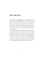
Figure 1.2: Geometrical representation of aberrations in an optical system. (left)
Consider a cone of light rays emerging from a point source. (right) Suppose that
the presence of an optical window after the point source introduces spherical
aberrations into the system, meaning that light rays emerging from different
points on the window have their apparent foci at different locations along the
optical axis when traced back. Since this apparent source of light rays is no
longer a geometric point, the resolution of any image formed from the distorted
light rays will obviously suffer.
peak intensity in the Airy pattern for perfect optical components, while Id is
the measured peak intensity for the actual distorted wavefronts. As the central
spot size of the diffraction pattern increases, the resolution limit also increases,
but the peak intensity must decrease to conserve power. Thus, if Is = 1 then
the system is at the resolution limit described in Equation 1.1. As the Strehl
ratio Is decreases from this maximum value of 1, the resolution limit of the
optical system increases. In the case of small wavefront distortions, the Strehl
ratio Is can be related to the root-mean-square wavefront distortion ∆φrms by
Equation 24 in §9.1 of [1]
Is ≈ 1 − (
2π 2
) (∆φrms )2
λ
(1.2)
A popular standard for imaging quality is the Marechal criterion, which requires
Is > 0.8 or correspondingly ∆φrms < λ/14.
The preceding discussion demonstrates that the root-mean-square measure
of wavefront distortion ∆φrms can be meaningfully related to imaging resolution. This makes it a superior measure of optical quality compared to peak-tovalley (P-V) wavefront distortion, because an imaging system with higher P-V
distortions can still be superior to another with lower P-V distortions if the
larger amplitude distortions are isolated to small regions of the wavefront. The
section on the ‘Star Test’ in [6] presents a visual test of optical quality using
the Strehl ratio which does not require the calculation of the root-mean-square
phase distortion ∆φrms .
7
1.2
Imaging Single Atoms in an Optical Lattice
An optical lattice is formed by interfering pairs of laser beams to create a standing wave. Since atoms interact with electromagnetic fields through dipole forces,
an optical lattice is basically a periodic potential for atoms. An overview of the
motivations behind studying atoms in optical lattices can be found by referring
to [4]. The attraction of working with optical lattices is that they effectively
simulate a simple condensed matter system. On the other hand, experimental
parameters in optical lattices can be controlled much more easily than their
counterparts in condensed matter systems. This makes the optical lattice a
promising test-bed for proposed solutions to the big questions in condensed
matter physics, for example high temperature superconductivity. Conversely
they can also provide clear experimental clues that point the way towards explaining these same theoretical problems.
One of the big goals in the field is to be able to resolve single sites in an
optical lattice with period less than 1 µm. This distance scale is important
because interactions between atoms in neighbouring sites get stronger as the
lattice dimensions decrease, and these interactions are at the core of interesting condensed matter phenomena that experiments with optical lattices aim to
produce and probe. However, at these lattice separations, the goal of resolving individual sites is made especially challenging because the distance scales
in question are right at the diffraction limit for visible light described in §1.1.
So far, the smallest lattice separation that has been resolved is around 5 µm
[5], and efforts to push on towards sub-µm lattice resolution require imaging
systems with extraordinarily low levels of distortions.
1.3
Interferometric Testing Methods
The fundamental principle behind interferometric optical testing is that when
two light beams are interfered with one another, the resultant intensity profile
is an indication of their relative phase. If the two interfering beams are derived
from a single light source, and we place an optical component in the path of
one of the beams, the resulting interference pattern becomes a measure of the
wavefront distortions introduced by the component under testing. Two good
references for interferometric optical testing are [6] and [7]. I will not describe
the basic concepts that are already clearly explained in these books. Instead, I
will comment on some of the practical issues surrounding the common interferometer configurations (Fig. 1.3).
The Twyman-Green interferometer is perhaps the most familiar configuration because it is simply a modified Michelson interferometer. The beam with
the distorted wavefront is formed by light transmitted through the test object,
reflected by the end mirror and then transmitted through the test object a second time. For a transparent component such as an optical window, the final
beam intensity is close to the original intensity, meaning that spurious interference patterns formed by internal reflections within the test object itself have
8
Figure 1.3: The two most common interferometer configurations for optical
testing. (left) The Twyman-Green configuration is basically a Michelson interferometer with a test object such as an optical window inserted in one of the
arms. (right) The Fizeau interferometer contains all the optics in a single arm,
and relies on single reflections from the reference and test objects to form the
two interfering beams.
negligible effect on the overall interferogram. The main disadvantage of this
configuration is that another mirror is required along the optical path beyond
the test object. If the interferometer is used to test distortions due to a vacuum
deflected window (see §3.4 of [3]), it would not be feasible to place another
mirror within the vacuum chamber itself because proper alignment would be
difficult, to say the least.
On the other hand, the Fizeau interferometer is ideal for vacuum testing
because the final element along the optical path is the test object itself. The
reference beam, obtained from a single reflection from the reference object, interferes with another reflected beam from the test object. Immediately a major
problem becomes apparent - each object, assuming they are flat, produces two
reflections from each of its two surfaces. This gives four interfering beams, not
two. Experimentally, two obvious solutions exist. One is to coat the object
surfaces so that one of the two surface reflections becomes dominant. The other
solution is to place the two objects very close together, and use a low coherence
length light source such that the only two reflections capable of producing interference are those from the two adjacent surfaces. Unfortunately it was not
possible to implement either solution in the project. However, §2.6 does contain
some brief descriptions of experimental attempts at doing interferometry in the
Fizeau configuration.
9
Chapter 2
Experiment Components
This next chapter will provide detailed descriptions of the components of the
interferometric optical testing experiment (Fig. 2.1). These are used to set-up
an interferometer in the Twyman-Green configuration, although some attempts
at realizing the Fizeau configuration are also mentioned. The test wavelength
is 405 nm, which is on the violet end of the visible spectrum. It was chosen to
coincide with the planned imaging wavelength in the optical lattice experiment
[3]. Laser diodes at this wavelength are a fairly recent development, so I have
included a thorough discussion of issues involved in powering the diode as well
as careful considerations of its emission properties, which are important towards
interferometric optical testing.
2.1
Powering a 405 nm Laser Diode
The light source for the experiment is a Sharp GH04020A2GE laser diode with
emission wavelength around 405 nm and output power of 20 mW. This diode
sits on a ThorLabs LDM21 laser diode mount, which contains a thermo-electric
cooler (TEC) to regulate the laser diode temperature. The laser diode pin
configuration (Fig. 2.2) is a nonstandard one, and is not compatible with the
interface sockets on the LDM21 (Fig. 2.3) regardless of what settings are chosen
for the toggle switches.
The implemented solution involves inserting the laser diode such that pins
1, 2, and 3 are in the sockets labelled by LD, G, and PD respectively. The
toggle switches are set as shown in the second illustration from the top, with
laser diode (L) cathode (C) and photodiode (P) anode (A) both grounded.
Finally, a special 9-pin DSUB connector with PD and G pins switched (pins 2
and 3 respectively) is connected between the laser diode mount and the current
controller. This produces a pin wiring that matches the required configuration.
Further details can be found in Book 1: p. 125-126, 130-134 of [9].
10
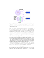
Figure 2.1: Overview of experiment components. (1) Laser diode and mount,
(2) optical isolator, (3) dielectric mirrors, (4) fibre coupling, (5) beam expansion telescope, (6) plate beam-splitter, (7) interferometer arm end mirror on a
translating stage, (8) CCD camera. Optical components undergoing testing are
inserted between the beam-splitter and one of the end mirrors.
Figure 2.2: Sharp GH04020A2GE laser diode pin configuration. The laser diode
package does not contain a monitoring photodiode, so the laser diode itself is
connected across pins 1 and 3.
11
Figure 2.3: ThorLabs LDM21 laser diode mount. Toggle switches can change
the polarities of the diode pin sockets labelled by LD, PD and G. ‘L’ refers to
the laser diode while ‘P’ refers to the photodiode. ‘A’ means ‘anode grounded’
while ‘C’ means ‘cathode grounded.’
2.2
Laser Diode Spectral Characteristics
The laser diode from Sharp is longitudinally multimode, with its emission spectrum consisting of closely spaced peaks over a range of about 1 nm and enveloped
by a gain profile (Fig. 2.4). We can estimate the coherence length according to
§3.6 of [8]
∆ντc ≈ 1
where ∆ν is the frequency linewidth and τc is the coherence time. From this,
and assuming a linewidth of 1 nm, the coherence length is less than 1 mm. This
sets a strict limit on the alignment of the optics, because if the optical path
difference (OPD) of the interfering beams exceeds this coherence length, we will
not observe clear interference fringes.
However, further analysis reveals that the question of laser diode coherence
requires a more sophisticated answer, because the width of the gain profile
enveloping the multiple emission peaks is not a good approximation for the
linewidth used in the previous calculation, which comes from considering the
broadening of a single mode line.
If we instead treat the spectrum more accurately as a series of regularly
spaced peaks in frequency with a gain profile that we will assume to be Gaussian, we arrive at different conclusions for laser diode coherence that are experimentally verified. To begin, the simplest case is to consider two such peaks
separated by a small ∆ω, with the left side peak at ω0 >> ∆ω (Fig. 2.5,
top). This is the well known phenomenon of beating between two frequency
12
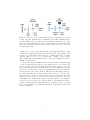
Figure 2.4: Sharp laser diode emission spectrum at room temperature and various power settings. There are multiple mode peaks in the spectrum, enveloped
by a gain profile.
components
cos(ω0 t) + cos[(ω0 + ∆ω)t] = 2cos[
∆ω
(2ω0 + ∆ω)
t]cos(
t)
2
2
with a slow beat frequency ∆ω enveloping a fast oscillation at (2ω0 + ∆ω)/2.
The beat frequency is ∆ω instead of ∆ω/2 because envelope maxima differ in
phase only by π. It is easy to see that our full treatment is simply an extension
of this analysis. For five equal amplitude frequency components (Fig. 2.5,
middle), the beat pattern becomes more complex but the underlying periodicity
remains unchanged. In the full treatment, we add a Gaussian envelope to these
five peaks, and again we observe the same underlying periodicity with a slight
change in the beat pattern (Fig. 2.5, bottom).
In this analysis, the individual spectrum peaks were taken to be infinitely
narrow, meaning that these individual modes have an infinite coherence length.
Consequently the beat patterns depicted (Fig. 2.5) also extend to infinity, and
this extension becomes truncated as we consider the broadening of the discrete
spectrum peaks, which reduces the coherence lengths of the individual emission
modes. Clearly, then, coherence length depends more on the linewidths of the
individual spectrum peaks than the shape of the overall gain profile, meaning
that the coherence length of our Sharp laser diode is orders of magnitude greater
than the 1 mm estimated at the start of this section. This bodes well for using
such a light source for interferometry.
13
Figure 2.5: Analysis of laser diode coherence in Mathematica. Functions composed of sums of cosines at the indicated frequencies are plotted to examine
their behaviours. For simplicity the phase of each cosine was set to zero, and
∆ω/ω ≈ 1/400. (top) Two equal amplitude spectrum peaks showing the classic beating phenomenon. (middle) Five equal amplitude peaks. (bottom) Five
peaks in a Gaussian envelope.
14
Looking at the behaviour of the laser emissions we are studying (Fig. 2.5), it
is also apparent that if two such beams undergo interference with one another,
the greatest fringe visibility is achieved when the envelope maxima overlap. As
the OPD between the two interfering beams is changed, this overlap will be
periodic at the beat frequency ∆ω, and likewise for the fringe visibility. This
periodicity of the fringe visibility is experimentally observed in §2.6.
The phenomenon of periodic fringe visibility suggests another solution to the
problem of multiple spurious reflections in a Fizeau interferometer described in
§1.3. Assuming that the internal reflections within each individual optical component interfere with low fringe visibility due to a non-ideal OPD, the separation
between the two objects can be adjusted to maximize interference fringe visibility between reflections from the surfaces of interest. However, experimental
measurements, described in §2.6, showed that the spurious internal reflections
produced fringes that were already highly visible, meaning that this proposed
solution would not work.
2.3
Dielectric Mirrors
Before I describe the remaining optics in greater detail, it is worth mentioning
the decision involved in the choice of mirrors for the experiment. Three dielectric
coated candidates were considered - ThorLabs E01, E02, and New Focus 5100.
From the theoretical reflectivity plots (Book 1: p. 110-112 of [9] and also
the online catalogs) the high reflectivity plateau shifts to higher wavelengths
as the angle of incidence goes to 0◦ . Since 405 nm is already at the short
wavelength end of the E02 coating range, the decision was made to acquire only
the ThorLabs E01 and the New Focus 5100 mirrors for testing.
The actual measurements of mirror reflectivities unearthed further complications due to non-uniformities across the active area of the power meter in the
lab (Fig. 2.6). This is a consequence of damage to the attenuation filter on the
power meter, and for comparison see Book 1: p. 146-149 of [9], where measurements were taken at low laser diode power with the attenuation filter removed.
Decisive measurements were taken after a good quality beam was obtained out
of a coupled fibre, and a large-area photodiode was substituted for the power
meter. The results, summarized in Book 1: p. 157 of [9], revealed reflectivities
that were virtually indistinguishable. However, the New Focus 5100 mirrors
seemed to perform marginally better, and coupled with the fact that its high
reflectivity plateau is centered around 405 nm rather than bordering on it, this
mirror was selected as the winner.
2.4
Remaining Optical Components
Following the optical path depicted in the experiment overview (Fig. 2.1), light
from the 405 nm laser diode is sent through an optical isolator to shield the
laser against back-reflections from optical components along the beam path. To
15
Figure 2.6: Scan across the power meter active area at constant laser diode
power revealed significant variations caused by damage to the attenuation filter.
Such non-uniformity makes it challenging to perform power measurements for
mirror reflectivity and other tests.
improve the laser diode beam shape, light is coupled into a single-mode optical
fibre. Beam quality is crucial for interferometry, because fluctuations in the
intensity profile of two interfering beams should come from phase differences
between the beams rather than distortions from the light source itself. Due
to the power meter problems described in §2.3, it was a challenge to carefully
determine the fibre coupling efficiency. The best current estimate, from the
careful measurements documented in Book 2: p. 58-60 of [9], is around 50%.
The beam emerging from the optical fibre goes through a 4x beam expansion
telescope, taking the beam diameter from about 2 mm to 8 mm, to provide
sufficient beam area for optics testing. The lenses in the telescope are chosen
to minimize spherical aberrations [10]. The incoming light is divided along
two paths by a plate beam-splitter to form the two interfering beams. The
plate-beam splitter has a coated front surface and a wedged back surface, which
avoids the internal reflection problems present in cube beam-splitters. It is also
more stable than pellicle beam-splitters, which are sensitive to vibrations and
inappropriate for use in an interferometer.
One end mirror in the interferometer, in the Twyman-Green configuration,
is mounted on a translating stage in order to allow for fine adjustments of the
OPD between the two interfering beams. Such adjustments are necessary to
obtain an OPD that maximizes the fringe visibility according to the analysis in
§2.2. The interfering beams are directed towards a CCD camera, which records
the interferogram for analysis.
16
2.5
CCD Camera
Shortly before the start of the summer, the lab acquired a pair of PixelFly QE
cameras from PCO. There are three important pieces of documentation for the
camera
• PixelFly Operating Instructions (2006 version directly from PCO [11] is
more in depth than the 2002 version from Cooke which is included on the
CD accompanying the camera)
• PCO Camware User’s Manual, which describes the features of the default
image processing software from PCO
• PixelFly Software Development Kit, which contains detailed instructions
about how to write code to interface with the camera hardware drivers
Camware, in particular, contains a useful ‘Camera Control’ window which
can display the CCD electronics temperature. The PixelFly camera does not
contain an active cooling system, and is designed to shut-down if the CCD
temperature exceeds 65◦ C (this is not in the manual, but is given in the online
FAQ’s for the PixelFly VGA - the less sensitive version of the QE). The camera
begins to warm up as soon as it is powered, even if it is not acquiring an image,
and typical temperatures when powered but dormant for extended periods of
time are 53◦ C for the unit with serial number 270 XD 13933, and 48◦ C for the
unit with serial number 270 XD 13934. Significant changes to these steady state
temperature levels might indicate the onset of camera hardware failure.
In addition to the software provided by PCO, the camera has also been made
to work with various programs written within the lab. For example, the interferogram analysis method described in Chapter 3 requires images to be saved
in a MATLAB file format, and this is done with an image processing program
written in Python. Additional notes about the PixelFly camera, including detailed instructions for its use in both interferometric optical testing and imaging
of trapped atoms, are included in Appendix A.
It is important to be careful not to damage the camera by exposing it to a
focused laser beam. As a safeguard, a negative lens has been placed in front of
the camera (Fig. 2.7) to gently expand any incident beam. Also, an attenuator
in the form of a neutral density filter is present to further protect the CCD
chip from overexposure. Finally, a movable positive lens in front of the camera
allows adjustments to the size of the beam at the image plane of the camera.
2.6
Early Experiments
In this section I will describe some of the earliest experimental work with the
Twyman-Green interferometer. This mainly involved observing interferograms
qualitatively for properties such as fringe visibility and distortion. A more
sophisticated and quantitative analysis method for extracting phase information
from these interferograms can be found in Chapter 3.
17
Figure 2.7: A C-mount to SM1 adapter is used to change the PixelFly camera
thread to that of the ThorLabs lens tubes. A neutral density filter and a negative
lens are attached to the camera body. A separate, movable positive lens can be
positioned to determine the beam diameter at the image plane of the camera.
One of the first measurements was to test whether fringe visibility behaves as
described in §2.2. In Book 1: p. 160 of [9] the recorded results show that fringe
visibility is indeed periodic, reaching consecutive maxima as the interferometer
end mirror was translated by 1.5 mm, which corresponds to an OPD of 3.0
mm. Some brief calculations outlined shortly thereafter on p. 185 gives an
estimate of the wavelength separation between modes as ∆λ ≈ 0.05 nm (the
general approach is to assume that the envelope period is the same as in the
two-frequency-beating case). From the Sharp laser diode output spectrum at
20 mW (Fig. 2.4, top) we can estimate that there are about 12 peaks over a
0.6 nm range (by counting peaks and measuring their range relative to the given
scale). This gives a mode separation of about 0.055 nm, which compares very
favourably to the previous computed value.
Experimental efforts also demonstrated qualitatively the predicted variations
in fringe visibility with OPD. For example, the fringe visibility changes depending on whether the interferometer arms are empty (Fig. 2.8). For a window
of thickness d and index of refraction n, the OPD introduced after each pass
is (n − 1)d, which can be much larger than a wavelength (take for instance, d
= 1 mm and n = 1.5). This means that using our Sharp laser diode as the
light source, the interferometer arm lengths must be adjusted with each new
test object in order to maximize fringe visibility.
Some of the objects that were tested include microscope slides, sapphire
windows, and thick vacuum windows (Fig. 2.9). In particular, see Book 2:
p. 15 and 37 of [9] for detailed specifications of the various sapphire windows
acquired from Meller Optics. The windows with part numbers A00E30471007
and SCD2889-02A were of a suitable size for the ThorLabs LMR05 lens mount,
and these were tested both in these early experiments and later ones involving
Fourier transform analysis. Further details of the early tests can be found in
Book 2 of [9].
Attempts were also made to produce interferograms using reflections from
the surfaces of the optical components under testing, in a configuration equiva-
18
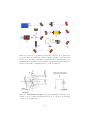
Figure 2.8: Comparison of fringe visibilities when a microscope slide is inserted
into part of the beam, corresponding to the left side of each interferogram. (left)
End mirror adjustments made to maximize the fringe visibility of the empty-arm
half of the interferogram, showing clear straight fringes. (right) Interferometer
arm length now adjusted to maximize the fringe visibility of the microscope
slide half of the interferogram.
Figure 2.9: Various methods for mounting optical components for testing in the
interferometer. (left) A microscope slide was taped to a mirror mount. (middle)
Sapphire windows of suitable size can be inserted in a ThorLabs LMR05 lens
mount. (right) A vacuum window in its flange is held in a large lens mount.
19
lent to that of a Fizeau interferometer. These are recorded in Book 2: p. 21-22,
27, 33-36 and 39 of [9]. While the aim was to observe interference between one
reflected beam from each of the two optical components, a test object and a
reference object, experimentally the reflections from the two surfaces of each
individual object already produced strong interference fringes. This problem,
which was anticipated in §1.3, made it impossible to use this interferometer
configuration to extract any sort of information about the wavefront distortions
due to the test object.
While a working Fizeau interferometer is crucial to measurements of vacuum window distortions under a pressure differential, the decision was made
to continue onwards to devising interferogram analysis methods using the more
successful Twyman-Green configuration, with the knowledge that such methods
would also be applicable to the Fizeau interferometer as well once the experimental obstacles of this configuration are overcome.
20
Chapter 3
Interferogram Analysis
3.1
Survey of Popular Approaches
There are a number of approaches to the problem of interferogram analysis.
One is to fit the obtained interferogram to Zernike polynomials, which are a set
of functions that describe the interferogram appearance resulting from various
types of aberrations such as tilt, defocusing and astigmatism. More in-depth
descriptions of these polynomials can be found on p. 24-29 of [7] and in Chapter
13 of [6]. The coefficients obtained in this fit are an indication of the amount of
aberration of each type present in the optical component under test, and this can
then be transformed into a measure of phase distortion. However, complicated
fringe finding algorithms are required to define the locations of fringe centers
in an interferogram order to map the distortions in the fringe pattern. The
supplementary disk that comes with [6] contains a program which can generate
interferograms according to user-specified Zernike polynomial coefficients. This
is also installed in the ‘:\OpticsTesting\Interferogram’ directory on the disk
included with [9], and it is useful for getting a sense of how various distortions
affect the appearance of interferograms. Unfortunately it cannot do the reverse.
Another approach is known as phase shifting interferometry (PSI). It is explained in detail on p. 32-42 of [7] and Chapter 14 of [6]. Ideally it would
be possible to compare two interferograms - one with the optical test component in place and one with empty interferometer arms - and extract the phase
distortion information from the changes in intensity at each point of the two
corresponding interferograms. Practically, however, this does not work, because
of the unavoidable non-uniformities in the source beam of light. PSI solves
this problem by shifting the phase of one of the two interfering beams by known
amounts using, for example, piezoelectric crystals. A minimum of three such interferograms are taken, and these can be analyzed to extract information about
the phase. This proposal is obviously complicated by the need for piezoelectric
crystals to generate well defined shifts. A simpler method exists for extracting
the phase profile of light passing through the optical testing component using
21
only a single interferogram. This is known as the Fourier transform method of
interferogram analysis.
3.2
Fourier Transform Method
The Fourier transform method of interferogram analysis is a remarkable method
of extracting phase information that does not involve either fringe finding or
phase shifting. The basic theory presented here closely imitates the approach
of the original paper [13]. The method is also explained on p. 43 of [7] and in
§14.14.5 of [6].
A 2D interferogram consisting of phase distortions on top of straight fringes
in the horizontal direction can be described by
g(x, y) = a(x, y) + b(x, y)cos[ω0 x + φ(x, y)]
(3.1)
where a(x, y) represents the background and b(x, y) takes into account nonuniformities in the interfering beams. The spatial frequency of the fringes is
determined by ω0 while φ(x, y) is the term corresponding to the added phase
distortions. Equation 3.1 can be rewritten as
g(x, y) = a(x, y) + c(x, y)exp(iω0 x) + c∗ (x, y)exp(−iω0 x)
(3.2)
1
b(x, y)exp[iφ(x, y)]
2
If we take the Fourier transform in x of Equation 3.2 we get
c(x, y) =
G(ω, y) = A(ω, y) + C(ω − ω0 , y) + C ∗ (ω + ω0 , y)
(3.3)
where the capitalized letters denote the corresponding Fourier transformed functions. Now comes a key assumption: suppose that spatial variations of a(x, y),
b(x, y) and φ(x, y) are slow compared to the spatial frequency ω0 of the underlying fringes. This means that the frequency-space widths of A(ω, y) and C(ω, y)
are small compared to ω0 , and we see that the plot of Equation 3.3 would consist
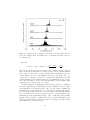
of three separate peaks (Fig. 3.1).
If we then apply a bandpass filter to isolate C(ω − ω0 , y), followed by a
shift of −ω0 , we recover C(ω, y), which can be Fourier transformed back to give
c(x, y). If we now apply the logarithm function
1
ln[c(x, y)] = ln[ b(x, y)] + iφ(x, y)
2
which suggests how the phase information can be extracted
φ(x, y) = Im{ln[c(x, y)]}
(3.4)
Clearly, this outlined method rests crucially on the assumption that spatial
variations of a(x, y), b(x, y) and φ(x, y) are slow compared to ω0 . As a result,
this method of analysis is inappropriate for interferograms with high levels of
22
Figure 3.1: Three separate peaks in the Fourier transformed spectrum of an
interferogram. The two side peaks are symmetrical about the origin, and contain
information about the phase distortions described by the interferogram.
distortions, but for our tests of high quality optical components with only small
levels of distortions expected, the Fourier transform method of interferogram
analysis is a straightforward and accurate way of obtaining the phase profile of
light passing through our test object.
3.3
Implementation in MATLAB
A suite of functions were written in MATLAB to analyze interferograms according to the method described in §3.2. These can be found on the disk included
with [9], in the ‘:\MATLAB Code’ directory. The following summarizes the
contents of the files
• analysis.m: main analysis script. Requires an image array named ‘image1’ to be loaded into the MATLAB workspace
• image display.m: displays a scaled version of image array with a specified colour map
• array crop.m: crops an image array in a rectangular window based on
input parameters
• image 1Dft.m: performs a Fourier transform in the x direction on a single specified row in an array. User can choose to display only a particular
interval of the entire Fourier spectrum
• image 2Dft.m: performs a Fourier transform in the y direction on the
entire 2D array
• image getphase.m: takes a Fourier transformed interferogram image array and performs the operations specified in §3.2 to obtain phase function.
Requires the user to define the center and width of the side peak.
23
Figure 3.2: Fourier transform of an interferogram (using ‘image 2Dft.m’) showing the three characteristic peaks corresponding to the three vertical white
stripes. Note that the spectrum has been shifted to bring the zeroth-order
peak to the center of the image, so the horizontal scale has been shifted such
that 300 corresponds to 0.
• phase unwrap.m: performs 2D phase unwrapping on a given array
• compute rms.m: compute the standard deviation of data points in a
2D image array and outputs to the command line. This calculates the
root-mean-square phase distortions in the obtained phase profile.
The main analysis script ‘analysis.m’ performs the required tasks in several
steps by calling the other defined functions. Before it is executed, an image
array with the name ‘image1’ must be loaded into the MATLAB workspace, for
example by opening one of the MATLAB image data files saved by PyCamera.
The user may specify additional cropping dimensions for this image to remove
noisy edge areas. The image is Fourier transformed (Fig. 3.2), and by looking at
plots of the spectrum along individual rows of the image (using ‘image 1Dft.m’),
the user can isolate the side peak and define its center and width.
With the side peak defined, the analysis script proceeds to calculate the
phase profile φ(x, y). Due to the properties of the Fourier transform, the calculated phase will be restricted to the range from −π to +π. However, the actual
phase has no such restriction, and thus may differ from the calculated phase by
multiples of 2π. This is the phenomenon of phase wrapping (Fig. 3.3). To determine the actual phase profile, the wrapped phase must be unwrapped. Along
a single axis this is simple and the method is described in [13]. In the current
MATLAB implementation this has been extended to work in two dimensions
simply by unwrapping the first column, then unwrapping each row to obtain
the full 2D unwrapped phase function. Once the unwrapped phase function
24
Figure 3.3: Plot of the wrapped phase function calculated from the interferogram. The scale on the right goes from −π to +π. Note the distinct phase
jumps marked by sharp transitions between white and black. Marked regions
correspond to noisy points along the first column that will cause errors to occur
in phase unwrapping.
has been computed, useful measures such as the root-mean-square (rms) phase
distortion can be calculated
1q N
∆φrms =
Σj=1 (φj − φ̄)2
N
Here φj is the phase at each point while φ̄ is the average phase across the entire
region of interest and N is the total number of sample points.
3.4
Discussion of Results
The unwrapping algorithm described in §3.3 will produce errors in the unwrapped phase function when the original wrapped phase is too noisy (Fig.
3.4), for example when there are actual phase differences of more than π between adjacent sample points. The current solution is to simply restrict the
region of interest to a smaller, less noisy area. Other highly complicated phase
unwrapping algorithms exist to properly unwrap phase functions in the presence
of such noise [14].
After decreasing the region of interest and repeating the analysis from the
beginning, the unwrapped phase profile becomes a smooth function (Fig. 3.5
- 3.8). The sample that has been tested in this case is a high quality sapphire
window (SCD2889-02A), and the calculated ∆φrms is 0.27 waves. Note that the
underlying phase distortions in the empty arm interferometer due to imperfections in the optics gives a base ∆φrms of about 0.15 waves. For comparison, a
25
Figure 3.4: Example of errors in phase unwrapping. The unwrapped phase
function contains several distinct discontinuities in the vertical direction that
are the result of excessive noise at points along the first column of the wrapped
phase (Fig. 3.3).
Figure 3.5: Plot of wrapped phase function (Fig. 3.3) in a smaller region of
interest. The noisy points along the first column of the previous plot are no
longer present.
26
Figure 3.6: Successful unwrapping of the previous phase function (Fig. 3.5),
resulting in a smoothly varying phase profile across the entire region of interest.
The 600 pixel width corresponds to about 2-3 mm of transverse beam area
microscope slide and a thick vacuum window have ∆φrms equal to 0.91 and 0.18
waves respectively. The region of interest in all these cases is a square of 600
pixels in length, which corresponds to approximately 2-3 mm of the transverse
beam area. A full record of these tests can be found in Book 2: p. 89-101 of [9].
It is interesting that the thick vacuum window shows less evidence of wavefront distortions compared to the expensive high quality sapphire window. On
the one hand, this could be due to the fact that the sapphire window is extremely thin, making it much more difficult to produce low distortion surfaces.
On the other hand, the distortion measurements in this report were performed
using a collimated beam at normal incidence on the window. As mentioned
in §1.1, greater distortions due to spherical aberrations in the thick vacuum
window would have been observed for an incident beam with a larger N A, and
these distortions will certainly be relevant to the actual high resolution imaging
system. Two other pieces were also tested - another sapphire window of lower
quality and a crude piece of transparent plastic - but both plots of the wrapped
phase showed significantly more distortions compared to the other test objects,
and were too noisy to be unwrapped in the given region of interest.
3.5
Possible Errors in Interferogram Analysis
There are two obvious possible errors that can occur in using the interferogram
analysis algorithm described in §3.3. First of all, Equation 3.1 assumes that
the underlying straight fringes are in the x direction. If the interferometer is
misaligned and the fringes are tilted, it is clear that the calculated phase function
27
Figure 3.7: Plot of data points along the center row (300) in the wrapped phase
function (Fig. 3.5). The horizontal scale is the pixel number while the vertical
scale is the phase. A width of 600 pixels corresponds to approximately 2-3 mm
in the transverse beam area. A clear phase jump between π and −π is observed
between pixels 500 and 600.
Figure 3.8: Plot of data points along the center row (300) in the unwrapped
phase function (Fig. 3.6). The horizontal scale is the pixel number while the
vertical scale is the phase. A width of 600 pixels corresponds to approximately
2-3 mm in the transverse beam area.
28
Figure 3.9: The effect of errors in defining the side peak is demonstrated in
comparison to the original wrapped phase function (Fig. 3.5). Note that this
wrapped phase function shows a significant gradient in the x direction.
will have a large gradient in the y direction. It seemed to be sufficient during
this project to simply make sure visually that the fringes are vertically aligned.
Alternately one could include a simple MATLAB array rotation function in the
analysis script to rotate the fringes until they are completely vertical.
The other source of error is more subtle but can be easily corrected. The
analysis algorithm in §3.3 requires the user to define the center of the side peak
by examining plots of Fourier transforms along rows in the interferogram. It is
possible that a mistake will occur, and the center of the side peak will be defined
at ω1 = ω0 + ωe instead of ω0 , with ωe being the frequency error. Following the
steps described in §3.2, when the side peak is shifted back it will be displaced
by ωe from the origin, and upon Fourier transforming back to recover c(x, y) the
result is instead c1 (x, y) = exp(iωe x)c(x, y). The extra factor exp(iωe x) comes
from the relationship between Fourier transformed pairs, where a translation of
one leads to an imaginary exponential factor in the other. Now, if we substitute
the original expression for c(x, y) we have
c1 (x, y) =
1
b(x, y)exp[iφ1 (x, y)]
2
where φ1 (x, y) = φ(x, y) + ωe x. This clearly implies that an error in defining
the side peak will result in a large phase gradient in the x direction.
29
Chapter 4
Future Directions
There are still many areas in which efforts can be made to improve the current
interferometric optical testing method, bringing the overall experiment closer to
its goal of high resolution imaging of individual sites in an optical lattice. These
are elaborated upon below in two sections: experiment design and analysis
methods. I do not expect all these suggestions to be acted upon, because on the
one hand they might not be intelligent ideas, and on the other hand at some
point the interferometric optical testing experiment might work sufficiently well
that further improvements would not contribute significantly towards the overall
high resolution imaging effort. The points in each section are organized, from
my perspective, in order of priority.
Improvements to Experiment Design
• A possibly significant source of noise in the current experiment is diffraction from dust particles on various optics. These produce circular fringe
patterns which distort the interferogram (see, for example, Fig. 2.8) and
increase the calculated root-mean-square phase distortion in the MATLAB
analysis. Currently the most significant source of these spurious fringes is
a dirty neutral density filter placed in front of the CCD camera to attenuate the laser beam. It has been carefully cleaned but it seems that some
of the damage is permanent. Fringes due to scattering from point sources
on other optical surfaces can be cleaned up by spatial filtering with a lens
and pin-hole combination in front of the camera
• Improved beam quality will allow phase distortion calculations to be done
on a larger interferogram area. Currently the interferogram has its noisy
edges cropped, because phase unwrapping would not succeed otherwise.
This, unfortunately, limits the cross-sectional area of the optical component that can be analyzed for wavefront distortions. The main improvement to beam quality should come from a better alignment of the beam
expansion telescope
30
• Different geometries, such as the Mach-Zehnder configuration, can be attempted. Both of the current geometries, the Twyman-Green and the
Fizeau, cannot produce a beam that traverses exactly the same optical
path as would be the case for imaging in an actual lattice - namely, a
single transmission through all optical components in the imaging system
to the camera. The Mach-Zehnder is the only common interferometer
configuration that can test distortions due to single transmission through
an optical component. However, it is a challenge to align, especially given
the phenomenon of periodic fringe visibility observed for our light source
• Along a similar line of thought, to test for distortions in a set-up that
mimics the actual optical lattice imaging system as closely as possible,
it might make sense to focus the beam down using a large N A lens and
then pass the beam through an optical window shortly after the focus.
Of course the lens will introduce additional spherical aberrations to the
beam, but this will be present in both of the interfering beams, while
the final interferogram will only capture differences between them. Also,
approaches for testing components other than flat windows are offered in
[6] and [7]
• Using a single mode laser source can avoid the issues caused by periodic
fringe visibility, and possibly open up new possibilities for interferometer
configurations. However, narrow linewidth, long coherence-length light
sources are typically not used for interferometric optical testing because
they will introduce more spurious fringes from internal reflections within
various optical components
• A Geller MRS-5 optical target consisting of high density bar and square
patterns was acquired during the course of the summer for testing of imaging system resolution. However, the project did not proceed that far, but
the components are in place to test the change in pattern contrast when
illuminated by light which then passes through various optics such as vacuum windows and lenses. The PixelFly camera can be used to capture
an image of the optical target pattern, and this can then be analyzed in
MATLAB in much the same way that the interferograms were studied
Improvements to Analysis Methods
• Currently, the calculations for root-mean-square wavefront distortions introduced by the optical components under testing do not subtract the
underlying phase variations of the empty arm interferometer, which is on
the order of λ/10. It would be a simple extension of the current analysis
algorithm to subtract the two unwrapped phase functions, one being that
of the test object and the other corresponding to the empty arm interferometer, and determine whether this gives a more accurate, reduced value
for root-mean-square wavefront distortions
31
• More sophisticated analysis techniques such as fitting the interferogram
to Zernike polynomials might give more information about the test object. For example, a program called AtmosFringe can fit the interferogram to determine aberration coefficients, and then compute useful quantities such as the point spread function (PSF) and the modulation transfer function (MTF) of the optical system under testing. A demo version
which can only analyze several example interferograms is installed in the
‘:\OpticsTesting\AtmosFringe’ directory on the disk included with [9]. A
more limited freeware program called FringeXP has also been installed in
the ‘:\OpticsTesting\FringeXP’ directory. It would be nice to try analyzing the captured interferograms using this program and compare the
results with the Fourier transform analysis in MATLAB. Finally, a powerful, but of course expensive, program called IntelliWave exists but I do
not know very much about it beyond its name
• It would be nice to implement a more sophisticated phase unwrapping
algorithm that is less sensitive to noise. However this would likely be
time consuming, and efforts might be better spent on improving the beam
quality to reduce phase unwrapping problems, as described above. For interferograms showing significant wavefront distortions, a visual inspection
of the wrapped phase function might be sufficient
32
Appendix A
PixelFly Camera Notes
In this Appendix I will provide instructions for how the PixelFly camera is to
be used in the lab. The camera has been programmed and tested for use in
both interferometric optical testing and imaging of trapped atoms.
A.1
Software Installation Issues
A number of difficulties were encountered with software installation at the start
of the summer. The lab’s main image processing program is written in Python,
using a specific version called the Enthought Python Distribution (EPD) which
includes a large collection of scientific computing libraries. Many of the library
references included in the program code turned out to be obsolete, with endless
errors arising when the program was executed with the newest version of the
EPD. The implemented solution was to install exactly the same version of the
EPD and its various associated libraries as was used when programming work
first began back in 2006. These install files can be found on the disk included
with [9], in the directory ‘:\PythonInstall’.
Another issue that came up was a ‘WindowsError,’ encountered when Python
attempted to load the DLL file written in C++ to interface with the camera
driver DLL. This can be resolved by installing Microsoft Visual Studio 2005 on
the system. If the error persists, it might also be necessary to recompile the
DLL file on the local computer.
A.2
Hardware Triggering
The camera can be triggered either by code in the software or by the rising
edge of a 5V pulse from an external signal generator. Camera signal timing
diagrams and further details about external triggering are given on p. 21-24
of [11]. The camera interacts with the external world via an unusual 26 pin
HD-DSUB port on the PCI controller card. A cable converting this port to a
single BNC connector for external hardware triggering was provided by PCO.
33
Figure A.1: Conversion from 26 pin HD-DSUB to four BNC connectors: (input)
external hardware triggering, (output) camera busy, CCD exposure, and image
buffer readout.
In addition, a pair of conversion boxes, one for each camera, were constructed
(Fig. A.1) to allow access to three additional output signals from the camera
which indicate the status of various internal processes.
A.3
Summary of Camera Programs
The programs described in this section, with the exception of CamWare (which
is installed as a Windows program), can be found on the disk included with [9],
in the directory ‘:\PixelFly\dev’. Note that because all the programs require
the same camera driver file ‘Pccam.dll’, only one can be running at a given time.
CamWare: included with the software disk from PCO. Gives easy access to
camera functions and contains the useful temperature monitoring window described in §2.5. Its drawbacks include being able to specify exposure time only
to a precision of 1 ms, and the lack of automated image analysis capabilities
such as Gaussian fitting that are vital to experimental work in the lab.
Demo Project: a sample C++ project supplied by PCO for controlling the
camera. From this project, and specifically ‘cam class.cpp’, I learned everything
about writing a DLL file in C++ to interact with the camera driver (Pccam.dll).
The Demo Project has a video mode (‘Cont. Pic1’ under the ‘Control’ menu)
which is useful for experiment alignment purposes. The exposure time can be
set to a precision of 1 µs by changing the value of the ‘iExp video’ variable
defined under ‘CpcCam::CpcCam(int board)’. This variable is an integer which
34
sets in microseconds the exposure time of each video frame.
PFDriver: this is a test-bed I wrote for accessing functions from the PixeFly camera drivers. Functions for one image acquisition cycle are called in
sequence with diagnostic text messages output to the command line. While
no image readout functionality has been implemented, the code does include
a timing algorithm to determine how long it takes to execute a block of code
between the lines ‘test.startTimer()’ and ‘test.stopTimer()’. This allows the
user to measure actual image readout times, which combine both the hardware
readout time given on p. 22 of [11] and the execution time of the code. Further
details can be found by referring to Book 1: p. 173-174 of [9]
PyCamera: a versatile image processing tool written in Python by Gaël Varoquaux and updated by Marcius Extavour. I learned Python by reading [12],
which is available online through the University of Toronto Libraries. The main
disadvantage of Python its inefficiency - tasks that can be performed effortlessly
in C++ cause noticeable delays in Python. On the other hand, because it is such
a high-level language, it is excellent for programming graphical user interfaces.
Those who first encounter PyCamera might be confused by various snippets of
code. The program uses a library called TraitsUI, which allows the programmer
to focus on designing attributes and methods of each object, while TraitsUI
automatically generates the appropriate user interface. Also, references to a
‘kinetics mode’ correspond to a Pixis camera feature that the PixelFly does
not have. See Appendix A.5 for more details about this. Important parts of
PyCamera are as follows
• pycamera.py: the core of the PyCamera program. This file is executed
to run PyCamera. An alternate ‘pycamera fast.py’ is a stripped down
version of ‘pycamera.py’ with no analysis capabilities. This decreases the
time it takes to go through an image acquisition sequence, although the
program is still limited to about two or three frames per second
• experiment.py: in this file, the line ‘from * import * as Camera’ determines which camera class the program will import. The options are
the PixelFly or Pixis cameras, or a ‘Mock Camera’ which is a simulated
camera that always displays an image of an idealized cold atom cloud
• lib pf.dll: found in the subdirectory ‘\C interface\PixelFly’ and wraps
functions from the camera driver DLL in a way that can be accessed from
Python. This interface was necessitated mainly by the fact that I could
not figure out how to deal with the data type ‘HANDLE’ from the camera
drivers directly in Python
• pixelfly interface.py: imports the wrapped functions from ‘lib pf.dll’
and defines Python functions for them
• pixelfly camera.py: contains the definition of the camera object, which
is a set of attributes and methods, calling on the functions defined in ‘pix35
elfly interface.py’. Other program elements reference this camera object,
so attribute and method names were kept as consistent as possible with
the corresponding Pixis camera object definition in ‘pixis camera.py’
My contribution to PyCamera consists of the last three items, which enable
the program to control the new PixelFly cameras acquired by the lab. The
‘lib pf.dll’ file was built in a C++ project located in the ‘:\PixelFly\dev\lib pf’
directory on the disk included with [9]. The compiled DLL file is stored in
the PyCamera program folder, with the path ‘\C interface\PixelFly’. Both
‘pixelfly interface.py’ and ‘pixelfly camera.py’ are stored in the root PyCamera
folder ‘:\PixelFly\dev\PyCamera’.
A.4
Interferometric Optical Testing
As mentioned in Appendix A.3, for initial interferometer alignment it is best to
use the Demo Project from PCO, because it is written in C++ and can achieve
fast frame rates, whereas PyCamera can only manage two or three frames per
second even when analysis algorithms are disabled. Once it is clear that the
camera is capturing an interferogram of sufficient quality, the user can switch
to image acquisition using PyCamera (Fig. A.2).
The camera should be set to single exposure with software triggering. Also,
in the ‘Acquisition’ tab the ‘Save images’ box should be checked. This will
bring up a window for the user to specify the folder and file name under which
the images will be saved. PyCamera will append both a four-digit index and
the MATLAB extension ‘.mat’ to the specified path. At this point, activating
the ‘Toggle’ button will produce a set of MATLAB files corresponding to each
image acquired. Each file, when opened, will contain at least two image arrays
‘image1’ and ‘image2’. The second of these is simply a blank image in the
single exposure mode of operation, so only ‘image1’ needs be imported into
the MATLAB workspace. Analysis of this imported interferogram image then
proceeds as outlined in §3.3.
A.5
Imaging of Trapped Atoms
The main difference between using the PixelFly camera to image trapped atoms
and using it to capture interferograms is the fact that absorption imaging of
atoms requires a more sophisticated acquisition sequence. Absorption imaging
to obtain the optical density of atoms in a trap involves taking two images in
quick succession. In the first image, a probe laser beam illuminates the atoms,
which absorb part of the beam. The second image is simply a reference image
of the laser beam without any atoms present. If the intensity distributions
captured by the camera are I and I0 respectively, then the optical density (OD)
is defined as
I
OD = −ln( )
(A.1)
I0
36
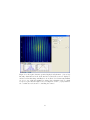
Figure A.2: An acquired interferogram is displayed in PyCamera. (bottom left)
Intensity distributions in the horizontal and vertical directions are displayed,
and it is evident that fringe visibility here is excellent. Periodic intensity minima
are close to zero while the maxima are arranged in a Gaussian envelope, which
is expected given that the light source is a single-mode fibre. (right) ‘Camera’
tab contains user selections for controlling the camera.
37
The reason the images must be taken in quick succession is to reduce unwanted
noise effects. For example, there are spurious fringes resulting from internal
reflections within various optical components. If the time between exposures
is short enough that the fringes do not shift significantly (this depends on the
frequency of mechanical vibrations in the system and should be less than 1 ms,
which is far shorter than typical CCD camera readout times), then the computation for OD in Equation A.1 will cancel out any intensity variations due to
these fringes.
The previous camera model used to image atoms in this way was the Pixis.
It had a ‘kinetics mode’ to get around the limitation of CCD readout time
and enable fast double exposures. The CCD chip would be divided in the
vertical direction into regions of equal height, and only one of these regions
would actively acquire images. The others act as image buffers, and after one
image is taken, the charges are quickly shifted to a buffer region to allow a
second exposure to occur. This ‘kinetics mode’ is fast because shifting charges
between areas of a single CCD chip can be done much more quickly than charge
readout from the entire chip into a memory buffer.
The PixelFly camera does things a little differently. It has an interline CCD
architecture, meaning that for every line of active imaging pixels, there is a
corresponding line of masked pixels whose sole task is to be a temporary image
buffer. The image readout process occurs via first shifting charges from the
active to the masked pixels, and then reading out to an actual memory buffer.
As with the Pixis camera, charge shifting can occur very quickly while charge
readout to a memory buffer consumes most of the image acquisition time. To
take two images in quick succession, the first exposure occurs, and while the
charges from this first image are in the buffer pixels being read out, the active
pixels are exposed again for the second image. A key limitation is the fact
that the exposure time of the second image cannot be independently specified it must be equal to the time it takes to read out the first image. Thus, actual
exposure times must be determined externally through the timing of probe laser
beam pulses. Further description of this special mode of operation can be found
by referring to p. 23 of [11].
In the PyCamera interface (Fig. A.2), setting up the camera to take two
shots with either type of trigger signal and ‘Dual Trigger’ = 0 will enable this fast
double exposure mode of image acquisition. With hardware triggering and ‘Dual
Trigger’ = 1, the PixelFly camera can also take two slow single exposures defined
by two external trigger pulses. The purpose of this slower double exposure mode
of operation is to enable absorption imaging tests of a magneto-optical trap, in
which atom dissipation times are long enough that no real advantage is gained
by taking fast double exposures. Performing two single exposures, on the other
hand, allows much greater control over the timing of each individual image.
38
Bibliography
[1]
M. Born & E. Wolf. Principles of Optics, 7th Edition. Cambridge University Press, 1999
[2]
Y. R. P. Sortais et al. Phys. Rev. A. 75, 013406 (2007)
[3]
A. Mazouchi. Feasibility of Single Atom Imaging in an Optical Lattice.
M.Sc. Thesis, University of Toronto, 2007
[4]
M. Greiner & S. Fölling. Q&A: Optical Lattices. Nature, 453, 736 (2008)
[5]
K. D. Nelson et al. Nature Phys. 3, 556 (2004)
[6]
D. Malacara. Optical Shop Testing, 3rd Edition. Wiley, 2007
[7]
E. P. Goodwin & J. C. Wyant. Field Guide to Interferometric Optical
Testing. SPIE Press, 2006
[8]
G. Fowles. Introduction to Modern Optics, 2nd Edition. Holt, Rinehart
and Winston, 1975
[9]
T. Wang. Lab Notes (2 Volumes). Summer 2008
[10]
Aberration Balancing. Melles Griot Catalog X §1.27-1.28, 2005
[11]
PixelFly QE Operating Instructions. PCO, 2006
[12]
M. E. Hetland. Beginning Python. Apress, 2005
[13]
M. Takeda et al. J. Opt. Soc. Am. 72, 1 (1982)
[14]
D. C. Ghiglia et al. Two-Dimensional Phase Unwrapping. Wiley, 1998
39