1
Part I: PCM-051/phyCORE-AM335x System on Module
phyCORE-AM335x
3.7 System Memory
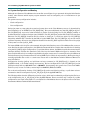
The phyCORE-AM335x provides four types of on-board memory:
•
DDR3 SDRAM
•
NAND Flash
•
SPI Flash
•
I2C-EEPROM
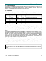
These following sections of this chapter detail each memory type used on the phyCORE-AM335x.
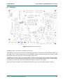
3.7.1 DDR3-SDRAM (U7, U9)
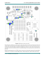
The RAM memory of the phyCORE-AM335x is comprised of two 8-bit wide DDR3-SDRAM chips at U7 and U9.
The effective bus is 16-bits wide. The chips are connected to the dedicated DDR interface called the Extended
Memory Interface (EMIF) of the AM335x processor.
The DDR3-SDRAM memory is accessed via the EMIF0 port starting at 0x8000 0000.
Typically the DDR3-SDRAM initialization is performed by a boot loader or operating system following a
power-on reset and must not be changed at a later point by any application code. When writing custom code
independent of an operating system or boot loader, SDRAM must be initialized through the appropriate SDRAM
configuration registers on the AM335x controller. Refer to the AM335x Technical Reference Manual about
accessing and configuring these registers.
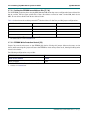
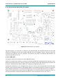
3.7.2 NAND Flash Memory (U10)
The use of NAND flash as non-volatile memory on the phyCORE-AM335x provides an easily reprogrammable
means of code storage.
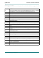
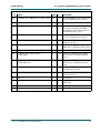
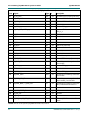
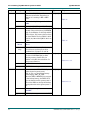
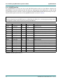
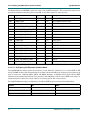
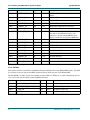
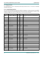
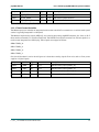
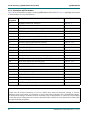
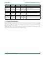
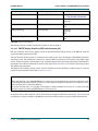
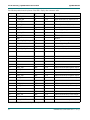
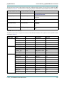
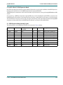
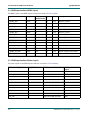
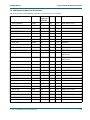
The NAND Flash memory is connected to the AM335x GPMC interface with a bus-width of 8-bits on its CS0
chip-select signal. The full GPMC interface is available on the phyCORE connectors. See the AM335x datasheet
for the pin-multiplexing options. The locations of the subset of the GPMC interface used for the NAND flash is
shown in Table 12.
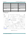
Signal
SOM pin
GPIO ExpanType
sion Board Pin
SL
Description
X_GPMC_AD0
X1A23
3A
IO
3.3 V
Address / Data 0
X_GPMC_AD1
X1A16
2A
IO
3.3 V
Address / Data 1
X_GPMC_AD2
X1A24
5A
IO
3.3 V
Address / Data 2
X_GPMC_AD3
X1A28
6A
IO
3.3 V
Address / Data 3
X_GPMC_AD4
X1A25
8A
IO
3.3 V
Address / Data 4
X_GPMC_AD5
X1A26
9A
IO
3.3 V
Address / Data 5
X_GPMC_AD6
X1A29
11A
IO
3.3 V
Address / Data 6
X_GPMC_AD7
X1A30
12A
IO
3.3 V
Address / Data 7
X_GPMC_ADVn_ALE
X1A33
14A
IO
3.3 V
Address Latch Enable
X_GPMC_BE0n_CLE
X1A34
15A
IO
3.3 V
Byte 0 Enable
Table 12: NAND GPMC Signal Map
37
© PHYTEC Messtechnik GmbH 2012 L-771e_1