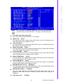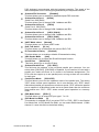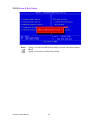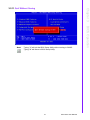
1
User Manual PCA-6743 DM&P Vortex86DX-800MHz SOC, ISA Half-size SBC, TTL, 10/100 Ethernet, CFC, On board memory Copyright The documentation and the software included with this product are copyrighted 2010 by Advantech Co., Ltd. All rights are reserved. Advantech Co., Ltd. reserves the right to make improvements in the products described in this manual at any time without notice. No part of this manual may be reproduced, copied, translated or transmitted in any form or by any means without the prior written permission of Advantech Co., Ltd. Information provided in this manual is intended to be accurate and reliable. However, Advantech Co., Ltd. assumes no responsibility for its use, nor for any infringements of the rights of third parties, which may result from its use. Acknowledgements Award is a trademark of Award Software International, Inc. DMP is a trademark of DMP Electronics Inc. IBM, PC/AT, PS/2 and VGA are trademarks of International Business Machines Corporation. Intel and Pentium are trademarks of Intel Corporation. Microsoft Windows® is a registered trademark of Microsoft Corp. RTL is a trademark of Realtek Semi-Conductor Co., Ltd. ESS is a trademark of ESS Technology, Inc. UMC is a trademark of United Microelectronics Corporation. SMI is a trademark of Silicon Motion, Inc. Creative is a trademark of Creative Technology LTD. CHRONTEL is a trademark of Chrontel Inc. All other product names or trademarks are properties of their respective owners. Part No. 2002674302 Edition 3 March 2013 PCA-6743 User Manual ii Product Warranty (2 years) Advantech warrants to you, the original purchaser, that each of its products will be free from defects in materials and workmanship for two years from the date of purchase. This warranty does not apply to any products which have been repaired or altered by persons other than repair personnel authorized by Advantech, or which have been subject to misuse, abuse, accident or improper installation. Advantech assumes no liability under the terms of this warranty as a consequence of such events. Because of Advantech’s high quality-control standards and rigorous testing, most of our customers never need to use our repair service. If an Advantech product is defective, it will be repaired or replaced at no charge during the warranty period. For outof-warranty repairs, you will be billed according to the cost of replacement materials, service time and freight. Please consult your dealer for more details. If you think you have a defective product, follow these steps: 1. Collect all the information about the problem encountered. (For example, CPU speed, Advantech products used, other hardware and software used, etc.) Note anything abnormal and list any onscreen messages you get when the problem occurs. 2. Call your dealer and describe the problem. Please have your manual, product, and any helpful information readily available. 3. If your product is diagnosed as defective, obtain an RMA (return merchandise authorization) number from your dealer. This allows us to process your return more quickly. 4. Carefully pack the defective product, a fully-completed Repair and Replacement Order Card and a photocopy proof of purchase date (such as your sales receipt) in a shippable container. A product returned without proof of the purchase date is not eligible for warranty service. 5. Write the RMA number visibly on the outside of the package and ship it prepaid to your dealer. Declaration of Conformity FCC Class A Note: This equipment has been tested and found to comply with the limits for a Class A digital device, pursuant to part 15 of the FCC Rules. These limits are designed to provide reasonable protection against harmful interference when the equipment is operated in a commercial environment. This equipment generates, uses, and can radiate radio frequency energy and, if not installed and used in accordance with the instruction manual, may cause harmful interference to radio communications. Operation of this equipment in a residential area is likely to cause harmful interference in which case the user will be required to correct the interference at his own expense. Caution! There is a danger of a new battery exploding if it is incorrectly installed. Do not attempt to recharge, force open, or heat the battery. Replace the battery only with the same or equivalent type recommended by the manufacturer. Discard used batteries according to the manufacturer's instructions. iii PCA-6743 User Manual Technical Support and Assistance 1. 2. Visit the Advantech web site at www.advantech.com/support where you can find the latest information about the product. Contact your distributor, sales representative, or Advantech's customer service center for technical support if you need additional assistance. Please have the following information ready before you call: – Product name and serial number – Description of your peripheral attachments – Description of your software (operating system, version, application software, etc.) – A complete description of the problem – The exact wording of any error messages Packing List Before setting up the system, check that the items listed below are included and in good condition. 1 PCA-6743 Series Half-size CPU Card 1 Startup manual 1 Utility CD 1 mini jumper pack Cables Part NumberDescription 1700060202 Y cable for PS/2 Keyboard, PS/2 Mouse 1700014398 4-port USB cable kit (2.0 mm pitch) 1701260305 COM2 (2.54 mm) + LPT (2.54 mm) cable 1700008762 Dual-COM port cable kit for COM 3-4 (2.00 mm) (For F SKU) 1700003194 SATA HDD data cable (For F SKU) 1703150102 SATA HDD power cable (For F SKU) If any of these items are missing or damaged, contact your distributor or sales representative immediately. Ordering Information P/N VGA TTL USB SATA COM PCA-6743VE-Q0A1E 1 1 4 N/A PCA-6743F-Q0A1E 1 4 1 PCA-6743 User Manual 1 2 RS-232 N/A 2 RS-232 2 RS-232/422/ 1 485 iv 1 1 1 OnBoard RAM 256 MB 1 1 1 512 MB PC104 LPT CFC FDD Contents Chapter Chapter 1 General Information ............................1 1.1 1.2 1.3 1.4 Introduction ............................................................................................... 2 Features .................................................................................................... 2 Product Specifications............................................................................... 2 1.3.1 Standard ISA Half-sized SBC Functions....................................... 2 1.3.2 VGA/flat panel Interface................................................................ 3 1.3.3 Ethernet Interface ......................................................................... 3 1.3.4 Operation system support............................................................. 3 Mechanical and environmental ................................................................. 3 2 H/W Installation....................................5 2.1 Jumper and Connector locations .............................................................. 6 Figure 2.1 Jumper and Connector Locations (component side).. 6 Figure 2.2 Jumper and Connector Locations (solder side).......... 6 Jumpers and Connectors .......................................................................... 7 Table 2.1: Jumpers...................................................................... 7 Table 2.2: Connectors ................................................................. 7 Setting jumpers ......................................................................................... 8 2.3.1 Setting details ............................................................................... 9 Table 2.3: CMOS1 CMOSW Clear .............................................. 9 Table 2.4: JSETCOM1 COM1 function selection JSETCOM2 COM2 function selection .... 10 Table 2.5: JWDT1 Watchdog timer output selection ................. 11 Table 2.6: JOBS1: HW Monitor Alarm....................................... 11 Table 2.7: IR connector ............................................................. 11 Table 2.8: JLVDS1 LVDS voltage selection .............................. 12 Table 2.9: JBK1 Backlight control selection .............................. 13 Front Panel Connectors (JFP1) .............................................................. 14 IR Connector (JIR1) ................................................................................ 14 IDE Connector (IDE1) ............................................................................. 15 2.6.1 Connecting the hard drive........................................................... 15 Compact Flash card Socket (CF1).......................................................... 16 Parallel Port Connector (LPT1) ............................................................... 17 USB Ports (USB12 & USB34)................................................................. 18 Serial Ports (COM1 & COM2 & COM34) ................................................ 19 2.10.1 COM1 & COM2 RS-232/RS-422/RS-485 setting........................ 19 PS/2 Keyboard / Mouse connector (KBMS1 & 2) ................................... 20 VGA connector (VGA1)........................................................................... 20 Ethernet connector (LAN1) ..................................................................... 21 2.13.1 Network boot............................................................................... 21 Front Panel LAN Indicate connector (LANLED1).................................... 21 System FAN connector (SYSFAN1) ....................................................... 22 Power connector (PWR1) ....................................................................... 22 GPIO Header (GPIO1) ............................................................................ 23 Flat Panel display connector (LCD1 & LVDS1)....................................... 24 2.18.1 TTL TFT LCD connector (LCD1) ................................................ 24 2.18.2 LVDS TFT LCD connector (LVDS1) (Optional) .......................... 24 Panel Inverter Power (INV1) ................................................................... 25 Low Pin Count Header (LPC1)................................................................ 25 Table 2.10: LPC Module.............................................................. 25 Serial ATA Interface (SATA1) ................................................................. 26 PC/104 connector (PC104) ..................................................................... 26 2.2 2.3 2.4 2.5 2.6 2.7 2.8 2.9 2.10 2.11 2.12 2.13 2.14 2.15 2.16 2.17 2.18 2.19 2.20 2.21 2.22 v PCA-6743 User Manual Chapter 3 BIOS Operation ................................. 27 3.1 3.2 BIOS Introduction.................................................................................... 28 BIOS Setup ............................................................................................. 28 3.2.1 Main Menu .................................................................................. 29 3.2.2 Standard CMOS Features .......................................................... 30 3.2.3 Advanced BIOS Feature............................................................. 31 3.2.4 Advanced Chipset Features ....................................................... 32 3.2.5 Integrated Peripherals ................................................................ 34 3.2.6 PnP/PCI Configurations.............................................................. 37 3.2.7 PC Health ................................................................................... 38 3.2.8 Load Optimized Defaults ............................................................ 38 3.2.9 Set Password.............................................................................. 39 3.2.10 Save & Exit Setup....................................................................... 40 3.2.11 Quit Without Saving .................................................................... 41 Appendix A Pin Assignments............................... 43 A.1 Front Panel Connectors (JFP1) .............................................................. 44 Table A.1: Front Panel Connectors (JFP1)................................ 44 USB Ports (USB12 & USB34)................................................................. 44 Table A.2: USB Ports (USB12 & USB34) .................................. 44 Serial Ports (COM2)................................................................................ 45 Table A.3: Serial Ports (COM2) ................................................. 45 Serial Ports (COM34).............................................................................. 45 Table A.4: Serial Ports (COM34) ............................................... 45 PS/2 Keyboard / Mouse connector (KBMS2).......................................... 46 Table A.5: PS/2 Keyboard / Mouse connector (KBMS2) ........... 46 Front Panel LAN Indicate connector (LANLED1).................................... 46 Table A.6: Front Panel LAN Indicate connector (LANLED1) ..... 46 System FAN connector (SYSFAN1) ....................................................... 46 Table A.7: System FAN connector (SYSFAN1)......................... 46 GPIO Header (GPIO1)............................................................................ 47 Table A.8: GPIO Header (GPIO1) ............................................. 47 TTL TFT LCD connector (LCD1) ............................................................ 47 Table A.9: TTL TFT LCD connector (LCD1).............................. 47 LVDS TFT LCD connector (LVDS1) ....................................................... 48 Table A.10:LVDS TFT LCD connector (LVDS1)......................... 48 Inverter power connector (INV1)............................................................. 48 Table A.11:Inverter power connector (INV1) .............................. 48 A.2 A.3 A.4 A.5 A.6 A.7 A.8 A.9 A.10 A.11 Appendix B Programming the Watchdog Timer . 49 B.1 Introduction ............................................................................................. 50 B.1.1 Watchdog timer overview ........................................................... 50 B.1.2 Programming the Watchdog Timer............................................. 50 B.1.3 Example Program ....................................................................... 51 Appendix C System Assignments........................ 53 C.1 System I/O ports ..................................................................................... 54 Table C.1: System I/O ports....................................................... 54 DMA Channel assignments .................................................................... 55 Table C.2: DMA Channel assignments...................................... 55 Interrupt assignments ............................................................................. 55 Table C.3: Interrupt assignments............................................... 55 1st MB Memory map............................................................................... 56 C.2 C.3 C.4 PCA-6743 User Manual vi Table C.4: 1st MB Memory map ................................................ 56 Appendix D Installing PC/104 Modules ................57 D.1 Introduction ............................................................................................. 58 Figure D.1 PC/104 module mounting diagram ........................... 58 Figure D.2 PC/104 module dimensions (mm) (± 0.1)................. 59 vii PCA-6743 User Manual PCA-6743 User Manual viii Chapter 1 1 General Information This chapter gives background information on the PCA-6743 ISA Half-size CPU Card. 1.1 Introduction PCA-6743 is the ultimate cost-effective solution for limited space applications. It offers all the functions of an AT-compatible industrial computer on a single board. The new CPU module supports DM&P Vortex86DX SOC (system on chip) which supports ISA interfaces. The Vortex86DX is a high performance and fully static 32-bit X86 processor compatible with Windows and DOS support. It also integrates 32KB write through 4-way L1 cache, 4-way 256KB L2 cache, PCI rev. 2.1 32-bit bus interface at 33 MHz, DDR2, ROM controller, IPC (Internal Peripheral Controllers with DMA and interrupt timer/counter included), Fast Ethernet, FIFO UART, USB2.0 Host and IDE controller within a single 581-pin BGA package to form a system-on-a-chip (SOC). PCA-6743's on-board features include a 10/100 Ethernet interface, Compact Flash socket (Type I/II) shared with Primary IDE, Enhanced IDE interface, one parallel port, up to four serial ports, one FFD port, and a PS/2 keyboard/ mouse interface. An SVGA/LCD display controller (LCD and CRT displays) allows LCD screen resolutions up to 1024 x768 @ 18/24 bit LVDS/TTL (Optional) and CRT resolutions up to 1024 x 768 @ 24 bit true color. If you need any additional functions, PCA-6743 also supports a PC/104 connector for future upgrades. PCA-6743 is ideal for data-acquisition, environment monitoring system, Intelligent Vehicle management device, and factory automation that requires basic X86 computing power for various low-power. 1.2 Features Ultra low power, fan-less DM&P Vortex86DX- 800 MHz Supports 512MB(F SKU) /256MB(VE SKU) on-board DDR2 SDRAM memory Supports CRT+LCD dual independent display Supports 18/24-bit LVDS/TTL Support 10/100 Ethernet 1.3 Product Specifications 1.3.1 Standard ISA Half-sized SBC Functions CPU: Processor: DM&P Vortex86DX SOC 800 MHz – x86 Compatible Processor Core 6 stage pipeline – Floating point unit support – Embedded I / D Separated L1 Cache 16K I-Cache, 16K D-Cache – DMA Controller BIOS: Award integrated 256 KB ROM in SOC Chipset: DM&P Vortex86DX System memory: On board DDR2 333 SDRAM Memory 512 MB (F SKU) / 256 MB (VE SKU) Enhanced IDE interface: 1 EIDE channel for two devices. Supports UDMA 100 mode CFC: Solid State Disk (SSD) supports one 50-pin socket for CFC type I (type II optional) shared with primary IDE Watchdog timer: 255 level timer interval, generates system reset or IRQ USB interface: Support 4 ports USB 2.0 PCA-6743 User Manual 2 Expansion Interface: Supports ISA interface 1.3.2 VGA/flat panel Interface 1.3.3 Ethernet Interface Supports Dual 10/100 Mbps Ethernet networking LAN Controller: Integrated Vortex86DX SOC 10/100 Mbps Ethernet 1.3.4 Operation system support Windows XP Pro SP3 x86 (32 bit), Windows2000, Windows98, DOS 6.22, WinCE 5.0, WinCE 6.0, WES2009. 1.4 Mechanical and environmental Dimensions: 185 mm (L) x 122 mm (W) (7.3" x 4.8") Power supply voltage: Typical: +5V @ (4.75V~5.25V), 12V Power requirement: Max: [email protected],12V @0.04A Operating temperature: 0 ~ 60°C (32 ~ 140° F) Operating humidity: 0% ~ 90% relative humidity, non-condensing Weight: 0.27 Kg (0.59 lb) 3 PCA-6743 User Manual General Information Chipset: – VGA mode: SM712 graphic chip – LCD mode: SMI SM712 2D graphic chip Memory Size: 4 MB display memory – Display mode: VGA mode supports 1024 X768 @ 24bit true color LCD mode supports 1024 x 768 @18/24 bit TTL flat panel LVDS mode supports 1024 x768 @18/24 bit LVDS flat panel Chapter 1 PCA-6743 User Manual 4 Chapter 2 2 H/W Installation This chapter explains the setup procedures of the PCA-6743 hardware, including instructions on setting jumpers and connecting peripherals, switches, indicators and mechanical drawings. Be sure to read all safety precautions before you begin the installation procedure. 2.1 Jumper and Connector locations Figure 2.1 Jumper and Connector Locations (component side) Figure 2.2 Jumper and Connector Locations (solder side) PCA-6743 User Manual 6 Connectors on the board link it to external devices such as hard drives, a keyboard or expansion bus connectors. The board also has a number of jumpers that allow you to configure your system to suit your application. The table below lists the function of each jumper: Table 2.1: Jumpers Function CMOS1 CMOS Clear JSETCOM1 COM1 function selection JSETCOM2 COM2 function selection JWDT1 Watchdog timer output selection JOBS1 HW Monitor Alarm JLVDS1 LVDS voltage selection JBK1 Backlight control selection SW1 LCD settings H/W Installation Label The following table lists the connectors on the PCA-6743. Table 2.2: Connectors Label Function JFP1(1-2) HDD LED JFP1(3-4) Power LED JFP1(5-6) N/C JFP1(7-8) Reset switch JFP1(9-10) N/C JIR1 IR connector IDE1 IDE connector (Secondary channel) CF1 CF connector (Primary channel) LPT1 Parallel port USB12 USB port 1,2 USB34 USB port 3,4 COMD1 Serial Port: COM1 (RS232 (VE SKU) RS232/422/485 (F SKU)) COM2 Serial Port: COM2 (RS232 (VE SKU) RS232/422/485 (F SKU)) COM34 Serial Port COM3/COM4 (RS232 (F SKU)) KBMS1 PS/2 keyboard and mouse connector KBMS2 External keyboard and mouse connector VGA1 VGA connector LAN1 10/100 Ethernet connector LANLED1 Front Panel LAN Indicator connector JCASE1 Case Open SYSFAN1 FAN connector (3-pin) (F SKU) PWR1 AT 12V/5V power connector GPIO1 GPIO pin header BT1 RTC battery connector LCD1 LCD connector LVDS1 LVDS connector (Optional) INV1 Inverter connector 7 Chapter 2 2.2 Jumpers and Connectors PCA-6743 User Manual Table 2.2: Connectors JTAG1 JTAG connector LPC1 LPC connector SATA1 Serial ATA1 (Only F SKU) PC104 PC104 connector (Only F SKU) FDD1 Floppy driver connector 2.3 Setting jumpers You may configure your card to match the needs of your application by setting jumpers. A jumper is the simplest kind of electrical switch. It consists of two metal pins and a small metal clip (often protected by a plastic cover) that slides over the pins to connect them. To "close" a jumper, you connect the pins with the clip. To "open” a jumper you remove the clip. Sometimes a jumper will have three pins, labeled 1, 2, and 3. In this case you would connect either pins 1 and 2 or 2 and 3. open closed closed 2-3 The jumper settings are schematically depicted in this manual as follows: 1 2 open 1 2 closed closed 2-3 A pair of needle-nose pliers may be helpful when working with jumpers. If you have any doubts about the best hardware configuration for your application, contact your local distributor or sales representative before you make any changes. Generally, you simply need a standard cable to make most connections. PCA-6743 User Manual 8 Chapter 2 2.3.1 Setting details H/W Installation Table 2.3: CMOS1 CMOSW Clear Setting Function 1-2 (Default) Normal operation 2-3 Clear CMOS 9 PCA-6743 User Manual Table 2.4: JSETCOM1 COM1 function selection JSETCOM2 COM2 function selection (Default) PCA-6743 User Manual 10 Chapter 2 H/W Installation Table 2.5: JWDT1 Watchdog timer output selection Setting Function 1-3 closed IRQ11 3-5 closed (Default) System reset Table 2.6: JOBS1: HW Monitor Alarm Setting Function 7-9 closed (Default) Eable OBS alarm 7-9 open Diable OBS alarm Table 2.7: IR connector Setting Function Connecting 2-10 Connecting to external IR module 11 PCA-6743 User Manual Table 2.8: JLVDS1 LVDS voltage selection Setting Function 1-2 Close (Default) +V_LCD voltage = 3.3V 2-3 Close +V_LCD voltage = 5V PCA-6743 User Manual 12 Chapter 2 H/W Installation Table 2.9: JBK1 Backlight control selection Setting Function 1-2 Close (Default) Backlight control by linear voltage 2-3 Close Backlight control by PWM The following sections tell how to make each connection. In most cases, you will simply need to connect a standard cable. All of the connector pin assignments are shown in Appendix A. Warning! Always completely disconnect the power cord from your chassis whenever you are working on it. Do not make connections while the power is on. Sensitive electronic components can be damaged by a sudden rush of power. Only experienced electronics personnel should open the PC chassis. Caution! Always ground yourself to remove any static charge before touching the CPU card. Modern electronic devices are very sensitive to static electric charges. Use a grounding wrist strap at all times. Place all electronic components on a static-dissipative surface or in a static-shielded bag when they are not in the chassis. 13 PCA-6743 User Manual 2.4 Front Panel Connectors (JFP1) There are several external switches to monitor and control the PCA-6743. 2.5 IR Connector (JIR1) This connector supports the optional wireless infrared transmitting and receiving module. This module mounts on the system case. You must configure the setting through BIOS setup. PCA-6743 User Manual 14 The board provides 1 IDE channel which you can attach up to two enhanced Integrated Drive Electronics hard disk drives or CDROM to the board's internal controller. This advanced IDE controller supports faster data transfer up to UDMA 100. Chapter 2 2.6 IDE Connector (IDE1) H/W Installation 2.6.1 Connecting the hard drive 1. Connect one end of the cable to Hard Drive connector. Make sure that the red (or blue) wire corresponds to pin 1 on the connector, which is labeled on the board (on the right side). 2. Plug the other end of the cable into the Enhanced IDE hard drive, with pin 1 on the cable corresponding to pin 1 on the hard drive. (See your hard drive's documentation for the location of the connector.) If desired, connect a second drive as described above. Unlike floppy drives, IDE hard drives can connect to either end of the cable. If you install two drives, you will need to set one as the master and one as the slave by using jumpers on the drives. If you install only one drive, set it as the master. 15 PCA-6743 User Manual 2.7 Compact Flash card Socket (CF1) The board provides a CompactFlash card type I/II socket. The CompactFlash card shares a primary IDE channel. PCA-6743 User Manual 16 17 PCA-6743 User Manual H/W Installation The parallel port is designated as LPT1, and is normally used to connect the CPU card to a printer. The PCA-6743 includes an onboard parallel port, accessed through a 26-pin flat-cable connector. The card comes with an adapter cable which lets you use a traditional DB-25 connector. The cable has a 26-pin connector on one end and a DB-25 connector on the other, mounted on a retaining bracket. The bracket installs at the end of an empty slot in your chassis, giving you access to the connector. To install the bracket, find an empty slot in your chassis. Unscrew the plate that covers the end of the slot. Screw in the bracket in place of the plate. Next, attach the flatcable connector to LPT1 on the CPU card. Wire 1 of the cable is red or blue, and the other wires are gray. Make sure that wire 1 corresponds to pin 1 of LPT1. Pin 1 is on the right side of LPT1. Chapter 2 2.8 Parallel Port Connector (LPT1) 2.9 USB Ports (USB12 & USB34) The PCA-6743 provides up to four ports of USB (Universal Serial Bus) interface, which gives complete Plug & Play and hot swapping for up to 127 external devices. The USB interface complies with USB Specification Rev. 2.0 support transmission rate up to 480 Mbps and is fuse-protected. The USB interface can be disabled in the system BIOS setup. The USB interface is accessed through two 5 x 2-pin pin header connectors. You will need an adapter cable if you use a standard USB connector. The adapter cable has a 5 x 2-pin connector on one end and a USB connector on the other. The USB interfaces can be disabled in the system BIOS setup. PCA-6743 User Manual 18 2.10.1 COM1 & COM2 RS-232/RS-422/RS-485 setting COM1, COM2 can be configured to operate in RS-232, RS-422, or RS-485 mode. Please check the JSETCOM1, JSETCOM2 setting 19 PCA-6743 User Manual H/W Installation The PCA-6743 offers four serial ports, COMD1 as COM1 (RS-232 (VE SKU)/ RS232/RS-422/RS-485 (F SKU) on real I/O) and COM2 as COM2 (RS-232(VE SKU)/ RS-232/RS-422/RS-485 (F SKU) on one 2.54mm pitch wafer box) and COM34 as COM3, COM4 (2*RS-232 (F SKU) on one 2.0mm pitch wafer box). These ports can connect to serial devices, such as a mouse or a printer, or to a communications network. The IRQ and address ranges for both ports are fixed. However, if you want to disable the port or change these parameters later, you can do this in the system BIOS setup. Different devices implement the RS-232 standard in different ways. If you are having problems with a serial device, be sure to check the pin assignments for the connector. Chapter 2 2.10 Serial Ports (COM1 & COM2 & COM34) 2.11 PS/2 Keyboard / Mouse connector (KBMS1 & 2) One 6-pin mini-DIN connectors (KBMS1) on the card mounting bracket provide connection to a PS/2 keyboard and a PS/2 mouse, respectively. KBMS2 (5-pin 2.54mm wafer box) can also be connected to an adapter cable (P/N: 1700060202, available from Advantech) for connecting to both a PS/2 keyboard. 2.12 VGA connector (VGA1) The PCA-6743 includes a VGA interface that can drive conventional CRT displays. VGA1 is a 12-pin, dual-inline header used for conventional CRT displays. A simple one-to-one adapter can be used to match VGA1 to a standard 15-pin D-SUB connector commonly used for VGA. Users can drive a standard progressive scan analog monitor with pixel resolution up to 1024 x 768 @85Hz. Pin assignments for CRT display connector VGA1 are detailed in Appendix A. PCA-6743 User Manual 20 The PCA-6743 is equipped with a high performance 32-bit PCI-bus Fast Ethernet interface which is fully compliant with IEEE 802.3u 10/100Base-T specifications. It is supported by all major network operating systems. Chapter 2 2.13 Ethernet connector (LAN1) H/W Installation 2.13.1 Network boot The network boot feature is built into the BIOS. It can be enabled or disabled in the chipset setup of the CMOS configuration. Refer to "BIOS Setting" in Chapter 3 for more information. 2.14 Front Panel LAN Indicate connector (LANLED1) This LED is active for LAN connects; PCA-6743 provides an external LAN LED Pin header for connecting to the front side of the chassis. With this convenient design users may know whether the LAN port is acting or not easily. Refer to Appendix A for detailed information on the pin assignments. 21 PCA-6743 User Manual 2.15 System FAN connector (SYSFAN1) If fan is used, this connector supports cooling fans of 500mA (6W) or less. 2.16 Power connector (PWR1) If you prefer not to acquire power through the PCA-6743 backplane via the gold Hconnectors, the big 4P power connector (PWR1) also provides power input connectors for +5 V, and +12 V. PCA-6743 User Manual 22 Provides 10-Pins pin header for Digital I/O usage. Refer to Appendix A for detailed information on the pin assignments. The board supports 8-bit GPIO through GPIO connector. The 8 digital in- and outputs can be programmed to read or control devices, with input or out- put defined. This GPIO is CMOS level. Chapter 2 2.17 GPIO Header (GPIO1) H/W Installation 23 PCA-6743 User Manual 2.18 Flat Panel display connector (LCD1 & LVDS1) The PCA-6743's VGA interface can drive conventional CRT displays and is capable of driving LVDS (optional) and TTL flat panel displays. The board has three connectors to support these displays: one for standard CRT VGA monitors, one for TTL type LCD panels, another one for LVDS (optional) type LCD panels. PCA-6743 uses SMI SM712 2D graphic Chip offering enhanced capabilities for dual view and for handling dual applications, CRT+TTL, and CRT +LVDS (optional), while dual independent display, each display can support independent full screen full motion video, as well as independent graphics refresh rates, resolutions, and color depths. LVDS (optional) and TTL can support resolutions of 640X480, 800X480, 800X600 and 1024X768. 2.18.1 TTL TFT LCD connector (LCD1) For PCA-6743, LCD1 consists of a 40-pin connector which can support 1024 x 768 @ 18/24-bit TTL TFT LCD panel. 2.18.2 LVDS TFT LCD connector (LVDS1) (Optional) For PCA-6743, LVDS1 consists of a 20-pin connector which can support 1024 x768 @ 18/24-bit LVDS TFT LCD panel for optional. PCA-6743 User Manual 24 The LCD inverter is connected to INV1 via a 5-pin connector to provide +5 V and +12 V power to the LCD display. 2.20 Low Pin Count Header (LPC1) Table 2.10: LPC Module Part Number Description PCA-COM485-00A1E 4 x RS- 422/485 COM module with auto-flow Note! Before add COM function by LPC Module; please check the IRQ resource available. Please finish install OS before using PCA-COM module. 25 PCA-6743 User Manual H/W Installation PCA-6743 provides 14-Pins pin header for LPC module. Refer to Appendix A for detailed information on the pin assignments. Here are the LPC modules that you can choose as accessory. Chapter 2 2.19 Panel Inverter Power (INV1) 2.21 Serial ATA Interface (SATA1) PCA-6743 (only F SKU) features a high performance one serial ATA interface (up to 150 MB/s) which eases cabling to hard drives with thin and long cables. Note! We found compatibility issue on Hitachi HDT721010SLA360, Seagate ST9320320AS and Seagate ST31500341AS, please notice! 2.22 PC/104 connector (PC104) The PCA-6743 (only F SKU) is equipped with a 16-bit ISA signal PC/104 connector for future expansion. PCA-6743 User Manual 26 Chapter 3 3 BIOS Operation This chapter describes how to set BIOS configuration data. 3.1 BIOS Introduction Advantech provide full-featured AwardBIOS 6.0 and delivers the superior performance, compatibility and functionality that manufactures of Industry PC and Embedded boards, it’s many options and extensions let you customize your products to a wide range of designs and target markets. The modular, adaptable AwardBIOS 6.0 supports the broadest range of third-party peripherals and all popular chipsets, plus Intel, AMD, nVidia, VIA, and compatible CPUs from 386 through Pentium and AMD Geode, K7 and K8 (including multiple processor platforms), and VIA Eden C3 and C7 CPU. You can use Advantech’s utilities to select and install features to suit your designs for customers need. 3.2 BIOS Setup The PCA-6743 has build-in AwardBIOS with a CMOS SETUP utility which allows user to configure required settings or to activate certain system features. The CMOS SETUP saves the configuration in the CMOS RAM of the motherboard. When the power is turned off, the battery on the board supplies the necessary power to the CMOS RAM. When the power is turned on, press the <Del> button during the BIOS POST (PowerOn Self Test) will take you to the CMOS SETUP screen. CONTROL KEYS < ↑ >< ↓ >< ← >< → > Move to select item <Enter> Select Item <Esc> Main Menu - Quit without saving changes into CMOS Sub Menu - Exit current page and return to Main Menu <Page Up/+> Increase the numeric value or make changes <Page Down/-> Decrease the numeric value or make changes <F1> General help, for Setup Sub Menu <F2> Item Help <F5> Load Previous Values <F7> Load Optimized Default <F10> Save all CMOS changes PCA-6743 User Manual 28 Press <Del> to enter AwardBIOS CMOS Setup Utility, the Main Menu will appear on the screen. Use arrow keys to select among the items and press <Enter> to accept or enter the sub-menu. Chapter 3 3.2.1 Main Menu BIOS Operation Standard CMOS Features This setup page includes all the items in standard compatible BIOS. Advanced BIOS Features This setup page includes all the items of Award BIOS enhanced features. Advanced Chipset Features This setup page includes all the items of Chipset configuration features. Integrated Peripherals This setup page includes all onboard peripheral devices. PnP/PCI Configurations This item allows the user to change the Plug and Play and PCI resource setting, such as IRQ for VGA and USB. PC Health Status This item allows the user to monitor the system such as CPU, system temperature and voltage. Load Optimized Defaults This setup page includes Load system optimized value, and the system would be in best performance configuration. Set Password Establish, change or disable password. Save & Exit Setup Save CMOS value settings to CMOS and exit BIOS setup. Exit Without Saving Abandon all CMOS value changes and exit BIOS setup. 29 PCA-6743 User Manual 3.2.2 Standard CMOS Features Date The date format is <weekday>, <month>, <day>, <year>. Weekday Month Day Year Time The times format in <hour> <minute> <second>, base on the 24-hour time IDE Channel 0 Master/Slave IDE HDD Auto-Detection Press "Enter" for automatic device detection. IDE Channel 1 Master/Slave IDE HDD Auto-Detection Press "Enter" for automatic device detection. Drive A The Item identifies the types of floppy disk drive A. None 360K, 5.25" 1.2M, 5.25" 720K, 3.5" 1.44M, 3.5" 2.88M, 3.5" From Sun to Sat, determined and displayed by BIOS only From Jan to Dec. From 1 to 31 From 1999 through 2098 No floppy drive installed 5.25 inch PC-type standard drive; 360 K byte capacity 5.25 inch AT-type high-density drive; 1.2 M byte capacity 3.5 inch double-sided drive; 720 K byte capacity 3.5 inch double-sided drive; 1.4 4M byte capacity 3.5 inch double-sided drive; 2.88 M byte capacity. Base Memory The POST of the BIOS will determine the amount of base (or conventional) memory installed in the system. Extended Memory The POST of the BIOS will determine the amount of extended memory (above 1MB in CPU’s memory address map) installed in the system. Total Memory This item displays the total system memory size. PCA-6743 User Manual 30 Hard Disk Boot Priority [Press Enter] This item allows user to choose the bootable Hard Drive. First / Second / Boot Other Device Floppy Hard Disk CDROM USB-Device USB-FDD USB-ZIP USB-CDROM Disabled BIOS Operation Chapter 3 3.2.3 Advanced BIOS Feature Set floppy boot priority. Set hard disk boot priority. Set CDROM boot priority. Set USB-devic boot priority. Set USB-FDD boot priority. Set USB-ZIP boot priority. Set USB-CDROM boot priority. Disable this boot function. Blank Boot [Disabled] This item enable/disable Blank Boot feature. HDD S.M.A.R.T. Capability [Disable] This item allows a user to enable / disable HDD with smart function support. Summary Screen Show [Disabled] Show all Mother Board information on POST. Boot Other Device The item allows user to boot up from other devices. 31 PCA-6743 User Manual 3.2.4 Advanced Chipset Features Note! This “Advanced Chipset Features” page controls configuration of the board’s chipset; this page is chipset dependent. Use it to control chipset register settings and fine tune system performance. It is strongly recommended only technical users make changes to the default settings. SMI712 VGA Setting [Press Enter] This item allows a user to set VGA related features. – VGA monitor[CRT] This item allows to choose display on CRT, LCD, or displaying simultaneously. – Panel Resolution Mode[AUTO] This item allows to change resolution – LCD backlight[00] This item allows to adjust LCD backlight. PCA-6743 User Manual 32 ISA Configuration [Press Enter] This item allows users to config ISA resources & IO/MEM wait state. BIOS Operation – – – – – – GPCS0 FUNCTION [Disabled] GPCS1 FUNCTION [Disabled] ISA 16/8 bit I/O wait state ISA 16/8 bit MEM wait state ISA CLOCK selection [PCI CLK/4] DMA Operating Clock [4MHz] USB Device Setting [Press Enter] This item allows users to set USB related features. – USB Controller [Enabled] This item allows to enable or disable USB co ntroller – USB Operation Mode [High Speed] 33 Chapter 3 PCA-6743 User Manual – – – – This item allows to choose performing USB device in [full/low speed] or [high speed] mode. USB Keyboard Function [Enabled] Enable or disable legacy support of USB keyboard USB Mouse Function [Enabled] Enable or disable legacy support of USB mouse USB Storage Function [Enabled] Enable or disable legacy support of USB mass storage Delay for USB storage [3] This item allows to choose from 0 to 10 secs. PDX-600 IDE Legacy mode [Native Mode] This item enables Vortex86DX SOC IDE as legacy or native mode. Note! Please set PDX-600 IDE Legacy mode to [Legacy Mode], while you install Windows 98. Onboard LAN Control [Enabled] This item is enabled or disabled that onboard of LAN controller. Onboard LAN ROM [Disabled] This item allows user to choose the way that LAN boot ROM work PDX-600 CPU Divided [[Divide 1] This item allows to do CPU speed divided 3.2.5 Integrated Peripherals PCA-6743 User Manual 34 Chapter 3 This “Integrated Peripherals” option controls the configuration of the board’s chipset, includes IDE, ATA. This page is chipset dependent. On-Chip Primary/Secondary IDE This item enables chipset IDE device 1 of controller. Master PIO [Auto] This item allows user to adjust master IDE mode of type for modification purpose. Bios default value suggest to “Auto”. Slave PIO [Auto] This item allows user to adjust slave IDE mode of type for modification purpose. Bios default value suggest to “Auto”. Master Ultra DMA [Auto] This item allows user to do auto detection/disable primary master IDE ultra DMA mode. Bios default value suggest to set as [Auto]. Slave Ultra DMA [Auto] This item allows user to do auto detection/disable primary slave IDE ultra DMA mode. Bios default value suggest to set as [Auto]. Master UDMA Mode [Auto] This item allows user to adjust primary master IDE mode of type for modification purpose. Bios default value suggest to “Auto”. Slave UDMA Mode [Auto] This item allows user to adjust primary slave IDE mode of type for modification purpose. BIOS default value suggest to “Auto”. IDE DMA transfer access [Disabled] This item allows user to adjust IDE DMA mode. It will increase IDE Data transfer of speed. BIOS default value suggest to "Disabled". IDE HDD Block Mode [Enabled] This item allows enabled or disabled that IDE block data transfer mode. It will speed up HDD data transfer of efficiency. BIOS default value suggest to "Enabled". KBC input clock [12 MHz] 35 PCA-6743 User Manual BIOS Operation Note! PS/2 keyboard communicates with the keyboard controller. The speed of the data link depends on the clock signal generated by the keyboard controller. Onboard FDC Controller [Enabled] This item allows user to enabled or disabled chipset FDD controller. Onboard Serial Port 1 [03F8h] Serial Port1 IRQ [IRQ4] This item allows user to change COM 1 address and IRQ. Onboard Serial Port 2 [02F8h] Serial Port 2 IRQ [IRQ3] This item allows user to change COM 2 address and IRQ. Onboard Serial Port 3 [03E8 / IRQ10] This item allows user to change COM 3 address and IRQ. Onboard Serial Port 4 [02E8 / IRQ5] This item allows user to change COM 4 address and IRQ. UART Mode select [Normal] This item allows you to select UART mode. RxD, TxD Active [Hi, Lo] This item allows you to determine the active of RxD, TxD. IR Transmission Delay [Enabled] This item allows you to enable or disable IR transmission delay. UR2 Duplex Mode [Half] This item allows you to select the IR half/full duplex function. Use IR Pins [IR-Rx2Tx2] This items allows you to choose IR pins. Onboard Parallel Port [378 / IRQ7] This field sets the address of the on-board parallel port connector. You can select either [378/IRQ7], [278/IRQ5] or Disabled. If you install an I/O card with a parallel port, make sure there is no conflict in the address assignments. The CPU card can support up to two parallel ports, as long as there are no conflicts for each port. Parallel Port Mode [ECP+EPP] This field allows you to set the operation mode of the parallel port. The setting "SPP" allows normal speed operation, but in one direction only. "EPP" allows bidirectional parallel port operation at maximum speed. "ECP" allows the parallel port to operate in bi-directional mode and at a speed faster than the maximum data transfer rate. "ECP + EPP" allows normal speed operation in a two-way mode EPP Mode Select [EPP1.7] This field allows you to select EPP port type 1.7 or 1.9. ECP Mode Use DMA [3] This selection is available only if you select "ECP" or "ECP + EPP" in the Parallel Port Mode field. In ECP Mode Use DMA, you can select DMA channel 1, DMA channel 3. Leave this field on the default setting. PCA-6743 User Manual 36 This "PnP/PCI Configurations" option is setting up the IRQ and DMA (both PnP and PCI bus assignments). Reset Configuration Data° [Disabled] This item allow user to clear any PnP configuration data stored in the BIOS. Resources Controlled By [Manual] BIOS can automatically configure all the boot and plug and play compatible devices. If you choose [AUTO/ESCD], you can not select IRQ DMA and memory base address fields since BIOS automatically assign then. IRQ Resources This item allows you respectively assign an interruptive type for IRQ-3, 4, 5, 7, 9, 10, 11, 14, and 15. DMA Resources This item allows you respectively assign a DMA for 0, 1, 3, 5, 6, and 7. Assign IRQ For VGA [Enabled] The item is designed to solve problems caused by some non-standard VGA cards. A built-in VGA system does not need this function. PCI IRQ Actived By [Level] The item allows users to choose level or edge. 37 PCA-6743 User Manual BIOS Operation Note! Chapter 3 3.2.6 PnP/PCI Configurations 3.2.7 PC Health CPU Warning Temperature [Disabled] This item allows to adjust CPU warning temperature Case Open Warning [Disabled] Enable or Disable case open warning 3.2.8 Load Optimized Defaults Note! [Load Optimized Defaults] loads the default system values directly from ROM. If the stored record created by the Setup program should ever become corrupted (and therefore unusable), these defaults will load automatically when you turn the PCA-6743 Series system on. PCA-6743 User Manual 38 Chapter 3 3.2.9 Set Password To Change Password 1. Choose the Set Password option from the CMOS Setup Utility main menu and press <Enter>. 2. When you see "Enter Password", enter the existing password and press <Enter>. 3. You will see "Confirm Password". Type it again, and press <Enter>. 4. Select Set Password again, and at the "Enter Password" prompt, enter the new password and press <Enter>. 5. At the "Confirm Password" prompt, retype the new password, and press <Enter>. 6. Select Save to CMOS and EXIT, type <Y>, then <Enter>. To Disable Password 1. Choose the Set Password option from the CMOS Setup Utility main menu and press <Enter>. 2. When you see "Enter Password", enter the existing password and press <Enter>. 3. You will see "Confirm Password". Type it again, and press <Enter>. 4. Select Set Password again, and at the "Enter Password" prompt, please don’t enter anything; just press <Enter>. 5. Select Save to CMOS and EXIT, type <Y>, then <Enter>. 39 PCA-6743 User Manual BIOS Operation To Establish Password 1. Choose the Set Password option from the CMOS Setup Utility main menu and press <Enter>. 2. When you see "Enter Password", enter the desired password and press <Enter>. 3. At the "Confirm Password" prompt, retype the desired password, and then press <Enter>. 4. Select Save to CMOS and EXIT, type <Y>, then <Enter>. 3.2.10 Save & Exit Setup Note! Typing "Y" will quit the BIOS Setup Utility and save user setup value to CMOS. Typing "N" will return to BIOS Setup Utility. PCA-6743 User Manual 40 Typing "Y" will quit the BIOS Setup Utility without saving to CMOS. Typing "N" will return to BIOS Setup Utility. 41 PCA-6743 User Manual BIOS Operation Note! Chapter 3 3.2.11 Quit Without Saving PCA-6743 User Manual 42 Appendix A A Pin Assignments This appendix contains information of a detailed or specialized nature. A.1 Front Panel Connectors (JFP1) 2 4 1 6 8 10 3 5 7 9 Table A.1: Front Panel Connectors (JFP1) Pin Signal 1 HDD LED+ 2 HDD LED- 3 Power LED+ 4 Power LED- 5 N/C 6 N/C 7 Reset Switch 8 GND 9 5 VSB (Reserved) 10 ATX power button (Reserved) A.2 USB Ports (USB12 & USB34) 2 4 1 6 8 3 5 7 9 Table A.2: USB Ports (USB12 & USB34) Pin Signal 1 VCC 2 VCC 3 USB Data1- 4 USB Data2- 5 USB Data1+ 6 USB Data2+ 7 GND 8 GND 9 GND PCA-6743 User Manual 44 2 4 1 6 8 3 5 7 9 Table A.3: Serial Ports (COM2) Pin Signal RS232 RS422 DCD TXD- Data- 2 DSR NC NC 3 RX TXD+ Data+ 4 RTS NC NC 5 TX RXD+ NC 6 CTS NC NC 7 DTR RXD- NC 8 RI NC NC 9 GND GND GND 1 RS485 A.4 Serial Ports (COM34) 2 4 18 20 1 3 17 19 Table A.4: Serial Ports (COM34) Pin Signal Pin Signal 1 DCD3 2 DSR3 3 RX3 4 RTS3 5 TX3 6 CTS3 7 DTR3 8 RI3 9 GND 10 GND 11 DCD4 12 DSR4 13 RX4 14 RTS4 15 TX4 16 CTS4 17 DTR4 18 RI4 19 GND 20 GND 45 PCA-6743 User Manual Appendix A Pin Assignments A.3 Serial Ports (COM2) A.5 PS/2 Keyboard / Mouse connector (KBMS2) 1 6 Table A.5: PS/2 Keyboard / Mouse connector (KBMS2) Pin Signal 1 PS2 keyboard clock 2 PS2 keyboard data 3 PS2 mouse data 4 GND 5 VCC 6 PS2 mouse clock A.6 Front Panel LAN Indicate connector (LANLED1) 1 2 3 4 Table A.6: Front Panel LAN Indicate connector (LANLED1) Pin Signal 1 LAN_/ACTIVITY# 2 LAN1_100# 3 NC 4 NC A.7 System FAN connector (SYSFAN1) 1 2 3 Table A.7: System FAN connector (SYSFAN1) Pin Signal 1 GND 2 +12 V 3 FAN_TACH PCA-6743 User Manual 46 2 4 1 6 8 10 3 5 7 9 Table A.8: GPIO Header (GPIO1) Pin Signal Pin Signal 1 GPIO1 2 GPIO5 3 GPIO2 4 GPIO6 5 GPIO3 6 GPIO7 7 GPIO4 8 GPIO8 9 VCC 10 GND A.9 TTL TFT LCD connector (LCD1) 1 3 37 39 2 4 38 40 Table A.9: TTL TFT LCD connector (LCD1) Pin Signal Pin Signal 1 +V_LCD 2 +V_LCD 3 GND 4 GND 5 +V_LCD 6 +V_LCD 7 Vcon 8 GND 9 LCD_DATA0 10 LCD_DATA1 11 LCD_DATA2 12 LCD_DATA3 13 LCD_DATA4 14 LCD_DATA5 15 LCD_DATA6 16 LCD_DATA7 17 LCD_DATA8 18 LCD_DATA9 19 LCD_DATA10 20 LCD_DATA11 21 LCD_DATA12 22 LCD_DATA13 23 LCD_DATA14 24 LCD_DATA15 25 LCD_DATA16 26 LCD_DATA17 27 LCD_DATA18 28 LCD_DATA19 29 LCD_DATA20 30 LCD_DATA21 31 LCD_DATA22 32 LCD_DATA23 33 GND 34 GND 35 LCD_SCLK 36 LCD_VSYNC 37 LCD_DE 38 LCD_HSYNC 39 NC 40 LCD_BACKON 47 PCA-6743 User Manual Appendix A Pin Assignments A.8 GPIO Header (GPIO1) A.10 LVDS TFT LCD connector (LVDS1) 1 3 17 19 2 4 18 20 Table A.10: LVDS TFT LCD connector (LVDS1) Pin Signal Pin Signal 1 +V_LCD 2 +V_LCD 3 GND 4 GND 5 LVDS_TX0- 6 LVDS_TX0+ 7 GND 8 LVDS_TX1- 9 LVDS_TX1+ 10 GND 11 LVDS_TX2- 12 LVDS_TX2+ 13 GND 14 LVDS_TX3- 15 LVDS_TX3+ 16 GND 17 LVDS_CLK- 18 LVDS_CLK+ 19 GND 20 GND A.11 Inverter power connector (INV1) 1 2 3 4 5 Table A.11: Inverter power connector (INV1) Pin Signal 1 +12 V 2 GND 3 BACK_ON# 4 Brightness 5 +5 V PCA-6743 User Manual 48 Appendix B B Programming the Watchdog Timer This appendix contains information of how to program the Watchdog Timer. B.1 Introduction The PCA-6743’s watchdog timer can be used to monitor system software operation and take corrective action if the software fails to function within the programmed period. This section describes the operation of the watchdog timer and how to program it. B.1.1 Watchdog timer overview The watchdog timer is built in to the W83627-DHG-P super I/O controller. It provides the following user programmable functions: Can be enabled and disabled by user’s program Timer can be set from 1 to 255 seconds or 1 to 255 minutes Generates an interrupt or reset signal if the software fails to reset the timer before time-out B.1.2 Programming the Watchdog Timer The I/O port address of the watchdog timer is 2E (hex) and 2F (hex). 2E (hex) is the address port. 2F (hex) is the data port. You must first write an address value into address port 2E (hex), then write/read data to/from the assigned register through data port 2F (hex). PCA-6743 User Manual 50 1. Enable watchdog timer and set 10 sec. as timeout interval ;----------------------------------------------------------Mov dx, 2Eh; Unlock W83627-DHG-P Mov al, 87h Out dx, al Out dx, al ;----------------------------------------------------------Mov dx, 2Eh; Pin 77 Select as WDTO# Mov al, 2Dh Out dx, al Inc dx In al, dx And al, not 00000001b Out dx, al ;----------------------------------------------------------Mov dx, 2Eh; Select Logical Device 8 of watchdog timer Mov al, 07h Out dx, al Inc dx Mov al, 08h Out dx, al ;----------------------------------------------------------Mov dx, 2Eh; Enable the function of watchdog timer Mov al, 30h Out dx, al Inc dx Mov al, 01h Out dx, al ;----------------------------------------------------------Mov dx, 2Eh ; Set second as counting unit Mov al, F5h Out dx, al Inc dx In al, dx And al, not 08h Out dx, al ;----------------------------------------------------------Mov dx, 2Eh ; Set timeout interval as 10 seconds and start counting Mov al, F6h Out dx, al Inc dx Mov al,10 Out dx, al ;----------------------------------------------------------Mov dx, 2Eh; Lock W83627-DHG-P Mov al, AAh 51 PCA-6743 User Manual Appendix B Programming the Watchdog Timer B.1.3 Example Program Out dx, al 2. Enable watchdog timer and set 5 minutes as timeout interval ;----------------------------------------------------------Mov dx,2Eh; Unlock W83627-DHG-P Mov al, 87h Out dx, al Out dx, al ;----------------------------------------------------------Mov dx, 2Eh; Pin 77 Select as WDTO# Mov al, 2Dh Out dx, al Inc dx In al, dx And al, not 00000001b Out dx, al ;----------------------------------------------------------Mov dx,2Eh; Select Logical Device 8 of watchdog timer Mov al, 07h Out dx, al Inc dx Mov al, 08h Out dx, al ;----------------------------------------------------------Mov dx, 2Eh; Enable the function of watchdog timer Mov al, 30h Out dx, al Inc dx Mov al, 01h Out dx, al ;----------------------------------------------------------Mov dx, 2Eh; Set minutes as counting unit Mov al, F5h Out dx, al Inc dx In al, dx Or al, 08h Out dx, al ;----------------------------------------------------------Mov dx, 2Eh; Set timeout interval as 5 minutes and start counting Mov al, F6h Out dx, al Inc dx Mov al, 5 Out dx, al ;----------------------------------------------------------Mov dx, 2Eh; Lock W83627-DHG-P Mov al, AAh Out dx, al PCA-6743 User Manual 52 Appendix C C System Assignments This appendix contains information of all System assignments. C.1 System I/O ports Table C.1: System I/O ports I/O Address(Hex) Device 00-0F Slave DMA Controller Registers 20-21 Master Interrupt Controller Registers 22-23 Indirect Access Registers 40-43 Timer / Counter Registers 48-4B PWM Control Registers 60/64 Keyboard / Mouse Control Resisters 61 NMI status and Control Register 68-6D Watchdog Timer 1 Control Register 65/67 Watchdog Timer Reload Register 70-71 CMOS Memory & RTC Registers 72-75 MTBF Registers 81/82/83/87/89/8A/8B DMA page Registers 92 System Control Register A0-A1 Slave Interrupt Controller Registers C0/C2/C4/C6/C8/CA/ CC/CE/D0/D2/D4/D6/ D8/DA/DC/DE DMA controller F0 Clear math co-processor F1 Reset math co-processor F8-FF Math co-processor 170- 177 2nd Fixed Disk for CompactFlash 1F0-1F7 1st Fixed Disk 220-227 Serial Port 5 228-22F Serial Port 6 238-23F Serial Port 7 278-27F Parallel Port 2E8-2EF Serial Port 4 2F8-2FF Serial Port 2 338-33F Serial Port 8 378-37F Parallel Port 3B0-3BF Monochrome display 3C0-3CF Reserved 3D0-3DF Color / Graphics monitor adapter 3E8-3EF Serial port 3 3F0-3F7 Diskette controller 3F8-3FF Serial port 1 481-483/487/489/48A/ 48B DMA High page Registers 490-499 Instruction Counter Registers 4D0-4D1 Interrupt Edge / Level control Registers PCA-6743 User Manual 54 Appendix C System Assignments C.2 DMA Channel assignments Table C.2: DMA Channel assignments Channel Function 0 Available 1 Available 2 Standard floppy disk controller 3 Parallel 4 Cascade for DMA controller 1 5 Available 6 Available 7 Available C.3 Interrupt assignments Table C.3: Interrupt assignments Interrupt# Interrupt source NMI Parity error detected IRQ 0 System timer IRQ 1 Keyboard IRQ 2 Interrupt from controller 2 (cascade) IRQ 8 Real-time clock IRQ 9 Available/Serial Port 6 IRQ 10 Communication ports (COM3) IRQ 11 Available/Serial Port 8 IRQ 12 PS/2 mouse IRQ 13 INT from co-processor IRQ 14 Primary IDE IRQ 15 Secondary IDE for CompactFlash IRQ 3 Communication ports (COM2) IRQ 4 Communication ports (COM1) IRQ 5 Communication ports (COM4) IRQ 6 Floppy Disk IRQ 7 Parallel port 1 (print port) 55 PCA-6743 User Manual C.4 1st MB Memory map Table C.4: 1st MB Memory map Memory Address(Hex) Device E8000h-10001Fh BIOS Area D4000h-E7FFFh Available CC000h-D3FFFh Legacy USB C0000h-CBFFFh VGA BIOS B8000h-BFFFFh CGA/EGA/VGA text B0000h-B7FFFh Reserved for graphic mode usage A0000h-AFFFFh EGA/VGA graphics 00000h-9FFFFh Base memory PCA-6743 User Manual 56 Appendix D D Installing PC/104 Modules This appendix contains information of installing PC/104 modules. D.1 Introduction The PCA-6743 PC/104 connectors give you the flexibility to attach PC/104 modules. Installing these modules on the PCA-6743 is quick and simple. The following steps show how to mount the PC/104 modules: 1. Remove the PCA-6743 from your system, paying particular attention to the safety instructions already mentioned above. 2. Make any jumper or link changes required to the CPU card now. Once the PC/ 104 module is mounted you may have difficulty in accessing these. 3. Normal PC/104 modules have male connectors and mount directly onto the main card. (Refer to the diagram on the following page.) 4. Mount the PC/104 module onto the CPU card by pressing the module firmly but carefully onto the mounting connectors. 5. Secure the PC/104 module onto the CPU card using the four mounting spacers and screws. PC/104 Mounting Support Female Male PCA-6743 PCA-6742 PC/104 Module Figure D.1 PC/104 module mounting diagram PCA-6743 User Manual 58 95.9 90.8 90.8 5.1 0 5.1 0 85.1 90.2 5.1 Figure D.2 PC/104 module dimensions (mm) (± 0.1) Pin Number Signal Row A Signal Row B Row C Row D 0 1 2 3 4 5 6 7 8 9 10 11 12 13 14 15 16 17 18 19 20 21 22 23 24 25 26 27 28 29 30 31 32 * active low IOCHCHK* SD7 SD6 SD5 SD4 SD3 SD2 SD1 SD0 IOCHRDY AEN SA19 SA18 SA17 SA16 SA15 SA14 SA13 SA12 SA11 SA10 SA9 SA8 SA7 SA6 SA5 SA4 SA3 SA2 SA1 SA0 GND GND RESETDRV +5 V IRQ9 -5 V DRQ2 -12 V ENDXFR* +12 V GND SMEMW* SMEMR* IOW* IOR* DACK3* DRQ3 DACK1* DRQ1 REFRESH* SYSCLK IRQ7 IRQ6 IRQ5 IRQ4 IRQ3 DACK2* TC BALE +5 V OSC GND GND GND SBHE* LA23 LA22 LA21 LA20 LA19 LA18 LA17 MEMR* MEMW* SD8 SD9 SD10 SD11 SD12 SD13 SD14 SD15 KEY - GND MEMCS16* IOCS16* IRQ10 IRQ11 IRQ12 IRQ15 IRQ14 DACK0* DRQ0 DACK5* DRQ5 DACK6* DRQ6 DACK7* DRQ7 +5 V MASTER* GND GND - 59 PCA-6743 User Manual Appendix D Installing PC/104 Modules 82.5 8.9 www.advantech.com Please verify specifications before quoting. This guide is intended for reference purposes only. All product specifications are subject to change without notice. No part of this publication may be reproduced in any form or by any means, electronic, photocopying, recording or otherwise, without prior written permission of the publisher. All brand and product names are trademarks or registered trademarks of their respective companies. © Advantech Co., Ltd. 2013