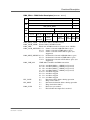
1
Embedded Solutions
20A014-00 E2 – 2007-08-16
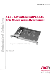
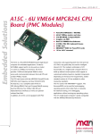
A14C – 6U VME64
MPC8540 SBC / PMC
Configuration example
User Manual
®
A14C – 6U VME64 MPC8540 SBC / PMC
A14C – 6U VME64 MPC8540 SBC / PMC
The A14C is an advanced PowerPC® based single-board computer for embedded
applications. It features full VME64 support and it can be used as a master or a slave
in a VMEbus environment. The A14C provides 1 MB local shared SRAM for slave
access and communication between the local CPU and another VMEbus master.
The A14C is controlled by an MPC8540 integrated PowerPC® processor working
at 800 MHz. The SBC is equipped with a DDR SO-DIMM socket for data storage,
with NAND Flash for program storage as well as with non-volatile FRAM. The
board provides front-panel access for two Gigabit Ethernet, one fast Ethernet and
one COM via four RJ45 connectors. Four more UARTs are optionally accessible via
SA-Adapters™ for front connection.
Additional functionality such as graphics, touch, CAN, binary I/O etc. can be
realized as IP cores in FPGA for the needs of the individual application. The
corresponding PHYs are available via SA-Adapters™ on a transition module to the
rear.
The FPGA acts as a standard PCI device on the A14C. The FPGA functions are
loaded by software during power-up within less than 1 s. FPGA updates can be
carried out dynamically during operation.
In addition, the A14C can be equipped with PMC mezzanine cards supporting
64 bits/66 MHz as well as front I/O and rear I/O (PIM).
The A14C comes with MENMON™ support. This firmware/BIOS can be used for
bootstrapping operating systems (from disk, Flash or network), for hardware testing,
or for debugging applications without running any operating system.
MEN Mikro Elektronik GmbH
20A014-00 E2 – 2007-08-16
2
Technical Data
Technical Data
CPU
• PowerPC®
- MPC8540 PowerQUICC™ III
- 800MHz (666..833MHz optional)
- e500 PowerPC® core with SPE APU and MMU
- Integrated Northbridge and Southbridge
- High memory bandwidth
Memory
• 2x32KB L1 data and instruction cache, 256KB L2 cache / SRAM integrated in
MPC8540
• Up to 2GB SDRAM system memory
- SO-DIMM slot for SDRAM modules
- DDR2100 with or without ECC
- 133MHz memory bus frequency
• Up to 1GB soldered NAND Flash (and more), FPGA-controlled
• Up to 16MB additional SDRAM, FPGA-controlled, e.g. for video data and
NAND Flash firmware
• 8MB boot Flash
• 32KB non-volatile FRAM
• Serial EEPROM 4kbits for factory settings
Mass Storage
• Parallel IDE (PATA)
- One port for hard-disk drives
- Drive can be connected via ribbon cable or mounted directly on the CPU
board using MEN adapter kit (instead of PMC modules)
- Only one VMEbus slot needed even with hard disk
- PIO mode 0 support
• Up to 1GB soldered ATA NAND Flash (and more), FPGA-controlled
I/O
• Three Ethernet channels
- Two 10/100/1000Base-T Ethernet channels
- One 10/100Base-T Ethernet channel
- Three RJ45 connectors at front panel
- Two on-board LEDs to signal LAN Link and Activity
• One RS232 UART (COM1)
- One RJ45 connector at front panel
- Data rates up to 115.2kbits/s
- 16-byte transmit/receive buffer
- Handshake lines: CTS, RTS
MEN Mikro Elektronik GmbH
20A014-00 E2 – 2007-08-16
3
Technical Data
• One LVTTL UART (COM10)
- FPGA-controlled
- Accessible via rear I/O
- Data rates up to 115.2kbits/s
- 60-byte transmit/receive buffers
- Handshake lines: CTS, RTS; DCD, DSR, DTR; RI
• Quad UART (COM20..COM23)
- Physical interface using SA-Adapters™ via 10-pin ribbon cable on I/O connector
- RS232..RS485, isolated or not: for free use in system (e. g. cable to front)
- Data rates up to 115.2kbits/s
- 128-byte transmit/receive buffer
- Handshake lines: CTS, RTS; DCD, DSR, DTR; RI
• GPIO
- 39 GPIO lines
- FPGA-controlled
- Accessible via rear I/O
Front Connections
• Three Ethernet (RJ45)
• COM1 (RJ45)
• COM20..COM23 (optional, instead of PMC modules, or in second front-panel
slot)
• PMC 0 and 1
Rear I/O
• COM10
• GPIO
• Mezzanine rear I/O: PMC 0
FPGA
• Standard factory FPGA configuration:
- Main bus interface
- 16Z070_IDEDISK - IDE controller for NAND Flash
- 16Z043_SDRAM - Additional SDRAM controller (16MB)
- 16Z023_IDENHS - IDE controller (PIO mode 0; non-hot-swap)
- 16Z025_UART - UART controller (controls COM10)
- 16Z034_GPIO - GPIO controller (40 lines, 5 IP cores)
• The FPGA offers the possibility to add customized I/O functionality. See FPGA.
Mezzanine Slots
• Two PMC slots
- Compliant with PMC standard IEEE 1386.1
- Up to 64-bit/64-MHz, 3.3V V(I/O)
- PMC I/O module (PIM) support through J4
MEN Mikro Elektronik GmbH
20A014-00 E2 – 2007-08-16
4
Technical Data
Miscellaneous
• Real-time clock with GoldCap backup
• Power supervision and watchdog
• Reset button, GPIO-controlled, in ejector handle
Local PCI Bus
• 32-bit/33-MHz, 3.3V V(I/O)
• Compliant with PCI Specification 2.2
VMEbus
• Compliant with VME64 Specification
• Slot-1 function with auto-detection
• Master
- D08(EO):D16:D32:D64:A16:A24:A32:ADO:BLT:RMW
• Slave
- D08(EO):D16:D32:D64:A16:A24:A32:BLT:RMW
• 1MB shared fast SRAM
• DMA
• Mailbox functionality
• Interrupter D08(O):I(7-1):ROAK
• Interrupt handler D08(O):IH(7-1)
• Single level 3 fair requester
• Single level 3 arbiter
• Bus timer
• Location Monitor
• Performance
- Coupled read/write D32 non-block transfer rate 6.5 MB/s
- DMA read/write D32 BLT transfer rate 12.1 MB/s
- DMA read/write D64 MBLT transfer rate 25 MB/s
Electrical Specifications
• Supply voltage/power consumption:
- +5V (-3%/+5%), 3A typ.
- +12V (-5%/+5%), only provided for PMCs that need 12V
- -12V (-5%/+5%), only provided for PMCs that need 12V
• MTBF: 92,800h @ 40°C (derived from MIL-HDBK-217F)
Mechanical Specifications
• Dimensions: standard double Eurocard, 233.3mm x 160mm
• Weight (without PMC modules): 450g
MEN Mikro Elektronik GmbH
20A014-00 E2 – 2007-08-16
5
Technical Data
Environmental Specifications
• Temperature range (operation):
- 0..+60°C
- Airflow: min. 10m³/h
• Temperature range (storage): -40..+85°C
• Relative humidity (operation): max. 95% non-condensing
• Relative humidity (storage): max. 95% non-condensing
• Altitude: -300m to + 3,000m
• Shock: 15g/11ms
• Bump: 10g/16ms
• Vibration (sinusoidal): 2g/10..150Hz
• Conformal coating on request
Safety
• PCB manufactured with a flammability rating of 94V-0 by UL recognized manufacturers
EMC
• Tested according to EN 55022 (radio disturbance), IEC1000-4-2 (ESD) and
IEC1000-4-4 (burst) with regard to CE conformity
BIOS
• MENMON™
Software Support
•
•
•
•
VxWorks®
Linux (ELinOS)
QNX®
For more information on supported operating system versions and drivers see
online data sheet.
MEN Mikro Elektronik GmbH
20A014-00 E2 – 2007-08-16
6
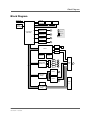
Block Diagram
Block Diagram
SDRAM
Main
(SO-DIMM)
EEPROM
Boot Flash
FRAM
RTC
Watchdog
PowerPC®
MPC8540
Ethernet
1000Base-T
F
Ethernet
1000Base-T
F
Ethernet
100Base-T
F
RS232 COM1
F
F Front Panel
R Rear I/O
B On Board
Option
IDE
FPGA
B
COM10
GPIO
SDRAM
Additional
Quad UART
COM20..23
PCI
NAND
Flash
B
SA
F
SA
F
SA
F
SA
F
PMC 1
VME
P2
R
F
PCI-toPCI
Bridge
PMC 0
F
SSRAM
VME
P1
PCI-to-VMEbus
Bridge
MEN Mikro Elektronik GmbH
20A014-00 E2 – 2007-08-16
7
Configuration Options
Configuration Options
CPU
• Type
- MPC8540
- MPC8560
• Clock
- 666..833 MHz
Memory
• System RAM
- 256 MB, 512 MB, 1 GB or 2 GB
- With or without ECC
• NAND Flash
- 0 MB up to maximum available
• Additional SDRAM
- 0 MB or 16 MB
• FRAM
- 0 MB or 32 MB
• Boot Flash
- 8 MB or 16 MB
I/O
• Quad UART (COM20..23)
- Direct on-board connection via 10-pin connectors, instead of PMCs
• Front Connections
- D-Sub instead of RJ45 connectors
Mezzanine Slots
• 2 PMC
• 3 PC-MIP®
Operation Temperature
• 0..+60°C
Please note that some of these options may only be available for large volumes.
Please ask our sales staff for more information.
MEN Mikro Elektronik GmbH
20A014-00 E2 – 2007-08-16
8
FPGA
FPGA
FPGA Capabilities
• FPGA Altera® Cyclone™ EP1C12
- 12,060 logic elements
- 239,616 total RAM bits
• Connection
- Available pin count: 47 pins
- Functions available e.g. via I/O connector
Flexible Configuration
• This MEN board offers the possibility to add customized I/O functionality in
FPGA.
• It depends on the board type, pin counts and number of logic elements which IP
cores make sense and/or can be implemented. Please contact MEN for information on feasibility.
• Depending on the hardware platform, SA-Adapters™ can be used to realize the
physical lines.
MEN IP Cores
• MEN has a large number of standard IP cores to choose from.
• Examples:
- IDE (e.g. PIO mode 0, UDMA mode 5)
- UARTs
- CAN bus
- Display control
- ...
• For IP cores developed by MEN please refer to our IP core overview.
- IP Core compare chart (PDF)
• MEN also offers development of new (customized) IP cores.
Third-Party IP Cores
• Third-party IP cores can also be used in combination with MEN IP cores.
• Examples:
- www.altera.com
- www.opencores.org
FPGA Design Environment
• Altera® offers free download of Quartus® II Web Edition
- Complete environment for FPGA and CPLD design
- Includes schematic- and text-based design entry
- Integrated VHDL and Verilog HDL synthesis and support for third-party synthesis software
- SOPC Builder system generation software
- Place-and-route, verification, and programming
» Altera® Quartus® II Web Edition FPGA design tool
MEN Mikro Elektronik GmbH
20A014-00 E2 – 2007-08-16
9
Product Safety
Product Safety
!
Electrostatic Discharge (ESD)
Computer boards and components contain electrostatic sensitive devices.
Electrostatic discharge (ESD) can damage components. To protect the board and
other components against damage from static electricity, you should follow some
precautions whenever you work on your computer.
• Power down and unplug your computer system when working on the inside.
• Hold components by the edges and try not to touch the IC chips, leads, or circuitry.
• Use a grounded wrist strap before handling computer components.
• Place components on a grounded antistatic pad or on the bag that came with the
component whenever the components are separated from the system.
• Store the board only in its original ESD-protected packaging. Retain the original
packaging in case you need to return the board to MEN for repair.
MEN Mikro Elektronik GmbH
20A014-00 E2 – 2007-08-16
10
About this Document
About this Document
This user manual describes the hardware functions of the board, connection of
peripheral devices and integration into a system. It also provides additional
information for special applications and configurations of the board.
The manual does not include detailed information on individual components (data
sheets etc.). A list of literature is given in the appendix.
History
Edition
Comments
Technical Content
Date of Issue
E1
First edition
H. Schubert, D. Hofbauer, T. Schnürer
2006-01-17
E2
General update, switching of
rear I/O documented, address
table adapted to MENMON
rev. 1.7
H. Schubert, D. Hofbauer, T. Schnürer
2007-08-16
Conventions
!
italics
bold
monospace
hyperlink
This sign marks important notes or warnings concerning proper functionality of the
product described in this document. You should read them in any case.
Folder, file and function names are printed in italics.
Bold type is used for emphasis.
A monospaced font type is used for hexadecimal numbers, listings, C function
descriptions or wherever appropriate. Hexadecimal numbers are preceded by "0x".
Hyperlinks are printed in blue color.
The globe will show you where hyperlinks lead directly to the Internet, so you can
look for the latest information online.
IRQ#
/IRQ
Signal names followed by "#" or preceded by a slash ("/") indicate that this signal is
either active low or that it becomes active at a falling edge.
in/out
Signal directions in signal mnemonics tables generally refer to the corresponding
board or component, "in" meaning "to the board or component", "out" meaning
"coming from it".
Vertical lines on the outer margin signal technical changes to the previous edition of
the document.
MEN Mikro Elektronik GmbH
20A014-00 E2 – 2007-08-16
11
About this Document
Legal Information
MEN Mikro Elektronik reserves the right to make changes without further notice to any products herein. MEN makes no
warranty, representation or guarantee regarding the suitability of its products for any particular purpose, nor does MEN assume
any liability arising out of the application or use of any product or circuit, and specifically disclaims any and all liability,
including without limitation consequential or incidental damages.
"Typical" parameters can and do vary in different applications. All operating parameters, including "Typicals" must be
validated for each customer application by customer's technical experts.
MEN does not convey any license under its patent rights nor the rights of others.
Unless agreed otherwise, MEN products are not designed, intended, or authorized for use as components in systems intended
for surgical implant into the body, or other applications intended to support or sustain life, or for any other application in which
the failure of the MEN product could create a situation where personal injury or death may occur. Should Buyer purchase or
use MEN products for any such unintended or unauthorized application, Buyer shall indemnify and hold MEN and its officers,
employees, subsidiaries, affiliates, and distributors harmless against all claims, costs, damages, and expenses, and reasonable
attorney fees arising out of, directly or indirectly, any claim of personal injury or death associated with such unintended or
unauthorized use, even if such claim alleges that MEN was negligent regarding the design or manufacture of the part.
Unless agreed otherwise, the products of MEN Mikro Elektronik are not suited for use in nuclear reactors and for application
in medical appliances used for therapeutical purposes. Application of MEN products in such plants is only possible after the
user has precisely specified the operation environment and after MEN Mikro Elektronik has consequently adapted and
released the product.
ESM™, MDIS™, MDIS4™, MENMON™, M-Module™, M-Modules™, SA-Adapter™, SA-Adapters™, UBox™ and
USM™ are trademarks of MEN Mikro Elektronik GmbH. PC-MIP® is a registered trademark of MEN Micro, Inc. and SBS
Technologies, Inc. MEN Mikro Elektronik®, ESMexpress® and the MEN logo are registered trademarks of MEN Mikro
Elektronik GmbH.
Altera®, Avalon®, Cyclone™, Nios® and Quartus® are trademarks or registered trademarks of Altera Corp.
Freescale™ and PowerQUICC™ are trademarks of Freescale Semiconductor, Inc.
PowerPC® is a registered trademark of IBM Corp.
Microsoft® and Windows® are registered trademarks of Microsoft Corp. Windows® Vista™ is a trademark of Microsoft Corp.
OS-9®, OS-9000® and SoftStax® are registered trademarks of RadiSys Microware Communications Software Division, Inc.
FasTrak™ and Hawk™ are trademarks of RadiSys Microware Communications Software Division, Inc. RadiSys® is a
registered trademark of RadiSys Corporation.
QNX® is a registered trademark of QNX Ltd.
CompactFlash® is a registered trademark of SanDisk Corp.
Tornado® and VxWorks® are registered trademarks of Wind River Systems, Inc.
All other products or services mentioned in this publication are identified by the trademarks, service marks, or product names
as designated by the companies who market those products. The trademarks and registered trademarks are held by the
companies producing them. Inquiries concerning such trademarks should be made directly to those companies. All other brand
or product names are trademarks or registered trademarks of their respective holders.
Information in this document has been carefully checked and is believed to be accurate as of the date of publication; however,
no responsibility is assumed for inaccuracies. MEN Mikro Elektronik accepts no liability for consequential or incidental
damages arising from the use of its products and reserves the right to make changes on the products herein without notice to
improve reliability, function or design. MEN Mikro Elektronik does not assume any liability arising out of the application or
use of the products described in this document.
Copyright © 2007 MEN Mikro Elektronik GmbH. All rights reserved.
Please recycle
Germany
MEN Mikro Elektronik GmbH
Neuwieder Straße 5-7
90411 Nuremberg
Phone +49-911-99 33 5-0
Fax +49-911-99 33 5-901
E-mail [email protected]
www.men.de
MEN Mikro Elektronik GmbH
20A014-00 E2 – 2007-08-16
France
MEN Mikro Elektronik SA
18, rue René Cassin
ZA de la Châtelaine
74240 Gaillard
Phone +33 (0) 450-955-312
Fax +33 (0) 450-955-211
E-mail [email protected]
www.men-france.fr
USA
MEN Micro, Inc.
24 North Main Street
Ambler, PA 19002
Phone (215) 542-9575
Fax (215) 542-9577
E-mail [email protected]
www.menmicro.com
12
Contents
Contents
1 Getting Started . . . . . . . . . . . . . . . . . . . . . . . . . . . . . . . . . . . . . . . . . . . . . . . .
1.1 Maps of the Board . . . . . . . . . . . . . . . . . . . . . . . . . . . . . . . . . . . . . . . .
1.2 Configuring the Hardware . . . . . . . . . . . . . . . . . . . . . . . . . . . . . . . . . .
1.3 Integrating the Board into a System . . . . . . . . . . . . . . . . . . . . . . . . . .
1.4 Installing Operating System Software. . . . . . . . . . . . . . . . . . . . . . . . .
19
19
21
22
23
2 Functional Description . . . . . . . . . . . . . . . . . . . . . . . . . . . . . . . . . . . . . . . . . .
2.1 Power Supply. . . . . . . . . . . . . . . . . . . . . . . . . . . . . . . . . . . . . . . . . . . .
2.1.1
Watchdog. . . . . . . . . . . . . . . . . . . . . . . . . . . . . . . . . . . . . . . .
2.2 Clock Supply . . . . . . . . . . . . . . . . . . . . . . . . . . . . . . . . . . . . . . . . . . . .
2.3 Real-Time Clock . . . . . . . . . . . . . . . . . . . . . . . . . . . . . . . . . . . . . . . . .
2.4 PowerPC CPU . . . . . . . . . . . . . . . . . . . . . . . . . . . . . . . . . . . . . . . . . . .
2.4.1
General . . . . . . . . . . . . . . . . . . . . . . . . . . . . . . . . . . . . . . . . .
2.4.2
Thermal Considerations . . . . . . . . . . . . . . . . . . . . . . . . . . . .
2.5 Bus Structure . . . . . . . . . . . . . . . . . . . . . . . . . . . . . . . . . . . . . . . . . . . .
2.5.1
Host-to-PCI Bridge . . . . . . . . . . . . . . . . . . . . . . . . . . . . . . . .
2.5.2
Local PCI Bus . . . . . . . . . . . . . . . . . . . . . . . . . . . . . . . . . . . .
2.5.3
PCI-to-PCI Bridge. . . . . . . . . . . . . . . . . . . . . . . . . . . . . . . . .
2.5.4
PCI-to-VMEbus Bridge . . . . . . . . . . . . . . . . . . . . . . . . . . . .
2.6 Memory . . . . . . . . . . . . . . . . . . . . . . . . . . . . . . . . . . . . . . . . . . . . . . . .
2.6.1
DRAM System Memory . . . . . . . . . . . . . . . . . . . . . . . . . . . .
2.6.2
Boot Flash . . . . . . . . . . . . . . . . . . . . . . . . . . . . . . . . . . . . . . .
2.6.3
NAND Flash . . . . . . . . . . . . . . . . . . . . . . . . . . . . . . . . . . . . .
2.6.4
FRAM . . . . . . . . . . . . . . . . . . . . . . . . . . . . . . . . . . . . . . . . . .
2.6.5
Additional SDRAM . . . . . . . . . . . . . . . . . . . . . . . . . . . . . . .
2.6.6
EEPROM. . . . . . . . . . . . . . . . . . . . . . . . . . . . . . . . . . . . . . . .
2.7 IDE Interface . . . . . . . . . . . . . . . . . . . . . . . . . . . . . . . . . . . . . . . . . . . .
2.7.1
Connection . . . . . . . . . . . . . . . . . . . . . . . . . . . . . . . . . . . . . .
2.7.2
Installing a Hard Disk . . . . . . . . . . . . . . . . . . . . . . . . . . . . . .
2.8 Ethernet Interfaces. . . . . . . . . . . . . . . . . . . . . . . . . . . . . . . . . . . . . . . .
2.8.1
Connection . . . . . . . . . . . . . . . . . . . . . . . . . . . . . . . . . . . . . .
2.8.2
General . . . . . . . . . . . . . . . . . . . . . . . . . . . . . . . . . . . . . . . . .
2.8.3
10Base-T . . . . . . . . . . . . . . . . . . . . . . . . . . . . . . . . . . . . . . . .
2.8.4
100Base-T . . . . . . . . . . . . . . . . . . . . . . . . . . . . . . . . . . . . . . .
2.8.5
1000Base-T . . . . . . . . . . . . . . . . . . . . . . . . . . . . . . . . . . . . . .
2.9 UART COM1 Interface . . . . . . . . . . . . . . . . . . . . . . . . . . . . . . . . . . . .
2.10 UART COM10 Interface . . . . . . . . . . . . . . . . . . . . . . . . . . . . . . . . . . .
2.11 UART COM20..COM23 Interfaces. . . . . . . . . . . . . . . . . . . . . . . . . . .
2.11.1 Connection via 40-pin Connector . . . . . . . . . . . . . . . . . . . . .
2.11.2 Connection via 10-pin SA-Adapter Connectors . . . . . . . . . .
2.12 GPIO . . . . . . . . . . . . . . . . . . . . . . . . . . . . . . . . . . . . . . . . . . . . . . . . . .
2.13 PMC Slots . . . . . . . . . . . . . . . . . . . . . . . . . . . . . . . . . . . . . . . . . . . . . .
2.13.1 Installing a PMC Mezzanine Module . . . . . . . . . . . . . . . . . .
24
24
24
24
24
25
25
25
26
26
26
26
26
27
27
27
27
27
27
27
28
28
30
32
32
34
34
34
34
35
37
38
39
42
45
46
47
MEN Mikro Elektronik GmbH
20A014-00 E2 – 2007-08-16
13
Contents
2.14 Board-to-Board I/O Connector . . . . . . . . . . . . . . . . . . . . . . . . . . . . . .
2.15 Reset Button . . . . . . . . . . . . . . . . . . . . . . . . . . . . . . . . . . . . . . . . . . . .
2.16 VMEbus Interface . . . . . . . . . . . . . . . . . . . . . . . . . . . . . . . . . . . . . . . .
2.16.1 PCI Configuration Space Registers. . . . . . . . . . . . . . . . . . . .
2.16.2 Runtime Registers . . . . . . . . . . . . . . . . . . . . . . . . . . . . . . . . .
2.16.3 VMEbus Master Mapping. . . . . . . . . . . . . . . . . . . . . . . . . . .
2.16.4 VME Slave Mapping. . . . . . . . . . . . . . . . . . . . . . . . . . . . . . .
2.16.5 SRAM . . . . . . . . . . . . . . . . . . . . . . . . . . . . . . . . . . . . . . . . . .
2.16.6 Slot-1 Function . . . . . . . . . . . . . . . . . . . . . . . . . . . . . . . . . . .
2.16.7 VMEbus Master Interface . . . . . . . . . . . . . . . . . . . . . . . . . . .
2.16.8 VMEbus Slave Interface . . . . . . . . . . . . . . . . . . . . . . . . . . . .
2.16.9 VMEbus Requester . . . . . . . . . . . . . . . . . . . . . . . . . . . . . . . .
2.16.10 VMEbus Interrupt Handler . . . . . . . . . . . . . . . . . . . . . . . . . .
2.16.11 VMEbus Interrupter . . . . . . . . . . . . . . . . . . . . . . . . . . . . . . .
2.16.12 A32 Address Mode . . . . . . . . . . . . . . . . . . . . . . . . . . . . . . . .
2.16.13 Mailbox . . . . . . . . . . . . . . . . . . . . . . . . . . . . . . . . . . . . . . . . .
2.16.14 Location Monitor . . . . . . . . . . . . . . . . . . . . . . . . . . . . . . . . .
2.16.15 DMA Controller . . . . . . . . . . . . . . . . . . . . . . . . . . . . . . . . . .
2.16.16 Connection . . . . . . . . . . . . . . . . . . . . . . . . . . . . . . . . . . . . . .
48
51
52
53
54
55
56
56
57
58
62
67
68
69
70
71
72
74
76
3 FPGA . . . . . . . . . . . . . . . . . . . . . . . . . . . . . . . . . . . . . . . . . . . . . . . . . . . . . . . .
3.1 General . . . . . . . . . . . . . . . . . . . . . . . . . . . . . . . . . . . . . . . . . . . . . . . .
3.2 System Unit . . . . . . . . . . . . . . . . . . . . . . . . . . . . . . . . . . . . . . . . . . . . .
3.2.1
Functional Description . . . . . . . . . . . . . . . . . . . . . . . . . . . . .
3.2.2
Address Organization . . . . . . . . . . . . . . . . . . . . . . . . . . . . . .
3.3 Standard Factory FPGA Configuration . . . . . . . . . . . . . . . . . . . . . . . .
3.3.1
IP Cores. . . . . . . . . . . . . . . . . . . . . . . . . . . . . . . . . . . . . . . . .
3.3.2
FPGA Configuration Table . . . . . . . . . . . . . . . . . . . . . . . . . .
82
82
83
83
85
92
92
92
4 MENMON . . . . . . . . . . . . . . . . . . . . . . . . . . . . . . . . . . . . . . . . . . . . . . . . . . . . 93
4.1 General . . . . . . . . . . . . . . . . . . . . . . . . . . . . . . . . . . . . . . . . . . . . . . . . 93
4.1.1
State Diagram . . . . . . . . . . . . . . . . . . . . . . . . . . . . . . . . . . . . 94
4.2 Interacting with MENMON . . . . . . . . . . . . . . . . . . . . . . . . . . . . . . . . 96
4.2.1
Entering the Setup Menu/Command Line . . . . . . . . . . . . . . 96
4.3 Configuring MENMON for Automatic Boot . . . . . . . . . . . . . . . . . . . 96
4.4 Updating Boot Flash and NAND Flash . . . . . . . . . . . . . . . . . . . . . . . . 97
4.4.1
Update via the Serial Console using SERDL . . . . . . . . . . . . 97
4.4.2
Update from Network using NDL. . . . . . . . . . . . . . . . . . . . . 97
4.4.3
Update via Program Update Menu . . . . . . . . . . . . . . . . . . . . 97
4.4.4
Automatic Update Check . . . . . . . . . . . . . . . . . . . . . . . . . . . 98
4.5 Diagnostic Tests. . . . . . . . . . . . . . . . . . . . . . . . . . . . . . . . . . . . . . . . . . 99
4.5.1
Ethernet . . . . . . . . . . . . . . . . . . . . . . . . . . . . . . . . . . . . . . . . . 99
4.5.2
SDRAM and FRAM . . . . . . . . . . . . . . . . . . . . . . . . . . . . . . 100
4.5.3
EEPROM. . . . . . . . . . . . . . . . . . . . . . . . . . . . . . . . . . . . . . . 101
4.5.4
IDE/NAND Flash . . . . . . . . . . . . . . . . . . . . . . . . . . . . . . . . 102
MEN Mikro Elektronik GmbH
20A014-00 E2 – 2007-08-16
14
Contents
4.5.5
COM1 Port . . . . . . . . . . . . . . . . . . . . . . . . . . . . . . . . . . . . .
4.5.6
Primary/Secondary MENMON. . . . . . . . . . . . . . . . . . . . . .
4.5.7
Hardware Monitor Test . . . . . . . . . . . . . . . . . . . . . . . . . . . .
4.5.8
RTC . . . . . . . . . . . . . . . . . . . . . . . . . . . . . . . . . . . . . . . . . . .
4.6 MENMON Configuration and Organization . . . . . . . . . . . . . . . . . . .
4.6.1
Consoles . . . . . . . . . . . . . . . . . . . . . . . . . . . . . . . . . . . . . . .
4.6.2
Video Modes . . . . . . . . . . . . . . . . . . . . . . . . . . . . . . . . . . . .
4.6.3
Abort Pin . . . . . . . . . . . . . . . . . . . . . . . . . . . . . . . . . . . . . . .
4.6.4
MENMON Memory Map . . . . . . . . . . . . . . . . . . . . . . . . . .
4.6.5
MENMON BIOS Logical Units . . . . . . . . . . . . . . . . . . . . .
4.6.6
System Parameters . . . . . . . . . . . . . . . . . . . . . . . . . . . . . . .
4.7 MENMON Commands . . . . . . . . . . . . . . . . . . . . . . . . . . . . . . . . . . .
102
103
103
103
104
104
104
104
105
106
107
113
5 Organization of the Board . . . . . . . . . . . . . . . . . . . . . . . . . . . . . . . . . . . . . .
5.1 Memory Mappings . . . . . . . . . . . . . . . . . . . . . . . . . . . . . . . . . . . . . .
5.2 Interrupt Handling . . . . . . . . . . . . . . . . . . . . . . . . . . . . . . . . . . . . . . .
5.3 SMB Devices . . . . . . . . . . . . . . . . . . . . . . . . . . . . . . . . . . . . . . . . . . .
5.4 PCI Devices on Bus 0 . . . . . . . . . . . . . . . . . . . . . . . . . . . . . . . . . . . .
115
115
116
116
117
6 Appendix . . . . . . . . . . . . . . . . . . . . . . . . . . . . . . . . . . . . . . . . . . . . . . . . . . . .
6.1 Literature and Web Resources . . . . . . . . . . . . . . . . . . . . . . . . . . . . . .
6.1.1
PowerPC . . . . . . . . . . . . . . . . . . . . . . . . . . . . . . . . . . . . . . .
6.1.2
IDE . . . . . . . . . . . . . . . . . . . . . . . . . . . . . . . . . . . . . . . . . . .
6.1.3
Ethernet . . . . . . . . . . . . . . . . . . . . . . . . . . . . . . . . . . . . . . . .
6.1.4
PMC . . . . . . . . . . . . . . . . . . . . . . . . . . . . . . . . . . . . . . . . . .
6.1.5
PCI-104 . . . . . . . . . . . . . . . . . . . . . . . . . . . . . . . . . . . . . . . .
6.1.6
VMEbus . . . . . . . . . . . . . . . . . . . . . . . . . . . . . . . . . . . . . . .
6.2 Finding out the Board’s Article Number, Revision and Serial
Number . . . . . . . . . . . . . . . . . . . . . . . . . . . . . . . . . . . . . . . . . . . . . . .
118
118
118
118
118
119
119
119
MEN Mikro Elektronik GmbH
20A014-00 E2 – 2007-08-16
119
15
Figures
Figure 1. Map of the Board – front view . . . . . . . . . . . . . . . . . . . . . . . . . . . . . . . 19
Figure 2. Map of the Board – top view . . . . . . . . . . . . . . . . . . . . . . . . . . . . . . . . 20
Figure 3. Position of fuse for IDE protection. . . . . . . . . . . . . . . . . . . . . . . . . . . . 29
Figure 4. Installing SA-Adapters on A14C directly . . . . . . . . . . . . . . . . . . . . . . 43
Figure 5. Position of fuse for COM20..COM23 protection . . . . . . . . . . . . . . . . . 44
Figure 6. Installing a PMC mezzanine module . . . . . . . . . . . . . . . . . . . . . . . . . . 47
Figure 7. Position of reset button . . . . . . . . . . . . . . . . . . . . . . . . . . . . . . . . . . . . . 51
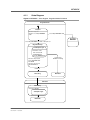
Figure 8. FPGA – Block diagram . . . . . . . . . . . . . . . . . . . . . . . . . . . . . . . . . . . . 82
Figure 9. MENMON – State diagram, Degraded Mode/Full Mode . . . . . . . . . . 94
Figure 10. MENMON – State diagram, Main State . . . . . . . . . . . . . . . . . . . . . . . 95
Figure 11. Label giving the board’s article number, revision and serial number 119
MEN Mikro Elektronik GmbH
20A014-00 E2 – 2007-08-16
16
Tables
Table 1.
Table 2.
Table 3.
Table 4.
Table 5.
Table 6.
Table 7.
Table 8.
Table 9.
Table 10.
Table 11.
Table 12.
Table 13.
Table 14.
Table 15.
Table 16.
Table 17.
Table 18.
Table 19.
Table 20.
Table 21.
Table 22.
Table 23.
Table 24.
Table 25.
Table 26.
Table 27.
Table 28.
Table 29.
Table 30.
Table 31.
Table 32.
Table 33.
Table 34.
Table 35.
MEN Mikro Elektronik GmbH
20A014-00 E2 – 2007-08-16
Pin assignment of 44-pin IDE plug connector . . . . . . . . . . . . . . . . . . . 28
Signal mnemonics of 44-pin IDE plug connector . . . . . . . . . . . . . . . . 29
Signal mnemonics of Ethernet 10Base-T/100Base-TX/1000Base-TX
interfaces. . . . . . . . . . . . . . . . . . . . . . . . . . . . . . . . . . . . . . . . . . . . . . . . 32
Pin assignment of 8-pin RJ45 Ethernet 10Base-T/100Base-TX/
1000Base-TX connectors (LAN1..3) . . . . . . . . . . . . . . . . . . . . . . . . . . 32
Pin assignment of 9-pin D-Sub 10Base-T/100Base-TX plug connector
(LAN1 and LAN2) . . . . . . . . . . . . . . . . . . . . . . . . . . . . . . . . . . . . . . . . 33
Pin assignment of 9-pin D-Sub 10Base-T/100Base-TX plug connector
(LAN3 and COM1) . . . . . . . . . . . . . . . . . . . . . . . . . . . . . . . . . . . . . . . 33
Signal mnemonics of UART COM1 interface . . . . . . . . . . . . . . . . . . . 35
Pin assignment of 8-pin RJ45 UART connector (COM1) . . . . . . . . . . 35
Pin assignment of 9-pin D-Sub COM1/LAN3 plug connector . . . . . . 36
Signal mnemonics for UART COM20..COM23 interfaces . . . . . . . . . 38
Pin assignment of the 40-pin UART COM20..COM23 connector . . . 39
Pin assignment of the 10-pin UART COM20..COM23 connectors. . . 42
Assignment of 16Z034_GPIO controllers . . . . . . . . . . . . . . . . . . . . . . 45
Pin assignment of I/O connector J2 – factory standard FPGA
configuration. . . . . . . . . . . . . . . . . . . . . . . . . . . . . . . . . . . . . . . . . . . . . 49
Signal mnemonics of I/O connector J2 – factory standard FPGA
configuration. . . . . . . . . . . . . . . . . . . . . . . . . . . . . . . . . . . . . . . . . . . . . 50
VMEbus interface PCI configuration space registers. . . . . . . . . . . . . . 53
VMEbus runtime registers . . . . . . . . . . . . . . . . . . . . . . . . . . . . . . . . . . 54
VMEbus interface BAR 0. . . . . . . . . . . . . . . . . . . . . . . . . . . . . . . . . . . 55
VMEbus interface BAR1 . . . . . . . . . . . . . . . . . . . . . . . . . . . . . . . . . . . 55
VMEbus interface BAR2 . . . . . . . . . . . . . . . . . . . . . . . . . . . . . . . . . . . 55
VMEbus interface BAR3 . . . . . . . . . . . . . . . . . . . . . . . . . . . . . . . . . . . 55
VMEbus interface BAR4 . . . . . . . . . . . . . . . . . . . . . . . . . . . . . . . . . . . 55
VMEbus slave address windows . . . . . . . . . . . . . . . . . . . . . . . . . . . . . 56
VMEbus interface valid combinations for byte enables supported by PCIto-VME bridge . . . . . . . . . . . . . . . . . . . . . . . . . . . . . . . . . . . . . . . . . . . 59
VMEbus master Address Modifier codes. . . . . . . . . . . . . . . . . . . . . . . 61
VMEbus slave Address Modifier codes . . . . . . . . . . . . . . . . . . . . . . . . 66
Pin assignment of VME64 connector P1 . . . . . . . . . . . . . . . . . . . . . . . 76
Pin assignment of VMEbus rear I/O connector P2 – PMC signals . . . 78
Signal mnemonics of VMEbus rear I/O connector P2 – PMC 0 . . . . . 79
Pin assignment of VMEbus rear I/O connector P2 – FPGA I/O signals80
Signal mnemonics of VMEbus rear I/O connector P2 – FPGA I/O. . . 81
FPGA – Address map . . . . . . . . . . . . . . . . . . . . . . . . . . . . . . . . . . . . . . 85
FPGA – Factory standard configuration table for A14C . . . . . . . . . . . 92
MENMON – Program update files and locations . . . . . . . . . . . . . . . . 97
MENMON – Diagnostic tests: Ethernet. . . . . . . . . . . . . . . . . . . . . . . . 99
17
Table 36.
Table 37.
Table 38.
Table 39.
Table 40.
Table 41.
Table 42.
Table 43.
Table 44.
Table 45.
Table 46.
Table 47.
Table 48.
Table 49.
Table 50.
Table 51.
Table 52.
Table 53.
Table 54.
Table 55.
Table 56.
Table 57.
Table 58.
Table 59.
Table 60.
MEN Mikro Elektronik GmbH
20A014-00 E2 – 2007-08-16
MENMON – Diagnostic tests: SDRAM and FRAM . . . . . . . . . . . . .
MENMON – Diagnostic tests: EEPROM . . . . . . . . . . . . . . . . . . . . .
MENMON – Diagnostic tests: IDE/NAND Flash . . . . . . . . . . . . . . .
MENMON – Diagnostic tests: COM1 Port . . . . . . . . . . . . . . . . . . . .
MENMON – Diagnostic tests: Primary/Secondary MENMON . . . .
MENMON – Diagnostic tests: Hardware Monitor. . . . . . . . . . . . . . .
MENMON – Diagnostic tests: RTC. . . . . . . . . . . . . . . . . . . . . . . . . .
MENMON – System parameters for console selection . . . . . . . . . . .
MENMON – Address map (full-featured mode) . . . . . . . . . . . . . . . .
MENMON – Boot Flash memory map . . . . . . . . . . . . . . . . . . . . . . .
MENMON – Controller Logical Units (CLUNs). . . . . . . . . . . . . . . .
MENMON – Device Logical Units (DLUNs) . . . . . . . . . . . . . . . . . .
MENMON – A14C system parameters – autodetected parameters . .
MENMON – A14C system parameters – production data. . . . . . . . .
MENMON – A14C system parameters – MENMON persistent
parameters. . . . . . . . . . . . . . . . . . . . . . . . . . . . . . . . . . . . . . . . . . . . . .
MENMON – A14C system parameters – VxWorks bootline
parameters. . . . . . . . . . . . . . . . . . . . . . . . . . . . . . . . . . . . . . . . . . . . . .
MENMON – Reset causes through system parameter rststat. . . . . . .
MENMON – Voltage limits through system parameter psrXXX . . .
MENMON – Command reference . . . . . . . . . . . . . . . . . . . . . . . . . . .
Memory Map – processor view . . . . . . . . . . . . . . . . . . . . . . . . . . . . .
Address mapping for PCI . . . . . . . . . . . . . . . . . . . . . . . . . . . . . . . . . .
Dedicated interrupt line assignment . . . . . . . . . . . . . . . . . . . . . . . . . .
Interrupt Numbering assigned by MENMON . . . . . . . . . . . . . . . . . .
SMB devices. . . . . . . . . . . . . . . . . . . . . . . . . . . . . . . . . . . . . . . . . . . .
PCI devices on Bus 0 . . . . . . . . . . . . . . . . . . . . . . . . . . . . . . . . . . . . .
100
101
102
102
103
103
103
104
105
105
106
106
107
108
109
111
112
112
113
115
115
116
116
116
117
18
Getting Started
1
Getting Started
This chapter gives an overview of the board and some hints for first installation.
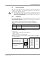
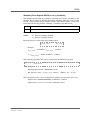
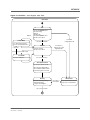
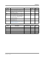
1.1
Maps of the Board
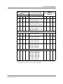
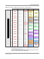
Figure 1. Map of the Board – front view
A14c Standard
Seond Front
COM20..23
(via 40-pin
connector)
Alternative
COM20..23
via 10-pin
connectors
L
L
A LAN1 L
A LAN1 L
COM20
A LAN2 L
A LAN2 L
A LAN3
A LAN3
COM21
COM1
COM1
COM22
COM23
PMC 1
COM23
COM22
COM21
PMC 0
COM20
MEN Mikro Elektronik GmbH
20A014-00 E2 – 2007-08-16
19
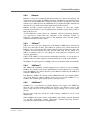
Getting Started
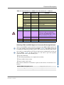
The A14C uses a plug-on module for CPU and I/O functionality. This plug-on board
also incorporates the SO-DIMM SDRAM.
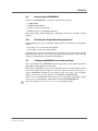
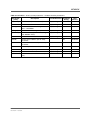
Figure 2. Map of the Board – top view
Reset button
LAN1
LAN3
VMEbus P1
Heat Sink
(facing in)
J2 — I/O
LAN2
J1 — PCI-104
MPC8540
Plug-on
Module
SO-DIMM
COM1
SA-Adapter
COM23
PMC1
SA-Adapter
COM22
VMEbus P2
SA-Adapter
COM21
PMC0
J4 rear I/O
Hard disk on adapter card
SA-Adapter
COM20
IDE
fuse
Quad UART COM 20..23
MEN Mikro Elektronik GmbH
20A014-00 E2 – 2007-08-16
IDE Interface
20
Getting Started
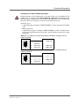
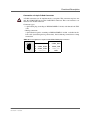
1.2
Configuring the Hardware
You should check your hardware requirements before installing the board in a
system, since most modifications are difficult or even impossible to do when the
board is mounted in a rack.
The following check list gives an overview on what you might want to configure.
; UART (COM20..23) extension through MEN standard SA-Adapters
The board provides one 40-pin I/O connector for connection of up to four
additional COM interfaces (COM20..23).
MEN provides a range of standard adapters and a mounting kit for four 9-pin
D-Sub connectors accessible through a second front panel.
Please see MEN’s website for ordering information.
Refer to Chapter 2.11 UART COM20..COM23 Interfaces on page 38.
; IDE devices
The board provides an IDE connector for hard disks or other IDE devices.
MEN also offers a suitable adapter cable for two devices.
Please see MEN’s website for ordering information.
Refer to Chapter 2.7 IDE Interface on page 28 for details on the IDE
interface.
; PMC modules
Refer to Chapter 2.13.1 Installing a PMC Mezzanine Module on page 47
for a detailed installation description.
MEN Mikro Elektronik GmbH
20A014-00 E2 – 2007-08-16
21
Getting Started
1.3
Integrating the Board into a System
You can use the following check list when installing the board in a system for the
first time and with minimum configuration.
!
The board is completely trimmed on delivery.
; Power-down the system.
; Remove all boards from the VMEbus system.
; Insert the A14C into slot 1 of the system, making sure that the VMEbus connectors are properly aligned.
; Connect a terminal to the RS232 interface COM1 (RJ45 connector).
(MEN offers an adapter cable with a standard 9-pin D-Sub plug connector.
Please see MEN’s website for ordering information.)
; Set your terminal to the following protocol:
-
9600 baud data transmission rate
8 data bits
1 stop bit
No parity
; Power-up the system.
; The terminal displays a message similar to the following:
___________________ Secondary MENMON for MEN EM3 Family 1.3 _________________
|
|
|
(c) 2005 - 2005 MEN Mikro Elektronik GmbH Nuremberg
|
|
MENMON 2nd Edition, Created Nov 18 2005
15:57:50
|
|_____________________________________________________________________________|
|
CPU Board: EM08-01
|
CPU: MPC8540
|
|Serial Number: 66
|
CPU/MEM Clk: 792 / 132 MHz
|
| HW Revision: 00.05.02
|CCB/BRG/LBC Clk: 264 /
0 / 33 MHz
|
|
|
PCI: 32 Bit / 33 MHz
|
|
DDR SDRAM: 512 MB ECC off 2.0/3/6|
FRAM:
32 kB
|
|
Produced:
|
FLASH:
8 MB
|
| Last repair:
|
Reset Cause: Button
|
|_____________________________________________________________________________|
| Carrier Board: A500c02, Rev 02.04.00, Serial 148
|
\___________________________________________________________________________/
Setting speed of NETIF 0 to AUTO
Setting speed of NETIF 1 to AUTO
Setting speed of NETIF 2 to AUTO
press 'ESC' for MENMON, 's' for setup
(Can't load BOOTLOGO.BMP)
Test SDRAM
: OK
Test ETHER0
: OK
Test ETHER1
: OK
Test FRAM
: OK
Test EEPROM
: OK
Test RTC
: OK
Test IDE0-NAND
: OK
Telnet daemon started on port 23
HTTP daemon started on port 80
MenMon>
MEN Mikro Elektronik GmbH
20A014-00 E2 – 2007-08-16
22
Getting Started
; Now you can use the MENMON BIOS/firmware (see detailed description in
Chapter 4 MENMON on page 93).
; Observe the installation instructions for the respective software.
1.4
Installing Operating System Software
The board supports VxWorks, Linux and QNX.
!
By standard, no operating system is installed on the board. Please refer to the
operating system installation documentation on how to install the software!
You can find any software available on MEN’s website.
MEN Mikro Elektronik GmbH
20A014-00 E2 – 2007-08-16
23
Functional Description
2
Functional Description
The following describes the individual functions of the board and their
configuration on the board. There is no detailed description of the individual
controller chips and the CPU. They can be obtained from the data sheets or data
books of the semiconductor manufacturer concerned (Chapter 6.1 Literature and
Web Resources on page 118).
2.1
Power Supply
The board is supplied with +5 V and ±12 V via the VMEbus. However, ±12 V may
be required only by some mezzanine modules. The plug-on CPU card itself is
supplied via PCI-104 connectors J1/J2.
The on-board power supply generates the 1.2 V core voltage for the CPU, 2.5 V for
memory and the 1.5 V core voltage for the FPGA.
2.1.1
Watchdog
A voltage monitor supervises 5 V, 3.3 V, 2.5 V and 1.2 V and holds the CPU in reset
condition until all supply voltages are within their nominal values. In addition this
device contains a watchdog that must be triggered. The watchdog timeout switches
automatically from 56 s after reset to 1.6 s after the first trigger pulse. This allows a
longer watchdog timeout period during the start-up phase.
After power-up the CPU loads the FPGA. The configuration file depends on the
application. After configuration the FPGA serves the external hardware watchdog
without further action by the CPU. If there is any problem loading the FPGA, the
external watchdog causes a reset.
An additional watchdog is implemented in the FPGA.
See also Chapter 4.6.6.5 Hardware Monitor Support – Parameter psrXXX on page
112.
2.2
Clock Supply
The CPU is supplied with one copy of the on-board PCI clocks. This is internally
multiplied to generate the core clock and the memory clock.
By default the A14C runs at 33 MHz (PCI), 132 MHz (SDRAM) and 792 MHz
(core).
2.3
Real-Time Clock
The board includes an RA8581 real-time clock. Interrupt generation of the RTC is
not supported. For data retention during power off the RTC is backed up by a
GoldCap capacitor. The GoldCap gives an autonomy of approx. two days when
fully loaded.
A control flag indicates a back-up power fail condition. In this case the contents of
the RTC cannot be expected to be valid. A message will be displayed on the
MENMON console in this case.
MEN Mikro Elektronik GmbH
20A014-00 E2 – 2007-08-16
24
Functional Description
2.4
PowerPC CPU
The board is equipped with the MPC8540 PowerQUICC III processor, which
includes a 32-bit PowerPC e500 core, the integrated host-to-PCI bridge, Ethernet
controllers and UARTs.
2.4.1
General
The PowerQUICC III is a versatile one-chip integrated microprocessor and
peripheral combination that can be used in a variety of controller applications,
excelling particularly in communications and networking products. The
PowerQUICC III provides high performance in all areas of device operation,
including great flexibility, extended capabilities, and high integration.
The PowerQUICC III architecture integrates two processing blocks. One block is a
high-performance embedded e500 core. With 256 KB of Level 2 cache, the e500
core implements the enhanced PowerPC Book E instruction-set architecture and
provides unprecedented levels of hardware and software debugging support. The
second block is the Communications Processor Module (CPM). The CPM of the
PowerQUICC III can support three fast serial communications controllers (FCCs),
two multichannel controllers (MCCs), four serial communications controllers
(SCCs), one serial peripheral interface (SPI), and one I2C interface.
The PowerQUICC III also offers two integrated 10/100/1000 Ethernet controllers, a
DDR SDRAM memory controller, and a 64-bit PCI controller. This high level of
integration helps simplify board design and offers significant bandwidth and
performance for high-end control-plane and data-plane applications.
2.4.2
Thermal Considerations
The CPU generates around 8 W of power dissipation when operated at 800 MHz.
To meet thermal requirements a suitable heat sink must be attached to the CPU and
sufficient airflow must be provided.
MEN provides a suitable heat sink to meet thermal requirements for the board.
!
Note: MEN gives no warranty on functionality and reliability of the A14C if you
use any other heat sink than that supplied by MEN. Please contact either
MEN directly or your local MEN sales office!
MEN Mikro Elektronik GmbH
20A014-00 E2 – 2007-08-16
25
Functional Description
2.5
Bus Structure
2.5.1
Host-to-PCI Bridge
The integrated host-to-PCI bridge is used as host bridge and memory controller for
the PowerPC processor. All transactions of the PowerPC to the PCI bus are
controlled by the host bridge. The FRAM and boot Flash are connected to the local
memory bus of the integrated host-to-PCI bridge.
The PCI interface is PCI bus Rev. 2.2 compliant and supports all bus commands and
transactions. Master and target operations are possible. Only big-endian operation is
supported.
2.5.2
Local PCI Bus
The local PCI bus is controlled by the integrated host-to-PCI bridge. It runs at
33 MHz. 64-bit/66-MHz PCI bus operation is available on request. In this case rows
C and D of board-to-board connector J2 are used for the 64-bit extension signals.
(See Chapter 2.14 Board-to-Board I/O Connector on page 48.)
The I/O voltage is fixed to 3.3V. The data width is 32 bits.
The FPGA is connected to the local PCI bus.
2.5.3
PCI-to-PCI Bridge
The A14C has a secondary PCI bus for accesses to PMC modules. It is controlled by
a PCI-to-PCI bridge of type PCI6154 from PLX.
2.5.4
PCI-to-VMEbus Bridge
The board has a PCI-to-VME bridge for connection to the VMEbus. It is
implemented in an additional FPGA. On the local PCI bus this bridge is a master.
The local processor can thus freely access the VMEbus (master). For
communication in multiprocess applications, the bridge has a fast communication
memory of 1 MB size. This memory can be accessed both from the local processor
and from the VMEbus (slave).
MEN Mikro Elektronik GmbH
20A014-00 E2 – 2007-08-16
26
Functional Description
2.6
Memory
The standard board versions provide a memory configuration suitable for many
applications. However, memory on the A14C can also be configured for your needs.
For standard memory sizes and ordering options please see MEN’s website.
2.6.1
DRAM System Memory
One DDR SDRAM bank (bank 0) is implemented on the board. Bank 0 is connected
to a 200-pin SO-DIMM connector. The current board version supports SO-DIMM
modules up to 2 GB. By standard, the SO-DIMM slot is populated with a suitable
module size.
!
Note: MEN gives no warranty on functionality and reliability of the board if you
use any other module than that qualified and/or supplied by MEN. Please
contact either MEN directly or your local MEN sales office.
2.6.2
Boot Flash
The board has on-board Flash. It is controlled by the CPU and can accommodate
8 MB. The data bus is 8 bits wide.
Flash memory contains the boot software for the MENMON/operating system
bootstrapper and application software. The MENMON sectors are softwareprotected against illegal write transactions through a password in the serial
download function of MENMON (cf. Chapter 4.4 Updating Boot Flash and NAND
Flash on page 97).
2.6.3
NAND Flash
The board includes up to 1 GB soldered NAND Flash memory controlled by the
FPGA. The data bus is 8 bits wide.
MEN's NAND-ATA controller provides wear leveling without user interaction.
Using the NAND-ATA controller the NAND Flash is seen as an ATA disk.
NAND Flash provides 100,000 erase cycles minimum and 10 years data retention.
See also Chapter 4.4 Updating Boot Flash and NAND Flash on page 97.
2.6.4
FRAM
The board has 32 KB non-volatile FRAM memory connected to the local bus of the
CPU.
The FRAM does not need a back-up voltage for data retention.
2.6.5
Additional SDRAM
By standard, the board is supplied with 16 MB additional SDRAM. It is controlled
by the FPGA and can be used for graphics or other functions.
2.6.6
EEPROM
The board has a 4-kbit serial EEPROM for factory data, MENMON parameters, and
for the VxWorks bootline.
MEN Mikro Elektronik GmbH
20A014-00 E2 – 2007-08-16
27
Functional Description
2.7
IDE Interface
The parallel IDE (PATA) interface handles the exchange of information between the
processor and peripheral devices such as hard disks, ATA CompactFlash cards and
CD-ROM drives.
The IDE interface is controlled by the FPGA and supports up to two ATA devices in
PIO mode 0. One device acts as a master, the other as a slave.
2.7.1
Connection
You can connect one or two devices to the standard 44-pin connector. MEN offers a
suitable adapter cable for two devices. For ordering options, please see MEN’s
website.
The 44-pin IDE connector is located at the top side of A14C. The pinning of the
IDE connector complies with the ATA-4/ATAPI specification.
Connector types:
• 44-pin, 2-row plug, 2mm pitch
• Mating connector:
44-pin, 2-row receptacle, 2mm pitch
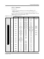
Table 1. Pin assignment of 44-pin IDE plug connector
1
43
MEN Mikro Elektronik GmbH
20A014-00 E2 – 2007-08-16
2
44
1
IDE_RST#
2
GND
3
IDE_D[7]
4
IDE_D[8]
5
IDE_D[6]
6
IDE_D[9]
7
IDE_D[5]
8
IDE_D[10]
9
IDE_D[4]
10
IDE_D[11]
11
IDE_D[3]
12
IDE_D[12]
13
IDE_D[2]
14
IDE_D[13]
15
IDE_D[1]
16
IDE_D[14]
17
IDE_D[0]
18
IDE_D[15]
19
GND
20
-
21
-
22
GND
23
IDE_WR#
24
GND
25
IDE_RD#
26
GND
27
IDE_RDY
28
-
29
-
30
GND
31
IDE_IRQ
32
-
33
IDE_A[1]
34
GND
35
IDE_A[0]
36
IDE_A[2]
37
IDE_CS1#
38
IDE_CS3#
39
-
40
GND
41
+5V
42
+5V
43
GND
44
GND
28
Functional Description
Table 2. Signal mnemonics of 44-pin IDE plug connector
Signal
Function
+5V
out
+5V power supply, current-limited to 3A by a fuse
GND
-
Digital ground
IDE_A[2:0]
out
IDE address [2:0]
IDE_CS1#
out
IDE chip select 1
IDE_CS3
out
IDE chip select 3
IDE_D[15:0]
in/out
IDE data [15:0]
IDE_IRQ
in
IDE interrupt request
IDE_RD#
out
IDE read strobe
IDE_RDY
in
IDE ready
IDE_RST#
out
IDE reset
IDE_WR#
out
IDE write strobe
2.7.1.1
!
Direction
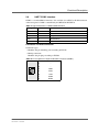
Fuse Protection
The IDE interface is protected by a fuse. This fuse is not intended to be exchanged
by the customer. Your warranty for the A14C will cease if you exchange the
fuse on your own. Please send your board to MEN for repair if the fuse blows.
•
•
•
•
Current rating: 3A
Type: fast
Size: 1206
MEN part number: 5675-0003
The fuse is located on the top side of A14C.
Figure 3. Position of fuse for IDE protection
VMEbus P2
SA-Adapter
COM21
J4 rear I/O
Hard disk on adapter card
SA-Adapter
COM20
IDE
fuse
Quad UART COM 20..23
MEN Mikro Elektronik GmbH
20A014-00 E2 – 2007-08-16
IDE Interface
29
Functional Description
2.7.2
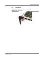
Installing a Hard Disk
A hard-disk adapter card for installation of a 2.5", 9.5-mm hard-disk drive is
available from MEN. The adapter is designed in such a way that standard hard disks
can easily be installed. For flexibility the adapter does not include the hard disk
itself but includes all necessary screws to mount a standard hard disk.
Please see MEN’s website for ordering options.
If you want to install a hard disk on the board using MEN’s adapter card, please
keep in mind that the assembly occupies the space usually used for PMC slot 0 or
for SA-Adapters on COM20 and COM21. See Figure 2, Map of the Board – top
view, on page 20.
The board needs only one slot in the system even with a hard disk installed. In this
case no component pins of neighboring boards may exceed the interboard
separation plane.
Perform the following steps to install a hard disk using MEN’s hard-disk
adapter card:
; Power-down your system and remove the A14C from the system.
; Remove the PMC module from slot 0 if installed.
; Plug the hard disk’s connector to the adapter card, carefully pushing the connectors together. Make sure to match the pins correctly.
; Fasten the hard disk to the adapter card at the bottom side of the adapter using
the four cross-recess screws (M3x5) and suitable nuts provided with the
adapter.
MEN Mikro Elektronik GmbH
20A014-00 E2 – 2007-08-16
30
Functional Description
; Plug the hard-disk adapter card to the 44-pin IDE connector on A14C.
; Fasten the hard-disk adapter card to A14C at the bottom side of the A14C using
the four recess screws (M2.5x4) and suitable nuts provided with the adapter.
; Reinsert the board into your system.
MEN Mikro Elektronik GmbH
20A014-00 E2 – 2007-08-16
31
Functional Description
2.8
Ethernet Interfaces
The A14C has three Ethernet interfaces controlled by the CPU. LAN3 supports
10 Mbits/s and 100 Mbits/s, and LAN1/LAN2 support up to 1000 Mbits/s. All
interfaces support full-duplex operation.
!
Note: The unique Ethernet address is set at the factory and should not be changed.
Any attempt to change this address may create node or bus contention and
thereby render the board inoperable. A label on the Ethernet connectors of the
board gives the set Ethernet address.
2.8.1
Connection
Three standard RJ45 connectors or two D-Sub connectors are available at the front
panel for connection to network environments. Two status LEDs for each connector
are accommodated at the front.
The pin assignments correspond to the Ethernet specification IEEE802.3.
Table 3. Signal mnemonics of Ethernet 10Base-T/100Base-TX/1000Base-TX
interfaces
Signal
Direction
Function
MDX[0:3]+/- in/out
Differential pairs of data lines for 1000Base-T
RX+/-
in
Differential pair of receive data lines for 10/100Base-T
TX+/-
out
Differential pair of transmit data lines for 10/100Base-T
Connection via RJ45 Connectors
Connector types:
• Modular 8/8-pin mounting jack according to FCC68
• Mating connector:
Modular 8/8-pin plug according to FCC68
Table 4. Pin assignment of 8-pin RJ45 Ethernet 10Base-T/100Base-TX/1000BaseTX connectors (LAN1..3)
1000Base-T 10/100Base-T
Lights up whenever there is
transmit or receive activity
A
1
Lights up as soon as the
link is established
L
8
1
MDX[0]+
TX+
2
MDX[0]-
TX-
3
MDX[1]+
RX+
4
MDX[2]+
-
5
MDX[2]-
-
6
MDX[1]-
RX-
7
MDX[3]+
-
8
MDX[3]-
-
Note: Please note that LAN3 supports only 10/100Base-T!
MEN Mikro Elektronik GmbH
20A014-00 E2 – 2007-08-16
32
Functional Description
Connection via 9-pin D-Sub Connectors
!
D-Sub connectors can be implemented as an option. In this case, only 10Base-T and
100Base-TX are supported, no Gigabit Ethernet connection. In addition, the DSub connector for LAN3 replaces not only the LAN3 RJ45 but also the COM1 RJ45
connector. These two interfaces are routed to one D-Sub connector.
Connector types:
• 9-pin D-Sub plug according to DIN41652/MIL-C-24308, with thread bolt UNC
4-40
• Mating connector:
9-pin D-Sub receptacle according to DIN41652/MIL-C-24308, available for ribbon cable (insulation piercing connection), hand-soldering connection or crimp
connection
Table 5. Pin assignment of 9-pin D-Sub 10Base-T/100Base-TX plug connector
(LAN1 and LAN2)
6
9
1
5
1
LAN1_TX+
6
LAN1_TX-
2
LAN2_TX+
7
LAN2_TX-
3
-
8
LAN2_RX-
4
LAN2_RX+
9
LAN1_RX-
5
LAN1_RX+
Table 6. Pin assignment of 9-pin D-Sub 10Base-T/100Base-TX plug connector
(LAN3 and COM1)
6
9
MEN Mikro Elektronik GmbH
20A014-00 E2 – 2007-08-16
1
5
1
LAN3_TX+
6
LAN3_TX-
2
COM1_RXD
7
COM1_RTS#
3
COM1_TXD
8
COM1_CTS#
4
LAN3_RX+
9
LAN3_RX-
5
GND
33
Functional Description
2.8.2
General
Ethernet is a local-area network (LAN) protocol that uses a bus or star topology and
supports data transfer rates of 100Mbps and more. The Ethernet specification served
as the basis for the IEEE 802.3 standard, which specifies the physical and lower
software layers. Ethernet uses the CSMA/CD access method to handle simultaneous
demands. It is one of the most widely implemented LAN standards.
Ethernet networks provide high-speed data exchange in areas that require
economical connection to a local communication medium carrying bursty traffic at
high-peak data rates.
A classic Ethernet system consists of a backbone cable and connecting hardware
(e.g. transceivers), which links the controllers of the individual stations via
transceiver (transmitter-receiver) cables to this backbone cable and thus permits
communication between the stations.
2.8.3
10Base-T
10Base-T is one of several adaptations of the Ethernet (IEEE 802.3) standard for
Local Area Networks (LANs). The 10Base-T standard (also called Twisted Pair
Ethernet) uses a twisted-pair cable with maximum lengths of 100 meters. The cable
is thinner and more flexible than the coaxial cable used for the 10Base-2 or
10Base-5 standards. Since it is also cheaper, it is the preferable solution for costsensitive applications.
Cables in the 10Base-T system connect with RJ45 connectors. A star topology is
common with 12 or more computers connected directly to a hub or concentrator.
The 10Base-T system operates at 10Mbps and uses baseband transmission methods.
2.8.4
100Base-T
The 100Base-T networking standard supports data transfer rates up to 100Mbps.
100Base-T is actually based on the older Ethernet standard. Because it is 10 times
faster than Ethernet, it is often referred to as Fast Ethernet. Officially, the 100Base-T
standard is IEEE 802.3u.
Like Ethernet, 100Base-T is based on the CSMA/CD LAN access method. There
are several different cabling schemes that can be used with 100Base-T, e.g.
100Base-TX, with two pairs of high-quality twisted-pair wires.
2.8.5
1000Base-T
1000Base-T is a specification for Gigabit Ethernet over copper wire (IEEE Std.
802.3ab). The standard defines 1Gbps data transfer over distances of up to 100
meters using four pairs of CAT-5 balanced copper cabling and a 5-level coding
scheme.
Because many companies already use CAT-5 cabling, 1000Base-T can be easily
implemented.
Other 1000Base-T benefits include compatibility with existing network protocols
(i.e. IP, IPX, AppleTalk), existing applications, Network Operating Systems,
network management platforms and applications.
MEN Mikro Elektronik GmbH
20A014-00 E2 – 2007-08-16
34
Functional Description
2.9
UART COM1 Interface
COM1 is a standard RS232 interface. It is available via an RJ45 or D-Sub connector
at the front panel. COM1 is controlled by the MPC8540 DUART 0.
Table 7. Signal mnemonics of UART COM1 interface
Signal
Direction
Function
CTS#
in
Clear to send
GND
-
Ground
RTS#
out
Request to send
RXD
in
Receive data
TXD
out
Transmit data
Connection via RJ45 Connector
Connector types:
• Modular 8/8-pin mounting jack according to FCC68
• Mating connector:
Modular 8/8-pin plug according to FCC68
Table 8. Pin assignment of 8-pin RJ45 UART connector (COM1)
1
1
-
2
-
3
-
4
GND
5
RXD
6
TXD
7
CTS#
8
RTS#
8
MEN Mikro Elektronik GmbH
20A014-00 E2 – 2007-08-16
35
Functional Description
Connection via 9-pin D-Sub Connector
!
A D-Sub connector can be implemented as an option. This connector replaces not
only the COM1 RJ45 but also the LAN3 RJ45 connector. These two interfaces are
routed to one D-Sub connector.
Connector types:
• 9-pin D-Sub plug according to DIN41652/MIL-C-24308, with thread bolt UNC
4-40
• Mating connector:
9-pin D-Sub receptacle according to DIN41652/MIL-C-24308, available for ribbon cable (insulation piercing connection), hand-soldering connection or crimp
connection
Table 9. Pin assignment of 9-pin D-Sub COM1/LAN3 plug connector
6
9
MEN Mikro Elektronik GmbH
20A014-00 E2 – 2007-08-16
1
5
1
LAN3_TX+
6
LAN3_TX-
2
COM1_RXD
7
COM1_RTS#
3
COM1_TXD
8
COM1_CTS#
4
LAN3_RX+
9
LAN3_RX-
5
GND
36
Functional Description
2.10
UART COM10 Interface
The A14C provides an additional, LVTTL-level, UART interface controlled by the
FPGA accessible via rear I/O on connector P2.
The UART port is compatible with MEN’s SA-Adapter standard, which offers a
selection of different physical interfaces from RS232 to RS485. You can use SAAdapters on a suitable transition module. Please contact MEN’s sales team if you
have special needs.
For the pin assignment please see Table 30, Pin assignment of VMEbus rear I/O
connector P2 – FPGA I/O signals, on page 80.
!
Please note that PMC I/O signals are directly connected to connector P2. If you
use COM10 I/O signals via P2, you must make sure that these signals do not
interfere with PMC I/O signals, since this may cause damage to the CPU
board. See Chapter 2.16.16.1 Rear I/O using VMEbus P2 on page 77 for more
details and for pin assignments of P2.
MEN Mikro Elektronik GmbH
20A014-00 E2 – 2007-08-16
37
Functional Description
2.11
UART COM20..COM23 Interfaces
The A14C provides a quad UART for standard serial ports COM20..COM23. The
LVTTL-level UARTs are controlled by the on-board OX16PCI954 controller. It
supports the following baud rates: 1200, 2400, 4800, 9600, 19200, 38400, 57600,
115200.
The UART signals are available
• either via a 40-pin plug connector, which is available on all versions of A14C,
• or directly via four 10-pin SA-Adapter connectors at the front of the board.
The on-board 10-pin SA-Adapter connectors at the front are an option and are only
available on request. If all of those SA-Adapter ports are implemented on A14C,
you cannot use any PMC slots. Also, COM20 and COM21 would collide with the
hard disk adapter.
Please ask our sales team for more information and for customized versions of
A14C!
You can find more information on MEN SA-Adapters on MEN’s website.
Table 10. Signal mnemonics for UART COM20..COM23 interfaces
Signal
Function
+5V
-
+5V power supply; current-limited to 1.5A by a fuse
with 10-pin connectors
CTS#
in
Clear to send
DCD#
in
Data carrier detect
DSR#
in
Data set ready
DTR#
out
Data terminal ready
GND
-
Digital ground
RI#
in
Ring indicator
RTS#
out
Request to send
RXD
in
Receive data
TXD
out
Transmit data
MEN Mikro Elektronik GmbH
20A014-00 E2 – 2007-08-16
Direction
38
Functional Description
2.11.1
Connection via 40-pin Connector
You can use the on-board 40-pin plug connector with SA-Adapters using ribbon
cabling. A suitable mounting kit for easy connection of four SA-Adapters using an
additional front panel is available from MEN. (See also Figure 1, Map of the Board
– front view, on page 19.)
Connector types:
• 40-pin low-profile plug, 2.54mm pitch, for ribbon-cable connection
• Mating connector:
40-pin IDC receptacle, e.g. Elco Series 8290 IDC socket
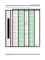
Table 11. Pin assignment of the 40-pin UART COM20..COM23 connector
1
39
MEN Mikro Elektronik GmbH
20A014-00 E2 – 2007-08-16
2
40
1
GND
2
+5V
3
TXD23
4
RXD23
5
DTR23#
6
RTS23#
7
DSR23#
8
CTS23#
9
DCD23#
10
RI23#
11
GND
12
+5V
13
TXD22
14
RXD22
15
DTR22#
16
RTS22#
17
DSR22#
18
CTS22#
19
DCD22#
20
RI22#
21
GND
22
+5V
23
TXD21
24
RXD21
25
DTR21#
26
RTS21#
27
DSR21#
28
CTS21#
29
DCD21#
30
RI21#
31
GND
32
+5V
33
TXD20
34
RXD20
35
DTR20#
36
RTS20#
37
DSR20#
38
CTS20#
39
DCD20#
40
RI20#
COM23
COM22
COM21
COM20
39
Functional Description
2.11.1.1 Installing Standard SA-Adapters using the On-board
40-pin Connector
MEN offers a special mounting kit for easy installation of SA-Adapters. It includes
an additional front panel for four SA-Adapters and a suitable ribbon cable leading to
four 10-pin connectors. Please refer to MEN’s website for ordering information.
!
Note: MEN gives no warranty on functionality and reliability of the board and SAAdapters used if you install SA-Adapters in a different way than described in
MEN’s documentation.
Perform the following steps to install standard SA-Adapters using MEN’s SAAdapter mounting kit:
; Power-down your system and remove the A14C from the system.
; Plug the 40-pin prefolded ribbon cable to the 40-pin UART connector on A14C.
Make sure to align the pins correctly.
Please note that the ribbon cable also fits when PMC modules are installed, as
is shown in the photo above.
; Remove the two front panel screws and the two screws on top of the mounting
bolts of the SA-Adapter.
; Remove the blind connector from the additional front panel, if you need a slot
that is covered: Loosen the two screws at the front of the panel.
COM20
MEN Mikro Elektronik GmbH
20A014-00 E2 – 2007-08-16
COM21
COM22
COM23
40
Functional Description
; Plug the suitable 10-pin connector of the ribbon cable to the respective 10-pin
SA-Adapter connector.
Make sure to always align the pins correctly (pin 1 is marked by a triangle on
the ribbon cable connector).
; Use the SA-Adapter’s front panel screws to fasten the adapter at the additional
front panel.
; You can now reinsert the board and the additional front panel into your system.
Make sure to fasten the SA-Adapter front panel appropriately in your enclosure!
MEN Mikro Elektronik GmbH
20A014-00 E2 – 2007-08-16
41
Functional Description
2.11.2
Connection via 10-pin SA-Adapter Connectors
Four 10-pin connectors can be assembled that allow direct connection to MEN SAAdapters. See Figure 2, Map of the Board – top view, on page 20.
Connector types:
• 10-pin IDC receptacle, 2.54mm pitch, for ribbon-cable connection
• Mating connector:
10-pin low-profile plug
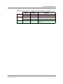
Table 12. Pin assignment of the 10-pin UART COM20..COM23 connectors
9
1
10
2
9
DCD#
10
RI#
7
DSR#
8
CTS#
5
DTR#
6
RTS#
3
TXD
4
RXD
1
GND
2
+5V
2.11.2.1 Installing SA-Adapters Directly on A14C
With 10-pin connectors, you can install SA-Adapters directly on the A14C, like a
mezzanine module, with the I/O connector at the front.
Note: Please note that you can install adapters on the A14C directly only if you
have a suitable version of A14C (without PMC slots)!
Perform the following steps to install an SA-Adapter:
; Make sure that the adapter matches the standard dimensions for SA-Adapters.
(See also installation hints in the adapter’s user manual.)
; Power down your system and remove the A14C from the system.
; Remove the two front panel screws and the two screws on top of the mounting
bolts of the SA-Adapter.
; Remove the blind connector from the front panel, if you need a slot that is covered: Loosen the two screws at the front of the panel.
COM23
COM22
COM21
COM20
; The SA-Adapter is plugged on the A14C with the component sides of the PCBs
facing each other.
MEN Mikro Elektronik GmbH
20A014-00 E2 – 2007-08-16
42
Functional Description
; Put the SA-Adapter’s front connector through the A14C’s front slot at a 45°
angle.
; Carefully put it down, making sure that the connectors are properly aligned.
; Press the SA-Adapter firmly onto the A14C.
; Screw the SA-Adapter tightly to the A14C using the front-panel and standoff
screws removed before.
Figure 4. Installing SA-Adapters on A14C directly
SA-Adapter
Mounting
standoff
10-pin connectors
CPU board
2 M3x6 pan-head
screws according to
DIN85 with washers
MEN Mikro Elektronik GmbH
20A014-00 E2 – 2007-08-16
43
Functional Description
2.11.2.2 Fuse Protection
!
The 10-pin COM20..COM23 interfaces are protected by one fuse each. These fuses
are not intended to be exchanged by the customer. Your warranty for the A14C
will cease if you exchange the fuses on your own. Please send your board to MEN
for repair if a fuse blows.
•
•
•
•
Current rating: 1.5A
Type: fast
Size: 1206
MEN part number: 5675-0001
The fuses are located on the bottom side of A14C.
Figure 5. Position of fuse for COM20..COM23 protection
COM23 fuse
COM22 fuse
COM21 fuse
COM20 fuse
MEN Mikro Elektronik GmbH
20A014-00 E2 – 2007-08-16
44
Functional Description
2.12
GPIO
Five GPIO controllers are included in the FPGA. Each of them controls eight I/O
signals, totalling 40 signals. One of these signals is fixed to a specific function:
GPIO2.4 is used as push-button reset input. This leaves 39 completely userdefinable lines.
All pins are directly connected to the FPGA. Voltage levels are LVTTL.
You can control the GPIO lines through software using MDIS4 driver software
available on MEN’s website. The following table gives the assignment of the GPIO
controllers implemented in the A14C’s FPGA to their function on the board.
Normally you can identify the controllers by their instance numbers in your
operating system.
Table 13. Assignment of 16Z034_GPIO controllers
Instance
Function
0
GPIO lines 0.0 to 0.7 (bits 0..7)
1
GPIO lines 1.0 to 1.7 (bits 0..7)
2
GPIO lines 2.0 to 2.7 (bits 0..7)
GPIO2.4 is used for push button reset
3
GPIO lines 3.0 to 3.7 (bits 0..7)
4
GPIO lines 4.0 to 4.7 (bits 0..7)
The GPIO signals are available via rear I/O on connector P2. For the pin assignment
please see Table 30, Pin assignment of VMEbus rear I/O connector P2 – FPGA I/O
signals, on page 80.
Since all of the GPIO signals are controlled by the FPGA, you could also use the
respective pins on P2 to implement other rear I/O functions in FPGA instead of
GPIO. Please contact MEN’s sales team if you have special needs.
!
Please note that PMC I/O signals are directly connected to connector P2. If you
use GPIO I/O signals via P2, you must make sure that these signals do not
interfere with PMC I/O signals, since this may cause damage to the CPU
board. See Chapter 2.16.16.1 Rear I/O using VMEbus P2 on page 77 for more
details and for pin assignments of P2.
MEN Mikro Elektronik GmbH
20A014-00 E2 – 2007-08-16
45
Functional Description
2.13
PMC Slots
The A14C board provides two PMC slots for extension such as graphics, Fast
Ethernet etc. The market offers lots of different PMC mezzanines.
!
The signaling voltage is set to 3.3 V, i. e. the CPU board has no voltage key (see
Figure 6, Installing a PMC mezzanine module, on page 47) and can only carry PMC
mezzanines that support this keying configuration. Mezzanine cards may be
designed to accept either or both signaling voltages (3.3 V / 5 V).
The PMC slots support 32-bit and 64-bit PCI bus operation at 33 MHz or 66 MHz.
The connector layout is fully compatible to the IEEE1386 specification. For
connector pinouts please refer to the specification (see Chapter 6.1 Literature and
Web Resources on page 118).
PMC slot 0 supports rear I/O connection. PMC slot 1 does not support rear I/O! (See
also Figure 2, Map of the Board – top view, on page 20.)
!
Please note that PMC I/O signals are directly connected to connector P2. If you
use FPGA I/O signals (e.g. COM10, GPIO) via P2, you must make sure that
these signals do not interfere with PMC I/O signals, since this may cause
damage to the CPU board. See Chapter 2.16.16.1 Rear I/O using VMEbus P2 on
page 77 for more details and for pin assignments of P2.
Connector types:
• 64-pin, 1-mm pitch board-to-board receptacle according to IEEE 1386
• Mating connector:
64-pin, 1-mm pitch board-to-board plug according to IEEE 1386
MEN Mikro Elektronik GmbH
20A014-00 E2 – 2007-08-16
46
Functional Description
2.13.1
Installing a PMC Mezzanine Module
Perform the following steps to install a PMC module:
; Make sure that the voltage keying of your PMC module matches the A14C.
; Power down your system and remove the A14C from the system.
; Remove the filler panel from the board’s front PMC slot, if installed.
; The PMC module is plugged on the A14C with the component sides of the
PCBs facing each other.
; Put the PMC module’s front connector through the A14C’s front slot at a 45°
angle.
; Carefully put it down, making sure that the connectors are properly aligned.
; Press the PMC module firmly onto the A14C.
; Make sure that the EMC gasket around the PMC front panel is properly in its
place.
; Screw the PMC module tightly to the A14C using the four mounting standoffs
and four matching oval-head cross-recessed screws of type M2.5x6.
Figure 6. Installing a PMC mezzanine module
PMC module
Mounting
standoff
64-pin connectors
CPU board
2 M2.5x6 ovalhead crossrecessed screws
MEN Mikro Elektronik GmbH
20A014-00 E2 – 2007-08-16
2 M2.5x6 oval-head
cross-recessed
screws
47
Functional Description
2.14
Board-to-Board I/O Connector
The board features a 120-pin PCI-104-standard connector which connects the plugon module (CPU) with the carrier card and thus leads all important I/O signals to
peripheral connectors. The type of I/O depends on the FPGA configuration of the
A14C, which is very flexible and can contain a number of FPGA IP cores. For more
information on the FPGA, please refer to Chapter 3 FPGA on page 82.
This manual describes the standard factory FPGA configuration that is used on
model 01A014C00. (See also Chapter 3.3 Standard Factory FPGA Configuration on
page 92.) This version of the A14C provides the following interfaces:
•
•
•
•
!
IDE
UART COM10
GPIO (40 lines)
Miscellaneous functions
You can use FPGA signals also via rear I/O on VME connector P2. Please note that
PMC I/O signals are directly connected to connector P2. If you use FPGA I/O
signals (e.g. COM10, GPIO) via P2, you must make sure that these signals do
not interfere with PMC I/O signals, since this may cause damage to the CPU
board. See Chapter 2.16.16.1 Rear I/O using VMEbus P2 on page 77 for more
details and for pin assignments of P2.
Connector types:
• 4-row, 120-pin PCI-104 receptacle connector, 2mm pitch
• Mating connector:
4-row, 120-pin PCI-104 plug connector, 2mm pitch
MEN Mikro Elektronik GmbH
20A014-00 E2 – 2007-08-16
48
Functional Description
Table 14. Pin assignment of I/O connector J2 – factory standard FPGA
configuration
A B C D
1
2
30
MEN Mikro Elektronik GmbH
20A014-00 E2 – 2007-08-16
A
B
C
D
1
IDE_RST#
GPIO_3.0
+5V
RXD10#
2
GND
GPIO_3.1
TXD10
+5V
3
IDE_D7
GND
DTR10#
RTS10#
4
IDE_D6
IDE_D8
GND
CTS10#
5
+3.3V
IDE_D9
DSR10#
GND
6
IDE_D5
+3.3V
DCD10#
RI10
7
IDE_D4
IDE_D10
+3.3V
GPIO_0.1
8
GND
IDE_D11
GPIO_0.0
+3.3V
9
IDE_D3
GND
GPIO_0.2
GPIO_0.3
10
IDE_D2
IDE_D12
GND
GPIO_0.5
11
+5V
IDE_D13
GPIO_0.4
GND
12
IDE_D1
+5V
GPIO_0.6
GPIO_0.7
13
IDE_D0
IDE_D14
+5V
GPIO_1.1
14
GND
IDE_D15
GPIO_1.0
+5V
15
-
GND
GPIO_1.2
GPIO_1.3
16
IDE_WR#
GPIO_3.2
GND
GPIO_1.5
17
+3.3V
GPIO_3.3
GPIO_1.4
GND
18
IDE_RD#
+3.3V
GPIO_1.6
GPIO_1.7
19
IDE_RDY
-
+3.3V
GPIO_2.1
20
GND
GPIO_3.4
GPIO_2.0
+3.3V
21
-
GND
GPIO_2.2
GPIO_2.3
22
IDE_IRQ
GPIO_3.5
GND
GPIO_2.5
23
+5V
-
PBRST#
(GPIO_2.4)
GND
24
IDE_A1
+5V
GPIO_2.6
GPIO_2.7
25
IDE_A0
GPIO_3.6
+5V
GPIO_4.1
26
GND
IDE_A2
GPIO_4.0
+5V
27
IDE_CS1#
GND
GPIO_4.2
GPIO_4.3
28
GPIO_3.7
IDE_CS3#
GND
GPIO_4.5
29
+5V
SDA
GPIO_4.4
GND
30
SCL
+3.3V_STBY
GPIO_4.6
GPIO_4.7
49
Functional Description
Table 15. Signal mnemonics of I/O connector J2 – factory standard FPGA configuration
Signal
Power
Direction
Function
+3.3V
-
+3.3V power supply
+3.3V_STBY
in
Power supply for real-time clock and SRAM
+5V
-
+5V power supply
GND
-
Digital ground of respective interface
I²C
EEPROM
SCL
out
I²C bus
SDA
in/out
I²C bus
IDE
IDE_A[2:0]
out
IDE address [2:0]
IDE_CS1#
out
IDE chip select 1
IDE_CS3#
out
IDE chip select 3
IDE_D[15:0]
in/out
IDE data [15:0]
IDE_IRQ
in
IDE interrupt request
IDE_RD#
out
IDE read strobe
IDE_RDY
in
IDE ready
IDE_RST#
out
IDE reset
IDE_WR#
out
IDE write strobe
COM10_SW
out
COM10 mode
UARTs
0 = COM10 operates in RS422/485 mode
1 = COM10 operates in RS232 mode
Other
CTS10#
in
COM10 clear to send
DCD10#
in
COM10 Data carrier detect
DSR10#
in
COM10 Data set ready
DTR10#
out
COM10 Data terminal ready
RI10
in
COM10 Ring indicator
RTS10#
out
COM10 request to send
RXD10
in
COM10 receive data
TXD10
out
COM10 transmit data
GPIO_x
in/out
GPIO lines
PBRST#
in
Push button reset
MEN Mikro Elektronik GmbH
20A014-00 E2 – 2007-08-16
50
Functional Description
2.15
Reset Button
A reset button is integrated in the A14C’s front panel handle.
Figure 7. Position of reset button
Reset button
MEN Mikro Elektronik GmbH
20A014-00 E2 – 2007-08-16
51
Functional Description
2.16
VMEbus Interface
The A14C's VMEbus interface conforms to the VMEbus specification. It has the
following features:
• Slot-1 functionality with auto-detection
• Wide range of VMEbus address and data transfer modes
- Master D08(EO):D16:D32:D64:A16:A24:A32:ADO:BLT:RMW
- Slave D08(EO):D16:D32:D64:A16:A24:A32:BLT:RMW
• Interrupt handler: 7-level, D08(O):IH(7-1)
• Interrupter: 7-level, D08(O):I(7-1):ROAK
• Single level 3 fair requester
• Single level 3 arbiter
• BTO bus timeout
• DMA controller with scatter gather DMA (A32/D64)
• Mailbox functionality
• Location monitor A16, A24, A32
• Dual-ported system register
• Access to 1 MB dual-ported fast SRAM, 66-MHz or access to PCI space
MEN Mikro Elektronik GmbH
20A014-00 E2 – 2007-08-16
52
Functional Description
2.16.1
PCI Configuration Space Registers
The Configuration Registers from 0x00 to 0x3C conform with the PCI Device
Configuration Header Format.
Table 16. VMEbus interface PCI configuration space registers
Byte
Address
2
1
0
0x00
Device ID (0x5056)
Vendor ID (0x1172)
0x04
Status Register
Command Register
0x08
Class Code (0x068000)
0x0C
BIST
0x10
Base Address Register 0
0x14
Base Address Register 1
0x18
Base Address Register 2
0x1C
Base Address Register 3
0x20
Base Address Register 4
0x24
This register is always 0.
0x28
Card Bus CIS Pointer
0x2C
Subsystem ID (0x7A30)
0x30
Expansion ROM Base Address Register
0x34
Reserved
0x38
Reserved
0x3C
Maximum
Latency
MEN Mikro Elektronik GmbH
20A014-00 E2 – 2007-08-16
3
Header Type
Revision ID
(currently
0x01)
Latency Timer
Cache Line
Size
Subsystem Vendor ID (0x3032)
Minimum Grant Interrupt Pin
Interrupt Line
53
Functional Description
2.16.2
Runtime Registers
The registers are accessible both from the PCI and the VMEbus side.
From the PCI-bus side the address is the value of BAR 0 (e.g. 0x 8800 0000) plus
an offset (0x 0180 0000) plus the register address (e.g. 0x 0008 for ISTAT).
From the VMEbus side, the registers are accessible in A16 mode only. (E.g. slave
base address A16 = 0x00001000, plus register address).
Table 17. VMEbus runtime registers
Address
D31..D0
0x 0000
INTR – VME Interrupt Control Register (r/w)
0x 0004
INTID – VME Interrupt STATUS/ID Register (r/w)
0x 0008
ISTAT – Interrupt Status Register (r)
0x 000C
IMASK – Interrupt Mask Register (r/w)
0x 0010
MSTR – Master Control Register (r/w)
0x 0014
SLV24 – Slave Control Register A24 (r/w)
0x 0018
SYSCTL – System Controller Register (r/w)
0x 001C
LONGADD – Upper 3 Address Bits for A32 (r/w)
0x 0020
MAIL_IRQE – Mailbox Interrupt Enable Register (r/w)
0x 0024
MAIL_IRQ – Mailbox Interrupt Request Register (r/w)
0x 0028
PCI_OFFSET – PCI Offset Address (r/w)
0x 002C
DMASTA – DMA Status Register (r/w)
0x 0030
SLV16 – Slave Control Register A16 (r/w)
0x 0034
SLV32 – Slave Control Register A32 (r/w)
0x 0038
LOCSTA_0 – Location Status Register (r/w)
0x 003C
LOCSTA_1 – Location Status Register (r/w)
0x 0040
LOCADDR_0 – Location Monitor Address Register (r/w)
0x 0044
LOCADDR_1 – Location Monitor Address Register (r/w)
0x 0048
SLV24_PCI – A24 Slave Base Address for PCI (r/w)
0x 004C
SLV32_PCI – A32 Slave Base Address for PCI (r/w)
0x FF800
MAILBOX_0 – Mailbox Data Register (r/w)
0x FF804
MAILBOX_1 – Mailbox Data Register (r/w)
0x FF808
MAILBOX_2 – Mailbox Data Register (r/w)
0x FF80C
MAILBOX_3 – Mailbox Data Register (r/w)
0x FF900..FF90C
DMA_BD#1 – DMA Buffer Descriptor (r/w)
0x FF910..FF91C
DMA_BD#2 – DMA Buffer Descriptor (r/w)
.. 0x 0FF0..0FFC Further Buffer Descriptors
MEN Mikro Elektronik GmbH
20A014-00 E2 – 2007-08-16
54
Functional Description
2.16.3
VMEbus Master Mapping
The PCI to VMEbus bridge uses BAR0 to access the VMEbus. BAR1 is used for
VME A32/D32 accesses. BAR2 and BAR3 are equal to BAR0 and BAR1, but every
VMEbus access is swapped. BAR4 contains swapped and non-swapped A24/D32
windows.
Table 18. VMEbus interface BAR 0
BAR0
Size
Function
0x 0000 0000 .. 0x 00FF FFFC 16MB
VME A24 D16 (standard)
space
0x 0100 0000 .. 0x 0100 FFFC 64KB
VME A16 D16 (short) space
0x 0101 0000 .. 0x 0101 FFFC 64KB
VME A16 D32 (short) space
0x 0140 0000 .. 0x 014F FFFC 1MB
Local SRAM
0x 0180 0000 .. 0x 0180 0044 72 bytes
VME Bridge Control Registers
0x 01C0 0000
VME IACK space
16 bytes
Table 19. VMEbus interface BAR1
BAR1
Size
0x 0000 0000 .. 0x 1FFF FFFC 512MB
Function
VME A32 D32 (long) space
Table 20. VMEbus interface BAR2
BAR2
Size
Function
0x 0000 0000 .. 0x 00FF FFFC 16MB
VME A24 D16 (standard)
space swapped
0x 0100 0000 .. 0x 0100 FFFC 64KB
VME A16 D16 (short) space
swapped
0x 0101 0000 .. 0x 0101 FFFC 64KB
VME A16 D32 (short) space
swapped
0x 0140 0000 .. 0x 014F FFFC 1MB
Local SRAM
0x 0180 0000 .. 0x 0180 0044 72 bytes
VME Bridge Control Registers
Table 21. VMEbus interface BAR3
BAR3
Size
0x 0000 0000 .. 0x 1FFF FFFC 512MB
Function
VME A32 D32 (long) space
swapped
Table 22. VMEbus interface BAR4
BAR4
Function
0x 0000 0000 .. 0x 00FF FFFC 16MB
VME A24 D32 (standard)
space
0x 0100 0000 .. 0x 01FF FFFC 16MB
VME A24 D32 (standard)
space swapped
MEN Mikro Elektronik GmbH
20A014-00 E2 – 2007-08-16
Size
55
Functional Description
2.16.4
VME Slave Mapping
The PCI space, 1 MB SRAM, the internal RAM and all registers are accessible by
the VMEbus. The registers and the internal RAM is a 4-kB block, which is
accessible in A16 mode only. This block is mapped to the slave base address for
A16 mode. The SRAM can be mapped to the A24 and A32 base address, whereas
the SRAM is mirrored in A32 mode. The PCI space is also mapped to the A24 and
A32 space. The size of the A24/A32 windows is configurable in the corresponding
Mask Registers.
Table 23. VMEbus slave address windows
VME Slave
Access
Size
Address
Function
A16
72 bytes 0x 000 .. 0x 050
A24
64KB..
1MB
0x 0 0000 ..
0x F FFFC
Local SRAM
64KB..
1MB
0x 0 0000 ..
0x F FFFC
PCI Space
1MB
0x 0000 0000 ..
0x 000F FFFC
Local SRAM
1MB..
256MB
0x 0000 0000 ..
0x 000F FFFC
PCI Space
A32
2.16.5
VME Bridge Control Registers
SRAM
The SRAM is accessible from the PCI and VMEbus side. From the VMEbus side,
the base address is defined in the Slave Control Registers for A24 or A32 (in A32
mode the SRAM is mirrored!).
The SRAM has a size of 1 MB. It is accessible via block and standard transfers (user
and supervisor space).
MEN Mikro Elektronik GmbH
20A014-00 E2 – 2007-08-16
56
Functional Description
2.16.6
Slot-1 Function
The slot-1 function is auto-detected. It can be read from the SYSCTL register (bit
SYSCON). The A14C samples BG3IN# after SYSRES# has gone high. As specified
in the VMEbus specification all BG lines should be high after reset. Therefore only
in slot 1 /BG3IN can be sampled low, due to a local pull-down resistor.
After slot 1 is detected the functions listed below are enabled.
•
•
•
•
•
Generation of SYSRES#
Generation of SYSCLK (not provided during slot 1 detection cycle)
Level 3 arbitration
Bus arbitration timeout 250 µs
Bus transfer timeout 125 µs
The timeouts cannot be changed.
SYSCTL – System Controller Register (0x0018) (read/write)
ATO
SYSRES
SYSCON
MEN Mikro Elektronik GmbH
20A014-00 E2 – 2007-08-16
7..3
2
1
0
-
ATO
SYSRES
SYSCON
Monitor for arbitration timeout signal (read only)
0 = No arbitration timeout (default)
1 = Arbitration timeout occurred
Reset VMEbus; generates SYSRES# on the VMEbus
0 = SYSRES# not active
1 = SYSRES# active
System controller status (depends on slot 1 auto-detection after reset).
May be overridden by software.
0 = Slot 1 function disabled
1 = Slot 1 function enabled
57
Functional Description
2.16.7
VMEbus Master Interface
The A14C VMEbus master interface converts PCI bus cycles to VMEbus cycles.
The read/write cycles are performed in the A16, A24 and A32 address ranges of the
VMEbus. D08(E/O), D16 and D32 transfers will be executed. D64 transfers are
only possible with the DMA controller. The MSTR – Master Control Register
(0x0010) (read/write) enables the A14C to generate single RMW transfers or
Address-Only cycles.
MSTR – Master Control Register (0x0010) (read/write)
7..6
5
-
AONLY
AONLY
POSTWR
IBERREN
BERR
REQ
RMW
4
3
POSTWR IBERREN
2
1
0
BERR
REQ
RMW
Enable single address only cycle
0 = Normal cycle (default)
1 = Adress only cycle
The master does not transfer data with this cycle. Other slaves can
detect this cycle to generate local interrupts.
Only 8-bit or 16-bit read cycles are allowed for address-only cycles!
This bit will be reset after the transmission was done.
Posted Write Access to VMEbus (not supported)
0 = Delayed write access to VMEbus (default)
1 = Posted write access to VMEbus
Interrupt Bus Error Enable
0 = Local interrupt disabled if VMEbus bus error occurs (default)
1 = Local interrupt enabled if VMEbus bus error occurs
Monitor for VMEbus BERR# signal
0 = No VMEbus error (default)
1 = VMEbus error occurred; BERR# signal asserted. Cleared by
writing 1.
Set VMEbus requester scheme
0 = Request scheme for VMEbus master and interrupt handler is set to
Release On Request (ROR) (default)
1 = Request scheme is set to Release When Done (RWD)
If this bit is changed from 0 to 1, i. e. from ROR to RWD, and there
were previous accesses over the master interface, it is recommended to
do a dummy read to free the bus.
Enable single Read-Modifiy-Write cycle
0 = Normal cycle (default)
1 = RMW cycle. Master keeps AS# asserted during back-to-back read/
write cycle.
This bit is automatically cleared after the RMW cycle and must be set
for the next RMW cycle again.
The following master/slave RMW accesses are allowed:
• Byte or word access in D16 mode
• Byte, word or long access in D32 mode
Note: During RMW cycles all interrupts on the host CPU should be masked.
MEN Mikro Elektronik GmbH
20A014-00 E2 – 2007-08-16
58
Functional Description
In order to do a RMW cycle, the right order must be considered: First set the RMW
bit in the MSTR register. Now, a read transaction on VMEbus can be done (no long
access on D16 spaces!). When the read was done, the bus is blocked until the write
access will be performed. In order not to interfere with the RMW order, all other
VME master actions should be blocked by software (DMA should not be active!).
Transfers in D32 mode are done within one VME cycle. If a long access is
performed to a D16 address space, the VMEbus master will do two word accesses in
order to transmit 32 bits. These two accesses are not dividable by other VME
masters!
The following table lists all valid combinations for byte enables supported by the
bridge. Note that even within a PCI burst transfer the byte enables may change from
one data portion to the next. This must be taken into account when exchanging data
with the SRAM.
Table 24. VMEbus interface valid combinations for byte enables supported by PCIto-VME bridge
PCI Bus
(always dword aligned
address1)
Byte Lane Mapping
32-bit PCI 64-bit VME
Byte Enables
3
2
1
0
VMEbus
(always word aligned
address)
DS1 DS0
A1
LW
D16
1
1
1
1
No transfers
x
x
x
x
1
1
1
0
D7..D0 Ù D15..D8
0
1
0
1
1
1
0
1
D15..D8 Ù D7..D0
1
0
0
1
1
0
1
1
D23..D16 Ù D15..D8
0
1
1
1
0
1
1
1
D31..D24 Ù D7..D0
1
0
1
1
1
1
0
0
D7..D0 Ù D15..D8
D15..D8 Ù D7..D0
0
0
0
1
0
0
1
1
D23..D16 Ù D15..D8
D31..D24 Ù D7..D0
0
0
1
1
1
0
1
0
First: D23..D16 Ù D15..D8
Second: D7..D0 Ù D15..D8
0
0
1
1
1
0
1
0
1
0
1
First: D31..D24 Ù D7..D0
Second: D15..D8 Ù D7..D0
1
1
0
0
1
0
1
0
1
1
0
First: D31..D24 Ù D7..D0
Second: D7..D0 Ù D15..D8
1
0
0
1
1
0
1
1
0
0
1
First: D23..D16 Ù D15..D8
Second: D15..D8 Ù D7..D0
0
1
1
0
1
0
1
1
0
0
0
First: D23..D16 Ù D15..D8
Second: D7..D0 Ù D15..D8
D15..D8 Ù D7..D0
0
0
1
0
1
0
1
0
0
0
1
First: D23..D16 Ù D15..D8
D31..D24 Ù D7..D0
Second: D15..D8 Ù D7..D0
0
1
0
0
1
0
1
MEN Mikro Elektronik GmbH
20A014-00 E2 – 2007-08-16
59
Functional Description
PCI Bus
(always dword aligned
address1)
Byte Lane Mapping
32-bit PCI 64-bit VME
Byte Enables
3
2
1
0
VMEbus
(always word aligned
address)
DS1 DS0
A1
LW
0
1
0
0
First: D31..D24 Ù D7..D0
Second: D7..D0 Ù D15..D8
D15..D8 Ù D7..D0
1
0
0
0
1
0
1
0
0
1
0
First: D31..D24 Ù D7..D0
D23..D16 Ù D15..D8
Second: D7..D0 Ù D15..D8
0
0
0
1
1
0
1
0
0
0
0
First: D23..D16 Ù D15..D8
D31..D24 Ù D7..D0
Second: D7..D0 Ù D15..D8
D15..D8 Ù D7..D0
0
0
1
0
1
1
0
0
1
D15..D8 Ù D23..D16
D23..D16 Ù D15..D8
0
0
1
0
0
0
0
1
D15..D8 Ù D23..D16
D23..D16 Ù D15..D8
D31..D24 Ù D7..D0
1
0
0
0
1
0
0
0
D7..D0 Ù D31..D24
D15..D8 Ù D23..D16
D23..D16 Ù D15..D8
0
1
0
0
0
0
0
0
D7..D0 Ù D31..D24
D15..D8 Ù D23..D16
D23..D16 Ù D15..D8
D31..D24 Ù D7..D0
0
0
0
0
0
0
0
D7..D0 Ù D63..D56
D15..D8 Ù D55..D48
D23..D16 Ù D47..D40
D31..D24 Ù D39..D32
D39..D32 Ù D31..D24
D47..D40 Ù D23..D16
D55..D48 Ù D15..D8
D63..D56 Ù D7..D0
0
0
0
0
D32
D64
0
1
PCI address bits A1 and A0 are only examined during I/O reads and writes. During memory
reads and writes (as is the case here) these are always 0.
MEN Mikro Elektronik GmbH
20A014-00 E2 – 2007-08-16
60
Functional Description
2.16.7.1 Address Modifiers
Table 25. VMEbus master Address Modifier codes
Hex Code
AM
Function
5
4
3
2
1
0
0x08
L
L
H L
L
L
0x09
L
L
H L
L
H A32 non-privileged data access
0x0B
L
L
H L
H H A32 non-privileged block transfer (BLT)
0x29
H L
H L
L
H A16 non-privileged access
0x39
H H H L
L
H A24 non-privileged data access
0x3B
H H H L
H H A24 non-privileged block transfer (BLT)
A32 non-privileged 64-bit block transfer (MBLT)
2.16.7.2 Bus Errors
If a bus error occurs, bit BERR in the MSTR – Master Control Register (0x0010)
(read/write) is set. An interrupt is triggered if the IBERREN Bit in the MSTR –
Master Control Register (0x0010) (read/write) is set. The timeout for BERR is
60µs. The bus error can be cleared by writing 1 to the BERR bit.
2.16.7.3 Atomic Operations
CPU-to-SRAM Operations
Not supported.
CPU-to-VME Operations
Read-Modify-Write operations to the VMEbus can be done via bit RMW in the
MSTR – Master Control Register (0x0010) (read/write). Only byte and word
accesses are allowed, with word accesses being made to even addresses.
VME-to-SRAM Operations
Supported.
MEN Mikro Elektronik GmbH
20A014-00 E2 – 2007-08-16
61
Functional Description
2.16.8
VMEbus Slave Interface
The slave interface consists of 1 MB dual-ported high-speed SRAM. Block transfer
(BLT) is performed with a transfer rate of up to 10 MB/s. RMW cycles are
supported by the slave interface to the SRAM. During an RMW cycle to the SRAM,
a PCI access to the SRAM is blocked.
The A16, A24 and A32 base addresses are defined in the Slave Control Registers.
On simultaneous access by a VMEbus master and the local CPU the VMEbus
master has the highest priority.
The Slave Base Address must be aligned to the chosen size of the window.
SLV24 – Slave Control Register A24 (0x0014) (read/write)
15..12
11..8
SLMASK24[19:16]
SLBASE24[19:16]
7..5
4
3..0
SLEN24
SLBASE24[23:20]
SLMASK24 Slave Base Address Mask Bits. The size of the A24 Slave window can
be set to:
0000 = 1 MB
1000 = 512 KB
1100 = 256 KB
1110 = 128 KB
1111 = 64 KB
Default: 0000
SLEN24
0=
Slave Unit disabled (default)
1=
Slave Unit enabled
SLBASE24 Slave's Base Address. Specifies the lowest address in the VME address
range that will be decoded. Since only A[23:20] are monitored, the
smallest possible address space is 64 KB.
Default: 00000000
SLV16 – Slave Control Register A16 (0x0030) (read/write)
7..5
4
3..0
SLEN16
SLBASE16
SLEN16
0 = Slave Unit disabled (default)
1 = Slave Unit enabled
SLBASE16 Slave's Base Address. Specifies the lowest address in the VME address
range that will be decoded. Since only A[15:12] are monitored, the
smallest possible address space is 4 KB.
Default: 0000
MEN Mikro Elektronik GmbH
20A014-00 E2 – 2007-08-16
62
Functional Description
SLV32 – Slave Control Register A32 (0x0034) (read/write)
23..16
SLMASK32[27:20]
15..8
SLBASE32[27:20]
7..5
4
3..0
SLEN32
SLBASE32[31:28]
SLMASK32 Slave Base Address Mask Bits. The size of the A32 Slave window can
be set to:
00000000 = 256 MB
10000000 = 128 MB
11000000 = 64 MB
11100000 = 32 MB
11110000 = 16 MB
11111000 = 8 MB
11111100 = 4 MB
11111110 = 2 MB
11111111 = 1 MB
Default: 00000000
SLEN32
0=
Slave Unit disabled (default)
1=
Slave Unit enabled
SLBASE32 Slave's Base Address. Specifies the lowest address in the VME address
range that will be decoded. Since only A[31:20] are monitored, the
smallest possible address space is 1 MB.
Default: 000000000000
MEN Mikro Elektronik GmbH
20A014-00 E2 – 2007-08-16
63
Functional Description
SLV24_PCI – Slave Control Register A24 for PCI Access (0x0048) (read/
write)
15..12
11..8
SLMASK24_PCI[19:16]
SLBASE24_PCI[19:16]
7..5
4
3..0
SLEN24_
PCI
SLBASE24_PCI[23:20]
SLMASK24_PCI Slave Base Address Mask Bits. The size of the A24 PCI Slave
window can be set to:
0000 = 1 MB
1000 = 512 KB
1100 = 256 KB
1110 = 128 KB
1111 = 64 KB
Default: 0000
SLEN24_PCI
0=
Slave Unit disabled (default)
1=
Slave Unit enabled
SLBASE24_PCI Slave's Base Address for PCI access. Specifies the lowest address
in the VME address range that will be decoded. Since only
A[23:16] are monitored, the smallest possible address space is
64 KB.
Default: 00000000
MEN Mikro Elektronik GmbH
20A014-00 E2 – 2007-08-16
64
Functional Description
SLV32_PCI – Slave Control Register A32 for PCI Access (0x004C) (read/
write)
23..16
SLMASK32_PCI[27:20]
15..8
SLBASE32_PCI[27:20]
7..5
4
3..0
SLEN32_
PCI
SLBASE32_PCI[31:28]
SLMASK32_PCI Slave Base Address Mask Bits. The size of the A32 PCI Slave
window can be set to:
00000000 = 256 MB
10000000 = 128 MB
11000000 = 64 MB
11100000 = 32 MB
11110000 = 16 MB
11111000 = 8 MB
11111100 = 4 MB
11111110 = 2 MB
11111111 = 1 MB
Default: 00000000
SLEN32_PCI
0=
Slave Unit disabled (default)
1=
Slave Unit enabled
SLBASE32_PCI Slave's Base Address for PCI access. Specifies the lowest address
in the VME address range that will be decoded. Since only
A[31:20] are monitored, the smallest possible address space is
1 MB.
Default: 000000000000
PCI_Offset – PCI Offset Address (0x0028) (read/write)
31..12
11..0
PCI_OFFSET[31:12]
0
PCI_OFFSET 4-kbyte aligned offset address on PCI bus for VME-to-PCI
accesses.
The PCI space is accessible via A24 and A32 access on the
VMEbus. To do this, the SLV24_PCI or SLV32_PCI control
registers must be set.
MEN Mikro Elektronik GmbH
20A014-00 E2 – 2007-08-16
65
Functional Description
2.16.8.1 Address Modifiers
Table 26. VMEbus slave Address Modifier codes
Hex Code
5
4
3
2
1
0
Function
0x3F
H H H H H H A24 Standard supervisory block transfer
0x3D
H H H H L
0x3B
H H H L
H H A24 Standard non-privileged block transfer
0x39
H H H L
L
0x3C
H H H H L
L
A24 supervisory 64-bit block transfer (MBLT)
0x38
H H H L
L
L
A24 non-privileged 64-bit block transfer (MBLT)
0x29
H L
H L
L
H A16 non-privileged access
0x2D
H L
H H L
0x0F
L
L
H H H H A32 supervisory block transfer (BLT)
0x0D
L
L
H H L
H A32 supervisory data access
0x0C
L
L
H H L
L
0x0B
L
L
H L
H H A32 non-privileged block transfer (BLT)
0x09
L
L
H L
L
H A32 non-privileged data access
0x08
L
L
H L
L
L
MEN Mikro Elektronik GmbH
20A014-00 E2 – 2007-08-16
AM
H A24 Standard supervisory data access
H A24 Standard non-privileged data access
H A16 supervisory data access
A32 supervisory 64-bit block transfer (MBLT)
A32 non-privileged 64-bit block transfer (MBLT)
66
Functional Description
2.16.9
VMEbus Requester
Bus requests are executed at bus request level 3. No other levels are available. The
requester uses the Release-On-Request (ROR) or Release-When-Done (RWD)
scheme. ROR should be preferred in single VMEbus master systems to increase the
transfer rate. Both register schemes are implemented as fair requester.
Settings are made in the MSTR – Master Control Register (0x0010) (read/write).
See Chapter 2.16.7 VMEbus Master Interface on page 58.
Unused daisy-chain lines are passed by (BG0IN#/OUT#, BG1IN#/OUT#, BG2IN#/
OUT#).
MEN Mikro Elektronik GmbH
20A014-00 E2 – 2007-08-16
67
Functional Description
2.16.10
VMEbus Interrupt Handler
The board can receive interrupts on all seven levels. In addition, it can handle
ACFAIL interrupts. You can mask interrupts through the IMASK – Interrupt Mask
Register (0x000C) (read/write). The interrupts are not prioritized.
If a VME interrupt occurs that is not masked, the PCI-to-VME bridge generates a
PCI interrupt (routed to INT_B on board). Then, the software must read the ISTAT –
Interrupt Status Register (0x0008) (read/write) to detect which VME interrupts are
pending. The ISTAT register will only show bits that were enabled in IMASK!
The interrupt vector must then be fetched through a read to the VME IACK space.
The address within the IACK space must reflect the VMEbus level (e.g. word access
0xA or byte access 0xB for level 5).
Naturally, there is no vector for ACFAIL interrupts. To reset such interrupts, write 1
to the ACFST bit in ISTAT – Interrupt Status Register (0x0008) (read/write).
IMASK – Interrupt Mask Register (0x000C) (read/write)
7
6
5
4
3
2
1
0
IEN7
IEN6
IEN5
IEN4
IEN3
IEN2
IEN1
ACFEN
IENx
ACFEN
If the corresponding interrupt pin IRQx is asserted, the bridge will
signal an interrupt to the PCI side (INTB#).
0 = Interrupt masked (default)
1 = Interrupt enabled
When this bit is set, and ACFAIL# is detected, an interrupt on the PCI
side is generated.
0 = Interrupt masked (default)
1 = ACFAIL# interrupt enabled
ISTAT – Interrupt Status Register (0x0008) (read/write)
7
6
5
4
3
2
1
0
I7
I6
I5
I4
I3
I2
I1
ACFST
Ix
ACFST
The PCI Master can read the asserted interrupts here. These are not
stored here, they can just be read here. Interrupts are reset
automatically if the external interrupter removes its request. Writes to
these bits are ignored.
If this reads 1, an ACFAIL# interrupt has occurred. This interrupt is
stored, because it is not static. It can be cleared by writing 1.
Default: 0
In order to read the interrupt STATUS/ID from the interrupter, the CPU must
generate a read cycle to the IACK memory area by setting the last significant
address bits A[3..1] to the corresponding interrupt level (e. g. for IRQ5# set A[3:1]
to [101]).
MEN Mikro Elektronik GmbH
20A014-00 E2 – 2007-08-16
68
Functional Description
2.16.11
VMEbus Interrupter
The board has one interrupter. It can generate an interrupt on all seven levels, but
only one at a time. The interrupt level is selected in the INTR – VME Interrupter
Control Register (0x0000) (read/write). The associated interrupt status ID, which
is provided to the interrupt handler during the IACK cycle, is stored in the INTID –
VME Interrupt STATUS/ID Register (0x0004) (read/write). The interrupt request
is auto cleared after an IACK cycle (ROAK).
INTR – VME Interrupter Control Register (0x0000) (read/write)
7..4
3
2
1
0
-
INTEN
IL2
IL1
IL0
This register controls the internal interrupter. Interrupt levels from 1 to 7 can be set.
The interrupt is generated only when the INTEN bit is set.
INTEN
ILx
Interrupter enable
0 = Interrupt disabled (default)
1 = Enable interrupt at level specified through ILx
The interrupt level is set in binary code (e. g. ILx=011 is IRQ3).
Default: 0x0
Interrupter request level
The level is set by a binary value of a 3-to-7 demultiplexer (e.g.
IL[2:0]=011 is IRQ3).
Default: 0x0
INTEN should be set after the ILx bits are set to avoid glitches on the IRQ lines.
INTEN is automatically cleared during the acknowledge cycle and the request is
removed (ROAK). The ILx bits, however, remain set until they are overwritten.
Check the INTEN bit to verify that the interrupt has been acknowledged.
INTID – VME Interrupt STATUS/ID Register (0x0004) (read/write)
7..0
INT_ID
In this Register, the STATUS/ID of the internal interrupter is set.
INT_ID
The STATUS/ID of the interrupt that the external handler reads during
the IACK cycle.
Default: 0x00
MEN Mikro Elektronik GmbH
69
20A014-00 E2 – 2007-08-16
Functional Description
2.16.12
A32 Address Mode
Since the address space for BAR1 is limited to 512MB, the upper three address bits
must be set in another way, in order to address the entire VMEbus address space.
Therefore, a register contains the upper three address bits.
LONGADD – Upper 3 Address Bits for A32 (0x001C) (read/write)
7..3
2
1
0
-
ADDR31
ADDR30
ADDR29
ADDR31..ADDR29 Upper 3 address bits for A32 access. These bits will be
combined with the address bits ADDR28..ADDR2 while an
A32 access on the VMEbus is performed, in order to address
the entire A32 space.
MEN Mikro Elektronik GmbH
20A014-00 E2 – 2007-08-16
70
Functional Description
2.16.13
Mailbox
You can use the mailbox feature to send messages without using the slow interrupt
daisy chain. Writing and/or reading one of the data registers of the mailbox from the
VMEbus side generates a local interrupt.
MAIL_IRQE – Mailbox Interrupt Enable Register (0x0020) (read/write)
7
6
5
4
3
2
1
0
IEVW3
IEVR3
IEVW2
IEVR2
IEVW1
IEVR1
IEVW0
IEVR0
IEVWx VMEbus write access to mailbox register x generates an interrupter request
on the PCI-bus when this bit is set.
Default: 0x0 (interrupt disabled)
This bit can be set and reset from both sides (PCI side and VMEbus side).
If both sides access this bit, the VMEbus side wins.
IEVRx VMEbus read access to mailbox register x generates an interrupter request
on the PCI-bus side when this bit is set.
Default: 0x0 (interrupt disabled)
This bit can be set and reset from both sides (PCI side and VMEbus side).
If both sides access this bit, the VMEbus side wins.
MAIL_IRQ – Mailbox Interrupt Request Register (0x0024) (read/write)
7
6
5
4
3
2
1
0
IPVW3
IPVR3
IPVW2
IPVR2
IPVW1
IPVR1
IPVW0
IPVR0
IPVWx Interrupter pending on the PCI bus because of VMEbus write access to
mailbox register x. Cleared by writing 1.
Note: Any IRQ bit will only be set if the corresponding enable bit is set!
IPVRx Interrupter pending on the PCI bus because of VMEbus read access to
mailbox register x. Cleared by writing 1.
Default: 0x0 (no interrupt pending)
This bit can be cleared from both sides.
MAILBOX_0..MAILBOX_3 – Mailbox Data Register (0xFF800, 0xFF804,
0xFF808, 0xFF80C) (read/write)
31..0
Data
Writing or reading this register results in an interrupt in the MAIL_IRQ – Mailbox
Interrupt Request Register (0x0024) (read/write), if the interrupt is enabled in the
MAIL_IRQE – Mailbox Interrupt Enable Register (0x0020) (read/write).
This data register can be used to transmit a status or ID.
MEN Mikro Elektronik GmbH
20A014-00 E2 – 2007-08-16
71
Functional Description
2.16.14
Location Monitor
The location monitor is used to monitor the VMEbus. If the ongoing address and
VMEbus access is identical to the configured one, an interrupt will be generated.
LOCSTA_0 – Location Status Register (0x0038) (read/write)
7
6
5
4
3
2..1
0
ADDR_4
ADDR_3
LOC_
WR_0
LOC_
RD_0
LOC_
STAT_0
LOC_AM_0
LOC_
IRQE_0
LOCSTA_1 – Location Status Register (0x003C) (read/write)
7
6
5
4
3
2
0
ADDR_4
ADDR_3
LOC_
WR_1
LOC_
RD_1
LOC_
STAT_1
LOC_AM_1
LOC_
IRQE_1
ADDR_4..3
Address bits 4 and 3 of VMEbus address; stored when location
monitor found hit
LOC_WR_x 0 = Write accesses are not monitored
1 = Write accesses are monitored
LOC_RD_x 0 = Read accesses are not monitored
1 = Read accesses are monitored
LOC_STAT_x Location monitor status (interrupt request if enabled): If set, the
address and address mode on the VMEbus are identical to
LOCADDR_x and LOC_AM_x.
Reset by writing 1.
LOC_AM_x Monitor Address Mode
0 0 = A32 - Address bits [31:10] on VMEbus will be compared with
LOCADDR_x [31:10]
0 1 = No function
1 0 = A16 - Address bits [15:10] on VMEbus will be compared with
LOCADDR_x [15:10]
11=
A24 - Address bits [23:10] on VMEbus will be compared with
LOCADDR_x [23:10]
LOC_IRQE_x 0 = Monitor interrupt request is disabled
1 = Monitor interrupt request is enabled
MEN Mikro Elektronik GmbH
20A014-00 E2 – 2007-08-16
72
Functional Description
LOCADDR_0 – Location Monitor Address Register (0x0040) (read/
write)
31..0
ADDR[31:0]
ADDR[31:0] Compare address for location monitor
The desired address bits depend on LOC_AM_0:
LOC_AM_0 = 0 0: LOCADDR_0 [31:10]
LOC_AM_0 = 1 0: LOCADDR_0 [15:10]
LOC_AM_0 = 1 1: LOCADDR_0 [23:10]
LOCADDR_1 – Location Monitor Address Register (0x0044) (read/
write)
31..0
ADDR[31:0]
ADDR[31:0] Compare address for location monitor
The desired address bits depend on LOC_AM_1:
LOC_AM_1 = 0 0: LOCADDR_1 [31:10]
LOC_AM_1 = 1 0: LOCADDR_1 [15:10]
LOC_AM_1 = 1 1: LOCADDR_1 [23:10]
MEN Mikro Elektronik GmbH
20A014-00 E2 – 2007-08-16
73
Functional Description
2.16.15
DMA Controller
The PLD has a DMA controller for high performance data transfer between the
SDRAM and VMEbus. It is operated through a series of registers that control the
source and destination for the data, length of the transfer and the transfer protocol to
be used. These registers are not directly accessible, but they will be loaded with the
contents of the internal memory.
A block of DMA registers stored in internal memory is called a buffer descriptor. A
buffer descriptor may be linked to the next buffer descriptor, such that when the
DMA has completed the operations described by one buffer descriptor, it
automatically moves on to the next buffer descriptor in the external RAM list. The
last buffer descriptor is reached, when the DMA_NULL bit is set in the
corresponding buffer descriptor. The maximum number of buffer descriptors is 16.
The DMA controller is able to transfer data from the SDRAM to the VMEbus and
vice versa. For this reason source and/or destination address can be incremented or
not–depending on the settings. The source and destination address must be 8-byte
aligned to each other.
The scatter-gather lists must be located in the local SRAM area. So a DMA can also
be initiated by an external VME master.
DMASTA – DMA Status Register (0x002C) (read/write)
7..4
DMA_ACT_BD
3
2
1
0
DMA_ERR DMA_IRQ DMA_IEN DMA_EN
This register contains the DMA interrupt and status bits.
DMA_ACT_BD Shows the number of the active buffer descriptor (read only)
If this bit is 0 and DMA_EN is 0, then the DMA controller is not
working
DMA_ERR
Will be asserted if a VMEbus error has occurred or if the DMA
transaction has been stopped manually.
0 = DMA no error occurred
1 = DMA error occurred (reset by writing 1)
DMA_IRQ
0 = DMA IRQ inactive
1 = DMA IRQ active: transaction is done (reset by writing 1)
DMA_IEN
0 = DMA IRQ is disabled
1 = DMA IRQ is enabled
DMA_EN
0 = DMA transaction is stopped (or will be stopped if set to 0)
1 = DMA transaction is enabled (will be set to 0 when done)
MEN Mikro Elektronik GmbH
20A014-00 E2 – 2007-08-16
74
Functional Description
DMA_BD#x – DMA Buffer Descriptors (0x0XX0..0XXC)
0x00
0x04
0x08
0x0C
31..2
1..0
DMA_DEST_ADDR
-
31..2
1..0
DMA_SOUR_ADDR
-
31..16
15..0
-
DMA_SIZE
31..19
18..16
15
14..12
11..8
7..4
3
-
DMA_
SOUR_
DEVICE
-
DMA_
DEST_
DEVICE
-
DMA_
VME_AM
-
2
1
0
INC_ INC_ DMA_
SOUR DEST NULL
DMA_DEST_ADDR Destination address of DMA transfer
DMA_SOUR_ADDR Source address of DMA transfer
DMA_SIZE
Block size of DMA transfer in 4*bytes (max. 256 kB)
DMA_SOUR_DEVICE 0 0 1 = Source is located in SRAM address space
0 1 0 = Source is located in VME address space
1 0 0 = Source is located in PCI address space (not
supported)
DMA_DEST_DEVICE 0 0 1 = Destination is located in SRAM address space
0 1 0 = Destination is located in VME address space
1 0 0 = Destination is located in PCI address space (not
supported)
DMA_VME_AM
VME address modifier for DMA transaction
0 0 0 0 = A24 D16 (DMA_x_ADDR [23:3] is used)
0 1 0 0 = A24 D32 (DMA_x_ADDR [23:3] is used)
0 1 1 0 = A32 D32 (DMA_x_ADDR [31:3] is used)
1 1 1 0 = A32 D64 (DMA_x_ADDR [31:3] is used)
0 0 0 1 = A24 D16 swapped
0 1 0 1 = A24 D32 swapped
0 1 1 1 = A32 D32 swapped
1 1 1 1 = A32 D64 swapped
INC_SOUR
0=
Increment source address during operation
1=
Keep source address
INC_DEST
0=
Increment destination address during operation
1=
Keep destination address
DMA_NULL
0=
End is not yet reached
1=
End of buffer descriptor list is reached
MEN Mikro Elektronik GmbH
20A014-00 E2 – 2007-08-16
75
Functional Description
2.16.16
Connection
Connector types:
• 160-pin, 5-row plug, performance level according to DIN41612, part 5
• Mating connector:
160-pin, 5-row receptacle, performance level according to DIN41612, part 5
The pin assignment of P1 conforms to the VME64 specification VITA 1-1994 and
VME64 Extensions Draft Standard VITA 1.1-199x.
Table 27. Pin assignment of VME64 connector P1
Z A B CD
1
32
Z
A
B
C
D
1
-
D0
BBSY#
D8
-
2
GND
D1
BCLR#
D9
GND
3
-
D2
ACFAIL#
D10
-
4
GND
D3
BG0IN#
D11
-
5
-
D4
BG0OUT#
D12
-
6
GND
D5
BG1IN#
D13
-
7
-
D6
BG1OUT#
D14
-
8
GND
D7
BG2IN#
D15
-
9
-
GND
BG2OUT#
GND
GAP#
10
GND
SYSCLK
BG3IN#
SYSFAIL#
GA0#
11
-
GND
BG3OUT#
BERR#
GA1#
12
GND
DS1#
BR0#
SYSRESET#
-
13
-
DS0#
BR1#
LWORD#
GA2#
14
GND
WRITE#
BR2#
AM5
-
15
-
GND
BR3#
A23
GA3#
16
GND
DTACK#
AM0
A22
-
17
-
GND
AM1
A21
GA4#
18
GND
AS#
AM2
A20
-
19
-
GND
AM3
A19
-
20
GND
IACK#
GND
A18
-
21
-
IACKIN#
-
A17
-
22
GND
IACKOUT#
-
A16
-
23
-
AM4
GND
A15
-
24
GND
A7
IRQ7#
A14
-
25
-
A6
IRQ6#
A13
-
26
GND
A5
IRQ5#
A12
-
27
-
A4
IRQ4#
A11
-
28
GND
A3
IRQ3#
A10
-
29
-
A2
IRQ2#
A9
-
30
GND
A1
IRQ1#
A8
-
31
-
-12V
VSTBY
+12V
-
32
GND
+5V
+5V
+5V
-
MEN Mikro Elektronik GmbH
20A014-00 E2 – 2007-08-16
76
Functional Description
2.16.16.1 Rear I/O using VMEbus P2
The standard version of A14C provides VME64 signals and rear I/O for PMC 0,
COM10 and GPIO. COM and GPIO signals are FPGA-controlled and therefore
may have other functions, depending on the implementation.
PMC I/O signals are directly connected to connector P2 while FPGA signals need to
be switched through to the P2 connector. When signals from the FPGA are led to
P2, some of them "overlap" with PMC I/O signals.
!
If you use FPGA I/O signals (e.g. COM10, GPIO) via P2, you must make sure
that these signals do not interfere with PMC I/O signals, since this may cause
damage to the CPU board.
You can switch FPGA signals to the P2 connector through an MEN software tool,
see Chapter Switching FPGA and PMC Signals on Connector P2 through Software
on page 81.
The following tables give the detailed pin assignments for P2.
MEN Mikro Elektronik GmbH
20A014-00 E2 – 2007-08-16
77
Functional Description
Table 28. Pin assignment of VMEbus rear I/O connector P2 – PMC signals
Z A B CD
1
32
Z
A
B
C
D
1
-
PMC0_J4.2
+5V
PMC0_J4.1
-
2
GND
PMC0_J4.4
GND
PMC0_J4.3
-
3
-
PMC0_J4.4
-
PMC0_J4.5
-
4
GND
PMC0_J4.8
A24
PMC0_J4.7
-
5
-
PMC0_J4.10
A25
PMC0_J4.9
-
6
GND
PMC0_J4.12
A26
PMC0_J4.11
-
7
-
PMC0_J4.14
A27
PMC0_J4.13
-
8
GND
PMC0_J4.16
A28
PMC0_J4.15
-
9
-
PMC0_J4.18
A29
PMC0_J4.17
-
10
GND
PMC0_J4.20
A30
PMC0_J4.17
-
11
-
PMC0_J4.22
A31
PMC0_J4.21
-
12
GND
PMC0_J4.24
GND
PMC0_J4.23
-
13
-
PMC0_J4.26
+5V
PMC0_J4.25
-
14
GND
PMC0_J4.28
D16
PMC0_J4.27
-
15
-
PMC0_J4.30
D17
PMC0_J4.29
-
16
GND
PMC0_J4.32
D18
PMC0_J4.31
-
17
-
PMC0_J4.34
D19
PMC0_J4.33
-
18
GND
PMC0_J4.36
D20
PMC0_J4.35
-
19
-
PMC0_J4.38
D21
PMC0_J4.37
-
20
GND
PMC0_J4.40
D22
PMC0_J4.39
-
21
-
PMC0_J4.42
D23
PMC0_J4.41
-
22
GND
PMC0_J4.44
GND
PMC0_J4.43
-
23
-
PMC0_J4.46
D24
PMC0_J4.45
-
24
GND
PMC0_J4.48
D25
PMC0_J4.47
-
25
-
PMC0_J4.50
D26
PMC0_J4.49
-
26
GND
PMC0_J4.52
D27
PMC0_J4.51
-
27
-
PMC0_J4.54
D28
PMC0_J4.53
-
28
GND
PMC0_J4.56
D29
PMC0_J4.55
-
29
-
PMC0_J4.58
D30
PMC0_J4.57
-
30
GND
PMC0_J4.60
D31
PMC0_J4.59
-
31
-
PMC0_J4.62
GND
PMC0_J4.61
GND
32
GND
PMC0_J4.64
+5V
PMC0_J4.63
-
MEN Mikro Elektronik GmbH
20A014-00 E2 – 2007-08-16
78
Functional Description
Table 29. Signal mnemonics of VMEbus rear I/O connector P2 – PMC 0
Signal
Power
VME64
PMC 0
MEN Mikro Elektronik GmbH
20A014-00 E2 – 2007-08-16
Direction
Function
+5V
-
+5V power supply
GND
-
Digital ground
A[31:24]
in
VME64 address lines
D[31:16]
in/out
VME64 data lines
PMC0_J4.xx
in/out
Signal xx from PMC 0 rear I/O connector J4
79
Functional Description
Table 30. Pin assignment of VMEbus rear I/O connector P2 – FPGA I/O signals
Z A B CD
1
32
Z
A
B
C
D
1
-
PMC0_J4.2
+5V
GPIO_3.6
RXD10
2
GND
PMC0_J4.4
GND
TXD10
-
3
-
PMC0_J4.4
-
DTR10#
RTS10#
4
GND
PMC0_J4.8
A24
PMC0_J4.7
CTS10#
5
-
PMC0_J4.10
A25
DSR10#
-
6
GND
PMC0_J4.12
A26
DCD10#
RI10#
7
-
PMC0_J4.14
A27
GPIO_3.7
GPIO_0.1
8
GND
PMC0_J4.16
A28
GPIO_0.0
-
9
-
PMC0_J4.18
A29
GPIO_0.2
GPIO_0.3
10
GND
PMC0_J4.20
A30
GPIO_3.5
GPIO_0.5
11
-
PMC0_J4.22
A31
GPIO_0.4
-
12
GND
PMC0_J4.24
GND
GPIO_0.6
GPIO_0.7
13
-
PMC0_J4.26
+5V
PMC0_J4.25
GPIO_1.1
14
GND
PMC0_J4.28
D16
GPIO_1.0
-
15
-
PMC0_J4.30
D17
GPIO_1.2
GPIO_1.3
16
GND
PMC0_J4.32
D18
PMC0_J4.31
GPIO_1.5
17
-
PMC0_J4.34
D19
GPIO_1.4
-
18
GND
PMC0_J4.36
D20
GPIO_1.6
GPIO_1.7
19
-
PMC0_J4.38
D21
PMC0_J4.37
GPIO_2.1
20
GND
PMC0_J4.40
D22
GPIO_2.0
-
21
-
PMC0_J4.42
D23
GPIO_2.2
GPIO_2.3
22
GND
PMC0_J4.44
GND
PMC0_J4.43
GPIO_2.5
23
-
PMC0_J4.46
D24
PBRST#
(GPIO_2.4)
-
24
GND
PMC0_J4.48
D25
GPIO_2.6
GPIO_2.7
25
-
PMC0_J4.50
D26
GPIO_4.0
GPIO_4.1
26
GND
PMC0_J4.52
D27
GPIO_4.2
27
-
PMC0_J4.54
D28
GPIO_3.0
GPIO_4.3
28
GND
PMC0_J4.56
D29
GPIO_3.1
GPIO_4.5
29
-
PMC0_J4.58
D30
GPIO_3.2
GPIO_3.4
30
GND
PMC0_J4.60
D31
GPIO_3.3
GPIO_4.7
31
-
PMC0_J4.62
GND
GPIO_4.4
GND
32
GND
PMC0_J4.64
+5V
GPIO_4.6
-
Please note that this table complements Table 28, Pin assignment of VMEbus rear I/
O connector P2 – PMC signals, on page 78. FPGA signals are only available if
switched through to P2. See page 77.
Some of the PMC signals and FPGA I/O signals overlap on the P2 connector.
Do not use overlapping interfaces simultaneously!
MEN Mikro Elektronik GmbH
20A014-00 E2 – 2007-08-16
80
Functional Description
Table 31. Signal mnemonics of VMEbus rear I/O connector P2 – FPGA I/O
Signal
COM10
Direction
Function
CTS10#
in
Clear to send
DCD10#
in
Data carrier detect
DSR10#
in
Data set ready
DTR10#
out
Data terminal ready
RI10#
in
Ring indicator
RTS10#
out
Request to send
RXD10
in
Receive data
TXD10
out
Transmit data
GPIO0.x
GPIO0.[7:0]
in/out
GPIO lines of controller 0
GPIO1.x
GPIO1.[7:0]
in/out
GPIO lines of controller 1
GPIO2.x
GPIO2.[7:0]
in/out
GPIO lines of controller 2
GPIO2.4 is used as push-button
reset input and must not be configured as an output. See also Chapter
2.15 Reset Button on page 51.
!
PBRST#
in
Push button reset
GPIO3.x
GPIO3.[7:0]
in/out
GPIO lines of controller 3
GPIO4.x
GPIO4.[7:0]
in/out
GPIO lines of controller 4
Switching FPGA and PMC Signals on Connector P2 through Software
You can switch FPGA signals to the P2 connector using MEN’s FPGA update tool
fpga_load, which can be downloaded from MEN’s website. This FPGA update tool
is available for different operating systems. You need to run it directly on the A14C.
fpga_load is a command-line tool. You can find general documentation on the tool
also on MEN’s website. In this specific case, you need to pass the respective
command to the A14C in the following way:
; Pass the command.
; Wait until programming was completed successfully.
; Power off the A14C system.
; Power on the A14C again.
The relevant commands to control the signals on the A14C’s P2 connector are as
follows:
Switch FPGA I/O signals to P2
fpga_load -p 0 -x 1
Switch PMC signals to P2
fpga_load -p 0 -x 2
Disable both FPGA and PMC signals on P2
fpga_load -p 0 -x 3
MEN Mikro Elektronik GmbH
20A014-00 E2 – 2007-08-16
81
FPGA
3
FPGA
3.1
General
The FPGA – as a part of the A14C – represents an interface between a userselectable configuration of I/O modules (IP cores) and the PCI bus. The PCI core
included in the FPGA can be a PCI target or master. It can be accessed via memory
single/burst read/write cycles.
The Wishbone bus is the uniform interface where IP cores can be connected in
addition to the System Unit to provide the highest possible flexibility for different
configurations of the FPGA.
Each implementation contains a bridge from the PCI bus to the Wishbone bus.
Additionally each implementation contains a system unit for system-specific
functions such as reset/interrupt control or watchdog etc. and the system library. The
presence of the single system unit functions (and system registers) depends on the
necessity in the actual implementation and cannot be described in general.
Figure 8. FPGA – Block diagram
PCI bus
FPGA
PCI
Master
PCI-toWishbone
Bridge
PCI
Slave
FPGA IP Core 1
System Unit
I/O signals
FPGA IP Core 2
...
I/O signals
FPGA IP Core n
...
I/O signals
Wishbone
Interconnection
The FPGA System Unit contains a configuration table providing the information
which modules are implemented (device number) in the current configuration.
Furthermore the revision, the instance number (one module can be instantiated more
than one time), the interrupt routing and the base address of the module are stored.
At initialization time, the CPU has to read the configuration table to get the
information of the base addresses of the included modules.
Note that with regard to the FPGA resources such as available logic elements or pins
it is not possible to grant all possible combinations of the FPGA IP cores. Chapter
3.3 Standard Factory FPGA Configuration on page 92 describes one possible
configuration of the FPGA. Please ask our sales staff for other configurations.
MEN Mikro Elektronik GmbH
20A014-00 E2 – 2007-08-16
82
FPGA
3.2
System Unit
The system unit is available in all configurations and contains a number of modules
with system functionality communicating with the CPU.
3.2.1
Functional Description
3.2.1.1
Interrupt Controller
The interrupt controller combines the interrupt requests of all implemented
modules, one interrupt line for one module. The system registers are consolidated to
one module, therefore interrupt line 0 is reserved for the system register unit. Since
the interrupt controller handles 16 interrupt requests, 15 IP cores can request an
interrupt without sharing.
The PowerPC microcontroller which is used to interact with the FPGA contains an
interrupt controller, so it is not necessary to prioritize the interrupt requests. This is
done by the microcontroller. The interrupt requests are stored in a 16-bit Interrupt
Request Register (IRQR) and are periodically sent to the interrupt controller of the
PowerPC through parallel I/O lines. There is one PCI interrupt line for all interrupt
requests. All used interrupt requests are ORed to this interrupt line. Any module's
interrupt request can be enabled or disabled only in the module which generates the
interrupt by writing 1 or 0 to the corresponding bit of the module's interrupt enable
register.
The CPU has to reset an interrupt request in the module which generates the
interrupt.
3.2.1.2
Reset Controller
Since there are several reset possibilities the CPU can read the information which
reset condition occurred the last time. Therefore, the board’s FPGA contains a reset
controller with a reset register which stores the cause of the occurred restart.
A system reset can occur through:
•
•
•
•
Reset button
Internal watchdog timer expiration
External HRESET (e.g. by external watchdog timer expiration)
Software reset
The reset controller notices the reset cause by watching its reset inputs and stores
the cause in the Reset Cause Register (RCR). This register must not be set back by
the system reset, so that the CPU is able to read the reset cause after system restart
from the board’s FPGA Reset Cause Register. The CPU can reset the bits in the
reset cause register by writing 1 to the corresponding bit.
The reset controller is able to generate an interrupt on a power supply fail indication.
The power fail detection has to be done on the ESM carrier board. The time between
the indication and the failure of 5V/3.3V can be used by the CPU to save the date
and time of exception. This interrupt can be enabled or disabled by handling the
System Unit Control Register (SUCR).
MEN Mikro Elektronik GmbH
20A014-00 E2 – 2007-08-16
83
FPGA
The bidirectional power fail port can be used for two different functions. If it is used
as an output, a heartbeat LED can be driven with the value of the control register bit
HB. If it is used as an input, the port checks the level of the power fail signal to
detect a loss of the power supply. To switch between input and output, a 16-bit
counter controls an output-enable signal. The counter value 0x1 switches the port to
an input, all other values force the port to act as an output.
The reset controller contains a system watchdog which has to be triggered by the
CPU through alternating write operations (0xAA and 0x55) in configurable time
intervals. If the time interval exceeds without a correct write operation, the
watchdog executes a system reset by forcing HRSTN to 0. Additionally bit WDEX is
set in the Reset Cause Register to provide the reset cause information after system
restart.
MEN Mikro Elektronik GmbH
20A014-00 E2 – 2007-08-16
84
FPGA
3.2.2
Address Organization
3.2.2.1
Address Map
Table 32. FPGA – Address map
Address
D15..D0
0x0000
Identification Word (IW) (r)
0x0004
Magic Word (MW) (r)
0x0008
Configuration Table (CT) (r)
0x0080
Interrupt Request Register (IRQR) (r)
0x0088
Reset Cause Register (RCR) (r)
0x008C
Watchdog Timer Register (WDTR) (r/w)
0x0090
Watchdog Value Register (WDVR) (r/w)
0x0094
System Unit Control Register (SUCR) (r/w)
0x0098
System Unit Interrupt Request Register (SUIRQR) (r/w)
0x009C
General Purpose Memory Register (GPMR) (r/w)
0x00A4..0x00FF Reserved
0x0100..0x1FFF FPGA IP cores (see detailed address map in the respective
IP core user manual)
MEN Mikro Elektronik GmbH
20A014-00 E2 – 2007-08-16
85
FPGA
3.2.2.2
Identification Word and Configuration Table
The address space of the FPGA starts with an identification word and a
configuration table. The identification word (BAR0; address 0x0000) describes the
FPGA configuration by a character (A to Z) and its revision number. Byte 0 at
address 0x0000 contains the revision number, byte 1 at address 0x0001 contains
the describing character in ASCII format.
Example: address 0x0000 Ö identification word 0x4103 Ö variant A3
In the FPGA address space the identification word is followed by the configuration
table which gives detailed information about the implemented modules.
The Magic Word at address 0x0004 is used by software to identify the
configuration table.
It is possible to use different Base Address Registers of the PCI Configuration
Space. (This is necessary for modules which require an address space larger than
256 bytes.) If other BARs are used, the module's memory space which is allocated
with the BARs other than BAR 0 has other base addresses as viewed from the PCI
bus. Inside the board’s FPGA the module's address space starts at 0x0000 too, but
all modules are enabled by a chip select signal generated in consideration of the
used BAR.
A separate Base Address Register (apart from BAR 0) can be used e.g. to access
memory. This simplifies PCI host accesses to that module because the memory's
address always starts at 0x0000. The PCI host must access the FPGA with the
correct base address only.
To provide the information which modules are implemented, the FPGA
configuration table contains two binary words for each module to code module
information such as
•
•
•
•
•
•
Device
Revision
Used Base Address Register
Number of instance
Used interrupt line for that device
Start address in A14C memory space
You can find an overview and descriptions of all available FPGA IP cores on MEN’s
website.
Chapter 3.3 Standard Factory FPGA Configuration on page 92 gives an example
configuration, including a configuration table.
MEN Mikro Elektronik GmbH
20A014-00 E2 – 2007-08-16
86
FPGA
3.2.2.3
Registers
Interrupt Request Register IRQR (0x0080) (read only)
The read-only Interrupt Request Register IRQR provides information about the
interrupt source that has generated an interrupt. Each implemented module supplies
one Interrupt Request Register bit. The configuration table gives the information
about the interrupt routing to show which module corresponds to which IRQR bit.
15
14
13
12
11
10
9
8
7
6
5
4
3
2
1
0
Irqn Irqn Irqn Irqn Irqn Irqn Irqn Irqn Irqn Irqn Irqn Irqn Irqn Irqn Irqn Irqn
S15 S14 S13 S12 S11 S10 S9 S8 S7 S6 S5 S4 S3 S2 S1 S0
Reset value: 0xFFFF
IrqnSx
0 = Pending interrupt of source (module) x
1 = No interrupt of source (module) x is pending
Reset Cause Register RCR (0x0088) (read/write)
The RCR provides information which reset source has activated a restart. The
register will not be reset by any reset source, so the CPU can still read the cause of
the reset after the accomplished restart. To reset a bit of the RCR, the CPU has to
write 1 (acknowledge) to the corresponding bit.
15..5
4
Reserved
PWR_
DROP
3
2
1
0
SW_RST RSTBUT WDEX HRSTN
Reset value: Module will not be reset by any reset, only by configuration of FPGA
(Config. Value: 0x0000)
PWR_DROP 0 =
1=
SW_RST
0=
1=
RSTBUT
0=
1=
WDEX
0=
1=
HRSTN
0=
1=
MEN Mikro Elektronik GmbH
20A014-00 E2 – 2007-08-16
No power drop reset occurred
Power drop reset occurred
No software reset occurred
Software reset occurred by setting bit 1 of RCCR
External reset button not activated
External reset button was activated
Internal watchdog triggered correctly
Internal watchdog expired (not triggered by CPU)
No HRESET occurred
HRESET from an external module occurred
87
FPGA
Watchdog Timer Register WDTR (0x008C) (read/write)
The WDTR contains both the watchdog expiration time and the watchdog enable
function. Bit 15 enables or disables the internal watchdog while bits 14..0 are used
to load a system clock relative clocked counter. If the down-counter reaches zero
before the CPU has triggered the watchdog, a watchdog expiration occurs.
15
14..0
WDEN
Watchdog expiration time
Reset value: 0x0000
WDEN
0 = Internal watchdog disabled
1 = Internal watchdog enabled
Relation between system clock and watchdog clock:
T
count _clock
= 2
16
⋅ T
sys _clock
Example:
f
sys _clock
= 33.333 MHz ; T
sys _clock
= 30 .000ns
Ö T count _clock = 65536 ⋅ 30.000ns = 1. 966 ms
The watchdog expiration time can be calculated by the following equation:
Wdextime = T
count _clock
⋅ Wd exp iration time = 1. 966 ms ⋅ Wd exp iration time
Example:
Watchdog expiration time = 000000000111111bin
Wd exp iration time = T
count _clock
⋅ 63 dez = 1 . 966 ms ⋅ 63 = 0 . 124 s
This calculation leads to a user-configurable watchdog expiration time interval of:
Register Value = 000000000000000bin
Ö Wdextime = 1.966 ms
Register Value = 111111111111111bin
Ö Wdextime = 64.4 s
MEN Mikro Elektronik GmbH
20A014-00 E2 – 2007-08-16
88
FPGA
Watchdog Value Register WDVR (0x0090) (read/write)
The WDVR contains the alternating watchdog trigger value. The watchdog has to be
triggered by the CPU with write operations using the alternating values 0xAAAA and
0x5555.
15..0
Watchdog trigger value
Reset value: 0x0000
Reset Controller Control Register RCCR (0x0094) (read/write)
The RCCR enables or disables the interrupt request from the reset controller by
setting bit RCIREN to 1 or 0 and offers the possibility to reset the A14C through a
CPU register access (bit SW_RST). Writing 1 to bit SW_RST forces a reset of the
complete module including the FPGA. Bit HB is used to trigger a heartbeat LED.
15..3
2
Reserved for future use
HB
1
0
SW_RST RCIREN
Reset value: 0x0000
HB
SW_RST
RCIREN
MEN Mikro Elektronik GmbH
20A014-00 E2 – 2007-08-16
0=
1=
0=
1=
0=
1=
Heartbeat LED turned on
Heartbeat LED turned off
CPU reset inactive
CPU reset active
Reset controller interrupt request disabled
Reset controller interrupt request enabled
89
FPGA
System Unit Control Register SUCR (0x0094) (read/write)
The SUCR enables or disables system unit specific interrupt requests. It also offers
the possibility to reset the A14C through a CPU register access (bit SW_RST).
Writing 1 to bit SW_RST forces a reset of the complete module including the FPGA.
Bit HB is used to trigger a heartbeat LED.
15..7
6
Reserved for future
use
5
4
3
PS_DEG_ PS_FAL_ SD_INT_
Reserved
EN
EN
EN
2
1
0
HB SW_RST RCIREN
Reset value: 0x0000
PS_DEG_EN 0 =
1=
PS_FAL_EN 0 =
1=
SD_INT_EN 0 =
1=
HB
0=
1=
SW_RST
0=
1=
RCIREN
0=
1=
Power supply overtemperature warning interrupt disabled
Power supply overtemperature warning interrupt enabled
Power supply powerfail interrupt disabled
Power supply powerfail interrupt enabled
Shutdown interrupt disabled
Shutdown interrupt enabled
Heartbeat LED turned on
Heartbeat LED turned off
CPU reset inactive
CPU reset active
Reset controller interrupt request disabled
Reset controller interrupt request enabled
Depending on the application some control bits (interrupts) may not be usable.
System Unit Interrupt Request Register SUIRQR (0x0098) (read/write)
The SUIRQR requests a pending System Unit interrupt when a bit is set to 1.
Writing 1 to a bit resets the interrupt request.
15..7
Reserved for future use
6
5
4
3..1
0
PS_DEG PS_FAL SD_INT Reserved RCIRQ
Reset value: 0x0000
PS_DEG
PS_FAL
SD_INT
RCIRQ
MEN Mikro Elektronik GmbH
20A014-00 E2 – 2007-08-16
0=
1=
0=
1=
0=
1=
0=
1=
No power supply overtemperature warning interrupt occurred
Power supply overtemperature warning interrupt pending
No power supply powerfail interrupt occurred
Power supply powerfail interrupt pending
No shutdown interrupt occurred
Shutdown interrupt pending
No reset controller interrupt request
Reset controller interrupt request pending
90
FPGA
General Purpose Memory Register GPMR (0x009C) (read/write)
The GPMR is an 8-bit register that the programmer can use to store data which will
not be changed during a reset phase. The register can be read from and written to by
the programmer. Only power on resets the register to its initial value.
15..8
7..0
Reserved for future use
GPMR
Reset value: 0x0000
MEN Mikro Elektronik GmbH
20A014-00 E2 – 2007-08-16
91
FPGA
3.3
Standard Factory FPGA Configuration
3.3.1
IP Cores
The factory FPGA configuration for standard boards comprises the following FPGA
IP cores:
•
•
•
•
•
•
Main bus interface
16Z070_IDEDISK – IDE controller for NAND Flash
16Z043_SDRAM – Additional SDRAM controller
16Z023_IDE_NHS – IDE controller, non-hot-swap
16Z025_UART – UART controller (controls COM10)
16Z034_GPIO – GPIO controller (5 IP cores)
This configuration matches the pin assignment given in this manual for the J2 I/O
connector.
3.3.2
FPGA Configuration Table
The resulting configuration table of the standard FPGA is as follows:
Note: 16Z070_IDEDISK consists of three cores:
- 16Z053_IDEATA
- 16Z068_IDETGT (not implemented yet)
- 16Z063_NANDRAW
Table 33. FPGA – Factory standard configuration table for A14C
IP Core
16Z054_SYSTEM
16Z023_IDE_NHS
16Z034_GPIO
16Z034_GPIO
16Z034_GPIO
16Z034_GPIO
16Z034_GPIO
16Z025_UART
16Z043_SDRAM
16Z053_IDEATA
16Z068_IDETGT
16Z063_NANDRAW
Magic Word
Variant
Revision
MEN Mikro Elektronik GmbH
20A014-00 E2 – 2007-08-16
Device ID
23
29
19
19
19
19
19
7
21
22
31
18
Revision
CDEF
A
8
IRQ
0
6
1
1
1
1
1
5
8
1
2
3
BAR
0
1
2
2
2
2
2
3
4
5
6
6
Offset
0
0
0
0
0
0
0
0
1
2
3
3
0
100
200
300
400
500
600
700
0
0
0
600
All values are given in
hexadecimal notation.
92
MENMON
4
MENMON
4.1
General
MENMON is the CPU board firmware that is invoked when the system is powered
on.
The basic tasks of MENMON are:
•
•
•
•
•
•
•
•
Initialize the CPU and its peripherals.
Load the FPGA code (if applicable).
PCI auto configuration.
Perform self-test.
Provide debug/diagnostic features on MENMON command line.
Interaction with the user via touch panel/TFT display (if supported by FPGA).1
Boot operating system.
Update firmware or operating system.
The following description only includes board-specific features. For a general
description and in-depth details on MENMON 3.x, please refer to the MENMON
2nd Edition User Manual.
1
Not supported by standard A14C!
MEN Mikro Elektronik GmbH
20A014-00 E2 – 2007-08-16
93
MENMON
4.1.1
State Diagram
Figure 9. MENMON – State diagram, Degraded Mode/Full Mode
Degraded Mode
EarlyInit
/do CPU early init
Check if secondary MENMON
valid
Secondary MENMON valid
Secondary
MENMON
Secondary MENMON not valid or abort pin set
DegradedStartup
StartupPrologue
Determine clocks
I2C controller init
SYSPARAM init
Init early MMBIOS devs
D,d pressed
DRAM not working
Check for 'D' pressed
Parse SO-DIMM SPD
Init DRAM
Check for 'd' pressed
Quick DRAM test
DRAM ok
Relocating
MainState
Full Mode
FullStartup
Init heap in DRAM
StartupPrologue
MainState
MEN Mikro Elektronik GmbH
20A014-00 E2 – 2007-08-16
94
MENMON
Figure 10. MENMON – State diagram, Main State
Main State
Init
SETUP
Screen Menu
Init on-chip MMBIOS devs
PCI autoconfig
RTC init
(FPGA load)
Init further MMBIOS devs
Check for user abort
User abort
or degraded mode
No user intervention
do/ start network servers
Screen oriented Main menu
Selftest
's' pressed
Perform self tests
Check for user abort
User abort or
Self-test error and
stignfault=false
Touch pressed outside setup
TouchCalib
do/ touch calibration
No user intervention
Auto Update Check
do/ check for update media
Execute Auto update dialog
when suitable medium found
Leave dialog after 5 seconds
Booting
Execute mmstartup string
[mmstartup empty]
Jump to bootstrapper
MenmonCli
User abort or
Boot failure
entry/ start network servers
do/ process command line
No user intervention
MEN Mikro Elektronik GmbH
20A014-00 E2 – 2007-08-16
95
MENMON
4.2
Interacting with MENMON
To interact with MENMON, you can use the following consoles:
•
•
•
•
UART COM1
UART COM10 (FPGA)
Telnet via network connection
HTTP /monpage via network connection
The default setting of the COM ports is 9600 baud, 8 data bits, no parity, and one
stop bit.
4.2.1
Entering the Setup Menu/Command Line
During normal boot, you can abort the booting process in different ways during the
self-test:
• Press the "s" key to enter the Setup Menu.
• Press "ESC" to enter the command line.
By default, the self-test is not left until 3 seconds have elapsed (measured from the
beginning of the self-test), even if the actual test has finished earlier, to give the user
a chance to abort booting and enter the Setup Menu.
4.3
Configuring MENMON for Automatic Boot
You can configure how MENMON boots the operating system either through the
Setup Menu or through the command line.
In the Basic Setup Menu you can select the boot sequence for the bootable devices
on the A14C. The selected sequence is stored in system parameter mmstartup as a
string of MENMON commands. For example, if the user selects: "Int. CF, Ether,
(None)", the mmstartup string will be set to "DBOOT 0; NBOOT TFTP".
You can view and modify this string directly, using the Expert Setup Menu, option
Startup string, or through the command-line command EE-MMSTARTUP.
(See also MENMON 2nd Edition User Manual for further details.)
MEN Mikro Elektronik GmbH
20A014-00 E2 – 2007-08-16
96
MENMON
4.4
Updating Boot Flash and NAND Flash
Primary MENMON is hardware protected.
4.4.1
Update via the Serial Console using SERDL
You can use command SERDL to update program data using the serial console.
The following table shows the A14C locations:
Table 34. MENMON – Program update files and locations
File Name
Extension
Typical File Name
Password for
SERDL
.SMM
MENMON_EM03.SMM
.FP0
EM03A11IC002A1.FP0 FPGA0
FPGA0 code
.FP1
EM03A11IC002A1.FP1 FPGA1
FPGA1 code (backup)
.Fxxx
MYFILE.F000
-
Starting at sector xxx in
boot Flash
.Exx
MYFILE.E00
-
Starting at byte xx in
EEPROM
.Cxx
DSKIMG.C00
DISK
Starting at sector xx in
NAND Flash
.Bxx
DSKIMG.B00
DISK
Starting at sector xx in
external CompactFlash
.NAN
MYFILE.NAN
NAND
Code that is executed by
NIOS core. Stored twice
in NAND Flash
4.4.2
MENMON
Location
Secondary MENMON
Update from Network using NDL
You can use the network download command NDL to download the update files
from a TFTP server in network. The file name extensions, locations and passwords
are the same as for the SERDL command.
4.4.3
Update via Program Update Menu
The following Program Update Menu is implemented in the A14C MENMON:
Program Update Menu
>Copy external CF -> internal CF (1:1)
Copy external CF:IMAGE.C00 -> internal CF
Copy external CF:IMAGE.FP0 -> boot flash FPGA code
Copy external CF:IMAGE.FP1 -> boot flash fallback FPGA code
Copy external CF:IMAGE.SMM -> boot flash sec. MENMON
Copy internal CF -> external CF (1:1)
MEN Mikro Elektronik GmbH
20A014-00 E2 – 2007-08-16
97
MENMON
4.4.4
Automatic Update Check
MENMON’s automatic update check looks for some special files on the external
CompactFlash card.
The files that are searched for are:
• Name stored in system parameter bf or bootfile, or–if this is empty–BOOTFILE1–If
this file is found, it is assumed that the entire external CompactFlash is supposed
to be copied to internal Flash.
• IMAGE.C00–If this file is found, it is assumed that IMAGE.C00 contains an
image of a CompactFlash card. (See also Table 34, MENMON – Program update
files and locations, on page 97.)
To allow MENMON to locate these files, they must be in the root directory of a
DOS FS. This works on unpartitioned media or on drives with one partition.
MENMON does not automatically start the copying process. Depending on the type
of file found, it presents different menus to the user:
In case BOOTFILE was found:
Detected an update capable external CompactFlash
>Ignore, continue boot
Copy external CF -> internal CF (1:1)
Boot from external CompactFlash
In case IMAGE.C00 was found:
Detected an update capable external CompactFlash
>Ignore, continue boot
Copy external CF:IMAGE.C00 -> internal CF
The copying process is then performed in the same way as a standard sector-bysector media copy program update (see MENMON 2nd Edition User Manual).
If there is no user input for 5 seconds after the menu appears, booting continues.
1
MENMON versions < 3.4 only search for BOOTFILE.
MEN Mikro Elektronik GmbH
20A014-00 E2 – 2007-08-16
98
MENMON
4.5
Diagnostic Tests
4.5.1
Ethernet
Table 35. MENMON – Diagnostic tests: Ethernet
Test Name
ETHER0
Description
Availability
Ethernet 0 (LAN 1) internal loopback test Always
Groups: POST AUTO
ETHER1
Ethernet 1 (LAN 2) internal loopback test Always
Groups: POST AUTO ENDLESS
ETHER0_X
Ethernet 0 (LAN 1) external loopback test Always
Groups: NONAUTO ENDLESS
ETHER1_X
Ethernet 1 (LAN 2) external loopback test Always
Groups: NONAUTO ENDLESS
4.5.1.1
Ethernet Internal Loopback Test
The test
•
•
•
•
•
configures the network interface for loopback mode (on PHY)
verifies that the interface's ROM has a good checksum
verifies that the MAC address is valid (not 0xFFFFFF…)
sends 10 frames with 0x400 bytes payload each
verifies that frames are correctly received on the same interface.
If the network interface to test is the currently activated interface for the MENMON
network stack, the interface is detached from the network stack during test and
reactivated after test.
Checks:
• Connection between CPU and LAN controller
• Connection between LAN controller and PHY
Does not check:
• Connection between PHY and physical connector
• Interrupt line
• All LAN speeds
MEN Mikro Elektronik GmbH
20A014-00 E2 – 2007-08-16
99
MENMON
4.5.1.2
Ethernet External Loopback Test
This test is the same as the Ethernet Internal Loopback Test, but requires an external
loopback connector. Before sending frames, the link state is monitored. If it is not
ok within 2 seconds, the test fails.
Checks:
• Connection between CPU and LAN controller
• Connection between LAN controller and PHY
• Connection between PHY and physical connector
Does not check:
• Interrupt line
• All LAN speeds
4.5.2
SDRAM and FRAM
Table 36. MENMON – Diagnostic tests: SDRAM and FRAM
Test Name
SDRAM
Description
Quick SDRAM connection test
Availability
Always
Groups: POST AUTO
SDRAM_X
Full SDRAM test
Always
Groups: NONAUTO ENDLESS
FRAM
Quick FRAM test
Groups: POST AUTO
FRAM_X
A14C is known to have
FRAM
Full FRAM test
Groups: NONAUTO ENDLESS
4.5.2.1
Quick RAM Test
This quick test checks most of the connections to the RAM chips but does not test
all RAM cells. It executes very quickly (within milliseconds).
This test is non-destructive (saves/restores original RAM content).
Checks:
•
•
•
•
All address lines
All data lines
Byte enable signals
Indirectly, checks clock and other control signals
Does not check:
• SDRAM cells
• SO-DIMM SPD EEPROM
• Burst mode
MEN Mikro Elektronik GmbH
20A014-00 E2 – 2007-08-16
100
MENMON
4.5.2.2
Extended RAM Test
This full-featured memory test allows to test all RAM cells. Depending on the size
of the SO-DIMM, this test can take up to one minute.
It tests 8-, 16- or 32-bit access, each with random pattern, and single and burst
access.
On each pass, this test first fills the entire memory (starting with the lowest address)
with the selected pattern, using the selected access mode, and then verifies the entire
block.
This test is destructive.
Checks:
•
•
•
•
All address lines
All data lines
All control signals
All SDRAM cells
Does not check:
• SO-DIMM SPD EEPROM
4.5.3
EEPROM
Table 37. MENMON – Diagnostic tests: EEPROM
Test Name
EEPROM
Description
I2C access/Magic nibble check
Availability
Always
Groups: POST AUTO ENDLESS
This test reads the first EEPROM cell over SMB and checks if bits 3..0 of this cell
contain the magic nibble 0xD.
MEN Mikro Elektronik GmbH
20A014-00 E2 – 2007-08-16
101
MENMON
4.5.4
IDE/NAND Flash
Table 38. MENMON – Diagnostic tests: IDE/NAND Flash
Test Name
IDE
Description
IDE master access / sector 0
access
Availability
MENMON BIOS device 1/0
present
Groups: NONAUTO ENDLESS
IDE0-NAND
Check if IDE NAND Flash device
("disk") is present
Always
Groups: POST
The test first performs an ATA register test, then reads sector 0 from the IDE device
without verifying the content of the sector.
Checks:
• Most ATA control lines
• Basic ATA transfer
Does not check:
• ATA signals IRQ, DAK, DRQ
• Partition table or file system on disk
4.5.5
COM1 Port
Table 39. MENMON – Diagnostic tests: COM1 Port
Test Name
COM1
Description
External loopback test RXD/TXD/
RTS/CTS
Availability
Always
Groups: NONAUTO ENDLESS
Note: Test will be SKIPPED when
COM1 is currently used as a console
This test requires an external test adapter connecting:
• TXD and RXD
To test TXD/RXD, a test string is sent through the UART.
• RTS and CTS (optionally), not yet implemented
To test TXD/RXD, a test string is sent through the UART.
To test handshake lines, the lines are toggled and it is checked whether input lines
follow.
MEN Mikro Elektronik GmbH
20A014-00 E2 – 2007-08-16
102
MENMON
4.5.6
Primary/Secondary MENMON
Table 40. MENMON – Diagnostic tests: Primary/Secondary MENMON
Test Name
Description
CHECKSUM
PMM
Checksum Primary MENMON
CHECKSUM
SMM
Checksum Secondary MENMON
4.5.7
Availability
Always
Groups: POST AUTO
Always
Groups: POST AUTO
Hardware Monitor Test
Table 41. MENMON – Diagnostic tests: Hardware Monitor
Test Name
LM81
Description
LM81 basic access test
Availability
Always
Groups: POST AUTO
4.5.8
RTC
Table 42. MENMON – Diagnostic tests: RTC
Test Name
RTC
Description
Quick presence test of RTC
Availability
Always
Groups: POST AUTO
RTC_X
Extended test of RTC
Always
Groups: NONAUTO ENDLESS
4.5.8.1
RTC Test
This is a quick presence test of the real-time clock (RTC) and is executed on POST.
Checks:
• Presence of RTC (I2C access)
Does not check:
• If RTC is running
• RTC backup voltage
4.5.8.2
Extended RTC Test
Checks:
• Presence (e.g. I2C access)
• RTC is running
Does not check:
• RTC backup voltage
MEN Mikro Elektronik GmbH
20A014-00 E2 – 2007-08-16
103
MENMON
4.6
MENMON Configuration and Organization
4.6.1
Consoles
You can select the active consoles by means of system parameters con0..con3:
Table 43. MENMON – System parameters for console selection
Parameter
(alias)
con0..con3
Description
Default
User
Access
CLUN of console 0..3.
con0: 08 (COM1) Read/write
CLUN=0x00: disable
con1: 00 (none)
CLUN=0xFF: Autoselect next
available console
con2: 00 (none)
con3: 00 (none)
con0 is implicitly the debug
console
gcon
CLUN of graphics device to
display boot logo
0xFF (AUTO)
Read/write
CLUN=0x00: disable
CLUN=0xFF: Autoselect first
available graphics console
4.6.2
Video Modes
None of the included drivers allows to change the video mode.
4.6.3
Abort Pin
Since the A14C has no real "abort" button, it is simulated by connecting pin 1 to pin
2 on the debug connector (TDI pin of debugger with GND).
If the abort pin is detected asserted, the secondary MENMON is not invoked,
MENMON uses default parameters (such as baud rate, console port), does not
activate the FPGA watchdog and enters the command-line interface. This is useful if
a secondary MENMON has been programmed that does not work or if you have
misconfigured a system parameter.
Note that when a JTAG debugger is connected, the abort pin is always read as
active.
MEN Mikro Elektronik GmbH
20A014-00 E2 – 2007-08-16
104
MENMON
4.6.4
MENMON Memory Map
4.6.4.1
MENMON Memory Address Mapping
Table 44. MENMON – Address map (full-featured mode)
Address Space
Size
Description
0x 0000 0000 .. 0000 1400
5 KB
Exception vectors
0x 0000 3000 .. 0000 3FFF
4 KB
MENMON parameter string
0x 0000 4200 .. 0000 42FF
100 bytes
VxWorks bootline
0x 0000 4200 .. 00FF FFFF
Nearly 16
MB
Free
0x 01D0 0000 .. 01EF FFFF
2 MB
Heap2
0x 01F0 0000 .. 01F7 FFFF
512 KB
Text + Reloc
0x 01F8 0000 .. 01F8 FFFF
64 KB
Stack
0x 01F9 0001 .. 01F9 FFFF
64 KB
Stack for user programs and
operating system boot
0x 01FA 0000 .. 01FE FFFF
320 KB
Heap
0x 01FF 0000 .. 01FF FFFF
64 KB
Not touched for OS post mortem buffer i.e. VxWorks WindView or MDIS debugs (requires
ECC to be turned off!)
0x 0200 0000 .. End of RAM
4.6.4.2
Free or download area
Boot Flash Memory Map
Table 45. MENMON – Boot Flash memory map
Flash Offset
CPU Address
Size
Description
-0x 08 0000 0x FFF8 0000 512 KB Primary MENMON
-0x 10 0000 0x FFF0 0000 512 KB Secondary MENMON
-0x 12 0000 0x FFEE 0000 128 KB System parameter section in boot
Flash (if useflpar system parameter
is set to 1)
-0x 20 0000 0x FFE0 0000 1 MB .. Initial FPGA code
128 KB
-0x 30 0000 0x FFD0 0000 1 MB
Back-up FPGA code (optional)
+0x 00 0000 0x FF80 0000 5 MB
Available to user (in case of 8 MB
Flash), 6MB available if back-up
FPGA code not used
Note: Negative offsets are offsets relative to the end of Flash.
MEN Mikro Elektronik GmbH
20A014-00 E2 – 2007-08-16
105
MENMON
4.6.5
MENMON BIOS Logical Units
The following table shows fixed assigned CLUNs. All other CLUNs are used
dynamically.
Table 46. MENMON – Controller Logical Units (CLUNs)
MENMON
BIOS Name
CLUN
Description
0x01
IDE0
IDE devices controlled by on-board FPGA
0x02
ETHER0
Ethernet #0 (LAN 1)
0x03
ETHER1
Ethernet #1 (LAN 2)
0x04
ETHER2
Ethernet #2 (LAN 3)
0x08
COM1
MPC8540 DUART channel #0
0x0B
COM10
UART #0 of on-board FPGA
0x20
IDE1
NAND Flash IDE
0x21
MISC0
All other devices dynamically detected on PCI or
FPGA devices
0x40
Telnet console
0x41
HTTP monitor console
Table 47. MENMON – Device Logical Units (DLUNs)
CLUN/DLUN
Description
0x20/0x00
NAND
NAND Flash IDE
0x01/0x00
Ext. CF
If 16Z023_IDE present, external CompactFlash
0x01/0x00
0x01/0x01
IDE1-M
IDE1-S
If 16Z023_IDE_NHS or 16Z016_IDE present,
non-hot-swappable IDE
MEN Mikro Elektronik GmbH
20A014-00 E2 – 2007-08-16
MENMON
BIOS Name
106
MENMON
4.6.6
System Parameters
System parameters are parameters stored in EEPROM. Some parameters are
automatically detected by MENMON (such as CPU type and frequency). The
parameters can be modified through the EE-xxx command via the command line.
4.6.6.1
Physical Storage of Parameters
Most parameters are stored in the 512-byte serial EEPROM on the A14C.
If required, you can configure MENMON to store some strings in boot Flash rather
than in EEPROM.
4.6.6.2
Start-up with Blank EEPROM
If a blank EEPROM is detected, the system parameters will use defaults.
The behavior is the same if the checksum of the EEPROM section is wrong. The
default baud rate is 9600.
4.6.6.3
A14C System Parameters
Note: Parameters marked by "Yes" in section "Parameter String" are part of the
MENMON parameter string.
Table 48. MENMON – A14C system parameters – autodetected parameters
Parameter
(alias)
Description
Standard Default
Parameter
String
User
Access
brgclkhz
CPM baud rate generator clock frequency (decimal, Hz), missing on CPUs
without CPM
Yes
Read-only
clun
MENMON controller unit number that
MENMON used as the boot device
(hexadecimal)
Yes
Read-only
ccbclkhz
CCB clock frequency (decimal, Hz)
Yes
Read-only
cons
Selected console. Board specific, for
backward compatibility. Set to name of
first selected console
Yes
Read-only
cpu
CPU type as ASCII string
Yes
Read-only
cpuclkhz
CPU core clock frequency (decimal, Hz)
Yes
Read-only
dlun
MENMON device unit number that
MENMON used as the boot device
(hexadecimal)
Yes
Read-only
flash0
Flash size (decimal, kilobytes)
Yes
Read-only
immr
Physical address of CCSR register
block
Yes
Read-only
mem0
RAM size (decimal, kilobytes)
Yes
Read-only
mem1
Size of FRAM (decimal, kilobytes)
Yes
Read-only
MEN Mikro Elektronik GmbH
20A014-00 E2 – 2007-08-16
107
MENMON
Parameter
(alias)
Description
Standard Default
Parameter
String
User
Access
memclkhz
Memory clock frequency (decimal, Hz)
Yes
Read-only
mm
Info whether primary or secondary
MENMON has been used for booting,
either "smm" or "pmm"
Yes
Read-only
mmst
Status of diagnostic tests, as a string
Yes
Read-only
nmac0/1/2
MAC address of Ethernet interface x
(0..n). Format e.g. "00112233445566".
Yes
Read-only
Set automatically according to serial
number of the board
pciclkhz
PCI bus clock frequency = system input
clock (decimal, Hz)
Yes
Read-only
rststat
Reset status code as a string, see
Chapter 4.6.6.4 Reset Cause – Parameter rststat on page 112
Yes
Read-only
Table 49. MENMON – A14C system parameters – production data
Parameter
(alias)
Description
Standard Default
Parameter
String
User
Access
brd
Board name
-
Yes
Read-only
brdmod
Board model "mm"
-
Yes
Read-only
brdrev
Board revision "xx.yy.zz"
-
Yes
Read-only
prodat
Board production date MM/DD/YYYY
-
Yes
Read-only
repdat
Board last repair date MM/DD/YYYY
-
Yes
Read-only
sernbr
Board serial number
-
Yes
Read-only
MEN Mikro Elektronik GmbH
20A014-00 E2 – 2007-08-16
108
MENMON
Table 50. MENMON – A14C system parameters – MENMON persistent parameters
Parameter
(alias)
Description
Standard Default
Parameter
String
User
Access
bsadr (bs)
Bootstrapper address. Used when BO
command was called without arguments. (hexadecimal, 32 bits)
0
No
Read/write
cbr (baud)
Baudrate of all UART consoles (dec)
9600
Yes
Read/write
con0..con3
CLUN of console 0..3. (hex) (see Chap- 0xFF = auto
ter 4.6.1 Consoles on page 104)
No
Read/write
eccsth
ECC single-bit error threshold
32
No
Read/write
ecl
CLUN of attached network interface
(hex)
0xFF
No
Read/write
gcon
CLUN of graphics screen (hex) (see
Chapter 4.6.1 Consoles on page 104)
0xFF = auto
No
Read/write
hdp
HTTP server TCP port (decimal)
-1
No
Read/write
kerpar
Linux Kernel Parameters (399 chars
max). Part of VxWorks bootline if useflpar=0
Empty string
No
Read/write
ldlogodis
Disable load of boot logo (bool)
0
No
Read/write
mmstartup
(startup)
Start-up string
Empty string
No
Read/write
nobanner
Disable ASCII banner on start-up
0
No
Read/write
noecc
Do not use ECC even if SO-DIMM supports it (bool)
0
No
Read/write
nspeed0/1/3
Speed setting for Ethernet interface x
(0..n).
AUTO
Yes
Read/write
1
No
Read/write
143 chars max if useflpar=0
511 chars max if useflpar=1
Possible values: AUTO, 10HD, 10FD,
100HD, 100FD
psrXXX
Power supervision reset enables. Any of
the parameters below controls if a reset
is generated if the correspondig voltage
exceeds its predefined limits. (0 = disable, 1 = enable reset)
psr1v0
psr1v5
psr2v5
psr3v3
psr5v
See Chapter 4.6.6.5 Hardware Monitor
Support – Parameter psrXXX on page
112
selftest
Self-test mode
0
Yes
Read/write
stdis
Disable POST (bool)
0
No
Read/write
MEN Mikro Elektronik GmbH
20A014-00 E2 – 2007-08-16
109
MENMON
Parameter
(alias)
Description
Standard Default
Parameter
String
User
Access
stdis_sram
Disable FRAM/SRAM test
0
No
Read/write
stdis_nand
Disable NAND Flash test
0
No
Read/write
stignfault
Ignore POST failure, continue boot
(bool)
1
No
Read/write
stwait
Time in 1/10 seconds to stay at least in
SELFTEST state (decimal)
30
No
Read/write
0 = Continue as soon as POST has finished
tdp
Telnet server TCP port (decimal)
-1
No
Read/write
tries
Number of network tries
20
No
Read/write
tto
Minimum timeout between network
retries (decimal, in seconds)
0
No
Read/write
u00..u15
User parameters (hex, 16 bits)
0x0000
No
Read/write
updcdis
Disable auto update check (bool)
0
No
Read/write
useflpar
Store kerpar and mmstartup parameters in boot Flash rather than in
EEPROM (bool)
0
No
Read/write
vmode
Vesa Video Mode for graphics console
(hex) (see Chapter 4.6.2 Video Modes
on page 104)
0x0101
No
Read/write
wdt
Time after which watchdog timer shall
reset the system after MENMON has
passed control to operating system
(decimal, in 1/10 s)
0 (disabled)
No
Read/write
If 0, MENMON disables the watchdog
timer before starting the operating system.
MEN Mikro Elektronik GmbH
20A014-00 E2 – 2007-08-16
110
MENMON
Table 51. MENMON – A14C system parameters – VxWorks bootline parameters
Parameter
(alias)
Description
Standard Default
Parameter
String
User
Access
bf (bootfile)
Boot file name (127 chars max)
Empty string
No
Read/write
bootdev
VxWorks boot device name
Empty string
No
Read/write
e (netip)
IP address, subnet mask, e.g.
192.1.1.28:ffffff00
Empty string
No
Read/write
g (netgw)
IP address of default gateway
Empty string
No
Read/write
h (nethost)
Host IP address (used when booting
over NBOOT TFTP)
Empty string
No
Read/write
hostname
VxWorks name of boot host
Empty string
No
Read/write
netaddr
Access the IP address part of netip
parameter
No
Read/write
netsm
Access the subnet mask part of netip
parameter
No
Read/write
procnum
VxWorks processor number (decimal)
0
No
Read/write
s
VxWorks start-up script
Empty string
No
Read/write
tn (netname)
Host name of this machine
Empty string
No
Read/write
unitnum
VxWorks boot device unit number (deci- 0
mal)
No
Read/write
MEN Mikro Elektronik GmbH
20A014-00 E2 – 2007-08-16
111
MENMON
4.6.6.4
Reset Cause – Parameter rststat
The following rststat values are possible:
When MENMON starts up, it determines the reset cause and sets system parameter
rststat accordingly:
Table 52. MENMON – Reset causes through system parameter rststat
rststat Value
Description
hrst
Board was reset due to activation of HRESET line
pwon
Power On
pdrop
Power error (detected by 5V comparator or LM81), if enabled
swrst:nn
Board was reset by software (by means of the board’s reset controller).
nn is the hexadecimal value of FPGA system unit register
GPMEM.
The following values are defined for nn:
0x00 = No special reason
0x80 = OS panic (general)
0xA0 = OS panic due to ECC error
wdog
Board was reset by FPGA watchdog timer unit
rbut
Board was reset by an external reset pin (e.g. reset button)
4.6.6.5
Hardware Monitor Support – Parameter psrXXX
MENMON supports the LM81 hardware monitor.
On MENMON start-up, the LM81 measurements are started and voltage limits are
set. One second after the limits have been set, the LM81 is programmed to generate
a reset on power failure. If the board is reset because the LM81 limit was exceeded,
the rststat parameter is set to pdrop.
You can specify whether the board should be reset if one of the monitored values is
out of range. This can be done individually for each voltage.
By default all psrXXX parameters have the value "1" (i.e. reset enabled).
Table 53. MENMON – Voltage limits through system parameter psrXXX
Voltage
System Parameter to
enable reset
Tolerance
2.5V (DDR)
psr2v5
±10%
3.3V
psr3v3
±10%
5V
psr5v
±10%
1.5V (FPGA)
psr1v5
±10%
1.0V (PHY)
psr1v0
800mV..1100mV
In addition, the MENMON command LM81 shows the current voltages and
temperature value.
Overtemperature does not cause a board reset.
MEN Mikro Elektronik GmbH
20A014-00 E2 – 2007-08-16
112
MENMON
4.7
MENMON Commands
The following table gives all MENMON commands that can be entered on the
A14C MENMON prompt. You can fork up this list also using the H command.
A green background marks commands different to the global specification.
Table 54. MENMON – Command reference
Command
.[<reg>] [<val>]
Display/modify registers in debugger model
ARP
Dump network stack ARP table
AS <addr> [<cnt>]
Assemble memory
B[DC<no>] [<addr>]
Set/display/clear breakpoints
BIOS_DBG <mask> [net] | cons
<clun>
Set MENMON BIOS or network debug level,
set debug console
BO [<addr>] [<opts>]
Call OS bootstrapper
BOOTP [<opts>]
Obtain IP config via BOOTP
C[BWLLNAX#] <addr> [<val> ...]
Change memory
CHAM [<clun>]
Dump FPGA Chameleon table
CHAM-LOAD [<addr>]
Load FPGA
CONS
Show active consoles
CONS-ACT <clun1> [<clun2>] ...
Test console configuration
CONS-GX <clun>
Test graphics console
D [<addr>] [<cnt>]
Dump memory
DBOOT [<clun>] [<dlun>] [<opts>]
Boot from disk
DCACHE OFF | ON
Enable/disable data cache
DI [<addr>] [<cnt>]
Disassemble memory
DIAG [<which>] [VTF]
Run diagnostic tests
DSKRD <args>
Read blocks from RAW disk
DSKWR <args>
Write blocks to RAW disk
EE[-xxx] [<arg>]
Persistent system parameter commands
EER[-xxx] [<arg>]
Raw serial EEPROM commands
ERASE <D> [<O>] [<S>]
Erase Flash sectors
ESMCB-xxx
Carrier board commands
FI <from> <to> <val>
Fill memory (byte)
GO [<addr>]
Jump to user program
H
HELP
Print help (list commands)
I [<D>]
List board information
ICACHE OFF | ON
Enable/disable instruction cache
IOI
Scan for BIOS devices
MEN Mikro Elektronik GmbH
20A014-00 E2 – 2007-08-16
Description
113
MENMON
Command
LM81
Show monitor values
LOGO
Display MENMON start-up screen
LS <clun> <dlun> [<opts>]
List files/partitions on device
MC <addr1> <addr2> <cnt>
Compare memory
MII <clun> [<reg>] [<val>]
Ethernet MII register command
MO <from> <to> <cnt>
Move (copy) memory
MS <from> <to> <val>
Search pattern in memory
MT [<opts>] <start> <end>
[<runs>]
Memory test
NAND-XXX
NAND Flash tests
NBOOT [<opts>]
Boot from Network
NDL [<opts>]
Update Flash from network
NETSTAT
Show current state of networking parameters
PCI
PCI probe
PCIC <dev> <addr> [<bus>]
[<func>]
PCI config register change
PCID[+] <dev> [<bus>] [<func>]
PCI config register dump
PCIR
List PCI resources
PCI-VPD[-] <devNo> [<busNo>]
[<capId>]
PCI Vital Product Data dump
PFLASH <D> <O> <S> [<A>]
Program Flash
PGM-XXX <args>
Media copy tool
PING <host> [<opts>]
Network connectivity test
RST
Cause an instant system reset
RTC[-xxx] [<arg>]
Real time clock commands
S [<addr>]
Single step user program
SERDL [<passwd>]
Update Flash using YModem protocol
SETUP
Open Setup Menu
MEN Mikro Elektronik GmbH
20A014-00 E2 – 2007-08-16
Description
114
Organization of the Board
5
Organization of the Board
To install software on the board or to develop low-level software it is essential to be
familiar with the board’s address and interrupt organization.
5.1
Memory Mappings
Table 55. Memory Map – processor view
CPU Address Range
Size
Description
0x 0000 0000..7FFF FFFF
2 GB
SDRAM
0x 8000 0000..BFFF FFFF
512 MB
PCI Memory Space
0x D000 0000..DFFF FFFF
256 MB
Onchip SRAM, BCSR, FRAM
0x E000 0000..E00F FFFF
1 MB
CCSR
0x FD00 0000..FEFF FFFF
16 MB
PCI I/O / ISA Space
0x FE00 0000..FFFF FFFF
32 MB
Boot Flash
Table 56. Address mapping for PCI
Address Range
0x 8000 0000..81FF FFFF
Prefetchable BARs of on-board FPGA
0x 8200 0000..8FFF FFFF
Prefetchable BARs of all other PCI devices
0x 9000 0000..91FF FFFF
Non-prefetchable BARs of on-board FPGA
0x 9200 0000..BFFF FFFF
Non-prefetchable BARs of all other PCI
devices
0x FD00 0000..FDFE FFFF
PCI ISA memory
0x FDFF 0000..FDFF 0FFF
PCI I/O space of on-board FPGA (4 KB)1
0x FDFF 1000..FDFF FFFF
PCI I/O space of all other PCI devices (60 KB)
1
PCI I/O space divided in two areas as of MENMON revision 1.7.
MEN Mikro Elektronik GmbH
20A014-00 E2 – 2007-08-16
Description
115
Organization of the Board
5.2
Interrupt Handling
Interrupt handling between the FPGA and the CPU is done via the 12 external
interrupt lines of the CPU (EXT_INT[0..11]). While the IRQ lines 7 to 11 are used
as the four PCI interrupt lines (see Table 58, Interrupt Numbering assigned by
MENMON, on page 116), each FPGA unit interrupt is routed to a dedicated
interrupt line. The mapping is as follows:
Table 57. Dedicated interrupt line assignment
MPC8540 External Interrupt Line
FPGA Function
EXT_IRQ0
System unit
EXT_IRQ1
IDE
EXT_IRQ2
GPIO (5 units)
EXT_IRQ3
UART
EXT_IRQ4
NAND Flash IDE
Table 58. Interrupt Numbering assigned by MENMON
MPC8540 IRQ Input
Assigned Number
(MENMON)
PCI Interrupt Line
IRQ8
INTA
0xF0
IRQ9
INTB
0xF1
IRQ10
INTC
0xF2
IRQ11
INTD
0xF3
5.3
SMB Devices
Table 59. SMB devices
Address
0x5E
LM81 hardware monitor
0xA0
SPD of SO-DIMM
0xA8 / 0xAA
CPU plug-on module EEPROM (512 bytes)
0xAC / 0xAE
Carrier board EEPROM (512 bytes)
0xD0
RTC RA8185
MEN Mikro Elektronik GmbH
20A014-00 E2 – 2007-08-16
Function
116
Organization of the Board
5.4
PCI Devices on Bus 0
Table 60. PCI devices on Bus 0
Device
Number
Device ID
Function
Interrupt
0x00
0x1057
0x0008
PCI host bridge in
MPC8540
-
0x14
0x3388
0x0026
PCI-to-PCI bridge
INTA, INTB,
INTC, INTD
0x15
0x1172
0x5056
PCI-to-VMEbus bridge
INTB
0x16
0x1415
0x9501
Quad UART COM20..23
(function no. 0)
INTC
0x16
0x1415
0x9511
Quad UART COM20..23
(function no. 1)
INTD
0x1D
0x1172
0x4D45
FPGA
-
MEN Mikro Elektronik GmbH
20A014-00 E2 – 2007-08-16
Vendor ID
117
Appendix
6
Appendix
6.1
Literature and Web Resources
• A14C data sheet with up-to-date information and documentation:
www.men.de
6.1.1
PowerPC
• MPC8540:
MPC8540 PowerQUICC III Integrated Host Processor Reference Manual
MPC8540RM; 2004; Freescale Semiconductor, Inc.
www.freescale.com
6.1.2
IDE
• EIDE:
Information Technology - AT Attachment-3 Interface (ATA-3), Revision 6,
working draft; 1995; Accredited Standards Committee X3T10
6.1.3
Ethernet
• Ethernet in general:
- The Ethernet, A Local Area Network, Data Link Layer and Physical
Layer Specifications, Version 2.0; 1982; Digital Equipment Corporation, Intel Corp., Xerox Corp.
- ANSI/IEEE 802.3-1996, Information Technology - Telecommunications
and Information Exchange between Systems - Local and Metropolitan
Area Networks - Specific Requirements - Part 3: Carrier Sense Multiple
Access with Collision Detection (CSMA/CD) Access Method and Physical Layer Specifications; 1996; IEEE
www.ieee.org
• www.ethermanage.com/ethernet/
links to documents describing Ethernet, components, media, the Auto-Negotiation system, multi-segment configuration guidelines, and information on the Ethernet Configuration Guidelines book
• www.iol.unh.edu/training/ethernet.html
collection of links to Ethernet information, including tutorials, FAQs, and guides
• ckp.made-it.com/ieee8023.html
Connectivity Knowledge Platform at Made IT technology information service,
with lots of general information on Ethernet
MEN Mikro Elektronik GmbH
20A014-00 E2 – 2007-08-16
118
Appendix
6.1.4
PMC
• PMC specification:
Standard Physical and Environmental Layers for PCI Mezzanine Cards: PMC,
1386.1; 1995; IEEE
www.ieee.org
6.1.5
PCI-104
• PCI-104:
PCI-104 Specification; PC/104 Embedded Consortium
www.pc104.org
6.1.6
VMEbus
• VMEbus General:
- The VMEbus Specification, 1989
- The VMEbus Handbook, Wade D. Peterson, 1989
VMEbus International Trade Association
www.vita.com
6.2
Finding out the Board’s Article Number, Revision and
Serial Number
MEN user documentation may describe several different models and/or hardware
revisions of the A14C. You can find information on the article number, the board
revision and the serial number on two labels attached to the board.
• Article number: Gives the board’s family and model. This is also MEN’s ordering number. To be complete it must have 9 characters.
• Revision number: Gives the hardware revision of the board.
• Serial number: Unique identification assigned during production.
If you need support, you should communicate these numbers to MEN.
Figure 11. Label giving the board’s article number, revision and serial number
Complete article number
Article No.:
01A014c00
Serial No.:
000001
Rev. 00.00.00
Serial number
Revision number
MEN Mikro Elektronik GmbH
20A014-00 E2 – 2007-08-16
119
You can request the circuit diagrams for the current revision of the product described in this manual by
completely filling out and signing the following non-disclosure agreement.
Please send the agreement to MEN by mail. We will send you the circuit diagrams along with a copy of
the completely signed agreement by return mail.
®
MEN reserves the right to refuse sending of confidential information for any reason that MEN may consider substantial.
Non-Disclosure Agreement
for Circuit Diagrams provided by MEN Mikro Elektronik GmbH
between
MEN Mikro Elektronik GmbH
Neuwieder Straße 5-7
D-90411 Nürnberg
(”MEN”)
and
____________________
____________________
____________________
____________________
(”Recipient”)
We confirm the following Agreement:
MEN
Recipient
Date:
______________________
Date:
______________________
Name:
______________________
Name:
______________________
Function:
______________________
Function:
______________________
Signature:
Signature:
____________________________________
____________________________________
MEN Mikro Elektronik GmbH
Neuwieder Straße 5-7
90411 Nürnberg
Deutschland
The following Agreement is valid as of the date of the MEN signature.
Tel. +49-911-99 33 5-0
Fax +49-911-99 33 5-901
Non-Disclosure Agreement for Circuit Diagrams page 1 of 2
E-Mail [email protected]
www.men.de
1
Subject
The subject of this Agreement is to protect all information contained in the circuit diagrams of the following product:
®
Article Number: __________________ [filled out by recipient]
MEN provides the recipient with the circuit diagrams requested through this Agreement only for information.
2
Responsibilities of MEN
Information in the circuit diagrams has been carefully checked and is believed to be accurate as of the
date of release; however, no responsibility is assumed for inaccuracies. MEN will not be liable for any
consequential or incidental damages arising from reliance on the accuracy of the circuit diagrams. The
information contained therein is subject to change without notice.
3
Responsibilities of Recipient
The recipient, obtaining confidential information from MEN because of this Agreement, is obliged to protect this information.
The recipient will not pass on the circuit diagrams or parts thereof to third parties, neither to individuals
nor to companies or other organizations, without the written permission by MEN. The circuit diagrams
may only be passed to employees who need to know their content. The recipient protects the confidential information obtained through the circuit diagrams in the same way as he protects his own confidential information of the same kind.
4
Violation of Agreement
The recipient is liable for any damage arising from violation of one or several sections of this Agreement.
MEN has a right to claim damages amounting to the damage caused, at least to €100,000.
5
Other Agreements
MEN reserves the right to pass on its circuit diagrams to other business relations to the extent permitted
by the Agreement.
Neither MEN nor the recipient acquire licenses for the right of intellectual possession of the other party
because of this Agreement.
This Agreement does not result in any obligation of the parties to purchase services or products from the
other party.
6
Validity of Agreement
The period after which MEN agrees not to assert claims against the recipient with respect to the confidential information disclosed under this Agreement shall be _______ months [filled out by MEN]. (Not
less than twenty-four (24) nor more than sixty (60) months.)
7
General
If any provision of this Agreement is held to be invalid, such decision shall not affect the validity of the
remaining provisions and such provision shall be reformed to and only to the extent necessary to make
it effective and legal.
This Agreement is only effective if signed by both parties.
Amendments to this Agreement can be adopted only in writing. There are no supplementary oral agreements.
This Agreement shall be governed by German Law.
MEN Mikro Elektronik GmbH
The court of jurisdiction shall be Nuremberg.
Neuwieder Straße 5-7
90411 Nürnberg
Deutschland
Tel. +49-911-99 33 5-0
Fax +49-911-99 33 5-901
Non-Disclosure Agreement for Circuit Diagrams page 2 of 2
E-Mail [email protected]
www.men.de