1
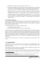
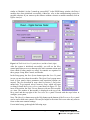
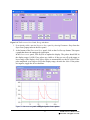
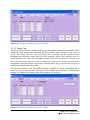
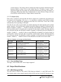
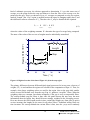
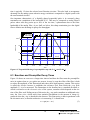
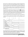
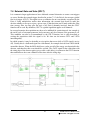
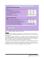
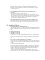
Pixie-4 Revision C/D b) Clock repeater mode c) Bussed clock master mode IN LOC JP1 JP2 BUS IN JP3 PXI BP JP3 JP1 JP2 IN JP1 JP2 LOC BUS OUT a) Individual or clock master mode JP3 JP3 PXI JP3 JP1 JP2 IN LOC JP1 JP2 JP3 JP1 JP2 Left d) Bussed clock slave mode e) PXI clock slave mode f) PXI clock master mode (slot 2 only) Figure 7.2. Jumper Settings for different clock distribution modes of Revision C modules. In a group of modules, there will be one daisy-chained clock master (a) in the leftmost position and several repeaters (b) OR one bussed clock master (c) and several bussed clock slaves (d) OR one PXI clock master (f) in slot 2 and several PXI clock slaves (e). Modes (a/b), (c/d), or (e/f) can not be mixed. Mode (e) can also be used with a custom module in slot 2 or a backplane providing 37.5 MHz instead of the usual 10MHz. 7.1.1 Individual Clock mode If only one Pixie-4 module is used in the system, or if clocks between modules do not have to be synchronized, the module should be set into individual clock mode, as shown in Figures 7.1 (a) and 7.2 (a). Connect pin 2 of JP2 (the clock input) with a shunt to pin 3 of JP2, which is labeled “LOC”. This will use the on-board clock crystal as the clock source. 7.1.2 Daisy-chained Clock Mode The preferred way to distribute clocks between modules is to daisy-chain the clocks from module to module, where each module repeats and amplifies the signal. This requires one master module, located in the leftmost slot of the group of Pixie-4 modules, with the same jumper settings as an individual module, see Figures 7.1 (a) and 7.2 (a). Configure the other modules in the chassis as clock repeaters by setting the jumpers as shown in Figures 7.1 (b) and 7.2 (b); i.e. remove all shunts from JP 1 and JP2 and set a shunt on JP3, located on top of the clock crystal U2. Note that the clock output is always enabled, i.e. every board, independent of its clock mode, sends out a clock to its right neighbor as long as it has a clock itself. Thus make sure that no other module sits to the right of a Pixie module that uses the PXI_LBR0 line on the PXI backplane for other purposes. 7.1.3 Bussed Clock Mode If there have to be gaps between a group of Pixie-4 modules, the daisy-chained clock distribution will not work since the chain is broken. In this case, the modules can be configured for bussed clock mode. To do so, configure one module (in any slot) as the bussed clock master as shown in Figures 7.1 (c) and 7.2 (c), i.e. set one shunt to connect pins 2 and 3 on JP2 and a second shunt to 56 PIXIE-4 User’s Manual V2.54 XIA 2013. All rights reserved.