1
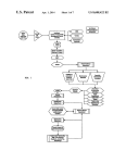
US006631510B1
(12) United States Patent
(10) Patent N0.:
(45) Date of Patent:
Betz et al.
(54) AUTOMATIC GENERATION OF
US 6,631,510 B1
Oct. 7, 2003
G. LemieuX et al., “A Detailed Router FOr Allocating Wire
Segments In FPGAs,” ACM/SIGDA Physical Design Work
shop, 1993, p. 215—226.
PROGRAMMABLE LOGIC DEVICE
ARCHITECTURES
D. Cronquist et al., “Emerald—An Architecture—Driven
Tool Compiler for FPGAs”, ACM Symp. on FPGAs, 1996,
(75) Inventors: Vaughn Betz, Toronto (CA); Jonathan
Rose, Toronto (CA)
pp. 144—150.
P. ChoW et al., The Design Of An SRAM—Based Field
(73) Assignee: Altera Toronto Co., Nova Scotia (CA)
Programmable Gate Array, Part I: Architecture, Jun. 1999,
pp. 191—197.
(*)
Notice:
Subject to any disclaimer, the term of this
patent is extended or adjusted under 35
Ebeling et al., “Placement and Routhing Tools For The
Triptych FPGA,” IEEE Trans. on VLSI, Dec. 1995, pp.
U.S.C. 154(b) by 0 days.
473—482.
G. LemieuX et al., “On TWo—Step Routing For FPGAs”,
ACM Symp. on Physical Design, 1997, pp. 60—66.
(21) Appl. No.: 09/429,013
(22) Filed:
H. Hseih et al., “ThirdiGeneration Architecture Boosts
Oct. 29, 1999
Speed And Density of Field—Programmable Gate Arrays”,
(51)
Int. Cl.7 .............................................. .. G06F 17/50
(52)
US. Cl. ........................... .. 716/16; 326/39; 326/41;
(58)
Field of Search ............................ .. 716/2, 4, 6, 11,
CICC, 1990, pp. 33.2.1—31.27.
M. Khellah et al., “Minimizing Interconnection Delays In
Array—Based FPGAs,” CICC, 1194, pp. 181—184.
716/2; 716/4; 716/6; 716/12; 716/14
* cited by examiner
716/12, 14, 16; 326/39, 41
(56)
Primary Examiner—Vuthe Siek
Assistant Examiner—Thuan Do
References Cited
(74) Attorney, Agent, or Firm—Fish & Neave; Garry J.
U.S. PATENT DOCUMENTS
5,197,016 A
5,550,839 A
Tuma
(57)
3/1993 Sugimoto et al. ............ .. 716/8
*
8/1996
Buch et al. ..... ..
ABSTRACT
.. 716/16
5,553,002 A
9/1996 Dangelo et al. ..
716/11
The invention consists of a neW component called the
5,594,657 A
1/1997 Cantone et al.
716/16
Architecture Generation Engine added to the CAD system
for implementing circuits into PLD architectures and for
5,687,325
A
5,801,546 A
5,825,202 A
11/1997
Chang
.. ... ... ..
. . . ..
9/1998 Pierce et al.
716/17
326/41
5,907,248 A
5/1999 Bauer et al.
5,942,913
8/1999
Young et al.
2/2003
Guheen et al. ............. .. 705/14
A
6,519,571 B1 *
evaluating performances of different architectures. The
Architecture Generation Engine converts a high-level, easily
speci?ed description of a PLD architecture into the highly
326/41
10/1998 Tavana et al. .
326/41
.....
detailed, complete PLD architecture database required by
. . . .. 326/41
the internals of the CAD toolset in order to map a circuit
netlist into the PLD. The Architecture Generation Engine
also enables the performance evaluation of a Wide variety of
PLD architectures for given benchmark circuits.
OTHER PUBLICATIONS
S. BroWn et al., “A Detailed Router For FIeld—Program
mable Gate Arrays”, IEEE Trans. on CAD, May 1992, pp.
26 Claims, 12 Drawing Sheets
620—628.
ARCHITECTURE
DESCRIPTION FILE
ARCHITECTURE
GENERATION ENGINE
PARSE FILE
STEP 1
CHECK FOR
FUNCTIONAL AND
SEMANTIC ERRORS
an
STEP 2
; ENUMERATE ALL BASIC
ELEMENTS
STEP 3
DESIGN ALL BASIC
STEP 4
LE ENTS
REPLICATE VARIANTS
OF THE BA C
ELEMENTS & STITCH
TILES TOGETHER
STEP 5
I
+
EVALUATE OVERALL
PLD AREA, GENERATE
STEP 6
TIMING MODELS
FULLY DETAILED PLD
TO PLD CAD TOOLS (E G.
ARCHITECTURE (E G ROUTING
RESOURCE GRAPH, TIMING GRAPH
TECHNOLOGY MAPPING.
LEGAL SLOT LIST)
PLACE AND ROUTE,
ARCHITECTURE EVALUATION)
TYPICAL FLOW DIAGRAM FOR THE ARCHITECTURE
GENERATION ENGINE
U.S. Patent
0a. 7, 2003
Sheet 1 0f 12
US 6,631,510 B1
xzo0t>3w
.wI
F
U.S. Patent
0a. 7, 2003
Sheet 2 0f 12
US 6,631,510 B1
BENCHMARK CIRCUITS
(EXAMPLE APPLICATION CIRCUITS)
V
PLD ARCHITECTURE
DESCRIPTION
COMPUTER-AIDED DESIGN SYSTEM
TARGETTING PLD ARCHITECTURE
OF INTEREST
EVALUATE QUALITY OF
BENCHMARK CIRCUIT IMPLEMENTATIONS
IN PLD ARCHITECTURE
TYPICAL PLD ARCHITECTURE EVALUATION FLOW DIAGRAM
FIG. 2
U.S. Patent
Oct. 7,2003
Sheet 3 0f 12
US 6,631,510 B1
BENCHMARK
CIRCUITIS)
HIGH-LEVEL
, ARCHITECTURE
DESCRIPTION
I _____ _ _ I; _____ _ _I
I
SYSTHESIS AND LOGIC
I PLD
,
OPTIMIZATION
I CAD
I
V
l
TECHNOLOGY
I
I TOOLS
I
MAPPING
I
I
ARCHITECTURE
GENERATION
ENGINE
I
I T
I
L.
_
_
‘
I
PLACE AND ROUTE
l
I
_
‘
_
_
_
i_
_
_
_
_
_.
_
J
EVALUATE PLD
PERFORMANCE
ADJUST PLD
PARAMETERS
YES
CHANGE PLD
PARAMETERS?
PLD ARCHITECTURE
EVALUATION
COMPLETED
CAD FLOW DIAGRAM PROPOSED BY THIS INVENTION FOR
PLD ARCHITECTURE GENERATION AND EVALUATION
FIG. 3
U.S. Patent
0a. 7, 2003
Sheet 4 0f 12
US 6,631,510 B1
CONNECTION
BLOCK
POPULATION:
100%
80%
60%
40%
POSSIBLE CONNECTION-BLOCK POPULATION VALUES FOR
LENGTH 5 WIRE SEGMENTS.
FIG. 4
U.S. Patent
0a. 7, 2003
io_rat 2
chan_width_io 1
Sheet 5 0f 12
US 6,631,510 B1
# 2 l0 pads per row or column
# All channels the same width.
chan_width_x uniform 1
chan_width_y uniform 1
# 4-input LUT. LUT inputs first, then output, then clock.
inpin class: 0 bottom
inpin class: 0 left
# Equivalence class 0 is LUT inputs
inpin class: 0 top
inpin class: 0 right
outpin class: 1 bottom
inpin class: 2 global top
# Output. Not equivalent to anything.
# Clock.
switch_block_type subset
# Called disjoint switch block by some.
Fc_type fractional
# Fc values are relative to W
Fc_output 1
Fc_input 1
Fc_pad 1
# Definitions of different types of routing wires.
segment frequency: 0.2 length: 1wire_switch: 0 opin__switch: 1 Frac_cb: 1.\
Frac_sb: 1. Rmetal: 4.16Cmetal: 81e-15
segment frequency: 0.4 length: 2 wire_switch: 2 opin_switch: 2\
Frac_cb: 1. Frac_ab: 1Rmetal: 4.16 Cmetal: 8le-15
segment frequency: 0.4 length: 4wire_switch: 2opin_switch: 2\
Frac_cb: 1. Frac_sb: 1Rmetal: 4.16Cmetal: 81e-15
# Definitions of different types of routing switches.
# Pass transistor switch.
switch 0 buffered: no R: 196.728 Cin: 20.574e-15 Cout: 20.574e-15 Tdel: 0
# Logic block output buffer used to drive pass transistor switched wires.
switch 1 buffered: yes R: 393.47 Cin: 7.512e-15 Cout: 20.574e-15 Tdel: 524e-12
# Switch used as a tri-state buffer within the routing, and also as the
# output buffer used to drive tri-state buffer switched wires.
switch 2 buffered: yes R: 786.9 Cin: 7.512e-15 Cout: 10.762e-15 Tdel: 456e-12
# Used only by the area model.
R_minW_nmos 1967
R__minW_pmos 3738
# Timing info below. See manual for details.
C_ipin_cblock ‘1.512e-15
T_ipin_cblock 1.5e-9
T_ipad 478e-12
# clk_to__Q + 2:1 mux
T_opad 295e-12
# Tsetup
T_sblk_opin_to_sblk_ipin o.
T_clb_ipin_to_sblk_ipin o.
F|G_ 5
.
Examplearchltecture
descrlpilon ?le
T_sblk_opin_to_clb_opin 0.
subblocks_per_clb 1
subblock_lut_size 4
T_subblock T_comb: 546e-12 T_seq_in: 845e-12 T_seq_out: 478e-12
U.S. Patent
061. 7, 2003
WIRE
Sheet 6 6f 12
US 6,631,510 B1
WIRE
MODELLING FPGA ROUTING ARCHITECTURE AS A DIRECTED GRAPH
FIG. 6
U.S. Patent
Oct. 7, 2003
Sheet 7 0f 12
US 6,631,510 B1
ARCHITECTURE
DESCRIPTION FILE
ARCHITECTURE
GENERATION ENGINE
\
PARSE FILE
STEP 1
V
CHECKFOR
FUNCTIONAL AND
SEMANTIC ERRORS
STEP 2
\
ENUMERATE ALL BASIC
ELEMENTS
STEP 3
V
DESIGN ALL BASIC
ELEMENTS
STEP 4
\
REPLICATE vARIANTS
OF THE BASIC
STEP 5
ELEMENTS & STITCH
TILES TOGETHER
\
EVALUATE OvERALL
PLD AREA, GENERATE
TIMING MODELS
STEP 6
FULLY DETAILED PLD
ARCHITECTURE (E.G. ROUTING
RESOURCE GRAPH, TIMING GRAPH
LEGAL SLOT LIST)
TO PLD CAD TOOLS (E.G.
TECHNOLOGY MAPPING,
PLACE AND ROUTE,
ARCHITECTURE EVALUATION)
TYPICAL FLOW DIAGRAM FOR THE ARCHITECTURE
GENERATION ENGINE
FIG. 7
U.S. Patent
0a. 7, 2003
Sheet 8 0f 12
US 6,631,510 B1
ROUTING
WIRE
'
\ ROUTING
SWITCH
FIG. 8(a)
EXAMPLE CONNECTION BLOCK PATTERN: PATHOLOGICALLY BAD
NETS STARTING AT OUT2 CAN ONLY REACH IN2,
NETS STARTING AT OUT1 CAN ONLY REACH IN1.
FIG. 8(b)
EXAMPLE CONNECTION BLOCK PATTERN: GOOD.
NETS STARTING AT EITHER OUTPUT CAN REACH
EITHER INPUT; VASTLY IMPROVED ROUTABILITY
U.S. Patent
0a. 7, 2003
Sheet 9 0f 12
US 6,631,510 B1
PROGRAMMABLE
SWITCH
l
\ WIRE SEGMENT
FIG. 9(a)
ARCHITECTURE SPECIFICATION: DISJOINT SWITCH BLOCK
SEGMENT "START POINTS"
/\
\
E/
FIG. 9(0)
ARCHITECTURE SPECIFICATION: SEGMENTATION DISTRIBUTION.
EACH CHANNEL CONTAINS 3 WIRES OF
LENGTH THREE.
U.S. Patent
0a. 7, 2003
Sheet 10 0f 12
US 6,631,510 B1
z“g2b0a:c5mn; 295t986Mo:2
_.Jkz6w/Eomw
GI2
U.S. Patent
0a. 7, 2003
. .40
Sheet 12 0f 12
4/
US 6,631,510 B1
A
P.
w“.wE
2m39;5
US 6,631,510 B1
1
2
AUTOMATIC GENERATION OF
PROGRAMMABLE LOGIC DEVICE
ARCHITECTURES
HoWever, in order to implement circuits in a PLD archi
tecture of interest, the PLD designer requires a method of
describing the PLD architecture to the CAD tool set. There
are tWo basic components of a PLD architecture: the routing
architecture Which describes the routing resources or the
This invention relates generally to Programmable Logic
programmable interconnect netWork; and the logic (or
Devices (PLDs), and more particularly to a method and
function) block architecture. Consider ?rst the problem of
describing the PLD routing architecture.
system for generation and evaluation of architectures for
such devices.
BACKGROUND OF THE INVENTION
To specify a PLD architecture in its entirety, one must
10
Programmable Logic Devices (PLDs) are a Widely used
form of integrated circuit due to the ?exibility provided by
Wires and logic and I/O blocks can be interconnected by
programmable sWitches, and the delay of every program
mable sWitch, routing Wire and circuit path through a logic
their customiZable nature. In general PLDs include ?eld
programmable gate arrays (FPGAs), complex program
mable logic devices (CPLDs), simple programmable logic
15 block in the entire PLD. This is an enormous amount of
data—typically tens to hundreds of MB in siZe. Accordingly,
it is not practical for a PLD architect to specify this data
directly for every PLD architecture in Which he or she is
interested.
The most straightforWard Way of describing a PLD rout
ing architecture is to create a directed graph (also called a
devices and laser programmable devices. Architecturally, a
PLD includes logic blocks and input/output (I/O) blocks
Which are connectable through a programmable interconnect
structure.
Atypical PLD is an integrated circuit chip that, Wholly or
in part, consists of an array of one or more logic blocks, I/O
routing-resource graph) that fully speci?es all the connec
blocks, and a programmable routing or interconnect net
Work. The interconnect netWork can be programmed by a
user to provide a connection betWeen the logic and I/O
blocks to achieve a desired logic function. A PLD can be a 25
standalone device or be embedded in a larger integrated
circuit such as ASICs or the like. Exemplary forms of such
embedded PLDs are disclosed in US. Pat. No. 5,825,202
and US. Pat. No. 5,687,325.
The logic blocks may be comprised of a ?xed logic
nection pin is located. This description must specify Which
routing Wires, logic blocks and I/O blocks can be intercon
nected by programmable sWitches. The description must
also specify the delay of every programmable sWitch, inter
connect Wire and circuit path through a logic block, in the
and is typically the data structure used internally by the
routing tool. HoWever, it is not very practical to specify this
nect netWorks and programmable functionality. The logic
routing-resource graph manually because the routing
35
cuits or to other parts of the chip as in the case of an
resource graph for a typical PLD requires an enormous
amount of data—typically in the tens to hundreds of mega
bytes of memory in siZe. Essentially, this is too loW-level a
description for a PLD architect to use conveniently.
A more practical approach is to design a basic tile
embedded PLD. The 1/0 blocks are typically arranged at the
periphery of a chip.
A PLD is typically arranged as a regular array of logic
(consisting of a single logic block and its associated routing)
blocks, each of Which may be identical or may be one of
manually, and create a program to automatically replicate
and stitch together this tile into a routing-resource graph
several different types (such as memory blocks, look-up
table based blocks, p-term based blocks etc.). The conduc
tors of the programmable interconnect netWork are typically
arranged along roWs and columns de?ed by the array of
logic blocks, as shoWn schematically in FIG. 1.
The architecture of a PLD speci?es the structure of its
tions that may be made in the routing of a circuit in the PLD.
In essence, this requires the PLD designer to describe Where
every sWitch, interconnect Wire, logic and 1/0 block con
entire PLD. This is a very general representation of a PLD
function or may in turn also have programmable intercon
blocks may be ?rer broken doWn into sub-blocks or grouped
together as a cluster of logic blocks. These blocks may also
include I/O circuits that enable connection to external cir
specify Where every sWitch, routing Wire and logic and IO
block pin is located One must also specify Which routing
describing the entire PLD routing architecture. HoWever,
even the manual creation of a basic tile can be too time
45
consuming for most PLD architectures. A typical tile con
tains several hundred programmable sWitches and Wires, so
it can take hours or days to describe a single tile.
logic blocks, I/O blocks and programmable interconnect
Furthermore, the hand-crafted tile is severely limited in the
netWork. In order to develop a high-quality PLD
PLD interconnect or logic block resources that may be
architecture, the PLD designer must evaluate the impact and
utility of a Wide range of architectural decisions and trade
offs. The performance of a PLD is typically judged on the
varied—for example, a hand-crafted tile is generally
designed for one value of the routing channel Width, W (the
number of routing tracks in a channel). In many architecture
basis of operational parameters of circuits implemented in
the PLD. These operational parameters include speed of
experiments, one must vary W in order to see hoW routable
a given PLD architecture is, or to determine the minimum
circuits implemented in the PLD, semiconductor or silicon
area required to implement a given circuit in the PLD, poWer
dissipation of the PLD after it has been programmed,
55
circuits (say 95%) to route successfully. With a tile based
approach, the PLD designer must hand-craft different tiles
for each different value of W required to be tested. A PLD
designer Will often Wish to investigate hundreds of different
reliability and routing ?exibility.
The typical procedure for evaluating different architec
tures is shoWn in FIG. 2. A set of benchmark circuits is
implemented in each PLD architecture (or architecture
variant) of interest, and the operational parameters of the
circuits are analyZed. Generally, PLD designers Wish to
experiment With as Wide a variety of PLD architectures as
possible in order to determine the architecture or class of
architectures that best meets the operational parameters of
interest.
value of W that alloWs some desired faction of application
65
PLD architectures and tens of W values for each of these
architectures. The net result is that the PLD designer is
required to create thousands or tens of tho of different basic
tiles.
There has been some prior Work in describing PLD
routing at a higher level of abstraction. In [1], BroWn et al
developed an FPGA router for use With island-style FPGAs.
In order to quickly investigate FPGAs With different num
US 6,631,510 B1
4
3
generating a detailed description from the complete PLD
bers of routing switches, they localized all the code that
architecture, for use by a CAD toolset
By
interacted
reWriting
Withthese
switchtWo
patterns
routines,
to tWo
theroutines,
FPGA designer
FC() and can
target their router (called CGE) to an FPGA With different
sWitch pattern. The later SEGA router [2], used the same
method to alloW re-targetting to different FPGAs.
In the Emerald CAD system [3], an FPGA’s routing is
described by means of WireC schernatics—essentially sche
matics annotated With C-language like code that describes
sWitch patters. The Emerald system can convert these WireC
schematics into routing-resource graphs for use by its FPGA
BRIEF DESCRIPTION OF THE DRAWINGS
These and other features of the preferred embodiments of
the invention Will become more apparent in the folloWing
detailed description in Which reference is made to the
appended draWings Wherein:
10
according to the prior art;
router.
FIG. 3 is a schematic ?oW diagram of shoWing an
architecture generation system according to an embodiment
While CGE, SEGA and Emerald all reduce the labour
required to specify a PLD architecture, they still require
considerable hand-crafting effort. Instead of specifying
FIG. 1 is a block diagram of a typical PLD architecture;
FIG. 2 is a PLD architecture evaluation ?oW diagram
15
every sWitch in a basic tile of an FPGA, these systems alloW
PLD designers to Write softWare code (in either C or WireC)
to generate all the sWitches in a basic tile. If the PLD
designer Writes suf?ciently general code, it may be possible
of the present invention;
FIG. 4 is a schematic diagram shoWing the possible
connection-block population values for length 5 Wire seg
ments;
FIG. 5 shoWs an eXample architecture description ?le;
FIG. 6 shoWs an hoW an eXample architecture can be
to change some interconnect and logic resources, such as the
modelled using a directed graph;
FIG. 7 shoWs the typical ?oW diagram for the Architecture
channel Width W, and have the basic tile adapt properly.
HoWever, it is the user’s task to specify this in often
non-obvious code.
The second portion of a PLD architecture description
details each type of function block (logic or 1/0 block)
contained in the PLD. Both the interface to the PLD routing
of each function block (i.e. a list of the inputs and outputs of
the block) and a description of the logic functions that can
Generation Engine;
FIG. 8(a) shoWs a connection block pattern that is patho
logically bad;
FIG. 8(b) shoWs a connection block pattern that is good;
FIG. 9(a) is an architecture speci?cation for a disjoint
be implemented by the function block, must be provided. A
sWitch block;
FIG. 9(b) is an architecture speci?cation for segmentation
concise method for providing this information is crucial to
distribution;
alloW easy experimentation.
As Well, timing and area model information for both the
routing and function blocks may be included in the PLD
architecture description, to alloW the CAD tools to estimate
the speed achieved by the circuits in this architecture, and
the layout area consumed by the architecture.
FIG. 10 shoWs hoW replicating one channel causes hori
Zontal and vertical constraints to con?ict;
FIG. 11 shoWs hoW adjusting the segment start points
35
FIG. 12 shoWs the tiled layout used to implement the PLD
architecture of FIG. 11 above.
Accordingly, there is a need for a method and system that
reduces the labour involved in describing a complete PLD
architecture and alloWs the easy variation of many intercon
nect and logic resource parameters of the architecture.
DETAILED DESCRIPTION OF THE
PREFERRED EMBODIMENT
Preferably, the architecture generation engine converts a
concise high-level description of a PLD architecture into the
SUMMARY OF THE INVENTION
In accordance With this invention there is provided a
system for generating a PLD architecture comprising:
an Architecture Generation Engine for converting a high
level, easily speci?ed description of a PLD architecture
alloWs both the horiZontal and vertical constraints to be
satis?ed Within a PLD coordinate system; and
fully detailed description required by the CAD tools to
45
implement circuits in the PLD and to estimate the perfor
mance of the architecture. A preferred implementation of
hoW to represent a PLD architecture concisely, and to
automatically generate the fully detailed representation of
into the highly detailed, complete PLD architecture
database; the detailed PLD architecture used by the
the architecture is described beloW. Many variations on this
CAD toolset to map a circuit netlist into the PLD.
In a further embodiment, the Architecture Generation
using only a subset of the parameters listed beloW to
preferred implementation are possible, hoWever, including
Engine also enables the performance evaluation of a Wide
variety of PLD architectures for given benchmark circuits.
In a further embodiment of the invention, there is pro
vided a CAD system for implementing circuits into PLD
architectures and for evaluating performances of different
describe a PLD, or using a different set of parameters.
55
the Wire length (number of logic blocks spanned), and
architectures.
In accordance With a further embodiment of the invention,
there is provided a method for generating an architecture for
the Wire resistance and capacitance, or other delay
metric;
The various “types” of programmable routing sWitch used
a programmable logic device (PLD), the method comprising
in the PLD, including Whether each sWitch is a pass
the steps of:
creating a data ?le de?ning a high-level architecture
transistor, tri-state buffer, multiplexer, antifuse, etc.; the
delay of the sWitch, (Which may be a ?ll delay model,
description of the programmable logic device;
creating unique functional elements of the PLD generally
matching the description in the data ?le;
replicating and stitching together the functional elements
to create a complete PLD architecture; and
Using a high-level PLD architecture description language,
the PLD designer describes the architecture using:
The various “types” of Wire used in the PLD, including
such as the Elmore delay or a SPICE delay model,
rather than a simple delay number); and the area of the
65
sWitch, or some parameter such as equivalent resistance
Which alloWs an area model to estimate the area of the
sWitch;
US 6,631,510 B1
6
5
Each type of logic block and I/O block in the PLD,
including a list of the input and output pins of each
choices must be made for the unspeci?ed interactions
betWeen parameters and unspeci?ed portions of the archi
tecture in order to create a PLD architecture that matches the
block, any logical equivalences betWeen these pins, and
the physical side(s) from Which each pin is accessible;
speci?ed parameters and has good area and speed.
Another dif?culty is that the speci?ed parameters may
The number of blocks of each type Which can be placed
con?ict and overspecify the PLD. In this case the architec
ture generator must relax the speci?cation (in as small an
at each physical (i,j) location Within the PLD;
The relative Widths of the various channels Within the
amount as possible) to create a PLD that still matches most
PLD;
of the speci?ed parameters.
In addition to creating the fully speci?ed detailed PLD
architecture database required by the PLD CAD tools, the
Either the faction or the absolute number of routing tracks
in each type of channel that consist of Wires of a given
architecture generation engine can also automatically com
pute important metrics of the PLD architecture quality. The
metrics it computes include:
type;
The number and type of sWitches alloWing each logic
block pin to connect to each channel near it, or option
ally a more detailed description of the pate of sWitches
15
The estimated area required to build this PLD. The
betWeen each logic block pin and the Wires in the
architecture generation engine can compute this by
channels near it;
traversing the detailed PLD description (the routing
resource graph and the legal slot list), and using built-in
The number and type of sWitches used to connect routing
Wires of each type to each other, or optionally, the set
of sWitch patterns to be used to connect Wires in the
routing channels can be speci?ed;
The delay through each of the combinational and sequen
area models to estimate the area required by each Wire
and sWitch in the programmable routing, and by each
logic or I/O block. This area estimate can be based on
metal area, active area or both.
tial paths through each type of logic and I/O block.
Optionally his delay may be a delay model, rather than
a constant delay number for each path.
25
Other parameters Which may be either speci?ed by the
PLD architect, or Which the CAD toolset can determine
automatically such that a given application circuit Will ?t
proposed by this invention for the generation and evaluation
of PLD architectures. The starting point of the invention is
into the generated PLD architecture are:
The absolute Width (in routing tracks) of some or all of the
the realiZation that in order to make descriptions of PLD
architectures easy to create, they must be parameteriZed in
Ways that are intuitive to PLD designers. Essentially, the
PLD is described in a high-level PLD architecture speci?
routing channels;
The number of logic blocks in the PLD (i.e. the siZe of the
array of logic blocks).
The architecture generation engine takes this list of
parameters or constraints, and generates the highly detailed
The estimated delay of a circuit implemented in this PLD.
The estimated poWer consumption of a circuit imple
mented in this PLD.
The estimated PLD area required by the circuit imple
mented in the PLD.
FIG. 3 shoWs the an example of the overall design How
35
description of the architecture required by the CAD optimi
cation language. The architecture generation engine con
verts the high-level description of the PLD architecture into
the fully detailed description required by the CAD tools to
implement circuits in the PLD. The fully detailed description
Zation tools to map circuits into the architecture. For
example, this detailed architecture description may consist
can also be used to estimate the operational parameters of
of:
circuits implemented by this architecture.
A directed graph (the routing resource graph) that
To make this discussion more concrete, a preferred imple
describes every element of a PLD’s programmable
interconnect. Each node in this graph corresponds to a
mentation of hoW to represent a PLD architecture in a
“routing resource”, eg a logic block or I/O block pin,
a routing Wire, a routing multiplexer or other routing
element Each edge in this graph corresponds to a
erate the fully detailed representation of the architecture is
described here. Many variations on this preferred embodi
ment are possible, hoWever, including using only a subset of
high-level description language, and to automatically gen
45
possible connection (made via a programmable sWitch)
the listed parameters or using a different set of parameters.
For a typical implementation of a PLD (such as that
betWeen routing resources. Some edges may be
inserted to model non-programmable sWitches or to
shoWn in FIG. 1), the high-level description ?le Would
include speci?cation of the folloWing parameters:
assist delay modelling. Every edge and every node is
annotated With information concerning its physical
The interconnect Wires segments used in the PLD. For
each Wire segment type, the folloWing parameters can
implementation (e.g. is it a Wire or a pin, hoW long is
the Wire, etc.) and its delay parameters.
A directed graph (the timing graph) that explicitly repre
sents the circuit timing When implemented in this
architecture. Every edge in this graph represents a
timing dependency, and every node represents a circuit
be speci?ed:
55
pin or function.
metric;
Alegal slot list that describes Which type(s) of logic or I/O
block can be assigned to each (i,j) location Within the
The fraction or the absolute number of tracks in a
channel that are of this segment type;
The type of sWitch (pass-transistor or tri-state buffer,
drive strength of the sWitch) used to connect a Wire
segment of this type to other routing segments;
The sWitch-block internal population of this segment
PLD.
There are numerous difficulties associated With the auto
matic generation of this fully detailed representation of the
PLD from the concise, architecture description language
version.
One dif?culty is that the speci?ed parameters often do not
completely specify the entire PLD architecture. Intelligent
The segment length or the number of logic blocks
spanned by a Wire segment;
The Wire Width and spacing betWeen adjacent Wires or
the Wire resistance and capacitance or other delay
65
type (discussed beloW); and
The connection-block internal population of this seg
ment type (discussed beloW).
US 6,631,510 B1
8
7
expanded to include the notion of partial depopulation. For
example, a length ?ve segment spans ?ve logic blocks. If We
specify a connection-block population of 100%, this Wire
The programmable routing switches used in the PLD,
including:
Type of switch (e.g. pass-transistor, tri-state buffer,
segment can connect to all ?ve logic blocks it passes, so it
multiplexer, antifuse, laser programmable, etc.);
is fully internally populated. If the connection-block popu
The delay of the sWitch (Which may be a description of
lation is 40%, it can only connect to the tWo logic blocks at
its ends, so it is internally depopulated. If We specify a
the delay model such as the Elmore delay or SPICE
delay model, or a simple delay number); and
Area of the sWitch or some other parameter such as the
equivalent resistance that alloWs an area model to
estimate the area of the sWitch.
connection-block population of 60%, hoWever, the Wire can
connect to the tWo logic blocks at its ends and one logic
10
Each type of logic block and I/O block in the PLD,
including a list of the input and output pins of each
block population for a length ?ve Wire. Switch-block popu
lation is speci?ed in a similar, percentage, form.
Notice that the distribution of Wire types can be speci?ed
block, any logical equivalence betWeen these pins, and
the physical side or sides from Which each pin is
accessible. Logical equivalence refers to nodes that are
functionally equivalent, such as all the inputs of a
15
look-up table;
user to evaluate architectures With different W values, to
determine the routability of an architecture, Without chang
ing the architecture ?le.
sub-components of each function block; or
Abinary decision tree diagram of all logic functions the
Similarly, the various FC values can be speci?ed either as
absolute numbers (e. g. 5 tracks), or as a fraction of the tracks
block can implement; or
25
in a channel (e.g. 0.2*W).
Other parameters Which may be either speci?ed by the
PLD designer or Which the CAD tool set can determine
The number of logic or I/O blocks of each type that can
be placed at each physical location Within a PLD;
The relative Widths of the various routing channels in the
automatically such that a given application circuit Will ?t
into the generated PLD architecture are:
The absolute Width (in routing tracks) of some or all of the
PLD;
routing channels;
The sWitch block topology used to connect the routing
The number of logic blocks in the PLD (i.e. the siZe of the
array of logic blocks).
tracks (i.e. Which tracks connect to Which at a sWitch
block—a sWitch block is the point Where horiZontal and
vertical routing channels intersect);
The number (Fm-Wm) and type of sWitches alloWing each
as factions of the channel Width, W, rather than as an
absolute number of tracks of each type. For example, the
PLD designer might specify that there are 20% Wires having
length 2 and 80% of Wires having length 5. This alloWs a
Description of the internal functionality of the logic and
I/O blocks including:
Number, type and permissible connections betWeen the
Logic library of all the logic functions the block and/or
sub-components can perform.
block in its interior, so it is partially internally depopulated.
FIG. 4 illustrates the four possible values of connection
35
logic block input pin to connect to each channel near it,
FIG. 5 shoWs a high-level architecture description ?le for
a PLD in Which the logic block is a 4-input look-up table
plus a register. The description is concise and conveys all the
information that the PLD designer Would need to completely
or optionally, a more detailed description of the pattern
describe the PLD architecture of interest. While this is a
of sWitches betWeen each logic block input pin and the
simple example, even complex PLD architectures can be
easily described in the same concise, but precise methodol
Wires in the channel near it;
ogy. The “VPR User Manual,” incorporated herein by
reference, explains the design and syntax of the description
The number (Fcpmpm) and type of sWitches alloWing each
logic block output pin to connect to each channel near
it, or optionally, a more detailed description of the
?le. The VPR User Manual also explains the terminology
used in the architecture description ?le.
pattern of sWitches betWeen each logic block output pin
While the architecture parameters listed above are easy
and the Wires in the channel near it;
The number (FCWd) and type of sWitches alloWing each
45
appropriate for use as an internal architecture representation
for a router. Internally, the CAD tools use a routing-resource
I/ O block input or output pin to connect to each channel
near it, or optionally, a more detailed description of the
graph [5] to describe the PLD; this is more general than any
pattern of sWitches betWeen each logic block output pin
parameteriZation, since it can specify arbitrary connectivity.
and the Wires in the channel near it;
The number and type of sWitches used to connect routing
Wires of each type to each other, or optionally, the set
of sWitch patterns to be used to connect Wires in the
It also makes it much faster to determine connectivity
information, such as the Wires to Which a given Wire
segment can connect, since this information is explicitly
contained in the graph.
routing channels;
The delay through each of the combinational and sequen
tial paths through each type of logic and I/O block.
Optionally, this delay may be a delay model, rather than
a constant delay number for each path.
TWo of the parameters listed above, sWitch-block and
connection-block internal population, may not be familiar to
many PLD researchers. These tWo terms Were introduced by
ChoW et al in
They indicate Whether or not routing Wires
and logic blocks, respectively, can connect to the interior of
a Wire segment that spans multiple logic blocks, or if
connections to a Wire can be made only at its ends. In [4],
a Wire segment is either completely internally populated or
completely depopulated, hoWever, this concept can be
for PLD designers to understand and specify, they are not
55
Each Wire and each logic block pin becomes a node in this
routing-resource graph and each sWitch becomes a directed
edge (for uni-directional sWitches, such as buffers) or a pair
of directed edges (for bi-directional sWitches, such as pass
transistors) betWeen the tWo appropriate nodes. FIG. 6
shoWs the routing-resource graph corresponding to a portion
of a PLD Whose logic block contains a single 2-input,
1-output look-up table (LUT).
Often PLD logic blocks have logically equivalent pins;
for example, all the input pins to a LUT are logically
equivalent. This means that a router can complete a given
65
connection using any one of the input pins of a LUT;
changing the values stored in the LUT can compensate for
any re-ordering of Which connection connects to Which input
US 6,631,510 B1
9
10
pin performed by the router. We model this logical equiva
lence in the routing-resource graph by adding source nodes
In step 3, the architecture generation engine determines all
the unique “basic elements” Which Will have to be generated
in order to create the speci?ed PLD architecture. Typically,
the unique basic elements Will be one of each function block
at Which all nets begin, and sink nodes at Which all net
terminals end. There is one source node for each set of
logically-equivalent output pins, and there is an edge from
(IO or logic block) speci?ed, all the unique horiZontal and
the source to each of these output pins. Similarly, there is
one sink node for each set of logically-equivalent input pins,
and an edge from each of these input pins to the sink node.
To reduce the number of nodes in the routing-resource
vertical channels (i.e. one of each different type of routing
graph, and hence save memory, We assign a capacity to each
channel speci?ed) and all the unique sWitch patterns
required by the architecture. Typically the unique sWitch
patterns Will consist of one connection box (function block
10
node. A node’s capacity is the maximum number of different
nets Which can use this node in a legal routing. Wire
pins to routing Wires sWitch pattern) for each side of each
type of function block, and one sWitch block (sWitch patter
governing the connection of routing Wires to other routing
segments and logic block pins have capacity one, since only
Wires) for each distinct pair of crossing channels (usually
one net may use each. Sinks and sources can have larger
of four logically-equivalent inputs, so We have one sink of
capacity four. If We could not assign a capacity of four to the
sink, We Would be forced to create four logically-equivalent
vertical and horiZontal channels).
In step 4, each of the unique basic elements is generated.
To generate each unique channel, for example, the number
of Wires in this type of channel is determined, the type
(length, speed, etc.) of each Wire in this channel is ?xed, and
sinks and connect them to the four input pins via a complete
the break points at Which Wire segments end are chosen. To
bipartite graph (K4>4), Wasting considerable memory.
generate each unique sWitch pattern, heuristic algorithms
capacities. For example, in a 4-input LUT, there is one group
15
To perform timing-driven routing, ting analysis, and to
may be used in order to construct a sWitch pattern that meets
graphically display the architecture We need more informa
tion than just the raW connectivity embodied in the nodes
the speci?cations on the number and type of sWitches to be
used, hoW many sWitches should attach to each Wire or pin
and edges of the routing-resource graph Accordingly, We
notate each node in the graph With its type (Wire, input pin,
etc.), location in the PLD array, capacitance and metal
resistance. Each edge in the graph is marked With the index
of its “sWitch type,” alloWing retrieval of information about
the sWitch intrinsic delay, equivalent resistance, input and
(and any other speci?cations) and that results in good
25
routability (i.e. a good PLD). The problem of generating
good sWitches patterns is discussed in more detail later in
this description. Once all the basic elements have been
generated, the architecture generation engine moves on to
step 5, Where it replicates variants of these basic elements
output capacitance and Whether the sWitch is a pass transis
and stitches them together to create a PLD that matches all
tor or tri-state buffer.
the architectural speci?cations, and that is easy to lay out As
described later in this description, creating an entire PLD
As described earlier, there arc compelling reasons to
alloW PLD designers to specify architectures in an
from these basic patterns is more complex than simply
understandable, parameteriZed format, and for the routing
replicating these sWitch patterns and basic channels across
the PLD—they must be stitched together in a more involved
tools to Work With a more detailed (e.g. graph-based)
35
description. We therefore need the capability illustrated in
Way.
FIG. 3: a tool that can automatically generate a detailed
Finally, in step 6, the architecture generation engine can
architecture description (including the routing-resource
traverse the data structures de?ning the noW fully-detailed
graph) from a set of speci?ed architecture parameters. This
PLD architecture, and apply built-in area, delay, and poWer
is a dif?cult problem for tWo reasons;
1. We Want to create a good architecture With the speci?ed
models to each circuit element making up the architecture.
The output of this stage is an estimate of the PLD area, and
parameters. That is, the unspeci?ed properties of the archi
an estimate of the PLD delay and poWer, or a delay and
poWer model of the entire PLD that can be used to estimate
tecture should be set to “reasonable” values.
2. Simultaneously satisfying all the parameters de?ning the
architecture is dif?cult. In some cases, the speci?ed param
45
eters con?ict and over-specify the FPGA, making it impos
sible to simultaneously satisfy all the speci?ed constraints.
FIG. 7 shoWs the typical ?oW diagram for the architecture
generation engine. Step one consists of simply parsing the
architecture description ?le into the internal data structures
the speed and poWer consumption of an application circuit
implemented in this PLD architecture.
The fully detailed PLD architecture can then be Written
out to ?les, or transferred through memory, to a CAD tool or
CAD tool set that can automatically implement application
circuits in the PLD.
of the architecture generation engine. In step tWo, the
architecture generation engine checks for both semantic
DIFFICULTIES IN PLD ARCHITECTURE
GENERATION
errors (such as missing or invalid PLD architecture descrip
There are tWo major dif?culties that arise in automatically
generating PLD architectures in this Way. The ?rst dif?culty
arises because the PLD designer is not required to specify
every conceivable parameter and every possible interaction
betWeen all parameters.
Instead, the focus of the high-level architecture descrip
tion methodology is to enable the PLD designer to specify
the important parameters and have the architecture generator
automatically adjust other parameters of the architecture so
tion language keyWords) and functional errors. Functional
errors are more subtle than semantic errors—they involve 55
specifying a PLD Which is either not realiZable, or is
obviously a very poor (e.g. unroutable) PLD architecture.
Examples of functional errors include specifying a PLD in
Which certain logic block input or output pins cannot con
nect to any Wires, specifying Wires Which cannot be reached
(via programmable sWitches) from any other Wire or func
tion block pin, or specifying an architecture in Which there
are no routing paths betWeen certain function blocks. When
such functional errors are found, the architecture generation
that a good PLD architecture results. Consider an example
that occurs in step 4 of FIG. 7. The high-level architecture
description methodology requires that the PLD designer
tool immediately informs the user to enable the error to be 65 specify the number of tracks to Which input and output pins
corrected before much time is spent analyZing this very poor
PLD architecture.
can connect, Fcmpm and Fcpmpm, rather than requiring a user
to specify the complete connection block sWitch pattern.
US 6,631,510 B1
11
12
This certainly simpli?es the task of describing an PLD, but
Wire segments Which the sWitch block and internal popula
tion parameters indicate should be connected. FIG. 10 shoWs
it means that the architecture generation engine must gen
erate a good connection block sWitch pattern automatically.
the results of such a technique, Where only a feW of the
routing sWitches have been shoWn for clarity. Notice that
this PLD does not meet the speci?cations. By inserting
Let us consider this connection block problem in more
detail. We decided that the sWitch pattern chosen should;
10
routing sWitches at the ends of the horiZontal segments, We
are alloWing connections into the middle of vertical seg
ments. HoWever, our speci?cations said that segments
should have routing sWitches only at their ends. If We do not
insert sWitches at the ends of the horiZontal segments,
15
segments, so the speci?cations are again violated, We call
this problem a con?ict betWeen the horiZontal constraints
and the vertical constraints.
The solution to this problem is shoWn in FIG. 11. Instead
Ensure that each of the W tracks in a channel can be
connected to roughly the same number of input pins,
and roughly the same number of output pins,
Ensure that each pin can connect to a mix of different Wire
types (eg different length Wires),
hoWever, We cannot connect to the ends of the horiZontal
Ensure that pins that appear on multiple sides of the logic
block connect to different tracks on each side, to alloW
more routing options,
Ensure that logically-equivalent pins connect to different
tracks, again to alloW more routing options, and
Ensure that pathological sWitch topologies in Which it is
impossible to route from certain output pins to certain
input pins do not occur. FIG. 8 shoWs one example of
a pathologically bad sWitch pattern—some logic block
output pins cannot drive any tracks that can reach
of simply replicating a single channel, the “start points” of
20
certain input pins.
Clearly this is a complex problem. In essence, the proper
of this “segment start point adjustment” technique—We not
connection block pattern is a function of FCJ-npm, Fqompm, W,
the segmentation distribution (lengths of routing Wires), the
logical equivalence betWeen pins, and the side(s) of a logic
25
only meet our speci?cations fully, but create an easily
laid-out PLD.
In order to describe the adjustment of the segment start
points more clearly, let us de?ne a PLD coordinate system.
Let the logic block in the loWer left corner of the logic block
30
array have coordinates (1,1). The logic block to its right has
coordinates (2,1), and the logic block above it has coordi
block from Which each pin is accessible. The last condition
is also a function of the sWitch block topology. The archi
tecture generator Would typically use a heuristic algorithm
that attempts to build a connection block that satis?es the
?ve criteria above, but it Will not necessarily perfectly
satisfy them all for all architectures.
The second dif?culty in generating an architecture auto
nates (1,2), as FIG. 11 shoWs. A horiZontal channel has the
same y-coordinate as the logic block beloW it, and a vertical
matically is simultaneously meeting all the user-de?ned
speci?cations. We Will illustrate this dif?culty With an
example that shoWs it often takes considerable thought to
the segments in each channel have to be adjusted. As FIG.
11 shoWs, this alloWs he horiZontal and vertical constraints
to be simultaneously satis?ed. The speci?cation for the PLD
has been completely realiZed—every segment connects to
others only at its ends, and the sWitch block topology is
disjoint. FIG. 12 shoWs hoW one can implement this archi
tecture using a single layout tile. This is an additional bonus
35
channel has the same x-coordinate as the logic block to its
left. We also number the tracks Within each channel from 0
to 2, With track 0 being the bottommost track in a horiZontal
simultaneously satisfy the speci?cations. In this example,
channel, or the leftmost track in a vertical channel.
We focus on Step 5 of FIG. 7. Consider an architecture in
The proper adjustment shifts the start point of each
segment back by 1 logic block, relative to its start point in
channel j, When constructing channel j+1. For example, in
FIG. 11, the left ends of the Wire segments in track 0,
horiZontal channel 0 line up With the logics blocks that
Which:
Each channel is three tracks Wide.
Each Wire is of length 3.
Each Wire has an internal sWitch block population of 50%.
That is, routing sWitches can connect only to the ends
of a Wire segment (2 of the 4 possible sWitch block
40
satisfy:
45
locations).
Where i is the horiZontal
The sWitch block topology is disjoint [10]. In this sWitch
block, Wires in track 1 alWays connect only to other
(i+3) modulo 3=0
55
channel i+1 is moved back one logic block relative to its
start point in channel i.
The shifting of segment start points above alloWs the
horiZontal and vertical constraints on an PLD to be met if
either of the folloWing tWo conditions is met:
60
The most straightforWard Way to create an PLD With this
architecture is to create one horiZontal channel and one 65
SWitches are then inserted betWeen horiZontal and vertical
(1.2)
A similar shifting back of start points must be performed
in the vertical channels—the start point of each segment in
points” of the Wire segments are staggered [12]. This
vertical channel, and replicate them across the array.
coordinate of a logic block. In
50
FIG. 9 shoWs the disjoint sWitch block topology, and a
channel containing 3 Wires of length 3. Notice that the “start
enhances routability, since each logic block in the PLD can
then reach a logic block tWo units aWay in either direction
using only one Wire segment. It also arises naturally in a
tile-based layout, so staggering the start points of the seg
ments in this Way makes it easier to lay out the PLD. A
tile-based PLD layout is one in Which only a single logic
block and its associated routing (one vertical channel seg
ment and one horiZontal channel segment) have to be laid
out—the entire PLD is created by replication of this basic
tile.
(1.1),
channel 1, track 0, hoWever, the left ends of the Wire
segments line up With logic blocks that satisfy:
Wires in track 1, and so on. This is the sWitch block
topology used in the original Xilinx 4000 FPGAs [11].
(i+2) modulo 3=0
The disjoint sWitch block topology is used. The segmen
tation distribution and segment internal populations can
have any values. Or,
All segments are fully sWitch-block populate. The seg
mentation distribution and sWitch block topology can
have any values.
If either of these conditions is satis?ed, the shifting of
segment start points also makes a tile-based layout possible
US 6,631,510 B1
13
14
if one additional constant is satis?ed: the number of tracks
4. P. ChoW, S. Seo, J. Rose, K. Chung, G. PaeZ and L
Rahardja, “The Design of an SRAM-Based Field
Programmable Gate Array, Part I: Architecture,” June
1999, pp. 191—197.
5. C. Ebeling, L. McMurchie, S. A. Hauck and S. Burns,
of length L is divisible by L, for all segment lengths L.
We have not yet found a method to simultaneously satisfy
the horiZontal and vertical constraints When a sWitch block
topology other than disjoint is used With internally
depopulated segments. It is an open question as to Whether
there is any method of satisfying both sets of constraints in
“Placement and Routing Tools for the Triptych FPGA,”
this most general case. In cases Where We cannot make the
6. G. LemieuX, S. BroWn, D. Vranesic, “On TWo-Step
Routing for FPGAs” ACM Symp. on Physical Design,
1997, pp. 60—66.
IEEE Trans. on VLSI, December 1995, pp. 473—482.
horiZontal and vertical constraints agree, there are locations
in the PLD Where a vertical Wire Wishes to connect to a
horiZontal Wire, but the horiZontal Wire does not Want a
sWitch there, or vice versa. We resolve this con?ict by
inserting the sWitch, preferring to err on the side of too many
10
7. H. Hseih, et al, “Third-Generation Architecture Boosts
Speed and Density of Field-Programmable Gate Arrays,”
CICC, 1990, pp. 31.2.1—31.27.
8. M. Khellah, S. BroWn and Z. Vranesic, “Minimizing
sWitches in the routing, rather than too feW.
ARCHITECTURE EVALUATION
Interconnection Delays in Array-Based FPGAs,” CICC,
15
1994, pp. 181—184.
Once the detailed architecture description has been
created, and a circuit has been embedded in it by the CAD
The embodiments of the invention in Which an exclusive
property or privilege is claimed are de?ned as folloWs:
1. Amethod for generating an architecture for a program
tool suite, the architecture evaluation engine automatically
computes important metrics of the PLD architecture quality
(Step 6 of FIG. 7). The metrics it computes include:
mable logic device (PLD), said method comprising the steps
of:
The estimated area required to build this PLD. The
architecture evaluation engine can compute this by
(a) creating a data ?le de?ning a high-level architecture
traversing the detailed PLD description (the routing
description of the programmable logic device;
resource graph and the legal slot lit), and using built-in
area models to ate the area required by each Wire and
sWitch in the programmable routing, and by each logic
25
(c) replicating and stitching together the functional ele
or I/O block. This area estimate can be based on metal
area, active area or both. Details of hoW the area model
ments to create a complete PLD architecture; and
(d) generating a detailed description from the complete
can be calculated is given in of “Architecture and CAD
PLD architecture, for use by a CAD toolset.
2. A method as de?ned in claim 1, said high-level archi
for Deep-Submicron FPGAs” by BetZ et al Chapter 6,
and incorporated herein by reference.
The estimated circuit delay When implemented in this
PLD. After the routing-resource graph is built, the
tecture description including a parameteriZed description of
prede?ned basic elements for the said architecture.
3. A method as de?ned in claim 2, said basic elements
architecture evaluation engine can traverse the graph
and lump all parasitic sWitch capacitance, plus the
35
interconnect Wire capacitance, into a total capacitance
5. A method as de?ned in claim 3, said function block
including an I/O block.
6. A method as de?ned in claim 3, said function block
resource graph can have a different Cwml, and a differ
ent distributed resistance, Rwire. Similarly, every sWitch
in the PLD can have a different sWitch resistance,
including:
RSWl-[Ch and intrinsic delay. This information is in turn
(a) information about an interface to PLD routing of the
function block, including a listing of the function block
used by the delay eXtractor using built-in delay models,
such as Elmore delay, SPICE-like simulation model,
AWE analysis model or some other method. This
process is described in more detail in Chapters 4 and 6 45
of “Architecture and CAD for Deep-Submicron
input and/or output pins;
(b) the location of the function block input and/or output
pins;
(c) description of logical equivalence betWeen the input
FPGAs” by BetZ et al, and incorporated herein by
and output pins of the function block;
(d) a description of the internal functionality of the
function block;
(e) timing information about the function block to be used
by the CAD toolset to estimate the speed achieved by
circuits implemented in the PLD; and
reference.
The estimated circuit poWer When implemented in this
PLD.
The estimated PLD area required by the circuit When
implemented in the PLD.
References Incorporated by Reference.
(f) metrics de?ning, or alloWing the calculation of, physi
55
cal dimensions and/or semiconductor area of the func
tion block.
7. A method as de?ned in claim 1 said high-level archi
tecture description including constraints for said architec
ture.
8. A method as de?ned in claim 7, said constraints
including:
CAD, May 1992, pp. 620—628.
(a) overall dimensions of the PLD;
2. G. LemieuX, and S. BroWn, “A Detailed Router for
Allocating Wire Segments in FPGAs,” ACM/SIGDA
Physical Design Workshop, 1993, pp. 215—226.
3. D. Cronquist and L. McMurchie, “Emerald An
Architecture-Driven Tool Compiler for FPGAs,” ACM
Symp. on FPGAs, 1996, pp. 144—150.
including a PLD function block.
4. A method as de?ned in claim 3, said function block
including a logic block.
value, Cwml, at each node. Every node in the routing
1. V. BetZ, J. Rose and A. Marquardt, “Architecture and
CAD for Deep-Submicron FPGAs,” KluWer Academic
Publishers, 1999. Chapters 4 & 6.
2. V. BetZ, “VPR User Manual”
References Cited:
1. S. BroWn, J. Rose, and Z. Vranesic, “A Detailed Router
for Field-Programmable Gate Arrays,” IEEE Trans. on
(b) creating unique functional elements of the PLD gen
erally matching the description in the said data ?le;
65
(b) number of logic blocks Within a portion of the PLD or
Within the entire PLD.
9. A method as de?ned in claim 7, said high level
description does not completely constraint (or is implicit and
leaves unspeci?ed) the PLD architecture.