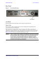
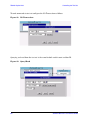
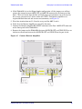
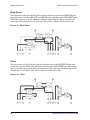
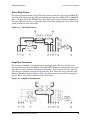
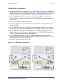
1
Agilent Technologies
Z5623A Option H83
User’s and Service Guide
Use this manual with the following documents:
PNA Series Network Analyzer On-line Help System
Application Note 1408-12
Manufacturing Part Number: Z5623-90070
Printed Date: December 2008
Supersede: February 2008
© Copyright 2004, 2006- 2008 Agilent Technologies, Inc. All rights reserved.
Warranty Statement
THE MATERIAL CONTAINED IN THIS DOCUMENT IS PROVIDED “AS IS,” AND IS SUBJECT
TO BEING CHANGED, WITHOUT NOTICE, IN FUTURE EDITIONS. FURTHER, TO THE
MAXIMUM EXTENT PERMITTED BY APPLICABLE LAW, AGILENT DISCLAIMS ALL
WARRANTIES, EITHER EXPRESS OR IMPLIED WITH REGARD TO THIS MANUAL AND
ANY INFORMATION CONTAINED HEREIN, INCLUDING BUT NOT LIMITED TO THE
IMPLIED WARRANTIES OF MERCHANTABILITY AND FITNESS FOR A PARTICULAR
PURPOSE. AGILENT SHALL NOT BE LIABLE FOR ERRORS OR FOR INCIDENTAL
OR CONSEQUENTIAL DAMAGES IN CONNECTION WITH THE FURNISHING, USE, OR
PERFORMANCE OF THIS DOCUMENT OR ANY INFORMATION CONTAINED HEREIN.
SHOULD AGILENT AND THE USER HAVE A SEPARATE WRITTEN AGREEMENT WITH
WARRANTY TERMS COVERING THE MATERIAL IN THIS DOCUMENT THAT CONFLICT
WITH THESE TERMS, THE WARRANTY TERMS IN THE SEPARATE AGREEMENT WILL
CONTROL.
DFARS/Restricted Rights Notice
If software is for use in the performance of a U.S. Government prime contract or
subcontract, Software is delivered and licensed as “Commercial computer software” as
defined in DFAR 252.227-7014 (June 1995), or as a “commercial item” as defined in FAR
2.101(a) or as “Restricted computer software” as defined in FAR 52.227-19 (June 1987) or
any equivalent agency regulation or contract clause. Use, duplication or disclosure of
Software is subject to Agilent Technologies’ standard commercial license terms, and
non-DOD Departments and Agencies of the U.S. Government will receive no greater than
Restricted Rights as defined in FAR 52.227-19(c)(1-2) (June 1987). U.S. Government users
will receive no greater than Limited Rights as defined in FAR 52.227-14 (June 1987) or
DFAR 252.227-7015 (b)(2) (November 1995), as applicable in any technical data.
ii
Z5623 H83 User’s and Service Guide
Safety Notes
The following safety notes are used throughout this document. Familiarize yourself with
each of these notes and its meaning before performing any of the procedures in this
document.
WARNING
Warning denotes a hazard. It calls attention to a procedure
which, if not correctly performed or adhered to, could result in
injury or loss of life. Do not proceed beyond a warning note
until the indicated conditions are fully understood and met.
CAUTION
Caution denotes a hazard. It calls attention to a procedure that, if not
correctly performed or adhered to, could result in damage to or
destruction of the instrument. Do not proceed beyond a caution sign
until the indicated conditions are fully understood and met.
Definitions
• Specifications describe the performance of parameters covered by the product warranty
(temperature –0 to 55 °C, unless otherwise noted.)
• Typical describes additional product performance information that is not covered by the
product warranty. It is performance beyond specification that 80% of the units exhibit
with a 95% confidence level over the temperature range 20 to 30 °C. Typical
performance does not include measurement uncertainty.
• Nominal values indicate expected performance or describe product performance that is
useful in the application of the product, but is not covered by the product warranty.
• Characteristic Performance describes performance parameter that the product is
expected to meet before it leaves the factory, but is not verified in the field and is not
covered by the product warranty. A characteristic includes the same guard bands as a
specification.
Z5623 H83 User’s and Service Guide
iii
iv
Z5623 H83 User’s and Service Guide
Contents
Z5623A Option H83
Description . . . . . . . . . . . . . . . . . . . . . . . . . . . . . . . . . . . . . . . . . . . . . . . . . . . . . . . . . . . . . . . . . . 2
Verifying the Shipment . . . . . . . . . . . . . . . . . . . . . . . . . . . . . . . . . . . . . . . . . . . . . . . . . . . . . . . . 3
General Information. . . . . . . . . . . . . . . . . . . . . . . . . . . . . . . . . . . . . . . . . . . . . . . . . . . . . . . . . . . 4
Video Feedthru . . . . . . . . . . . . . . . . . . . . . . . . . . . . . . . . . . . . . . . . . . . . . . . . . . . . . . . . . . . . . . . 5
Electrical Preparations . . . . . . . . . . . . . . . . . . . . . . . . . . . . . . . . . . . . . . . . . . . . . . . . . . . . . . . . 6
Environmental Preparations . . . . . . . . . . . . . . . . . . . . . . . . . . . . . . . . . . . . . . . . . . . . . . . . . . . . 8
Electrostatic Discharge Protection . . . . . . . . . . . . . . . . . . . . . . . . . . . . . . . . . . . . . . . . . . . . . . . 9
Test Set Familiarization. . . . . . . . . . . . . . . . . . . . . . . . . . . . . . . . . . . . . . . . . . . . . . . . . . . . . . . 10
Front Panel . . . . . . . . . . . . . . . . . . . . . . . . . . . . . . . . . . . . . . . . . . . . . . . . . . . . . . . . . . . . . . . 10
Power On Switch . . . . . . . . . . . . . . . . . . . . . . . . . . . . . . . . . . . . . . . . . . . . . . . . . . . . . . . . . 10
Power LED . . . . . . . . . . . . . . . . . . . . . . . . . . . . . . . . . . . . . . . . . . . . . . . . . . . . . . . . . . . . . . 10
RF Connectors . . . . . . . . . . . . . . . . . . . . . . . . . . . . . . . . . . . . . . . . . . . . . . . . . . . . . . . . . . . 10
Pulse Connector . . . . . . . . . . . . . . . . . . . . . . . . . . . . . . . . . . . . . . . . . . . . . . . . . . . . . . . . . . 10
Rear Panel . . . . . . . . . . . . . . . . . . . . . . . . . . . . . . . . . . . . . . . . . . . . . . . . . . . . . . . . . . . . . . . . 11
Line Module . . . . . . . . . . . . . . . . . . . . . . . . . . . . . . . . . . . . . . . . . . . . . . . . . . . . . . . . . . . . . 11
Power Cables . . . . . . . . . . . . . . . . . . . . . . . . . . . . . . . . . . . . . . . . . . . . . . . . . . . . . . . . . . . . 11
The Line Fuse . . . . . . . . . . . . . . . . . . . . . . . . . . . . . . . . . . . . . . . . . . . . . . . . . . . . . . . . . . . 12
Operation . . . . . . . . . . . . . . . . . . . . . . . . . . . . . . . . . . . . . . . . . . . . . . . . . . . . . . . . . . . . . . . . . . 13
System Setup . . . . . . . . . . . . . . . . . . . . . . . . . . . . . . . . . . . . . . . . . . . . . . . . . . . . . . . . . . . . . . . 16
Pulse Test Set Control Program . . . . . . . . . . . . . . . . . . . . . . . . . . . . . . . . . . . . . . . . . . . . . . . . 20
Getting Started . . . . . . . . . . . . . . . . . . . . . . . . . . . . . . . . . . . . . . . . . . . . . . . . . . . . . . . . . . . 20
Pulse Control Program Installation . . . . . . . . . . . . . . . . . . . . . . . . . . . . . . . . . . . . . . . . . . . . 21
Accessing the Program . . . . . . . . . . . . . . . . . . . . . . . . . . . . . . . . . . . . . . . . . . . . . . . . . . . . . . 24
Control Panel Features . . . . . . . . . . . . . . . . . . . . . . . . . . . . . . . . . . . . . . . . . . . . . . . . . . . . 26
Controlling the Test Set . . . . . . . . . . . . . . . . . . . . . . . . . . . . . . . . . . . . . . . . . . . . . . . . . . . . . . . 27
Commands . . . . . . . . . . . . . . . . . . . . . . . . . . . . . . . . . . . . . . . . . . . . . . . . . . . . . . . . . . . . . . . . 27
Typeface Key Conventions . . . . . . . . . . . . . . . . . . . . . . . . . . . . . . . . . . . . . . . . . . . . . . . . . . . 27
PNA Control . . . . . . . . . . . . . . . . . . . . . . . . . . . . . . . . . . . . . . . . . . . . . . . . . . . . . . . . . . . . . . 28
Addressing Directly. . . . . . . . . . . . . . . . . . . . . . . . . . . . . . . . . . . . . . . . . . . . . . . . . . . . . . . . . 30
RMB . . . . . . . . . . . . . . . . . . . . . . . . . . . . . . . . . . . . . . . . . . . . . . . . . . . . . . . . . . . . . . . . . . . 30
VEE . . . . . . . . . . . . . . . . . . . . . . . . . . . . . . . . . . . . . . . . . . . . . . . . . . . . . . . . . . . . . . . . . . . 31
Quick Basic . . . . . . . . . . . . . . . . . . . . . . . . . . . . . . . . . . . . . . . . . . . . . . . . . . . . . . . . . . . . . 33
National Instruments VISA . . . . . . . . . . . . . . . . . . . . . . . . . . . . . . . . . . . . . . . . . . . . . . . . 34
Parallel Port. . . . . . . . . . . . . . . . . . . . . . . . . . . . . . . . . . . . . . . . . . . . . . . . . . . . . . . . . . . . . . . 34
Direct Control . . . . . . . . . . . . . . . . . . . . . . . . . . . . . . . . . . . . . . . . . . . . . . . . . . . . . . . . . . . . . 36
Controlling the Switches. . . . . . . . . . . . . . . . . . . . . . . . . . . . . . . . . . . . . . . . . . . . . . . . . . . . . 36
Switch Indicators . . . . . . . . . . . . . . . . . . . . . . . . . . . . . . . . . . . . . . . . . . . . . . . . . . . . . . . . . . 36
Switch Indicator Function . . . . . . . . . . . . . . . . . . . . . . . . . . . . . . . . . . . . . . . . . . . . . . . . . . . 38
Controlling the Attenuators . . . . . . . . . . . . . . . . . . . . . . . . . . . . . . . . . . . . . . . . . . . . . . . . . . 39
Making High Power Measurements With Option H83 . . . . . . . . . . . . . . . . . . . . . . . . . . . . . . 42
Initial Setup . . . . . . . . . . . . . . . . . . . . . . . . . . . . . . . . . . . . . . . . . . . . . . . . . . . . . . . . . . . . . . 42
Determining Power Levels. . . . . . . . . . . . . . . . . . . . . . . . . . . . . . . . . . . . . . . . . . . . . . . . . . . . . 44
Selecting Power Ranges and Attenuator Settings . . . . . . . . . . . . . . . . . . . . . . . . . . . . . . . . . . 46
Additional Setup . . . . . . . . . . . . . . . . . . . . . . . . . . . . . . . . . . . . . . . . . . . . . . . . . . . . . . . . . . . 48
Final Setup and Response Calibration . . . . . . . . . . . . . . . . . . . . . . . . . . . . . . . . . . . . . . . . . 49
Test Set Internal Configurations. . . . . . . . . . . . . . . . . . . . . . . . . . . . . . . . . . . . . . . . . . . . . . . . 51
Bypass . . . . . . . . . . . . . . . . . . . . . . . . . . . . . . . . . . . . . . . . . . . . . . . . . . . . . . . . . . . . . . . . . . . 51
High Power . . . . . . . . . . . . . . . . . . . . . . . . . . . . . . . . . . . . . . . . . . . . . . . . . . . . . . . . . . . . . . . 52
Contents-1
Contents
Pulse . . . . . . . . . . . . . . . . . . . . . . . . . . . . . . . . . . . . . . . . . . . . . . . . . . . . . . . . . . . . . . . . . . . . .52
Pulse High Power . . . . . . . . . . . . . . . . . . . . . . . . . . . . . . . . . . . . . . . . . . . . . . . . . . . . . . . . . . .53
Amplifier Terminate. . . . . . . . . . . . . . . . . . . . . . . . . . . . . . . . . . . . . . . . . . . . . . . . . . . . . . . . .53
Specification. . . . . . . . . . . . . . . . . . . . . . . . . . . . . . . . . . . . . . . . . . . . . . . . . . . . . . . . . . . . . . . . .54
Pulsed RF PIN Switch Modulator . . . . . . . . . . . . . . . . . . . . . . . . . . . . . . . . . . . . . . . . . . . . . .54
E8362B Option H11 . . . . . . . . . . . . . . . . . . . . . . . . . . . . . . . . . . . . . . . . . . . . . . . . . . . . . . . . .54
Test Set Performance Verification . . . . . . . . . . . . . . . . . . . . . . . . . . . . . . . . . . . . . . . . . . . . . . .55
Equipment Required . . . . . . . . . . . . . . . . . . . . . . . . . . . . . . . . . . . . . . . . . . . . . . . . . . . . . . . .55
Procedure . . . . . . . . . . . . . . . . . . . . . . . . . . . . . . . . . . . . . . . . . . . . . . . . . . . . . . . . . . . . . . . . . . .56
CPLR Thru S-Parameters . . . . . . . . . . . . . . . . . . . . . . . . . . . . . . . . . . . . . . . . . . . . . . . . . . . .57
RCVR Port S-Parameters. . . . . . . . . . . . . . . . . . . . . . . . . . . . . . . . . . . . . . . . . . . . . . . . . . . . .58
On/Off Switch Ratio . . . . . . . . . . . . . . . . . . . . . . . . . . . . . . . . . . . . . . . . . . . . . . . . . . . . . . . . .59
Attenuator Settings . . . . . . . . . . . . . . . . . . . . . . . . . . . . . . . . . . . . . . . . . . . . . . . . . . . . . . . . .60
Rear Panel Termination Test. . . . . . . . . . . . . . . . . . . . . . . . . . . . . . . . . . . . . . . . . . . . . . . . . .61
Rise and Fall Time Test . . . . . . . . . . . . . . . . . . . . . . . . . . . . . . . . . . . . . . . . . . . . . . . . . . . . . .62
Replaceable Parts . . . . . . . . . . . . . . . . . . . . . . . . . . . . . . . . . . . . . . . . . . . . . . . . . . . . . . . . . . . .67
Safety and Regulatory Information
Introduction . . . . . . . . . . . . . . . . . . . . . . . . . . . . . . . . . . . . . . . . . . . . . . . . . . . . . . . . . . . . . . . . .70
Connector Care and Cleaning . . . . . . . . . . . . . . . . . . . . . . . . . . . . . . . . . . . . . . . . . . . . . . . . . . .70
Before Applying Power . . . . . . . . . . . . . . . . . . . . . . . . . . . . . . . . . . . . . . . . . . . . . . . . . . . . . . . .70
Declaration of Conformity . . . . . . . . . . . . . . . . . . . . . . . . . . . . . . . . . . . . . . . . . . . . . . . . . . . . . .70
Statement of Compliance . . . . . . . . . . . . . . . . . . . . . . . . . . . . . . . . . . . . . . . . . . . . . . . . . . . . . .70
Compliance with Canadian EMC Requirements . . . . . . . . . . . . . . . . . . . . . . . . . . . . . . . . . . .71
Compliance with German Noise Requirements . . . . . . . . . . . . . . . . . . . . . . . . . . . . . . . . . . . .71
Warnings . . . . . . . . . . . . . . . . . . . . . . . . . . . . . . . . . . . . . . . . . . . . . . . . . . . . . . . . . . . . . . . . . . .72
Cautions . . . . . . . . . . . . . . . . . . . . . . . . . . . . . . . . . . . . . . . . . . . . . . . . . . . . . . . . . . . . . . . . . . . .73
Instrument Markings . . . . . . . . . . . . . . . . . . . . . . . . . . . . . . . . . . . . . . . . . . . . . . . . . . . . . . . . .74
Agilent Support, Services, and Assistance . . . . . . . . . . . . . . . . . . . . . . . . . . . . . . . . . . . . . . . . .75
Service and Support Options . . . . . . . . . . . . . . . . . . . . . . . . . . . . . . . . . . . . . . . . . . . . . . . . . .75
Contacting Agilent . . . . . . . . . . . . . . . . . . . . . . . . . . . . . . . . . . . . . . . . . . . . . . . . . . . . . . . . . .75
Shipping Your Analyzer to Agilent for Service or Repair . . . . . . . . . . . . . . . . . . . . . . . . . . .75
Contents-2
Z5623A Option H83
Z5623A H83 User’s and Service Guide
1
Z5623A Option H83
Description
Description
The Agilent Z5623AH83 is a 2 GHz to 20 GHz dual directional pulse test set.
When connected to the E8362B Series Network Analyzer with Option H08 (Pulse) and
H11 (IF access) allows pulse measurements to be made from 2 GHz to 20 GHz for both the
forward and reverse parameters. The Z5623AH83 can be configured in many ways.
The Bypass configuration allows the E8362B Series Network Analyzer to be used from
10 MHz to 20 GHz depending on the analyzer. This mode bypasses the test sets internal
2 GHz to 20 GHz PIN modulator switch. In the Pulse mode the user can configure the test
set for their application needs, such as straight un-condition pulse measurements or
permit the insertion of high power amplifiers and other signal conditioning equipment.
This allows high power measurements at RF levels up to 20 Watts (+43 dBm) from 10 MHz
to 20 GHz. This document details a step by step procedure to configure the test set for high
power operation.
Control of the Agilent Z5623AH83 Dual Directional Pulse Test Set can be performed either
by GPIB or directly. Both methods control the Port 1 and 2 internal switches and
attenuators. Direct control requires the user to connect to two 37-pin D-Sub connectors
that are located on the rear panel. Both GPIB and direct control cannot be used
simultaneously. When used in the direct control mode the test sets front panel LCD
indicator may differ from the user setup.
High power configurations require that attenuators and isolators be connected to the test
ports and receivers to protect the E8362B. The Agilent E8362BH85 High Power
Configurable PNA Series Network Analyzer when ordered with the Option H08 and H11
can be used for high power pulse measurement applications. More information on the
setup and configuration can be found in the E8362B, E8363B and E8364B Option H85
User’s and Service Guide Supplement (E8364-90027).
Information regarding the PNA Option H08 and H11 can be found in the PNA online help
system.
The instrument is shipped from the factory with jumper cables installed on the front panel
in what is called the Shipped Configuration. Refer to Figure 10 on page 15.
Two high pass filters (Z5623-80027) have been provided with the Test Set. These filters are
used externally to eliminate video feed through from the PIN switch. The filters are used
for measurements in the range of 2 GHz to 20 GHz.
The pulse test set can be used from 400 MHz to 2 GHz but is not specified. No band pass
filters are provided for this frequency range. If low frequency pulse measurements are
required the user must supply the necessary high pass filter.
2
Z5623A H83 User’s and Service Guide
Z5623A Option H83
Verifying the Shipment
Verifying the Shipment
After the test set has been unpacked, keep the original packaging materials so they can be
used if you need to transport the instrument.
Check the items received against Table 1 to make sure you have received everything.
Inspect the test set and all accessories for any signs of damage that may have occurred
during shipment. If your test set or any accessories appear to be damaged or missing, refer
to “Agilent Support, Services, and Assistance” on page 75.
Table 1
Content List
Agilent
Part Number
Description
Qty
00909-60006
3.5 mm Male Termination
4
1250-0774
BNC short
2
1250-1788
Adapter sma(m) to sma(m)
2
5062-6681
Cable sma – 6 inches
2
5063-9226
Kit — Front Handles
1
5063-9232
Kit — Rack Mount
1
5064-3851
RCVR Jumper (rack mount)
2
5064-3852
Source Jumper (rack mount)
2
5064-3853
CPLR THRU Jumper (rack mount)
2
5064-3856
RCVR Jumper (bench mount)
2
5064-3857
Source Jumper (bench mount)
2
5064-3858
CPLR THRU Jumper (bench mount)
2
08720-20098
Front Panel Jumper (installed)
6
Z5623-10014
Pulse Test Set Control Programs disk
1
Z5623-80027
μ-Wave High Pass Filter 2 - 20 GHz
2
Z5623-60202
37-Pin D-SUB Jumper
2
Z5623-90070
User’s and Service Guide
1
Power Cord
See Figure 4 on page 7
1
Z5623A H83 User’s and Service Guide
3
Z5623A Option H83
General Information
General Information
Environmental:
Operating Temperature
Range
0 to 40 °C
Non-Operating
Temperature Range
–40 to 70 °C
Operating Humidity
Range
Maximum relative humidity 80% for temperatures up to 31 °C
decreasing linearly to 50% relative humidity at 40 °C (unless
specified otherwise).
Non-Operating Humidity
Range
Maximum relative humidity 90% for temperatures up to 65 °C
(noncondensing).
Operating Altitude
3000 meters (9840 ft)
Non-Operating Altitude
15,240 meters (50,000 ft)
EMC
Meets the conducted and radiated interference and immunity
requirements of IEC/EN 61326-1. Meets radiated emission
requirements of CISPR Pub 11/1997 Group 1 Class A.
Indoor/Outdoor Use
Indoor Use (unless specified otherwise)
This product is designed for use in INSTALLATION CATEGORY
II and POLLUTION DEGREE 2, per IEC 61010-1 Second
Edition and 664 respectively.
Power Requirements:
Frequency
50 to 60 Hz
Voltage
100/120 VAC
220/240VAC
Power
30 Watts
40 Watts
Weights and Dimensions:
4
Net Weight
9.1 kg (20 lb.)
Dimensions
Height: 9 cm (3.54 in)
Width: 42.5 cm (16.7 in)
Depth: 50 cm (19.7 in)
Z5623A H83 User’s and Service Guide
Z5623A Option H83
Video Feedthru
Video Feedthru
Video leakage refers to the spurious signals present at the RF ports of the switch when it is
switched without an RF signal present. Refer to Figure 1. These signals arise from the
waveforms generated by the switch driver and, in particular, from the leading edge voltage
spike required for high speed switching of PIN diodes. When measured into a 50 Ω system,
the magnitude of the video leakage can be as much as several volts. The frequency content
is concentrated in the band below 250 MHz, although measurable levels can be observed as
high as several GHz. The magnitude of the video leakage can be reduced significantly by
adding a high pass filter in the RF path Pulse Out to Filter In. Refer to Figure 2. The
picture below shows the leading and trailing edges of video feedthru.
Figure 1
Video Filter
Figure 2
Video Filter and Parts
5062-6681
1250-1788
Z5623-80027
Z5623A H83 User’s and Service Guide
5
Z5623A Option H83
Electrical Preparations
Electrical Preparations
1. Ensure that the “Power Requirements:” on page 4 are met.
2. Verify that the power cable is not damaged and that the power source outlet provides a
protective earth ground contact. Note that Figure 3 depicts only one type of power
source outlet. Refer to Figure 4 to see the different types of power cord plugs that can be
used with your test set.
Cables are available in different lengths. For descriptions and part numbers of cables
other than those described in Figure 4, Refer to “Contacting Agilent” on page 75.
3. If this product is to be powered by autotransformer, make sure the common terminal is
connected to the neutral (grounded) side of the ac power supply.
Figure 3
Protective Earth Ground
WARNING
This is a Safety Class I product (provided with a protective earthing
ground incorporated in the power cord). The mains plug shall only
be inserted into a socket outlet provided with a protective earth
contact. Any interruption of the protective conductor, inside or
outside the instrument, is likely to make the instrument dangerous.
Intentional interruption of the protective conductor is prohibited.
6
Z5623A H83 User’s and Service Guide
Z5623A Option H83
Figure 4
Electrical Preparations
Power Cables
a
Plug Type
250V
Cable
Part
Number
Plug b
Length
Description cm (in.)
Cable
Color
8120-8705
Straight
BS 1363A
229 (90)
Mint Gray
8120-8709
90
229 (90)
Mint Gray
8120-1369
Straight
AS 3112
210 (79)
Gray
8120-0696
90
200 (78)
Gray
8120-1378
Straight
NEMA 5-15P
203 (80)
Jade Gray
8120-1521
90
203 (80)
Jade Gray
8120-4753
Straight
NEMA 5-15P
229 (90)
Gray
8120-4754
90
229 (90)
Gray
8120-1689
Straight
CEE 7/VII
200 (78)
Mint Gray
8120-1692
90
200 (78)
Mint Gray
8120-2104
Straight
SEV Type 12
200 (78)
Gray
8120-2296
90
200 (78)
Gray
8120-2956
Straight
SR 107-2-D
200 (78)
Gray
8120-2957
90
200 (78)
Gray
8120-4211
Straight
IEC 83-B1
200 (78)
Mint Gray
8120-4600
90
200 (78)
Mint Gray
8120-5182
Straight
SI 32
200 (78)
Jade Gray
8120-5181
90
200 (78)
Jade Gray
E
L
N
250V
E
L
N
125V
E
N
L
125V
For Use
in Country
Option 900
United Kingdom, Hong
Kong, Cyprus, Nigeria,
Singapore, Zimbabwe
Option 901
Argentina, Australia,
New Zealand, Mainland
China
Option 903
United States, Canada,
Brazil, Colombia,
Mexico,Philippines,
Saudi Arabia, Taiwan
Option 918
Japan
E
N
L
250V
E
N
L
230V
Option 902
Continental Europe,
Central African Republic,
United Arab Republic
Option 906
Switzerland
E
L
N
220V
N
L
Option 912
Denmark
E
250V
Option 917
South Africa, India
E
L
N
250V
Option 919
Israel
E
N
L
a. E =earth ground, L = line, and N = neutral.
b. Plug identifier numbers describe the plug only. The Agilent Technologies part number is for the complete cable assembly.
Z5623A H83 User’s and Service Guide
7
Z5623A Option H83
Environmental Preparations
Environmental Preparations
1. Ensure that the “Power Requirements:” on page 4 are met.
2. If you are installing the test set into a cabinet, ensure there are at least two inches of
clearance around the sides and back of the test set and the system cabinet. See
Figure 5. The convection into and out of the test set must not be restricted. The ambient
temperature (outside the cabinet) must be less than the maximum operating
temperature of the test set by 4 °C for every 100 watts dissipated in the cabinet.
Figure 5
CAUTION
8
Ventilation Clearance Requirements
If the total power dissipated in the cabinet is greater than 800 watts,
forced convection must be used.
Z5623A H83 User’s and Service Guide
Z5623A Option H83
Electrostatic Discharge Protection
Electrostatic Discharge Protection
Protection against electrostatic discharge (ESD) is essential while removing assemblies
from or connecting cables to the network analyzer. Static electricity can build up on your
body and can easily damage sensitive internal circuit elements when discharged. Static
discharges too small to be felt can cause permanent damage. To prevent damage to the
instrument:
• always have a grounded, conductive table mat (9300-0797) in front of your test
equipment.
• always wear a grounded wrist strap (9300-1367) with grounding cord (9300-0980),
connected to a grounded conductive table mat, having a 1 MΩ resistor in series with it,
when handling components and assemblies or when making connections.
• always wear a heel strap (9300-1126) when working in an area with a conductive floor.
If you are uncertain about the conductivity of your floor, wear a heel strap.
• always ground yourself before you clean, inspect, or make a connection to a
static-sensitive device or test port. You can, for example, grasp the grounded outer shell
of the test port or cable connector briefly.
• always ground the center conductor of a test cable before making a connection to the
analyzer test port or other static-sensitive device. This can be done as follows:
1. Connect a short (from your calibration kit) to one end of the cable to short the center
conductor to the outer conductor.
2. While wearing a grounded wrist strap, grasp the outer shell of the cable connector.
3. Connect the other end of the cable to the test port and remove the short from the
cable.
Figure 5-2 ESD Protection Setup
Z5623A H83 User’s and Service Guide
9
Z5623A Option H83
Test Set Familiarization
Test Set Familiarization
This section familiarizes the user with various front and rear panel features of the test set.
Front Panel
Figure 6
Front Panel Features
BNC Short (1250-0774)
Attached to Pulse In
Power On Switch
The Power On switch turns the AC power to the test set on and off. The switch is located at
the bottom left corner of the front panel.
The switch disconnects the mains circuits from the mains supply after the EMC filters and
before other parts of the instrument.
Power LED
The power LED is illuminated when the power switch is in the on (1) position.
RF Connectors
All of the RF connectors are 50 Ω APC 3.5 mm connectors.
Pulse Connector
The pulse input connector is a 50 Ω ΒΝC female connectors.
10
Z5623A H83 User’s and Service Guide
Z5623A Option H83
Test Set Familiarization
Rear Panel
Figure 7
Rear Panel Features
Line Module
Line Module
The line module contains the power cable receptacle and the line fuse.
Power Cables
The line power cable is supplied in one of several configurations, depending on the
destination of the original shipment.
Each instrument is equipped with a three-wire power cable. When connected to an
appropriate ac power receptacle, this cable grounds the instrument chassis. The type of
power cable shipped with each instrument depends on the country of destination. See
Figure 4 on page 7 for the part numbers of these power cables.
WARNING
This is a Safety Class I product (provided with a protective earthing
ground incorporated in the power cord). The mains plug shall only
be inserted in a socket outlet provided with a protective earth
contact. Any interruption of the protective conductor, inside or
outside the instrument, is likely to make the instrument dangerous.
Intentional interruption is prohibited.
Z5623A H83 User’s and Service Guide
11
Z5623A Option H83
Test Set Familiarization
The Line Fuse
The line fuse (F 3 A/250 V, 2110-0780) and a spare reside within the line module. Figure 8
illustrates where the fuses are and how to access them.
Figure 8
12
Location of Line Fuses
Z5623A H83 User’s and Service Guide
Z5623A Option H83
Operation
Operation
The Agilent Z5623AH83 Dual Directional Pulse Test Set can be configured differently for
many applications. Included in this document are three typical configurations:
• Figure 10, “Shipped Configuration.”
• Figure 12, “High Power Forward Direction.”
• Figure 13, “High Power Dual Directional.”
NOTE
The internal firmware of the PNA has not been modified for this test set
option. The power levels indicated on the Agilent E8363B and E8364B may
differ depending on the user configuration that is chosen.
Refer to the configuration diagrams for external component connections and/or operating
constraints when utilizing the high power capability of the Agilent Z5623AH83 Dual
Directional Pulse Test Set. External components are not supplied with this option.
When using the Agilent E8362B Series Network Analyzer with Z5623AH83 Dual
Directional Pulse Test Set in the bypass or the high power configuration, the PNA
Frequency Offset mode (Option 080) and External R1 (Option 081) must be activated. This
will ensure phase lock and allow R1 and R2 to receive the new reference power levels from
the amplifiers. Refer to Table 3 on page 14.
CAUTION
The Z5623AH83 is equipped with reference channel attenuators. These
attenuators reduce the RF power to the PNA R1 and R2 receiver ports. The
test set attenuators can be set from 0 to 60 dB in 10 dB steps. The
recommended power levels to the PNA R1 and R2 receiver ports is –15 dBm.
Refer to your PNA specifications to optimize power levels to the receiver
ports.
The PNA Option 016, Receiver Step Attenuators, reduces the power to the A
and B receivers. The A and B maximum attenuator setting is 35 dB. Power
measurements to Test Ports 1 and 2 above +35 dBm will require additional
attenuation. Add the appropriate amount of attenuation that will keep the
coupler arm output power below –15 dBm. Refer to Table 3 on page 14.
CAUTION
Hot Switching is not allowed with the Z5623AH83 when making high power
measurements or damage to the switch will occur. Hot Switching is the
condition when the internal switch or switches are set to a position for
making high power measurements, and then set to another position without
reducing the power. The maximum power that the switches are allowed to
switch states is +20 dBm.
Z5623A H83 User’s and Service Guide
13
Z5623A Option H83
CAUTION
Table 3
Operation
Prior to powering-up the booster amplifier, it is highly recommended that the
user verify the RF power levels seen by the various elements of the test setup.
At high power levels a mistake could permanently damage the instrument.
Refer to Table 3 on page 14.
Power Levels
Test Setup
Power Level
Maximum Z5623AH83 RF Power Levels to Access Ports:
SOURCE IN
+20 dbm
RCVR R1 OUT, RCVR R2 OUT
+20 dBm
CPLR THRU, CPLR IN, AMP IN
+43 dBm @ 10 MHz to 20 GHz
AMP OUT, SOURCE OUT
+30 dbm
FILTER IN
+30 dBm (dependent on filter)
PULSE OUT
+20 dbm (dependent on filter)
AMP 1 IN TERM, AMP 2 IN TERM
+30 dBm
AMP 1 OUT TERM, AMP 2 OUT TERM
+30 dbm
Maximum PNA RF Power Levels to Access and Test Ports:
Max Recommended RF Level at A/B/R1/R2 Receivers
– 15 dbm
Damage Level at A/B/R1/R2 Receivers
+15 dbm
Max Recommended RF Level at Port 1, 2 Source
+0 dBm
Damage Level to Port 1, 2 SOURCE OUT
+20 dBm
Max Level to Port 1, 2 Test Ports
+20 dBm
NOTE
Refer to your PNA specifications to optimize the power levels in the receivers.
NOTE
We recommend that you do not operate components near damage or
maximum levels. The power levels should be kept at less than 3 dB,
preferably 6 dB, below damage and maximum levels.
14
Z5623A H83 User’s and Service Guide
Z5623A Option H83
Figure 9
Operation
Maximum Power Levels
J4
J3
+30 dBm
Port 1 Side
2
1
4
1
2
1
SW2
SW3
4
3
3
2
SW1
4
3
ATN1
60 dB
16 dB
SW7
CPLR1
SOURCE FILTER PULSE
IN
IN
OUT
+20 dBm
+20 dBm
+30 dBm
AMP
OUT
PULSE 1
IN
AMP SOURCE CPLR
IN
OUT
IN
10/20/30
CPLR
THRU
RCVR
R1 OUT
+20 dBm
5 volts DC
10K Ohm
+30 dBm
+30 dBm
+43 dBm @ 10 MHz to 20 GHz
J2
J1
+30 dBm
Port 2 Side
2
1
4
3
2
1
SW5
SW6
3
4
2
1
SW4
ATN2
60 dB
3
4
16 dB
SW8
10/20/30
RCVR
R2 OUT
CPLR2
CPLR
THRU
CPLR SOURCE AMP
IN
OUT
IN
AMP
OUT
+20 dBm
+30 dBm +30 dBm
PULSE 2
IN
5 volts DC
10K Ohm
PULSE FILTER SOURCE
OUT
IN
IN
+20 dBm
+20 dBm
+30 dBm
+43 dBm @ 10 MHz to 20 GHz
Figure 10
Shipped Configuration
BNC Short (1250-0774)
Attached to Pulse In
Z5623A H83 User’s and Service Guide
15
Z5623A Option H83
System Setup
System Setup
Figure 11 on page 17 shows the setup configuration of the Z5623AH83 Dual Directional
Pulse Test Set and how it should be configured with the PNA and the Pulse Pattern
Generators.
1. Connect the following RF Cables:
• Connect RF Cable (5064-3852 - rack mount) or (5064-3857 - bench mount) from the
Test Set RCVR R1 or R2 to the PNA RCVR R1 or R2 IN.
• Connect RF Cable (5064-3851 - rack mount) or (5064-3856 - bench mount) from the
Test Set SOURCE IN to the PNA SOURCE OUT (Ports 1 & 2).
• Connect RF Cable (5064-3853 - rack mount) or (5064-3858 - bench mount) from the
Test Set CPLR THUR to the PNA CPLR THUR (Ports 1 & 2).
NOTE
The test set rear panel connections are not shown in Figure 11 on page 17.
2. Connect the external 50 Ω loads (00909-60006) on Test Set RF Ports to J1, J2, J3,
and J4.
3. Connect the test set’s 37-Pin D-SUB jumpers (Z5623-60202) to the rear panel Port 1 and
Port 2 connectors for GPIB and parallel control.
4. Connect the GPIB cable from the PNA, Test Set and Pulse Pattern Generators. (These
cables are not supplied).
5. Connect a BNC cable for the 10 MHz Reference between the PNA and the Pulse Pattern
Generators. (These cables are not supplied).
6. Connect the four BNC cables from each Pulse Pattern Generators Output 1 and 2 to the
PNA rear panel IF Inputs. (These cables are not supplied).
7. Connect two BNC cables from the Test sets PULSE 1 and 2 IN to the Pulse Pattern
Generator. (These cables are not supplied).
16
Z5623A H83 User’s and Service Guide
Z5623A Option H83
Figure 11
System Setup
System Setup Configuration
5064-3853 or
5064-3858
5064-3851 or
5064-3856
5064-3852 or
5064-3857
Z5623A H83 User’s and Service Guide
17
Z5623A Option H83
System Setup
In the following diagrams a high power isolator or attenuator must be inserted at the front
panel CPLR IN and SOURCE OUT to protect the internal test set modulator PIN switch
and the PNA solid state transfer switch (30 dB isolation recommended), or if reverse
isolation of the amplifier is less than 30 dB. Maximum power into the modulator PIN
switch is 20 dBm for both forward and reverse directions. Optimum power level to all
receivers is –15 dBm.
• Insert attenuators (A, B, R1 and R2 ports) to reduce power to the receivers accordingly.
• Set the initial instrument state to –65 dBm test port power level to reduce the risk of
damage when powering on the unit.
• The recommended sweep mode is [STEP].
• Frequency Offset mode must be On and the R1 reference channel should be
set to External.
Figure 12
18
High Power Forward Direction
Z5623A H83 User’s and Service Guide
Z5623A Option H83
Figure 13
System Setup
High Power Dual Directional
Z5623A H83 User’s and Service Guide
19
Z5623A Option H83
Pulse Test Set Control Program
Pulse Test Set Control Program
Getting Started
Your Z5623A Pulse Test Set, comes with a Pulse Control Program disk,
(Z5623-10014, Disk 1 of 1). This disk is in a DOS high density format and can be inserted
directly into the PNA disk drive. Your PNA must have revision 6.0 PNA firmware and XP
operating system installed so that the Pulse Test Set Control Program can be installed.
1. You can verify your PNA operating system by navigating to the PNA desktop. Rightclick the My Computer icon. A drop-down menu will appear. Refer to Figure 14.
Figure 14
Desk Top Properties
2. Select Properties in the drop-down menu. The System Properties will appear. Refer to
Figure 15.
Figure 15
XP OS
3. If your analyzer does not have the XP OS stop, you will need to upgrade the PNA with
the N8990A. This option will install a new CPU and the XP operating system.
20
Z5623A H83 User’s and Service Guide
Z5623A Option H83
Pulse Test Set Control Program
Pulse Control Program Installation
The Pulse Control Program disk has the file to control the Pulse Test Sets. It is found by
navigating to the A:\ (floppy drive) after the Control Program diskette has been inserted
into the PNA disk drive. Refer to Figure 16.
Figure 16
Disk Program Files
1. Using Windows Explorer, navigate to the C:/Program Files directory to verify that a
“temp” directory exists. If not, create one by right-clicking within the Program Files
folder then select New > Folder and name it “temp”. Once the temp directory is created
or located, insert the Pulse Control Program disk into the PNA disk drive. Copy the
desired file listed above into the temp folder from the A:\(floppy drive) to the
C:\Program Files\temp folder. Refer to Figure 17.
Figure 17
Temp Folder
2. The file copied into the temp directory must be renamed to function. The file has an
underscore “_” between Control_msi. Replace the underscore with a period “.” Highlight
the file name, right click and select rename.
Z5623A H83 User’s and Service Guide
21
Z5623A Option H83
Pulse Test Set Control Program
3. Once the file has been renamed, double-click on the file to start the installation. The
Setup Wizard will appear in the display.
4. Press Next. The Selection Installation folder will appear. Refer to Figure 18.
Figure 18
Installation Start
5. Press Next for default or to modify where to install the folder. Refer to Figure 19.
Figure 19
22
Folder Selection
Z5623A H83 User’s and Service Guide
Z5623A Option H83
Pulse Test Set Control Program
6. Press Next to confirm the installation. Refer to Figure 20.
Figure 20
Confirm Installation
7. Press Close to complete the installation. Refer to Figure 21.
Figure 21
Installation Complete
Z5623A H83 User’s and Service Guide
23
Z5623A Option H83
Pulse Test Set Control Program
Accessing the Program
The program installed will be located in its own file folder:
C:\Program Files\Agilent\Agilent PNA Pulse Test Set Control
1. Locate the file directory. Refer to Figure 22.
2. Select the Agilent PNA Pulse Test Set Control folder. Refer to Figure 22.
Figure 22
Locate the Folder
3. Double-click PulseTestSetControl.exe file. Refer to Figure 23.
Figure 23
24
PulseTestSetControl.exe
Z5623A H83 User’s and Service Guide
Z5623A Option H83
Pulse Test Set Control Program
Once the file has been executed the Agilent Pulse Test Set Control panel will appear. The
control panel shown in Figure 24 is for Option H86 that has the forward direction (Port 1)
only and therefore, the Port 2 controls are not selectable. For the dual direction models
both port controls will be active.
Figure 24
Control Panel
Z5623A H83 User’s and Service Guide
25
Z5623A Option H83
Pulse Test Set Control Program
Control Panel Features
The control panel is used to set the operation mode of the test set to the user’s
requirements.
These features are listed in the user manual for the Pulse Test Set.
As outlined in the manual switching between Bypass/Pulse Modes to High Power Modes
can damage the test set and PNA if care is not taken.
Test Mode of Operation
• Bypass Mode - PNA in its normal operation
• High Power Mode - Allows the user to insert source amplifiers
• Pulse Mode - Accesses the pin switch modulator
• Pulse High Power Mode - Accesses the pin switch modulator and allows the user to
insert amplifiers
Reference Attenuator
• Allows the user to select between 0 to 60 dB in 10 dB steps the amount of attenuation to
the reference channel for high power applications.
GPIB Address
• The address of the Pulse Test Set. Default is 712. Only the last two digits are required.
26
Z5623A H83 User’s and Service Guide
Z5623A Option H83
Controlling the Test Set
Controlling the Test Set
The Agilent Z5623AH83 is considered a “slave” instrument. A Controller must be used to
control the test set. There are four ways to control the test set:
• The PNA can be used as the controller to talk to the test set over the GPIB.
• A Controller can directly talk to the test set over the GPIB.
• The Parallel port can be used to set the test set.
• Direct control access to the internal switches and attenuators via open collector lines
to ground the input lines.
Commands
As mentioned before, the test set can be controlled in four ways. The first two involve the
use of a separate computer. The third way uses parallel port manually. The fourth control
method uses direct access from two rear panel 37 pin D-Sub connectors.
NOTE
The 37 pin D-Sub jumpers (Z5623-60202) must be attached to the test sets
Port 1 and 2 rear panel direct access connectors for the GPIB and parallel
port commands to work. These connectors are not connected to the test set
when they are shipped.
Typeface Key Conventions
The following key conventions are used throughout this document.
• [HARDKEYS] are labeled front panel keys.
• SOFTKEYS are unlabeled key whose function is indicated on the instrument display.
Z5623A H83 User’s and Service Guide
27
Z5623A Option H83
Controlling the Test Set
PNA Control
Write the GPIB commands from the PNA directly to the Z5623AH83 test set GPIB port
located on the rear panel. The following example assumes that the address of the test set is
set to 12. Be sure to use an ending semi-colon.
The PNA must be setup as the Controller first.
1. Select System > Configure > SICL/GPIB > System Controller. Press OK and close the
window.
Figure 25
28
SICL/GPIB
Z5623A H83 User’s and Service Guide
Z5623A Option H83
Controlling the Test Set
2. Launch the Measurement & Automation icon located on the PNA desk top.
3. Expand Devices and Interfaces.
4. Right click on GPIB0 (AT-GPIB/TNT) and select Interactive control. When the new
window appears at the prompt type the following:
: ibdev (This command sets up the PNA GPIB to talk to the Z5623AH83 test set)
enter board index: 0
enter primary address: 12
enter secondary address: 0
enter timeout: 0
enter 'EOI on last byte' flag: 1
ibwrt:"command$;" (Command$ is the string the user would get from the table.
Figure 26
Interactive Control
Z5623A H83 User’s and Service Guide
29
Z5623A Option H83
Controlling the Test Set
Addressing Directly
Write GPIB commands from the controller to write commands directly to the Z5623AH83
test set GPIB port located on the rear panel. The following RMB example assumes that the
address of the test set is set to 712.
RMB
OUTPUT 712;"command$;"
To query and read from the Z5623AH83 test set, the user needs to send two commands.
The first queries the test set for an individual switch count, and the second reads the data
as a string. Be sure to use an ending semi-colon. See your manual regarding details for
switching the identifier.
OUTPUT 712;"sw10?;"!Query test set for switch 10
ENTER 712;"Count$;" !Read switch 10 Count
To query and read from the Z5623AH83 test set ID, the user needs to send two commands.
The first queries the test set for an ID, and the second reads the data as a string. See your
manual for details for “ID Identifier read.”
OUTPUT 712;"idn?;"!Query test set for ID
ENTER 712;"Name$;"!Read test set ID
30
Z5623A H83 User’s and Service Guide
Z5623A Option H83
Controlling the Test Set
VEE
When using VEE be sure the Direct I/O is set as follows. This is also the default Direct I/O
settings.
Figure 27
Direct I\O
Z5623A H83 User’s and Service Guide
31
Z5623A Option H83
Controlling the Test Set
To send commands to test set configure the I/O Transaction as follows.
Figure 28
I/O Transaction
Querying and read from the test set is the same for both switch count and box ID.
Figure 29
32
Query/Read
Z5623A H83 User’s and Service Guide
Z5623A Option H83
Controlling the Test Set
Quick Basic
If you are using Quick Basic or Visual Basic, be sure to disable EOI and EOL before
sending commands to the test set. Including the semicolon in program commands will not
ensure that these commands are disabled as would be the case in HP Basic/RMB. When
using the 82335 GPIB Interface and Visual Basic, use the following commands to disable
EOI and EOL, send the necessary data to the test set, and re-enable EOI and EOL.
NOTE
Be sure to re-enable EOI and EOL before sending data to another
instrument.
Write Commands
GpibEoi(hGpib;7,0) 'disable EOI
GpibEol(hGpib;7, "",0) 'disable EOL
GpibOutputs(hGpib;712,info$,length%) 'send command to test set.
GpibEol(hGpib;7,chr$(13)+chr$(10),2) 're-enable EOL and set to
chr$(13)+chr$(10)
GpibEoi(hGpib;7,1,) 're-enable EOI where hGpib specifies the handle
returned by GpibOpen
Read Commands
info$ = "sw10?" 'query sw10 for switch count
length% = len(info$) 'length of command
max.len% =10 'max length data form idn? or swxx? function
infi$ = space$(max.len%)
GpibEoi(hGpib;7,0) 'disable EOI
GpibEol(hGpib;7, "",0) 'disable EOL
GpibOutputs(hGpib%,712,info$,length%) 'send query command to tests
set.
GpibEnters(hGpib%,712,infi$,max.len%) 'get data from tests set.
GpibEol(hGpib;7,chr$(13)+chr$(10),2) 're-enable EOL
GpibEoi(hGpib;7,1,) 're-enable EOI
Z5623A H83 User’s and Service Guide
33
Z5623A Option H83
Controlling the Test Set
National Instruments VISA
If you are using National Instruments VISA, be sure to set the variables as follows:
VI_ATTR_SEND_END_ENVI = FALSE ‘ This specifies whether to assert END during the
transfer of the last byte of the buffer.
VI_ATTR_TERMCHAR = 0x0A ‘ This is the termination character. When the termination
character is read and VI_ATTR_TERMCHAR_EN is enabled during a read operation, the
read operation terminates.
VI_ATTR_TERMCHAR_EN = VI_TRUE ‘ This is a flag that determines whether the read
operation should terminate when a termination character is received.
VI_ATTR_SUPPRESS_END_EN = VI_FALSE ‘ This specifies whether to suppress the
END bit termination. If this attribute is set to VI_TRUE, than the END bit does not
terminate read operations. If this attribute is set to VI_FALSE, than the END bit
terminates read operations.
Write Commands:
Append all commands with \n. For example; *rst\n
Read Commands:
The test set returns data terminated by \r\n. For example the query sw10?\n returns
00000010\r\n.
Parallel Port
The third way is used by the service center or during production to verify the port path
connections. This uses the parallel port on the rear panel of the Z5623AH83. This method
uses an 8722ES Network Analyzers Parallel port to control the test set. The following
example assumes that the address of the network analyzer is set to 16. Be sure to use an
ending semi-colon.
OUTPUT 716;"PARALGPIO" (Sets the parallel port for GPIO function).
OUTPUT 716;"PARAOUT[D]; (Programs all GPIO output bits (0 to 256) at once).
34
Z5623A H83 User’s and Service Guide
Z5623A Option H83
Table 4
Controlling the Test Set
GPIB and Parallel Commands
GPIB
Description
LCD Display
Parallel
Decimal
A100
RCVR R1 Attenuator 0 dB
A00
00000000
0
A110
RCVR R1 Attenuator 10 dB
A10
00000001
1
A120
RCVR R1 Attenuator 20 dB
A20
00000010
2
A130
RCVR R1 Attenuator 30 dB
A30
00000011
3
A140
RCVR R1 Attenuator 40 dB
A40
00000100
4
A150
RCVR R1 Attenuator 50 dB
A50
00000101
5
A160
RCVR R1 Attenuator 60 dB
A60
00000110
6
A200
RCVR R2 Attenuator 0 dB
A00
00000111
7
A210
RCVR R2 Attenuator 10 dB
A10
00001000
8
A220
RCVR R2 Attenuator 20 dB
A20
00001001
9
A230
RCVR R2 Attenuator 30 dB
A30
00001010
10
A240
RCVR R2 Attenuator 40 dB
A40
00001011
11
A250
RCVR R2 Attenuator 50 dB
A50
00001101
12
A260
RCVR R2 Attenuator 60 dB
A60
00001110
13
P1B
Port 1 Bypass Mode
P1 Bypass Axx
00001110
14
P1HPB
Port 1 High Power Mode
P1 HP Bypass Axx
00001111
15
P1HPP
Port 1 High Power Pulse Mode
P1 HP Pulse Axx
00010000
16
P1P
Port 1 Pulse Mode
P1 Pulse Axx
00010001
17
P2B
Port 2 Bypass Mode
P2 Bypass Axx
00010010
18
P2HPB
Port 2 High Power Mode
P2 HP Bypass Axx
00010011
19
P2HPP
Port 2 High Power Pulse Mode
P2 HP Pulse Axx
00010100
20
P2P
Port 2 Pulse Mode
P2 Pulse Axx
00010101
21
*RST
Reset (Port 1 and 2 Bypass Mode)
P1 Bypass A00
P2 Bypass A00
00010110
22
Display
IDN?
Description (GPIB)
Z5623AH83D
Read Test Set ID
ERR: invalid command
Non GPIB or Parallel Command Sent
Z5623A H83 User’s and Service Guide
35
Z5623A Option H83
Controlling the Test Set
Direct Control
The fourth method to control the test set uses the Port 1 and Port 2, 37 pin D-Sub
connectors located on the rear panel. Removing the jumper connectors (Z5623-60202) will
allow the user to control the internal switches and attenuators. Refer to Table 5 on page 40
which shows the pinout and function for Port 1 and Port 2.
NOTE
LCD indicator is only valid when the test set is used in control methods; PNA,
Controller, and Parallel. Direct control does not change the LCD indicator
when either the switches or attenuators are repositioned.
Controlling the Switches
Control of the internal switches directly, is provided from the 37 pin D-Sub connector and
can be done in two ways.
• TTL
• Open Collector
The TTL input allows the user independent switch position control by either a low (0) or
high (1). The TTL voltage is 0 or 5 volts. The Figure 30 on page 37. The 37 Pin D-Sub
connector shows the rear panel input/output configuration for Port 1. Port 2 is identical to
Port 1 but where SW1 is replace by SW4, SW2 is replace by SW5, SW3 is replace by SW6
on the RF block diagram. Pins 5, 12, 22 are the TTL input pins. Pin 5 controls SW1 or
SW4, pin 12 controls SW3 or SW6, and pin 22 controls SW2 or SW5.
The Open Collector inputs allows the user to control a switch position by grounding either
the A (AD) or B (BD) dive input lines for each switch. Only one of these two input lines can
be grounded at any given moment. Recommended is break before making when the input
line position changes. Refer to Figure 30. The 37 Pin D-Sub connector shows the rear panel
input/output configuration for port 1. Port 2 is identical to port 1 but where SW1 is replace
by SW4, SW2 is replace by SW5, SW3 is replace by SW6 on the RF block diagram. Pins
(1,2), (8,9), and (25,26) are the A and B drives input pins. Pins 1, 2 control SW1 or SW4,
pins 8, 9 control SW3 or SW6, and pins 25, 26 control SW2 or SW5.
Switch Indicators
The internal switch positions can be read only when used in the Direct Control method. A
switch position can be read by either a low (0) or high (1) on the A (AI) or B (BI) indicator
lines. The voltage is either 0 or 5 volts depending on the switch position. Low (0) indicates
disabled, and high (1) indicates enabled. Figure 30 shows the rear panel input/output
configuration for port 1. Port 2 is identical to port 1 but where SW1 is replace by SW4, SW2
is replace by SW5, SW3 is replace by SW6 on the RF block diagram. Pins (3,4), (10,11), and
(23,24) are the A and B indicator output pins. Pins 3, 4 indicate SW1 or SW4 position, pins
10, 11 indicate SW3 or SW6 position, and pins 23, 24 indicate SW2 or SW5 position.
Figure 31 on page 37 shows how each switch is configured.
36
Z5623A H83 User’s and Service Guide
Z5623A Option H83
Figure 30
37 Pin D-Sub Connector
Figure 31
Switch Connection
Z5623A H83 User’s and Service Guide
Controlling the Test Set
37
Z5623A Option H83
Controlling the Test Set
Switch Indicator Function
The 87222C is set to the A or B Position. See Table 6 on page 41, Switch Indicator Voltages
for Test Set Modes. When the switch is set to the A position the Indicator Common is
connected, completing the A Indicator path. The 21 VDC connected to the Indicator
Common is connected to ground by two resistors (30 kΩ and 10 kΩ). The Position A and B
Indicators have independent 10 kΩ resistors to ground. The measured voltage from
Position A Indicator to ground is approximately 5 Volts VDC and the Position B Indicator
will measure 0 Volts. When the switch is set to Position B, the Indicator common is
connected. Measuring the voltage from Position B Indicator to ground will measure
approximately 5 Volts VDC and the A indicator will measure 0 Volts.
Example 1 A Indicator Position Connected
•
•
•
•
•
•
•
•
Resistance Indicator Common in a connected path = 40 kΩ
Resistance between the Indicator Common and Position A when connected = 30 kΩ
Resistance between Position A and ground = 10 kΩ
Resistance between the Indicator Common and Position B when connected = OPEN
Resistance between Position B and ground = 10 kΩ
1 = V/R = 21/40 kΩ = 0.525 mA
Voltage drop across 30 kΩ resistor: V = 1×R = 0.525 mA×30 kΩ = 15.75 Volts
Voltage drop across 10 kΩ resistor: V = 1×R = 0.525 mA×10 kΩ = Position A indicator to
ground = 5.25 Volts
Being that the Position B switch to the Indicator Common is open, only the 10 kΩ resistor
ground is connected providing a pull down on the Position B Indicator pin, effectively
grounding it.
Figure 32
Switch Indicator Status
+21 VDC
Pin Number
Ind. Common
2
30k
4
Position A
10k
5 VDC
T0 37 PIN D-SUB
6
Position B
0 VDC
10k
+21 VDC
Pin Number
Ind. Common
2
30k
Position A
4
10k
0 VDC
T0 37 PIN D-SUB
6
Position B
5 VDC
10k
38
Z5623A H83 User’s and Service Guide
Z5623A Option H83
Controlling the Test Set
Controlling the Attenuators
Controlling the attenuators are identical to the Switch Open Collector control method.
Figure 30 on page 37 shows the rear panel input/output configuration for Port 1. Port 2 is
identical to port 1, but ANT1 is replace by ANT2. Pins 13-18 control the attenuator. Like
the switch open collector lines, brake before making the attenuator bypass or select setting
changes.
CAUTION
Always break before making a selection when using the Open Collector
control inputs for the switches and attenuators. Failure to do so can damage
the internal switches or attenuators.
CAUTION
Ensure that all inputs are off before making any connection. Turn off the test
set before removing the connector jumper. Make the rear panel Direct Control
connections while the test set is off. Failure to do so can damage the internal
switches or attenuators.
Figure 33
Pin
Description
13
10 dB bypass
14
10 dB select
15
30 dB bypass
16
20 dB bypass
17
20 dB select
18
30 dB bypass
Attenuator Connection
Pin 1 = 10 dB bypass
Pin 2 = 10 dB select
Pin 4 = 30 dB bypass
Pin 5 = 20 dB bypass
Pin 8 = 20 dB bypass
Pin 9 = 30 dB bypass
Pin 10 = +21 V
Z5623A H83 User’s and Service Guide
39
Z5623A Option H83
Controlling the Test Set
NOTE
Switches and attenuators supply voltage is supplied internally by the test set.
The supply voltage is 21 Vdc.
NOTE
LCD indicator is only valid when the test set is used in the following control
methods; PNA, Controller, Parallel. Direct Control does not change the LCD
indicator when the switches or attenuators are repositioned.
Table 5
Rear Panel Connection for Port 1 and Port 2
Pin #
Switch
Function
Port 1
Port 2
Description
Switch
Position
Pin Bias
Switch Control
1
1&4
AD
SW1
SW4
Position A Drive
1 to 2; 3 to 4
1=gnd; 2=OPEN
2
1&4
BD
SW1
SW4
Position B Drive
1 to 4; 2 to 3
1=OPEN; 2=gnd
3
1&4
AI
SW1
SW4
Position A Indicator
A= 5 volts; B
4
1&4
BI
SW1
SW4
Position A Indicator
A= 0 Volts; E
5
1&4
TTL
SW1
SW4
TTL Drive
A=High;
B=Low
A=5V; B=gnd
26
1&4
AD
SW2
SW5
Position A Drive
1 to 2; 3 to 4
1=gnd; 2=OPEN
25
2&5
BD
SW2
SW5
Position B Drive
1 to 4; 2 to 3
1=OPEN; 2=gnd
24
2&5
AI
SW2
SW5
Position A Indicator
A= 5 volts; B
23
2&5
BI
SW2
SW5
Position A Indicator
A= 0 Volts; E
22
2&5
TTL
SW2
SW5
TTL Drive
A=High;
B=Low
A=5V; B=gnd
8
2&5
AD
SW3
SW6
Position A Drive
1 to 2; 3 to 4
1=gnd; 2=OPEN
9
3&6
BD
SW3
SW6
Position B Drive
1 to 4; 2 to 3
1=OPEN; 2=gnd
10
3&6
AI
SW3
SW6
Position A Indicator
A= 5 volts; B
11
3&6
BI
SW3
SW6
Position A Indicator
A= 0 Volts; E
12
3&6
TTL
SW3
SW6
TTL Drive
A=High;
B=Low
A=5V; B=gnd
Pin #
Attenuator
Function
Port 1
Port 2
Description
Attenuator
Position
Pin Bias
Atten Control
13
1&2
10 OUT
Atten1
Atten2
10 dB Bypass
0
13=gnd; 14=OPEN
14
1&2
10 IN
Atten1
Atten2
10 dB Select
10
13=OPEN; 14=gnd
15
1&2
30 OUT
Atten1
Atten2
30 dB Bypass
0
15=gnd; 18=OPEN
16
1&2
20 OUT
Atten1
Atten2
20 dB Bypass
0
16=OPEN; 17=gnd
17
1&2
20 IN
Atten1
Atten2
20 dB Select
20
16=gnd; 17=OPEN
18
1&2
30 IN
Atten1
Atten2
30 dB Select
30
15=gnd; 18=OPEN
40
Z5623A H83 User’s and Service Guide
Z5623A Option H83
Table 6
Switch Indicator Voltages for Test Set Modes
VDC
NOTE
Controlling the Test Set
SW1
SW2
SW3
SW4
SW5
SW6
AI
BI
AI
BI
AI
BI
AI
BI
AI
BI
AI
BI
Bypass
0
5
0
5
0
5
0
5
0
5
0
5
HP Bypass
0
5
5
0
5
0
0
5
5
0
5
0
Pulse
5
0
0
5
0
5
5
0
0
5
0
5
HP Pulse
5
0
5
0
5
0
5
0
5
0
5
0
Indicator position voltages are influenced by the user’s interface. High
impedance, sensor, or TTL input may be used to monitor the indicator
position lines.
Z5623A H83 User’s and Service Guide
41
Z5623A Option H83
Making High Power Measurements With Option H83
Making High Power Measurements With Option H83
The Z5623AH83 and PNA with Options 014, 016, 080, 081, and UNL or H85 can be
configured to measure high power devices. This ability is useful if the required power for
the device under test is greater than the analyzer can provide, or if the maximum output
power from an amplifier under test exceeds safe input limits for a test set and analyzer.
This section describes how to set up the analyzer to perform high power measurements.
Initial Setup
1. Turn off all of the equipment. Be sure that the jumpers between the PNA and test sets
RCVR 1, RCVR 2, and CPLR THUR are disconnected at this time. This will protect the
PNA from damage.
2. Connect the PNA jumpers for Ports 1 and 2 SOURCE OUT and RCVR IN connectors.
3. Connect the Z5623AH83 to the PNA, see Figure 34, “Setup Configuration.” Depending
on your application set up, not all pulse pattern generators may be required as shown in
this figure.
Figure 34
42
Setup Configuration
Z5623A H83 User’s and Service Guide
Z5623A Option H83
Making High Power Measurements With Option H83
4. If the Z5623AH83 is in the Shipped mode configuration (all the jumpers are still on)
remove the jumper between AMP OUT and AMP IN connector on the front panel for
Port 1. This can also be done for Port 2 if high power measurements are necessary for
the reverse parameters of a device under test (DUT). Two booster amplifiers are
required for both forward and reverse measurements, see Figure 35.
5. Place four terminations on J1-J4 on the rear panel for AMP 1 and 2.
6. Verify that the Booster Amplifier is turn off at this time.
7. Connect the Booster Amplifier RF INPUT connector to the Port 1 AMP OUT connector
on the front panel of the Z5623AH83.
8. Remove the jumper on the Z5623AH83 between SOURCE OUT and CPLR IN. Place an
isolator or attenuator between the SOURCE OUT and CPLR IN on the port 2 side.
Figure 35
Connect Booster Amplifier
Z5623A H83 User’s and Service Guide
43
Z5623A Option H83
Determining Power Levels
Determining Power Levels
Before continuing, save this state and set it up as the User Preset key. The User Preset
Conditions can be found in the PNA Series Network Analyzer’s help menu.
9. Press [Menu/Dialog] then tab to Help. Select Network Analyzer Help. Type in User
Preset, this will describe how to setup a User Preset. The final state should be saved as
the User Preset to avoid an over power condition from the factory preset.
To find the User Preset:
10. Press [Menu/Dialog] then tab to System. Scroll down to User Preset. Click on User
Preset Enable and press Save, then OK. This will save the current state as User
Preset.
11. Turn on the analyzer and decrease the power level to –20 dBm by pressing
[Menu/Dialog] then tab to Channel. In the pull down menu select Power. Scroll to Port
Selection enter [–20]. Select Port Power Coupled to ensure that Ports 1 and 2 power
levels are the same. Uncoupled ports should be used when adjusting the S12 power
level or when Port 1 has a very low power level in comparison to Port 2.
NOTE
Frequency Offset mode (Option 080) and External R1 (Option 081) must be
activated when using the analyzer in a high power configuration. This will
ensure phase lock and allow the R1 and R2 to receive the new reference
power levels from the amplifiers.
- Press [Menu/Dialog] then tab to Channel. In the pull down menu select
Frequency Offset and turn on the Frequency Offset Mode. In the Offset
Setting set the Offset to [0].
- Press [Menu/Dialog] then tab to Channel. In the pull down menu select Test
Set. Select the External R1 Loop in the R1 Input Path window.
12. Set the Z5623AH83 Test Set so that the external booster amplifier is in the RF path.
Refer to “Controlling the Test Set” on page 27 to set the external Booster Amplifier to
be engaged in the RF path.
13. Turn on the booster amplifier.
14. Measure the output power from the booster amplifier RF Output using a power meter
and sensor.
NOTE
44
Additional attenuation may have to be added between the coupler and the
power meter, depending on the power used.
Z5623A H83 User’s and Service Guide
Z5623A Option H83
Determining Power Levels
15. Verify the gain of the Booster Amplifier(s). For example; if the analyzer’s output power
level was set to –20 dBm and the output power measured from the open end of the
coupler was –5 dBm, the gain of the booster amplifier would be +15 dB.
16. Verify that the power measured in the previous steps is within the acceptable limits
(less than +43 dBm for the AMP IN port).
17. Turn off the booster amplifier.
18. Estimate the maximum power level that will be needed to force the DUT into
compression. Acceptable limits are less than +43 dBm for the AMP IN port.
CAUTION
Do not command the test set to engage or disengage the amplifier from the
Port 1 RF path while the amplifier is on. This can damage the internal RF
switches in the test set.
19. Verify that the Booster Amplifier is turned off.
20. Connect the Booster Amplifier RF OUTPUT connector to the Port 1 AMP IN connector
on the front panel of the Z5623AH83.
21. Turn on the Booster Amplifier.
22. Using a high power meter and sensor, measure the output power from the test sets
RCVR R1 port.
23. Turn off the Booster Amplifier.
24. Estimate the maximum power level that will be needed to force the DUT into
compression.
Z5623A H83 User’s and Service Guide
45
Z5623A Option H83
Selecting Power Ranges and Attenuator Settings
Selecting Power Ranges and Attenuator Settings
25. Select a power range that will not exceed the maximum estimated power level, but will
force the DUT into compression. For example; if your Booster Amplifier has a gain of
+15 dB and the DUT will compress if supplied with +15 dBm, then you would adjust
the analyzer’s output power not to exceed 0 dBm. This can done by setting Attenuator
Control to 10 dB by pressing Power, under Attenuator Control, uncheck Auto and enter
[10] into the entry area. In the “Port Selection” area the Port Power Coupled can be
checked to ensure that Port 1 and 2 power levels are the same, or unchecked if Port 1
and 2 power level requirements are different.
26. Estimate the maximum amount of gain that could be provided by the DUT and as a
result, the maximum amount of power that could be received by Test Port 2 when the
DUT is in compression. For example; if a DUT with a maximum gain of +10 dB receives
an input of +10 dBm, then the maximum amount of power that could be received by
Test Port 2 is +20 dBm. An isolator or attenuator may be require depending on the
amount of power at Test Port 2. An isolator is place between the CPLR IN and
SOURCE OUT to protect the test set and the PNA.
27. Calculate the amount of attenuation needed between the analyzer's coupler and
receivers so that you do not exceed the optimum receiver power level of –15 dBm.
Refer to your PNA specifications to optimize power levels to the receiver ports.
It will be necessary to take the following into consideration:
• Power measured at the test sets RCVR R1 OUT = –2 dBm
• Estimated compression power = –2 dBm.
• The optimum PNA receiver power level is –15 dBm
28. Set the internal Z5623AH83 Test Set RCVR R1 step attenuator to the value calculated
below (rounding off to the highest 10 dB step). Refer to “Controlling the Test Set” on
page 27 to set the Attenuator for RCVR R1 OUT path.
With the previous points in mind, the amount of attenuation can be calculated from the
following equations:
Attenuator RCVR R1 Setting = – 2 dBm – ( – 15 dBm )
= 13 dBm
RCVR R1 Attenuatror Value = 20
29. Turn on the Booster Amplifier.
30. Measure the output power from the test sets RCVR R1 using a high power meter
and sensor.
31. Verify that the power measured in the previous step is within the acceptable limits
(–15 dbm at the RCVR R1 OUT).
46
Z5623A H83 User’s and Service Guide
Z5623A Option H83
Selecting Power Ranges and Attenuator Settings
32. Measure the output power from the test sets CPLR THRU port using a high power
meter and sensor.
33. Turn off the Booster Amplifier.
34. Verify that the power measured in the previous step is within the acceptable limits
(less than +43 dBm at the CPLR THRU port).
35. Calculate the amount of attenuation needed between the analyzer's coupler and
receivers so that you do not exceed the optimum receiver power level of –15 dBm.
It will be necessary to take the following into consideration:
• Receiver A will be coupled to the analyzer RF path that could receive power reflections
as high as +10 dBm.
• Receiver B will be coupled to the analyzer RF path that could receive a maximum of
+20 dBm from the DUT.
• Analyzer coupler loss is –13 dB.
• The optimum receiver power level is –15 dBm.
36. Set the internal step attenuator to the value calculated below (rounding off to the
highest 5 dB step). Setting the receiver attenuation will set the internal attenuation.
Press [Menu/Dialog] then tab to Channel. In the pull down menu select Power, under
Receiver Attenuation set Receiver A to [10] and Receiver B to [20]. Power levels greater
than +35 dBm will require additional attenuation between Port 2, access ports CPLR
ARM and RCVR B IN.
With the previous points in mind, the amount of attenuation can be calculated from the
following equations:
Receiver Attenuator A = 10 dBm – 13 dBm – ( – 15 dBm )
Attenuator A = 12 dBm
Receiver Attenuator B = 20 dBm – 13 dBm – ( – 15 dBm )
Attenuator B = 22 dBm
Z5623A H83 User’s and Service Guide
47
Z5623A Option H83
Selecting Power Ranges and Attenuator Settings
Additional Setup
37. Remove the PNA SOURCE OUT and the RCVR IN jumpers.
38. Insert the jumpers between the PNA and the test set RCVR RI, RCVR R2,
and CPLR THRU ports.
39. Turn on the Booster Amplifier.
40. Measure the output power from test Port 1 using a high power sensor. Verify that the
power level is as expected.
Figure 36
Connect PNA and Test Set Jumpers
CAUTION
Do not press Preset unless you have turned off the Booster Amplifier(s) or
have saved this state and renamed it to User Preset. Pressing Preset will
return the analyzer to its default power level and default internal attenuator
settings. The increase in power may result in damage to the DUT or analyzer.
CAUTION
High power isolators should be inserted between the SOURCE OUT and
CPLR IN front panel ports on the test set if you are measuring a highly
reflective device. The increase in power may result in damage to the analyzer
48
Z5623A H83 User’s and Service Guide
Z5623A Option H83
Selecting Power Ranges and Attenuator Settings
Final Setup and Response Calibration
41. Verify that all of the power and attenuator settings are correct, and set the following
measurement. Press [Menu/Dialog] then tab to Trace. In the pull down menu select
Measure then S21.
42. Connect the analyzers test port cables to form a thru configuration.
43. Press [Menu/Dialog] then tab to Calibration. In the pull down menu select Calibration
Wizard and then Unguided Calibration Use Mechanical Standards. Select THRU
Response. Follow the analyzers window prompts to finish the calibration.
44. Make the connection as shown in Figure 37.
Figure 37
Connecting the DUT
Z5623A H83 User’s and Service Guide
49
Z5623A Option H83
Selecting Power Ranges and Attenuator Settings
45. Turn on the DUT and measure the S21 gain of the amplifier under test to confirm the
proper operation of the measurement test setup.
46. Continue with any other high power measurements.
NOTE
Ratio measurements, such as gain, will be correctly displayed. However, the
displayed absolute power levels on the analyzer will not be correct. To
correctly interpret power levels and the gain of the booster amplifier, the
attenuator setting must be taken into consideration.
If no calibration has been performed or if the instrument is in an un-calibrated state, the
following must be taken into consideration when interpreting the measured data:
• The value of attenuation added to receiver A and B.
• The R channel reference level supplied from the test set.
• Protection of the internal parts for the test set and PNA.
This procedure can be repeated to setup the reverse high power configuration.
50
Z5623A H83 User’s and Service Guide
Z5623A Option H83
Test Set Internal Configurations
Test Set Internal Configurations
The Z5623AH83 can be internally configured to allow the user to configure it for different
application requirements. In this section we will show the test sets internal configurations.
The Test Sets Port 1 side is a mirror image of the Port 2 side. Both sides are independent of
each other.
For simplicity the Port 1 side will be used for the following examples.
There are four basic mode configurations.
• Bypass
• High Power
• Pulse
• Pulse High Power
• Amplifier Terminate
Bypass
The bypass mode sets the Test Set’s internal switches so that the SOURCE IN port thru
path connects directly to the CPLR THRU port. This allows you to use the PNA in a
normal operation. The test port and R1 reference power at the PNA will be reduced due to
the loss of the test set. Figure 38 shows the main signal flow through the test set Port 1
side, which is identical to the Port 2 side.
Figure 38
Bypass
Z5623A H83 User’s and Service Guide
51
Z5623A Option H83
Test Set Internal Configurations
High Power
The high power mode sets the Test Set’s internal switches so that the SOURCE IN port
thru path connects to the AMP OUT and AMP IN ports, and then to the CPLR THRU port.
This allows the user to insert a Booster Amplifier in the RF path. Figure 39 shows the
main signal flow through the test set Port 1 side, which is identical to the Port 2 side.
Figure 39
High Power
Pulse
The pulse mode sets the Test Set’s internal switches so that the SOURCE IN port thru
path connects to the PIN switch modulator, directly to the CPLR THRU port. This allows
the user to make lower power pulse measurement. Figure 40 shows the main signal flow
through the test set Port 1 side, which is identical to the Port 2 side.
Figure 40
52
Pulse
Z5623A H83 User’s and Service Guide
Z5623A Option H83
Test Set Internal Configurations
Pulse High Power
The pulse high power mode sets the Test Set’s internal switches so that the SOURCE IN
port thru path connects to the PIN switch modulator, then to the AMP OUT and AMP IN
ports, and then to the CPLR THRU port. This allows user to insert a booster amplifier in
the pulsed RF path. Figure 41 shows the main signal flow through the test set Port 1 side,
which is identical to the Port 2 side.
Figure 41
Pulse High Power
Amplifier Terminate
The terminate amplifier is set in the bypass and pulse mode. This sets the Test Set’s
internal switches so that the AMP IN and AMP OUT RF ports are routed to the rear panel
Amp Term 1 ports. Customer furnished terminations can be connected to these ports so
that you may customize your power requirements. This allows the user to terminate the
Booster Amplifiers input and output. Figure 42 shows the main signal flow through the
test set Port 1 side, which is identical to the Port 2 side.
Figure 42
Amplifier Termination
Z5623A H83 User’s and Service Guide
53
Z5623A Option H83
Specification
Specification
Specifications for the Z5623AH83 Dual Directional Pulse Test Set are nominal.
Pulsed RF PIN Switch Modulator
Transition Time: 30 nanoseconds (typically < 20 nanoseconds)
Rise/Fall Time (10% to 90%): 20 nanoseconds (typically < 10 nanoseconds)
Pulse Width (minimum): 100 nanoseconds
Trigger Level (External): 10 kΩ TTL, “0” ON, “1” OFF, TTL-low-level signal
turns RF on.
Maximum Power Input: 20 dBm
On/Off Ratio: 70 dB (typically > 80 dB, 400 MHz to 2 GHz)
Frequency Range: 2 to 20 GHz
E8362B Option H11
Widest Bandwidth: 10 kHz
Trigger Level (External): TTL
Trigger Width (minimum): 20 nanoseconds
Table 7
Nominal System Performance
Item
Unit of Measure
Nominal system Performance
(Not tested at this time)
0.01 to 2 GHz
2 to 20 GHz
Maximum Power at Port 11 (nominal)
–10 dBm
–20 dBm
Reference Power at Port 12 (nominal)
–25 dBm
–35 dBm
Minimum Power at Port 13 (nominal)
–80 dBm
–80 dBm
System Dynamic Range4 (bypass mode)
110 dBm
100 dBm
Pulse5
NA
70 dB
Non- Pulse5
NA
80 dB
System Dynamic Range4 (pulse mode)
1. This maximum power measurement assumes that the PNA source attenuator is set to
0 dB and the power level is set to a –5 dBm (default power level on for the E8363B and E8364B).
2. RCVR R1 & R2 OUT measured from 1 to 20 GHz due to internal coupler roll off below 1 GHz. The
roll off adds –3 dB at 500 MHz, –15 dB at 100 MHz, and –20 dB at 50 MHz from the measured
response value at 1 GHz.
3. This minimum power measurement is in bypass mode.
4. Forward transmission measurements. Limited by compression level and noise floor.
5. System Dynamic Range “Pulse” indicates the ON/OFF ratio of the PIN switch. The Non Pulse
indicates when the PIN switch is on and not used in a pulse mode application.
54
Z5623A H83 User’s and Service Guide
Z5623A Option H83
Test Set Performance Verification
Test Set Performance Verification
Equipment Required
• E8362B Network Analyzer 10 MHz to 20 GHz or equivalent
• 85052D Calibration kit or equivalent
• 81110A with 81111A Pulse Pattern Generator
• (2) 3.5 mm RF cables (36 in or equivalent)
• 86100A Infinium DCA Wideband Oscilloscope
• 86112A Two Channel 20 GHz Module
Z5623A H83 User’s and Service Guide
55
Z5623A Option H83
Procedure
Procedure
To test the performance of the Z5623AH83 this document assumes that the user is familiar
with the necessary equipment. The PNA USB keyboard and mouse will necessary to enter
GPIB commands and to read the trace data. Measurements can be made easier by setting
up Markers with search, tracking, and search domain user states for each of the frequency
bands.
Using the PNA as the controller to issue commands to the Z5623AH83 Test Set can be
found in “Controlling the Test Set” on page 27.
General S-Parameters are used to characterize the connection paths of the test set. Both
reflection and transmission measurements are required. These measurements are made
with the E8362B, 3.5 mm calibration kit and RF cables. Power Output and Pulse Shape
are not measured to re-verify the Z5623AH83 test set.
A Full 2-Port SLOT (short, load, open, thru) Calibration should be performed on the PNA
at the ends of the RF cables. The Isolation must not be omitted. The calibration should be
performed at the following settings.
Start Freq
10 MHz
Stop Freq
20 GHz
IF bandwidth
100 Hz
Power level
–5 dBm
Number of points
401
56
Z5623A H83 User’s and Service Guide
Z5623A Option H83
Procedure
CPLR Thru S-Parameters
1. Connect the RF cables as shown in Figure 43, “CPLR Thru S-Parameters,” which shows
the configuration for Port 1 and Port 2 setup. This measures the Source In to CPLR
THRU S-Parameters and On/Off Ratio for the Port 1 and Port 2. Connect the Port 1 side
first, then repeat the procedure for Port 2. Record the data in Table 8 on page 65.
2. Set the Z5623AH83 Test Set to the Bypass mode using the PNA as the controller.
Measure the S-Parameters for the Source In to CPLR THRU. Record the performance
data in Table 8.
3. Connect a 50 Ω load to the RCVR Out Port.
4. Verify that the Pulse In is set to 0 Volts on the 81111A and set the impedance on the
Output to 1000 Ω.
5. Set the Z5623AH83 Test Set to the High Power mode using the PNA as the controller.
Measure the S-Parameter for the Source In to CPLR THRU. Record the data in Table 8.
6. Set the Z5623AH83 Test Set to the High Power Pulse mode using the PNA as the
controller. Measure the S-Parameter for the Source In to CPLR THRU. Record the data
in Table 8 for frequencies between 2 to 20 GHz only.
7. Set the Z5623AH83 Test Set to the Pulse mode using the PNA as the controller.
Measure the S-Parameter for the Source In to CPLR THRU. Record the data in Table 8
for frequencies between 2 to 20 GHz only.
8. Repeat this procedure for the Port 2 side.
Figure 43
CPLR Thru S-Parameters
Z5623A H83 User’s and Service Guide
57
Z5623A Option H83
Procedure
RCVR Port S-Parameters
1. Connect the RF cables as shown in Figure 44 which shows the configuration for Port 1
and Port 2 setup. This measures the Source In to REF 1 OUT and REF 2 OUT
S-Parameters for the Port 1 and Port 2. Connect the Port 1 side first, then repeat the
procedure for Port 2. Record the data in Table 9 on page 65.
2. Set the Z5623AH83 Test Set to the Bypass mode using the PNA as the controller.
Measure the S-Parameters for the Source In to REF OUT. Record the data in Table 9 for
frequencies between 2 to 20 GHz only.
3. Connect a 50 Ω load to the CPLR Thur Port.
4. Verify that the Pulse In is set to 0 Volts on the 81111A and set the impedance on the
Output to 1000 Ω.
5. Repeat this procedure for the Port 2 side.
Figure 44
58
RCVR Port S-Parameters
Z5623A H83 User’s and Service Guide
Z5623A Option H83
Procedure
On/Off Switch Ratio
1. Connect the RF cables as shown in Figure 45 which shows the configuration for Port 1
and Port 2 setup. This measures the Source In to REF 1 OUT and REF 2 OUT
S-Parameters and Reference Attenuators for Port 1 and Port 2. Connect the Port 1 side
first, then repeat the procedure for Port 2. Record the data in Table 10 on page 66.
2. Verify that the Pulse In is set to 0 Volts on the 81111A and set the impedance on the
Output to 1000 Ω.
3. Set the Z5623AH83 Test Set to the Pulse mode using the PNA as the controller.
Measure the S-Parameter for the Source In to Pulse Out. Record the data in Table 10.
4. Set the PNA to measure S21 only. Normalize the S21 response.
5. Set the Pulse In to 5 Volts by changing the 81111A Output to 5 Volts.
6. Measure the On/Off Ratio. Record the data in Table 10.
7. Repeat this procedure for the Port 2 side.
Figure 45
On/Off Switch Ratio
Z5623A H83 User’s and Service Guide
59
Z5623A Option H83
Procedure
Attenuator Settings
1. Connect the RF cables as shown in Figure 46. This configuration measures the CPLR
IN to REF 1 OUT Reference Attenuators for Port 1 and Port 2. Connect the Port 1 side
first, then repeat the procedure for Port 2. Record the data in Table 10 on page 66.
2. Connect a 50 Ω load to the CPLR Thru Port.
3. Set the PNA to measure S21 only. Normalize the S21 response.
4. Set Marker 1 to 2 GHz. The attenuator setting is measured at 2 GHz only to test the
attenuators relative attenuation for each setting. The noise floor of the PNA limits
measurements when the test sets attenuator setting is greater than 40 dB. Frequencies
above 6 GHz at low power levels make measurements difficult. Frequencies below
1 GHz are also difficult due to the coupler roll off.
5. Set the Z5623AH83 Test Set Reference Attenuator in 10 dB steps 10 to 60 dB and
measure the response. Record the data in Table 10.
6. Repeat this procedure for the Port 2 side.
Figure 46
60
Attenuator Steps
Z5623A H83 User’s and Service Guide
Z5623A Option H83
Procedure
Rear Panel Termination Test
1. Connect the 50 Ω loads to the rear panel connectors J1, J2, J3, and J4.
2. Set the PNA to measure S11 and S22.
3. Set the Z5623AH83 Test Set to the Bypass mode using the PNA as the controller.
Measure the S-Parameter to the Amp In and Amp Out for J4 and J3. Record the data in
Table 10 on page 66.
4. Repeat this procedure for the Port 2 side and record the data for J2 and J1.
Figure 47
Rear Panel Termination
Z5623A H83 User’s and Service Guide
61
Z5623A Option H83
Procedure
Rise and Fall Time Test
1. Connect the RF cables shown in Figure 50 on page 64. This configuration measures the
rise and fall times of the PIN switch modulators in the test set. Connect the Port 1 side
first, then repeat the procedure for Port 2. Record the data in Table 10 on page 66.
2. Set the E8362B to [CW mode] [Frequency] [20 GHz].
3. Set the E8362B [Power Level] [–20 dBm].
4. Turn the 81110A Output 1 On.
5. Set the 81110A [LEVEL] Normal > High 5 Volts > Low 0 Volts > 50 to 1 kΩ.
6. Set the 81110A [TRIGGER MODE] to Continuous > Pulse Signal to Output 1 >
Pulse Period to Internal Osc.
7. Set the 81110A [TIMING] to Freq 100 kHz > Delay 0 ns > Duty Cycle 90% >
LeadEdg 2 ns > TrailingE = LeadE.
8. Set the 81110A [PATTERN] to Update Continuous > CH1 to 1.
9. Set the 86100A for Channel 1 On > Scale to 10 mv > Time to 2 μs. Position the pulse to
the right edge of display.
10. Expand the Time scale to measure the pulse amplitude at 100 ns. You may need to
reposition the pulse to keep the rising edge on the display.
11. Measure the amplitude of the Positive pulse side by setting the solid horizontal marker
to the center of the trace 0 Volts. Set the dash horizontal marker to the maximum
Positive Pulse amplitude. Measure the delta voltage. The following equation will allow
you to calculate the 10% and 90% rise and fall time.
10% point = delta (positive pulse) × 0.1
90% point = delta (positive pulse) × 0.9
Figure 48
62
Delta Voltage
Z5623A H83 User’s and Service Guide
Z5623A Option H83
Procedure
12.Set the solid horizontal marker to the 10% point and the dash horizontal marker to
the 90% point.
13. Expand the Time scale of the oscilloscope for 5 ns, keeping the pulses rise time in view.
14. Set the vertical solid marker to the 10% point and the vertical dash marker to 90%,
and measure the rise time by reading the delta vertical Marker. Record the rise time in
Table 10 on page 66.
15. Increase the Time scale to 100 ns. Position the Marker on the pulses fall time to the
right on the display and then expand the scale to 5 ns keeping the pulse fall time in
view.
16. Set the vertical solid marker to the 90% point and the vertical dash marker to 10%,
measure the fall time by reading the delta vertical marker. Record the fall time in
Table 10.
Figure 49
Fall Time
17. Repeat Step 9 through Step 16 for 10 GHz and 20 GHz by changing the CW frequency
on the E8362B and measure the rise and fall times.
Z5623A H83 User’s and Service Guide
63
Z5623A Option H83
Figure 50
64
Procedure
Rise and Fall Time Setup
Z5623A H83 User’s and Service Guide
Z5623A Option H83
Table 8
Procedure
Performance Data (Port 1 & 2 to CPLR THRU)
Port/Connection/Mode
0.01 to 2 GHz
Port 1 SOURCE IN to
CPLR THRU1
Bypass
S11, S22
S21, S12
High Power
S11, S22
S21, S12
Pulse
S11, S22
S21, S12
Spec
(dB)
n/a
n/a
n/a
n/a
6
–17
Port 2 SOURCE IN to
Spec
(dB)
Meas
Spec
(dB)
CPLR THRU1
Bypass
S11, S22
S21, S12
High Power
S11, S22
S21, S12
Pulse
S11, S22
S21, S12
Meas
2 to 20 GHz
Spec
(dB)
18
–5
8
–11
18
–6
8
–13
18
–5
8
–11
18
–6
8
–13
n/a
n/a
n/a
n/a
Meas
Meas
6
–17
1. Pulse path measurement specifications start at 2 GHz.
Table 9
Performance Data (Port 1 & 2 to RCVR R1 & R2 OUT)
Port/Connection/Mode
1 to 2 GHz
Port 1 SOURCE IN to
RCVR R1 OUT1
Bypass
S11, S22
S21, S12
Spec
(dB)
Port 2 SOURCE IN to
Spec
(dB)
1
RCVR R2 OUT
Bypass
S11, S22
S21, S12
2 to 20 GHz
Meas
18
–21
18
–21
Spec
(dB)
Meas
8
–27
Meas
Spec
(dB)
Meas
8
–27
1. RCVR R1 & R2 OUT measured from 1 to 20 GHz due to
internal coupler roll off below 1 GHz. The roll off adds –3
dB at 500 MHz, –15 dB at 100 MHz, and –20 dB at
50 MHz from the measured response value at 1 GHz.
Z5623A H83 User’s and Service Guide
65
Z5623A Option H83
Table 10
Procedure
Performance Data (On/Off, Attenuation, Rise and Fall )
Port/Connection/Mode
On/Off Switch Ratio
Normalized S21 Response
0.01 to 2 GHz
2 to 20 GHz
Meas
Port 1 side1
Spec
(dB)
n/a
n/a
Spec
(dB)
70
Port 2 side1
n/a
n/a
70
Specification ± 3.5 dB
Attenuator Setting2
Normalized S21 Response
Port 1 Side
10
20
30
40
50
60
Port 2 Side
10
20
30
40
50
60
Rear Panel Match
AMP IN/OUT Term Ports
Rise and Fall Time
Port 1 Side
2 GHz
10 GHz
20 GHz
Port 2 Side
2 GHz
10 GHz
20 GHz
Meas
Measured Value
10
20
30
40
50
60
10
20
30
40
50
60
J4 (AMP IN)
Spec
Meas
(S22 dB)
8
Rise Time
Spec (ns)
J3 (AMP OUT)
Spec
Meas
(S11 dB)
8
Meas
J2 (AMP IN)
Spec
Meas
(S22 dB)
8
J1 (AMP OUT)
Spec
Meas
(S11 dB)
8
Fall Time
Spec (ns)
Meas
20
20
20
20
20
20
20
20
20
20
20
20
1. Typically > 80 dB, 400 MHz to 2 GHz.
2. Marker 1 data measured at 2 GHz only with 0 dB attenuation in the RCVR Out path normalized.
This is a functional check only.
66
Z5623A H83 User’s and Service Guide
Z5623A Option H83
Replaceable Parts
Replaceable Parts
Table 11
Replaceable Parts List
Ref Designator
Description
Agilent
Part Number
PWR-SPLY; power-110W;
number of Outputs=4
0950-2252
ATTN1-ATTN2
Attenuator assembly (60 dB 3-Section)
33325-60006
FP/RP RF Conn
Connector assembly (bulkhead)
5062-6618
CPLR1-CPLR2
Coupler (50 GHz)
5086-7658
Daughter controller board
87050-60324
Board assembly interim
87050-63149
SW1-SW6
26.5 GHz transfer switch
87222-60001
SW7-SW8
μ-Wave PIN diode switch (2 to 20 GHz)
Z5623-80030
Pulse bias board assy
Z5623-63293
Manual control interface assembly
Z5623-63364
User’s and Service Guide (Option H83)
Z5623-90070
Z5623A H83 User’s and Service Guide
67
Z5623A Option H83
68
Replaceable Parts
Z5623A H83 User’s and Service Guide
Safety and Regulatory Information
Safety and Regulatory Information
Introduction
Introduction
Review this product and related documentation to familiarize yourself with safety
markings and instructions before you operate the instrument. The documentation contains
information and warnings that must be followed by the user to ensure safe operation and
to maintain the product in a safe condition.
Connector Care and Cleaning
If alcohol is used to clean the connectors, the power cord to the instrument must be
removed. All cleaning should take place in a well ventilated area. Allow adequate time for
the fumes to disperse and moist alcohol to evaporate prior to energizing the instrument.
WARNING
To prevent electrical shock, disconnect the Agilent
Technologies model product from mains before cleaning.
Use a dry cloth or one slightly dampened with water to clean
the external case parts. Do not attempt to clean internally.
Before Applying Power
Verify that the product is configured to match the available main power source. If this
product is to be powered by autotransformer, make sure the common terminal is connected
to the neutral (grounded) side of the ac power supply.
Declaration of Conformity
For a copy of the manufacturer’s Declaration of Conformity for this apparatus, refer to
“Agilent Support, Services, and Assistance” on page 77.
Statement of Compliance
This product has been designed and tested in accordance with IEC Publication 1010,
Safety Requirements for Electronic Measuring Apparatus, and has been supplied in a safe
condition. The instruction documentation contains information and warnings which must
be followed by the user to ensure safe operation and to maintain the instrument in a safe
condition.
70
User’s and Service Guide
Safety and Regulatory Information
Compliance with Canadian EMC Requirements
Compliance with Canadian EMC Requirements
This ISM device complies with Canadian ICES-001. Cet appareil ISM est conforme a la
norme NMB du Canada.
Compliance with German Noise Requirements
This is to declare that this instrument is in conformance with the German Regulation on
Noise Declaration for Machines (Laermangabe nach der Maschinenlaermrerordnung-3.
GSGV Deutschland).
Acoustic Noise Emission/Geraeuschemission
LpA<70 dB
Lpa<70 dB
Operator Position
am Arbeitsplatz
Normal Operation
normaler Betrieb
per ISO 7779
nach DIN 45635 t. 19
User’s and Service Guide
71
Safety and Regulatory Information
Warnings
Warnings
WARNING
The WARNING notice denotes a hazard. It calls attention to a
procedure which if not correctly performed or adhered to,
could result in personal injury. Do not proceed beyond a
WARNING notice until the indicated conditions are fully
understood and met.
Warnings applicable to this instrument are:
WARNING
To prevent electrical shock, disconnect the Agilent
Technologies Z5623A Option H83 from mains before cleaning.
Use a dry cloth or one slightly dampened with water to clean
the external case parts. Do not attempt to clean internally.
WARNING
For continued protection against fire hazard replace line fuse
only with same type and rating:
• F 3.0A/250V, Part Number 2110-0780
The use of other fuses or material is prohibited.
WARNING
This is a Safety Class I product (provided with a protective
earthing ground incorporated in the power cord). The mains
plug shall be inserted only into a socket outlet provided with a
protective earth contact. Any interruption of the protective
conductor, inside or outside the product is likely to make the
product dangerous. Intentional interruption is prohibited.
WARNING
These servicing instructions are for use by qualified personnel
only. To avoid electrical shock, do not perform any servicing
unless you are qualified to do so.
WARNING
The opening of covers or removal of parts is likely to expose
dangerous voltages. Disconnect the instrument from all voltage
sources while it is being opened.
WARNING
This product is designed for use in Installation Category II and
Pollution Degree 2 per IEC 61010-1: 2001.
WARNING
No operator serviceable parts inside. Refer servicing to
qualified personnel. To prevent electrical shock do not remove
covers.
72
User’s and Service Guide
Safety and Regulatory Information
WARNING
Cautions
If this product is not used as specified, the protection provided
by the equipment could be impaired. This product must be used
in a normal condition (in which all means for protection are
intact) only.
Cautions
CAUTION
The CAUTION notice denotes a hazard. It calls attention to an
procedure that, if not correctly performed or adhered to, could result in
damage to or destruction of the product. Do not proceed beyond a
CAUTION notice until the indicated conditions are fully understood
and met
Cautions applicable to this instrument are:
CAUTION
Always use the three-prong ac power cord supplied with this
instrument. Failure to ensure adequate earth grounding (by not using
this cord) can cause instrument damage.
CAUTION
This product is designed for use in Installation Category II and
Pollution Degree 2 per IEC 61010-1:2001.
CAUTION
This instrument has autoranging line voltage input; be sure the supply
voltage is within the specified range.
CAUTION
Ventilation Requirements: When installing the instrument in a cabinet,
the convection into and out of the instrument must not be restricted.
The ambient temperature (outside the cabinet) must be less than the
maximum operating temperature of the instrument by 4 °C for every
100 watts dissipated in the cabinet. If the total power dissipated in the
cabinet is greater than 800 watts, forced convection must be used.
User’s and Service Guide
73
Safety and Regulatory Information
Instrument Markings
Instrument Markings
The instruction documentation symbol. The product is marked with this symbol
when it is necessary for the user to refer to the instructions in the documentation.
This symbol indicates that the instrument requires alternating current (ac) input.
This symbol indicates separate collection for electrical and electronic equipment,
mandated under EU law as of August 13, 2005. All electric and electronic equipment
are required to be separated from normal waste for disposal (Reference WEEE
Directive, 2002/96/EC).
This symbol indicates that the power line switch is ON.
This symbol indicates that the power line switch is in the STANDBY position.
This symbol indicates that the power line switch is in the OFF position.
This symbol is used to identify a terminal which is internally connected to the
product frame or chassis.
The CE mark is a registered trademark of the European Community. (If accompanied
by a year, it is when the design was proven.)
The CSA mark is a registered trademark of the Canadian Standards Association.
This instrument complies with Canada: CSA 22.2 No. 000000061010-1, Second
Edition.
This is a symbol of an Industrial Scientific and Medical Group 1 Class A product.
ICES/NMB-001
This is a marking to indicate product compliance with the Canadian
Interference-Causing Equipment Standard (ICES-001).
Direct Current.
This is a required mark signifying compliance with an EMC requirement. The C-Tick
mark is a registered trademark of the Australian Spectrum Management Agency.
China RoHS regulations include requirements related to packaging, and require
compliance to China standard GB18455-2001.
This symbol indicates compliance with the China RoHS regulations for
paper/fiberboard packaging.
74
User’s and Service Guide
Safety and Regulatory Information
Agilent Support, Services, and Assistance
Agilent Support, Services, and Assistance
Service and Support Options
The analyzer’s standard warranty is a one-year return to Agilent Technologies service
warranty.
NOTE
There are many other repair and calibration options available from the
Agilent Technologies support organization. These options cover a range of
service agreements with varying response times. Contact Agilent for
additional information on available service agreements for this product.
Refer to “Contacting Agilent” on page 75.
Contacting Agilent
Assistance with test and measurements needs and information or finding a local Agilent
office are available on the Web at:
http://www.agilent.com/find/assist
If you do not have access to the Internet, please contact your Agilent field engineer.
NOTE
In any correspondence or telephone conversation, refer to the Agilent product
by its model number and full serial number. With this information, the
Agilent representative can determine the warranty status of your unit.
Shipping Your Analyzer to Agilent for Service or Repair
IMPORTANT
Agilent Technologies reserves the right to reformat or replace the internal
hard disk drive in your analyzer as part of its repair. This will erase all user
information stored on the hard disk. It is imperative, therefore, that you
make a backup copy of your critical test data located on the analyzer’s hard
disk before shipping it to Agilent for repair.
If you wish to send your network analyzer to Agilent Technologies for service or repair:
• Include a complete description of the service requested or of the failure and a
description of any failed test and any error message.
• Ship the analyzer using the original or comparable antistatic packaging materials.
• Contact Agilent for instructions on where to ship your analyzer.
User’s and Service Guide
75
Safety and Regulatory Information
76
Agilent Support, Services, and Assistance
User’s and Service Guide