1
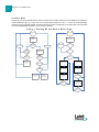
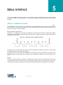
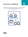
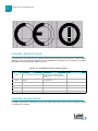
VERSION 1.4
DOCUMENT INFORMATION
Copyright © 2007 Laird Technologies, Inc. All rights reserved.
The information contained in this manual and the accompanying software programs are copyrighted and all rights are
reserved by Laird Technologies, Inc. Laird Technologies, Inc. reserves the right to make periodic modifications of this
product without obligation to notify any person or entity of such revision. Copying, duplicating, selling, or otherwise
distributing any part of this product or accompanying documentation/software without the prior consent of an
authorized representative of Laird Technologies, Inc. is strictly prohibited.
All brands and product names in this publication are registered trademarks or trademarks of their respective holders.
This material is preliminary
Information furnished by Laird Technologies in this specification is believed to be accurate. Devices sold by Laird
Technologies are covered by the warranty and patent indemnification provisions appearing in its Terms of Sale only.
Laird Technologies makes no warranty, express, statutory, and implied or by description, regarding the information
set forth herein. Laird Technologies reserves the right to change specifications at any time and without notice.
Laird Technologies’s products are intended for use in normal commercial and industrial applications. Applications
requiring unusual environmental requirements such as military, medical life-support or life-sustaining equipment are
specifically not recommended without additional testing for such application.
Limited Warranty, Disclaimer, Limitation of Liability
For a period of one (1) year from the date of purchase by the OEM customer, Laird Technologies warrants the OEM
transceiver against defects in materials and workmanship. Laird Technologies will not honor this warranty (and this
warranty will be automatically void) if there has been any (1) tampering, signs of tampering; 2) repair or attempt to
repair by anyone other than an Laird Technologies authorized technician.
This warranty does not cover and Laird Technologies will not be liable for, any damage or failure caused by misuse,
abuse, acts of God, accidents, electrical irregularity, or other causes beyond Laird Technologies’s control, or claim by
other than the original purchaser.
In no event shall Laird Technologies be responsible or liable for any damages arising: From the use of product; From
the loss of use, revenue or profit of the product; or As a result of any event, circumstance, action, or abuse beyond the
control of Laird Technologies, whether such damages be direct, indirect, consequential, special or otherwise and
whether such damages are incurred by the person to whom this warranty extends or third party.
If, after inspection, Laird Technologies determines that there is a defect, Laird Technologies will repair or replace the
OEM transceiver at their discretion. If the product is replaced, it may be a new or refurbished product.
REVISION HISTORY
Revision
Description
Version 1.0
8/29/05 - Initial Release Version
Version 1.1
10/7/05 - Added Declaration of Conformity
Version 1.2
5/29/07 - Updated serial interface section.
response.
Version 1.3
9/18/07 - Internal Release.
Version 1.4
9/5/08- Updated to Laird Technologies branding. Clarified Duty Cycle calculations.
Updated information on client to client communications. Corrected Read
Temperature Command to a max of 0x50. Updated Minimum Baud Rate
Corrected EEPROM write command
Table of Contents
AC4868-250 Transceiver Module 1
AC4868-250 features 1
Overview 1
Specifications 2
Pin Definitions 3
Electrical Specifications 4
Theory of Operation 5
RF Architecture 5
Modes of Operation 5
Duty Cycle Limitations 7
European regulations 7
Radio Operation 7
EEPROM Parameters 26
Dimensions 29
Mechanical Drawings 29
Ordering Information 30
Product Part Number Tree 30
Developer Kit Part Numbers 30
Compliancy Information 31
Agency Identification Numbers 31
Approved Antenna List 31
OEM Equipment Labeling Requirements 31
Country Restrictions 32
Country Notification 32
Declaration of Conformity 33
Appendix I - Sample Power Supply 34
Serial Interface 8
Serial Communications 8
OEM Host Data Rate 9
Serial Interface Baud Rate 9
Interface Timeout / RF Packet Size 10
Flow Control 10
Half Duplex / Full Duplex 11
System Timing & Latency 11
System Throughput 12
Software Interface 13
Networking 13
Range Refresh 13
Auto Config Parameters 13
Max Power 14
Timing Diagrams 15
AC4868-250 Timing Diagrams 15
Hardware Interface 17
Pin Definitions 17
Configuring the AC4868-250 19
AT Commands 20
Command Descriptions 22
Bill of Materials 34
Schematic 35
PCB Layout 35
Appendix II - 5V to 3.3V Levels 37
AC4868-250 T RANSCEIVER M ODULE
1
The compact AC4868-250 868MHz transceiver can replace miles of cable in harsh industrial environments. Using field-proven
technology which needs no additional CE licensing in Europe, OEMs can easily make existing systems wireless with little or no
RF expertise.
AC4868-250 FEATURES
NETWORKING AND SECURITY
•
•
•
•
Drop-in replacement for AC4490 900 MHz & AC4424 2.4 GHz product families
Generic I/O digital lines and integrated DAC/ADC functions
Retries and Acknowledgements
Low latency and high throughput
EASY TO USE
• Software selectable interface baud rates from 1200 bps to 57.6 kbps
• Low cost, low power and small size ideal for high volume, portable and battery powered
applications
• All modules are qualified for Industrial temperatures (-40°C to 80°C)
• Advanced configuration available using AT commands
• Server/Client or peer-to-peer communication
OVERVIEW
The AC4868-250 is a member of Laird Technologies’s ConnexRF OEM transceiver family. The AC4868-250 is
designed for integration into OEM systems operating under European ETSI regulations for the 868 - 870 MHz band.
AC4868-250 transceivers provide an asynchronous TTL/RS-485 level serial interface for OEM Host communications.
Communications include both system and configuration data. The Host supplies system data for transmission to other
Host(s). Configuration data is stored in the on-board EEPROM. All synchronization and RF system data
transmission/reception is performed by the transceiver.
AC4868-250 transceivers can operate in a Point-to-Point, Point-to-Multipoint, or Peer-to-Peer architecture. The
AC4868-250 utilizes a single channel synchronization allowing all radios to communicate with any radio in range.
Optionally any radio can be configured as a Server to provide a synchronization beacon. This beacon is used be the
Client radios to determine In Range status and for Auto Destination addressing.
This document contains information about the hardware and software interface between an Laird Technologies
AC4868-250 transceiver and an OEM Host. Information includes the theory of operation, specifications, interface
definition, configuration information and mechanical drawings. The OEM is responsible for ensuring the final product
meets all appropriate regulatory agency requirements listed herein before selling any product.
Note: Unless mentioned specifically by name, the AC4868-250 modules will be referred to as the “radio” or
“transceiver”. Individual naming is used to differentiate product specific features. The host (PC/Microcontroller/Any
device to which the AC4868-250 module is connected) will be referred to as “OEM Host”.
www.lairdtech.com
2
S PECIFICATIONS
Table 1: AC4868-250 Specifications
General
20 Pin Interface Connector
Molex 87759-0030, mates with Samtec SMM-110-02-S-D
RF Connector
Telegartner J01341C0081, mates with any manufacturer’s MMCX style plug
Antenna
AC4868-250: MMCX Connector
Serial Interface Data Rate
Baud rates from 1200 bps to 57.6 kbps
Power Consumption (typical)
10%TX 50%TX
54mA 138mA
Channels
Single Channel
Security
One byte System ID. 56-bit DES encryption key.
Interface Buffer Size
Input/Output:256 bytes each
100%TX
240mA
100%RX
36mA
Pwr-Down Deep Sleep
TBD
24mA
Transceiver
Frequency Band
Europe 500 mW: 869.4 - 869.65 MHz
RF Data Rate
19.2 kbps or 28.8 kbps dependent on interface baud rate
RF Technology
Single Frequency FSK
Output Power
Conducted (no antenna)
186mW typical
Supply Voltage
Pin 10 (uP power): 3.3 – 5.5V ±50mV ripple; draws ~30-50mA. Must be connected.
Pin 11 (PA power): 3.3 ±3%, ±100mV ripple; draws most current. Must be connected.
Sensitivity
-103dBm typical @ 28.8kbps RF Data Rate
EEPROM write cycles
20000
Hop period
53 ms
Range, Line of Site (based on 2.5dBi gain
antenna)
Up to 15 km (9.3 miles)
EIRP (2.5dBi gain antenna)
250mW typical
Environmental
Temperature (Operating)
-40°C to 80°C
Temperature (Storage)
-50°C to +85°C
Humidity (non-condensing)
10% to 90%
Physical
Dimensions
Transceiver with MMCX Connector: 1.65” x 1.9” x 0.20”
www.lairdtech.com
SPECIFICATIONS
PIN DEFINITIONS
The AC4868-250 has a simple interface that allows OEM Host communications with the transceiver. The table below
shows the connector pin numbers and associated functions. The I/O direction is with respect to the transceiver. All
inputs/outputs are 3.3VDC. All inputs are weakly pulled High and may be left floating during normal operation.
Table 2: AC4868-250 Pin Definitions
Module
Pin
Type
Signal
Name
1
O
GO0
Generic Output pin
2
O
TXD
Transmitted data out of the transceiver
I/O
RS485 A
(True)
I
RXD
I/O
RS485 B
(Invert)
4
I
GI0
5, 16
GND
GND
Signal Ground
N/C
This pin has an internal connection and should be left disconnected.
3
6
Function
Non-inverted RS-485 representation of serial data
Data input to the transceiver
Mirror image of RS-485 A
Generic Input pin
7
O
CTS
Clear to Send – Active Low when the transceiver is ready to accept data for transmission.
8
I
RTS
Request to Send – When enabled in EEPROM, the OEM Host can take this High when it is not ready to
accept data from the transceiver. NOTE: Keeping RTS High for too long can cause data loss.
9
O
GO1
Generic Output pin
10
PWR
VCC1
3.3 – 5.5V, ±50mV ripple. Powers the radio’s uP. Draws ~30-50mA.
11
PWR
VCC2
3.3V, ±50mV ripple. Powers the radio’s power amplifier. Current draw depends on duty cycle and output
power.
12
I
Test
Test Mode – When pulled logic Low and then applying power or resetting, the transceiver’s serial interface
is forced to a 9600, 8-N-1 rate. To exit, the transceiver must be reset or power-cycled with Test Mode logic
High.
N/C
This pin has an internal connection and should be left disconnected.
Generic Input pin
13
14
I
GI1
15
I
UP_RESET
RESET – Controlled by the AC4868-250 for power-on reset if left unconnected. After a stable power-on
reset, a logic High pulse will reset the transceiver.
17
I
CMD/Data
When logic Low, the transceiver interprets OEM Host data as command data. When logic High, the
transceiver interprets OEM Host data as transmit data.
18
I
AD In
19
O
DA_Out
20
O
In_Range
10 bit Analog Data Input
10 bit Analog Data Output
When logic Low, a Client is in range of a Server on same Channel and System ID. Always low on a Server.
www.lairdtech.com
3
4
SPECIFICATIONS
ELECTRICAL SPECIFICATIONS
Table 3: Input Voltage Characteristics
High
Min.
High
Max.
Low
Min.
Low
Max.
Unit
RS485A/B
N/A
12
-7
N/A
V
RXD
2.31
3.3
0
0.99
V
GI0
2.31
3.3
0
0.99
V
RTS
2.31
3.3
0
0.99
V
Test
2.31
3.3
0
0.99
V
GI1
2.31
3.3
0
0.99
V
UP_RESET
0.8
3.3
0
0.6
V
Command/Data
2.31
3.3
0
0.99
V
AD In
N/A
3.3
0
N/A
V
Signal Name
Table 4: Output Voltage Characteristics
Module
Pin
Type
High
Min.
Low
Max.
Unit
GO0
1
O
2.5 @ 8mA
0.4 @ 8mA
V
TXD
2
O
2.5 @ 2mA
0.4 @ 2mA
V
2,3
I/O
3.3 @ 1/8 Unit Load
N/A
V
CTS
7
O
2.5 @ 2mA
0.4 @ 2mA
V
GO1
9
O
2.5 @ 2mA
0.4 @ 2mA
V
DA_Out
19
O
N/A
N/A
V1
In Range
20
O
2.5 @ 2mA
0.4 @ 2mA
V
Signal Name
RS485A/B
1. DA_Out is an unbuffered, high impedance output and must be buffered by the OEM Host when
used.
T HEORY OF O PERATION
3
RF ARCHITECTURE
The AC4868-250 is a single channel radio transceiver. Each unit can be configured as a Server or as a Client.
Servers are responsible for sending out beacons and for allow for radios to be configured very simply in a point-tomultipoint network. Servers are not required for operation, but if they are used, there should only be one Server per
network. All other radios in the network should be configured as Clients. Clients can communicate point-to-point or
in a mesh with or without a Server.
MODES OF OPERATION
The AC4868-250 has three different operating modes; Receive, Transmit, & Command Mode. If the transceiver is not
communicating with another radio, it will be in Receive Mode actively listening for a beacon from the Server. If the
Client determines that the beacon is from a server operating on the same RF Channel and System ID, it will respond
by asserting In_Range Low. A transceiver will enter Transmit or Command mode when the OEM Host sends data over
the serial interface. The state of the Command/Data pin (Pin 17) or the data contents determine which of the two
modes will be entered.
Transmit Mode
All packets sent over the RF are either Addressed or Broadcast packets. Broadcast and Addressed delivery can be
controlled dynamically with the API Control byte and corresponding on-the-fly commands. To prohibit transceivers
from receiving broadcast packets, Unicast only can be enabled.
ADDRESSED PACKETS
When sending an addressed packet, the RF packet is sent only to the receiver specified in destination address. To
increase the odds of successful delivery, Transmit retries are utilized. transparent to the OEM Host; the sending radio
will send the RF packet to the intended receiver. If the receiver receives the packet free of errors, it will return an RF
acknowledge within the same 53 ms hop. If a receive acknowledgement is not received, the radio will use a transmit
retry to resend the packet. The radio will continue sending the packet until either (1) an acknowledgement is received
or (2) all transmit retries have been used. The received packet will only be sent to the OEM Host if and when it is
received free of errors.
BROADCAST PACKETS
When sending a broadcast packet, the RF packet is sent out to every eligible transceiver on the network. To increase
the odds of successful delivery, Broadcast attempts are utilized. Transparent to the OEM Host, the sending radio will
send the RF packet to the intended receiver(s). Unlike transmit retries, all broadcast attempts are used; regardless of
when the RF packet is actually received and without RF acknowledgements. If the packet is received on the first
attempt, the receiver will ignore the remaining broadcast attempts. The received packet will only be sent to the OEM
Host if and when it is received free of errors.
Receive Mode
When a transceiver is not in Transmit or Command mode, it will be in Receive Mode listening for data. While in
Receive Mode, subsequent data of up to 80 bytes can be received every hop (53 ms).
www.lairdtech.com
6
THEORY OF OPERATION
Command Mode
A radio will enter Command Mode when data is received over the serial interface from the OEM Host and either the
Command/Data pin (pin 17) is logic Low or the received data contains the “AT+++” (Enter AT Command Mode)
command. Once in Command Mode, all data received by the radio is interpreted as command data. Command Data
can be either EEPROM Configuration or On-The-Fly commands.
Figure 1: Pending RF and Data in Buffer Flow
Yes
Discard Packet
Receive full
packet and
check CRC
Receive Mode
Receive M ode
Pending RF
Received
Data in Buffer
Broadcast
Packet
Discard Packet
Com mand/Data
Mode
Pin 17 Low
AT+++
Addressed Packet
Yes
Yes
Duplicate
Packet
Matching
Destination
MAC
RF Data
Yes
Send Packet over
RF
Validate CRC
Broadcast Packet
Addressed Packet
Transm it Packet
Transm it Packet
Decrement
Broadcast
Attem pts
Receive ACK
Broadcast
Attem pts = 0
Decrem ent
Transm it Attem pts
Yes
Duplicate
Packet
Send Packet over
RF
Yes
Send RF
Acknowledge
Transm it
Attem pts = 0
4
D UTY C YCLE L IMITATIONS
EUROPEAN REGULATIONS
ETSI requirements as specified in the ETSI EN 300 220-1 define the requirements for the 868-870MHz bands. For a
conducted output of 180mW and radiated outputs up to 500mW, the maximum allowed duty cycle is <10%. This
duty cycle is measured as the amount of TX time on, monitored over one hour and relative to a one hour period. Thus
for the AC4868-250, the maximum “on” time in an hour cannot exceed six minutes.
RADIO OPERATION
The AC4868 will transmit data whenever data is present on the serial UART. Data will be transmitted for Broadcast
packets according to the value of the Broadcast Attempts. For Addressed Packets data will be transmitted until a
successful acknowledgement is received. The OEM is responsible for limiting the Transmitter’s “on” time to less than
the duty cycle regulations.
Transmit Calculations
For a rough estimate the TX Time on is 53ms * the number of retries or attempts. By default this is 212ms. For servers
you need to a 5ms beacon.
The interval time is based on an increment of data equal to or less than the packet size given in the following table.
Table 5: RF Packet Size
RF Baud Rate
Addressed Mode
RF Packet Size
19200
Addressed
0x24
28800
Addressed
0x50
19200
Broadcast
0x40
28880
Broadcast
0x60
So the total TX On Time is 5ms (For Servers) + Data Size/RF Packet Size * Number of Retries/Attempts.
www.lairdtech.com
S ERIAL I NTERFACE
5
In order for the OEM Host and a transceiver to communicate over the serial interface they need to have the same
serial data rate. Refer to the following sections to ensure that the OEM Host data rate matches the serial interface
baud rate.
SERIAL COMMUNICATIONS
The AC4868-250 is a TTL device which can be interfaced to a compatible UART (microcontroller) or level translator to
allow connection to serial devices. UART stands for Universal Asynchronous Receiver Transmitter and its main
function is to transmit or receive serial data.
Asynchronous Operation
Since there is no separate clock in asynchronous operation, the receiver needs a method of synchronizing with the
transmitter. This is achieved by having a fixed baud rate and by using START and STOP bits. A typical asynchronous
mode signal is shown below.
Figure 2: Asynchronous Mode Signal
The UART outputs and inputs logic level signals on the TX and RX pins. The signal is high when no data is being
transmitted and goes low when transmission begins.
The signal stays low for the duration of the START bit and is followed by the data bits; LSB first. The STOP bit follows
the last data bit and is always high. After the STOP bit has completed, the START bit of the next transmission can
occur.
Parity
A parity bit is used to provide error checking for a single bit error. When a single bit is used, parity can be either even
or odd. Even parity means that the number of ones in the data and parity sum to an even number and vice-versa. The
ninth data bit can be used as a parity bit if the data format requires eight data bits and a parity bit as shown below.
www.lairdtech.com
SERIAL INTERFACE
Figure 3: Even Parity Bit
Note: Enabling parity cuts throughput and the interface buffer in half.
OEM HOST DATA RATE
The OEM Host Data Rate is the rate with which the OEM Host and transceiver communicate over the serial interface.
Possible values range from 1200 bps to 57,600 bps. Note: Enabling Parity cuts throughput in half and the Interface
Buffer size in half. The following asynchronous serial data formats are supported:
Table 6: Supported Serial Formats
Data Bits
Parity
Stop Bits
Transceiver Programming Requirements
8
N
1
Parity Disabled
7
N
2
Parity Disabled
7
E, O, M, S
1
Parity Disabled
9
N
1
Parity Enabled
8
N
2
Parity Enabled
8
E, O, M, S
1
Parity Enabled
7
E, O, M, S
2
Parity Enabled
Mark (M) corresponds to 1 & Space (S) corresponds to 0
SERIAL INTERFACE BAUD RATE
This two-byte value determines the baud rate used for communicating over the serial interface to a transceiver. The
Table below lists values for some common baud rates. Baud rates below 1200 and above 57,600 baud are not
www.lairdtech.com
9
10
SERIAL INTERFACE
supported. For a baud rate to be valid, the calculated baud rate must be within ±3% of the OEM Host baud rate. If the
Test pin (Pin 12) is pulled logic Low at reset, the baud rate will be forced to 9,600.
Table 7: Baud Rate / Interface Timeout
Baud Rate
BaudL
(0x42)
BaudH
(0x43)
RF Baud
(not
adjustable)
Minimum Interface
Timeout (0x58)
Stop Bit Delay (0x3F)
57,6001
0xFC
0x00
28,800
0x02
0x03
38,400
0xFA
0x00
19,200
0x02
0x08
28,800
0xF8
0x00
28,800
0x02
0x0E
19,200
0xF4
0x00
19,200
0x03
0x19
14,400
0xF0
0x00
28,800
0x04
0x23
9,600
0xE8
0x00
19,200
0x05
0x39
1. 57,600 is the default baud rate
INTERFACE TIMEOUT / RF PACKET SIZE
Interface Timeout (EEPROM address 0x58), in conjunction with RF Packet Size (EEPROM address 0x5B), determines
when a buffer of data will be sent out over the RF as a complete RF packet, based on whichever condition occurs first.
Interface Timeout – Interface Timeout specifies a maximum byte gap between consecutive bytes. When that byte gap
is exceeded, the bytes in the transmit buffer are sent out over the RF as a complete packet. Interface Timeout is
adjustable in 0.5ms increments and has a tolerance of ±0.5ms. Therefore, the Interface Timeout should be set to a
minimum of 2. The default value for Interface Timeout is 0x04 (2ms) and should be adjusted accordingly when
changing the transceiver baud rate.
RF Packet Size – When the number of bytes in the transceiver transmit buffer equals RF Packet Size, those bytes are
sent out as a complete RF packet. It is much more efficient to send a few large packets rather than several short
packets as every packet the transceiver sends over the RF contains extra header bytes which are not included in the
RF Packet Size. However, if the RF Packet Size is set too large, the transceiver will not be able to send any packets
because the AC4868 requires the entire RF packet to be sent in the same hop period (53 ms). The RF packet size if
programmed in EEPROM automatically when Auto Config is enabled. It is strongly recommended that Auto Config be
left enabled to maximize the efficiency of the transceiver. RF Packet Size must be set to a minimum of 6 in order to
send the Enter AT command.
FLOW CONTROL
Flow control refers to the control of data flow between transceivers. It is the method used to handle data in the
transmit/receive buffer and determines how data flow between the transceivers is started and stopped. Often, one
transceiver is capable of sending data much faster than the other can receive and flow control allows the slower
device to tell the faster device when to pause and resume data transmission.
SERIAL INTERFACE
ENGINEER’S TIP
Can I implement a design using just Txd, Rxd and Gnd (Three-wire Interface)?
Yes. However, it is strongly recommended that your hardware monitor the CTS pin of the radio.
CTS is taken High by the radio when its interface buffer is getting full. Your hardware should
stop sending at this point to avoid a buffer overrun (and subsequent loss of data).
You can perform a successful design without monitoring CTS. However, you need to take into
account the amount of latency the radio adds to the system, any additional latency caused by
Transmit Retries or Broadcast Attempts, how often you send data, non-delivery network
timeouts and interface data rate. Polled type networks, where the Server host requests data
from the Client host and the Client host responds, are good candidates for avoiding the use of
CTS. This is because no one transceiver can monopolize the RF link. Asynchronous type
networks, where any radio can send to another radio at any point in time, are much more
difficult to implement without the use of CTS.
HALF DUPLEX / FULL DUPLEX
When Half Duplex communication is chosen, the AC4868-250 will send a packet out over the RF whenever it can. This
can cause packets sent by multiple transceivers at the same time to collide with each other over the RF. To prevent
this, Full Duplex communication can be chosen. Full Duplex shares the bandwidth intelligently to enable two-way
collision-free communication without any collision. This is done by calculating the amount of time until the next hop to
ensure that it has time to send the packet; if there is enough time, it will send the packet and if not, it will wait until its
next appropriate hop. The Server transmits during the even hops while the Client(s) will transmit during the odd hops.
Although there is technically only one frequency bin, the Server still maintains a bin count for the purpose of handling
Full Duplex mode. While the RF hardware is still technically half duplex, the bandwidth sharing it makes the
transceiver seem full duplex. Enabling Full Duplex can cause overall throughputs to be cut in half.
SYSTEM TIMING & LATENCY
Care should be taken when selecting transceiver architecture, as it can have serious effects on data rates, latency,
and overall system throughput. The importance of these three characteristics will vary from system to system and
www.lairdtech.com
11
12
SERIAL INTERFACE
should be a strong consideration when designing the system.
ENGINEER’S TIP
In High-density applications, what amount of latency should be expected?
It is not easy to predict the exact amount of latency in high-density applications. There are
many variables that affect system latency. The three variables that most affect the latency are
the network load, the distance between transceivers, and whether the transceivers are
operating in a broadcast or addressed mode. There is no fixed answer as to how much latency
will be introduced in the system when considering high-density applications. In these cases we
can just offer qualitative analysis of the latency in high-density applications. As the network
load increases, then the number of collisions that will occur increases. As the number of
collisions increase, then the system latency increases. As the distance between the
transceivers increases, so to does the system latency. Finally, when transceivers operate in
addressed mode they will retry sending a packet up to the number of time specified in the
transmit retry parameter specified in the EEPROM. As the number of retries increases, the
system latency will increase also.
SYSTEM THROUGHPUT
When operating as shown below, an AC4868-250 transceiver is capable of achieving the listed throughput. However,
in the presence of interference or at longer ranges, the transceiver may be unable to meet the specified throughput.
Table 8: Maximum System Throughput
RF Mode
RF Baud
(determined by
Interface Baud)
Half Duplex Throughput
(bps)
Full Duplex Throughput
(bps) each way
Addressed
28,800
15k
7.5k
Addressed
19,200
6.8k
3.4k
Broadcast
28,800
18k
9k
Broadcast
19,200
12k
6k
6
S OFTWARE I NTERFACE
NETWORKING
System ID - System ID (EEPROM address 0x76) is similar to a password character or network number and makes
network eavesdropping more difficult. A transceiver will not establish a Session or communicate with a transceiver
operating on a different System ID or Channel Number.
RF Channel Number -
Table 9: RF Channel Number Settings
RF Channel Number
Range (0x40)
Frequency Details & Regulatory
requirements
0x38
869.4 - 869.65 MHz (Single Frequency. Up to 500 mW
EIRP @ 10% maximum transmit vs. receive duty cycle
Countries
Europe
DES (Data Encryption Standard) - DES (Data Encryption Standard) – Encryption is the process of encoding an
information bit stream to secure the data content. The DES algorithm is a common, simple and well-established
encryption routine. An encryption key of 56 bits is used to encrypt the packet. The receiver must use the exact same
key to decrypt the packet; otherwise garbled data will be produced.
To enable DES, EEPROM Byte 0x45, bit 6 must be set to a value of 1. To disable DES, set bit 6 to a value of 0. The 7
byte (56 bits) Encryption/Decryption Key is located in EEPROM Bytes 0xD0 – 0xD6. It is highly recommended that this
Key be changed from the default.
RANGE REFRESH
Range Refresh - Range Refresh specifies the maximum amount of time a Client reports in range without having heard
a beacon from the Server. Each time the Client hears a beacon, it resets its Range Refresh timer. If the timer reaches
zero, the Client will go out of range, take its In_Range pin High and enter acquisition mode attempting to find the
Server once again. The range refresh is equal to the hop period (53 ms) x Range refresh value.
Note: Range Refresh should not be set to 0x00.
AUTO CONFIG PARAMETERS
The AC4868-250 has several variables that vary by RF mode and architecture. By default, Auto Config is enabled and
bypasses the values stored in EEPROM and uses predetermined values for the given operating mode. Below is a list
www.lairdtech.com
14
SOFTWARE INTERFACE
of the variables controlled by Auto Config and their respective predetermined values. If Auto Config is disabled, these
values must be programmed in the transceiver EEPROM for the corresponding mode of operation.
Table 10: Auto Config Parameters
Parameter
RF Packet Size
EEPROM
Address
0x5B
Default
0x24
RF Baud = 19,200
RF Baud = 28,800
Addressed
Broadcast
Addressed
Broadcast
0x24
0x40
0x50
0x60
MAX POWER
Max Power provides a means for controlling the RF output power of the AC4868. Output power and current
consumption can vary by as much as ±10% per transceiver for a particular Max Power setting. Contact Laird
Technologies for assistance in adjusting Max Power.
ENGINEER’S TIP
The max power is set during Production and may vary slightly from one transceiver to another.
The max power can be set as low as desired but should not be set higher than the original
factory setting. A backup of the original power setting is stored in EEPROM address 0x8E.
T IMING D IAGRAMS
AC4868-250 TIMING DIAGRAMS
Figure 4: Addressed Mode with Timeout
Figure 5: Addressed Mode with Fixed Packet Length
Figure 6: Broadcast Mode with Timeout
www.lairdtech.com
7
16
TIMING DIAGRAMS
Figure 7: Broadcast Mode with Fixed Packet Length
H ARDWARE I NTERFACE
8
Below is a description of all hardware pins used to control the AC4868-250.
PIN DEFINITIONS
Generic I/O
Both GIn pins serve as generic input pins and both GOn pins server as generic output pins. Reading and writing of
these pins can be performed using CC Commands.
TXD & RXD
SERIAL TTL
The AC4868-250 accepts 3.3VDC TTL level asynchronous serial data on the RXD pin and interprets that data as either
Command Data or Transmit Data. Data is sent from the transceiver, at 3.3V levels, to the OEM Host via the TXD pin.
RS-485
When equipped with an onboard RS-485 interface chip, TXD and RXD become the half duplex RS-485 pins. The
transceiver interface will be in Receive Mode except when it has data to send to the OEM Host. TXD is the noninverted representation of the data (RS485A) and RXD is a mirror image of TXD (RS485B). The transceiver will still use
RTS (if enabled).
Hop Frame
Transitions logic Low at the start of a hop and transitions logic High at the completion of a hop. The OEM Host is not
required to monitor Hop Frame. The AC4868 is a single frequency radio that uses fictitious hops, though it generates
a Hop Frame signal every time it transmits a timing beacon.
CTS
The AC4868-250 has an interface buffer size of 256 bytes. If the buffer fills up and more bytes are sent to the
transceiver before the buffer can be emptied, data loss will occur. The transceiver prevents this loss by asserting CTS
High as the buffer fills up and taking CTS Low as the buffer is emptied. CTS On and CTS Off control the operation of
CTS. CTS On specifies the amount of bytes that must be in the buffer for CTS to be disabled (logic High). Even while
CTS is disabled, the OEM Host can still send data to the transceiver, but it should do so carefully.
Note: The CTS On/Off bytes of the EEPROM can be set to 1, in which case CTS will go high as data is sent in and low
when buffer is empty.
GND
Signal Ground. Pins are internally connected.
RTS
With RTS disabled, the transceiver will send any received data to the OEM Host as soon as it is received. However,
some OEM Hosts are not able to accept data from the transceiver all of the time. With RTS enabled, the OEM Host can
prevent the transceiver from sending it data by disabling RTS (logic High). Once RTS is enabled (logic Low), the
transceiver can send packets to the OEM Host as they are received.
www.lairdtech.com
18
HARDWARE INTERFACE
Note: Leaving RTS disabled for too long can cause data loss once the transceiver’s 256 byte receive buffer fills up.
Test / 9600 Baud
When pulled logic Low before applying power or resetting, the transceiver’s serial interface is forced to a 9600, 8-N-1
(8 data bits, No parity, 1 stop bit). To exit, the transceiver must be reset or power-cycled with Test pin logic High. This
pin is used to recover transceivers from unknown baud rates only. It should not be used in normal operation. Instead
the transceiver Interface Baud Rate should be programmed to 9600 baud if that rate is desired for normal operation.
ENGINEER’S TIP
Laird Technologies does not recommend permanently grounding the Forced_9600 pin. This
mode was intended for recovering transceivers from unknown settings and was not intended to
be used in real-time communications.
UP_Reset
UP_Reset provides a direct connection to the reset pin on the AC4868-250 microprocessor and is used to force a soft
reset. For a valid reset, reset must be asserted High for a minimum of 11ms.
Command/Data
When logic High, the transceiver interprets incoming OEM Host data as transmit data to be sent to other transceivers
and their OEM Hosts. When logic Low, the transceiver interprets OEM Host data as command data.
AD In & DA Out
AD In & DA Out can be used as a cost savings to replace Analog-to-Digital and Digital-to-Analog converter hardware.
Reading of this pin can be performed locally using the Read ADC command found in the On-the-Fly Control
Command Reference. DA Out is an unbuffered, high impedance output and MUST be buffered by the OEM Host
when used.
In Range
Reports logic Low when a Client transceiver is in range of a Server radio operating on the same RF Channel and
system ID. If a Client cannot hear a Server for the amount of time defined by Range Refresh, it will drive In_Range High
and enter search mode looking for a Server. When a server is detected, In_Range will be asserted Low. In_Range will
always report Low on Server transceivers.
C ONFIGURING THE AC4868-250
9
The AC4868-250 can be configured using the CC Configuration Commands. The CC Commands can be issued using
either Hardware or Software Configuration. To use Hardware Configuration, pin 17 of a transceiver must be asserted
Low. Software Configuration can be used by entering AT Command Mode before issuing the CC Commands.
Figure 8: AC4868-250 Configuration Flow
Receive Mode
Use AT
Commands
AT+++
(Software
Configuration)
Take Pin 17 Low
(Hardware
Configuration)
No
Send CC
Commands
Send CC
Command
No
No
Send Another
CC Command
www.lairdtech.com
Exit Command
Mode
No
In AT
Command
Mode
No
Send Exit AT
Command Mode
Command
Take Pin 17 High
20
CONFIGURING THE AC4868-250
AT COMMANDS
The AT Command mode implemented in the AC4868-250 creates a virtual version of the Command/Data pin. The
“Enter AT Command Mode” Command asserts this virtual pin Low (to signify Command Mode) and the “Exit AT
Command Mode” Command asserts this virtual pin High (to signify Data). Once this pin has been asserted Low, all
On-the-Fly CC Commands documented in the manual are supported.
On-the-Fly Control Commands
The AC4868-250 transceiver contains static memory that holds many of the parameters that control the transceiver
operation. Using the “CC” command set allows many of these parameters to be changed during system operation.
Because the memory these commands affect is static, when the transceiver is reset, these parameters will revert back
to the settings stored in the EEPROM. While in CC Command mode using pin 17 (Command/Data), the RF interface of
the transceiver is still active. Therefore, it can receive packets from remote transceivers while in CC Command mode
and forward these to the OEM Host.
While in CC Command mode using AT Commands, the RF interface of the transceiver is active, but packets sent from
other transceivers will not be received. The transceiver uses Interface Timeout/RF Packet Size to determine when a
CC Command is complete. Therefore, there should be no delay between each character as it is sent from the OEM
Host to the transceiver or the transceiver will not recognize the command. If the OEM Host has sent a CC Command
to the transceiver and an RF packet is received by the transceiver, the transceiver will send the CC Command
response to the OEM Host before sending the packet. However, if an RF packet is received before the Interface
Timeout expires on a CC Command, the transceiver will send the packet to the OEM Host before sending the CC
Command response.
When an invalid command is sent, the radio scans the command to see if it has a valid command followed by bytes
not associated with the command, in which case the radio discards the invalid bytes and accepts the command. In all
other cases, the radio returns the first byte of the invalid command back to the user and discards the rest.
CONFIGURING THE AC4868-250
Table 11: Command Quick Reference
Command Name
Command (All Bytes in Hex)
Return (All Bytes in Hex)
AT Enter
Command Mode
0x41
0x54
0x2B
0x2B
0x2B
0x0D
0xCC
0x43
0x4F
0x4D
Exit AT Command Mode
0xCC
0x41
0x54
0x4F
0x0D
-
0xCC
0x44
0x41
0x54
Status Request
0xCC
0x00
0x00
-
-
-
0xCC
Firmware
Version
0x00: Server
0x01: Client in range
0x03: Client out of
range
Change Server/Client
0xCC
0x03
0x00: Server
0x03: Client
-
-
0xCC
Firmware
Version
0x00: Server
0x03: Client
Sleep Walk Power Down
0xCC
0x06
-
-
-
-
0xCC
Channel
-
Sleep Walk Wake Up
0xCC
0x07
-
-
-
-
0xCC
Channel
-
Broadcast
Packets
0xCC
0x08
-
0xCC
0x00 or 0x01
-
-
Write Destination Address
0xCC
0x10
Byte 4 of
Dest. MAC
Byte 5
Byte
6
0xCC
Byte 4 of Dest.
MAC
Byte 5
Byte 6
Read Destination Address
0xCC
0x11
-
-
-
0xCC
Byte 4 of Dest.
MAC
Byte 5
Byte 6
Auto Destination
0xCC
0x15
Read Digital Inputs
0xCC
0x20
-
-
-
-
0xCC
bit-0: GI0
bit-1: GI1
Read ADC
0xCC
0x21
0x01: AD In
0x02: Temp
-
-
0xCC
MSB of 10 bit
ADC
Write Digital
Outputs
0xCC
0x23
bit-0: GO0
bit-1: GO1
-
-
0xCC
bit-0: GO0
bit-1: GO1
-
-
Write DAC
0xCC
0x24
-
-
0xCC
Update Period
Duty
Cycle
-
Set Max Power
0xCC
0x25
-
0xCC
Max Power
-
-
Transmit Buffer Empty
0xCC
0x30
-
-
-
-
0xCC
0x00
-
-
Deep Sleep Mode
0xCC
0x86
-
-
-
-
0xCC
Channel
-
-
Read Temperature
0xCC
0xA4
-
-
-
-
0xCC
Temp (C)
-
-
EEPROM Byte Read
0xCC
0xC0
Start Address
0xCC
Starting
Address
Length
Data
EEPROM Byte Write
0xCC
0xC1
Start Address
Length
Data
written
Soft Reset
0xCC
0xFF
-
-
0x00: Broadcast
0x01: Addressed
-
bit-0: Auto Destination
bit-4: Enable Auto Destination
Update
Period
Duty
Cycle
New Max Power
-
-
www.lairdtech.com
0xCC
Length
Length
Data
-
-
bit-0: Auto Destination
bits-1-7: 0
Starting Address
-
-
-
-
-
LSB of 10 bit ADC
21
22
CONFIGURING THE AC4868-250
COMMAND DESCRIPTIONS
E n t e r AT C o m ma n d M o d e
Prior to sending this command, the OEM Host must ensure that the
transceiver’s RF transmit buffer is empty. If the buffer is not empty, the
radio will interpret the command as data and it will be sent over the RF.
This can be accomplished by waiting up to one second between the
last packet and the AT command. RF packet size must be set to
minimum of 6 in order to send this command.
Command: 0x41 0x54 0x2B 0x2B 0x2B 0x0D
Number of Bytes Returned: 4
Response: 0xCC 0x43 0x4F 0x4D
E x it A T C o m m an d M o d e
The OEM Host should send this command to exit AT Command mode
and resume normal operation.
Command: 0xCC 0x41 0x54 0x4F 0x0D
Number of Bytes Returned: 4
Response: 0xCC 0x44 0x41 0x54
S t a t u s R eq u e st
The OEM Host issues this command to request the status of the
transceiver.
Command: 0xCC 0x00 0x00
Number of Bytes Returned: 3
Response: 0xCC Version Data1
Parameter Range: Data1 = 0x00 for Server, 0x01 for Client in
Range, 0x03 for Client out of Range
C ha n g e S er ve r / C li en t
The OEM Host issues this command to change the mode of the
transceiver from Server to Client and vice versa.
Command: 0xCC 0x03 Data1
Number of Bytes Returned: 3
Response: 0xCC Firmware Version Data1
Parameter Range: Data1 = 0x00 for Server, 0x03 for Client
Sl ee p Wal k P o wer - Dow n
After the Host issues this command, the transceiver will de-assert its
In_Range line after entering power down. A Client in power down will
remain in sync with a Server for a minimum of 2 minutes. To maintain
synchronization with the Server, the Client should re-sync at least once
every 2 minutes. This is done by sending the Power Down wake up
command and waiting for the In_Range line to go active. Once this
occurs, the Client is in sync with the server and can be put back into
power-down mode.
Command: 0xCC 0x06
Number of Bytes Returned: 2
Response: 0xCC Channel
This command is valid only for Client transceivers.
S l ee p W al k P o w er - D ow n W a k e U p
The OEM Host issues this command to bring the transceiver out of
Power Down mode.
Command: 0xCC 0x07
Number of Bytes Returned: 2
Response: 0xCC Channel
CONFIGURING THE AC4868-250
B ro ad c a st Pa ck e t s
The OEM Host issues this command to change the transceiver
operation between Addressed Packets and Broadcast Packets. If
Addressed Packets are selected, the transceiver will send all packets to
the transceiver designated by the Destination Address programmed in
the transceiver. If Broadcast Packets are selected, the transceiver will
send its packets to all transceivers on that network. Setting bit-7 of API
Control to 1 can also enable Broadcast Packets.
Command: 0xCC 0x08 Data1
Number of Bytes Returned: 2
Response: 0xCC Data1
Parameter Range: Data1 = 0x00 for Addressed, 0x01 for
Broadcast
W r i t e D e st i n at i o n Ad d r e s s
The OEM Host issues this command to the transceiver to change the
Destination Address.
Command: 0xCC 0x10 MAC3 MAC2 MAC1
Note: Only the three Least Significant Bytes of the MAC Address are
used for packet delivery.
Response: 0xCC MAC3 MAC2 MAC1
Number of Bytes Returned: 4
Parameter Range: 0x00 - 0xFF corresponding to 3 LSB’s of
destination MAC Address
R ea d D e st i n at i o n Ad d r es s
The OEM Host issues this command to the transceiver to read the
destination address.
Command: 0xCC 0x11
Note: Only the three Least Significant Bytes of the MAC Address are
used for packet delivery.
Response: 0xCC MAC3 MAC2 MAC1
Number of Bytes Returned: 4
Parameter Range: 0x00 - 0xFF corresponding to 3 LSB’s of
destination MAC Address
A ut o D es t i na t i o n
The Host issues this command to change the Auto Destination setting.
When issuing this command, the Auto Destination setting will only be
changed if the corresponding enable bit is set (Control1 Parameter,
EEPROM address 0x56, bits-4,5)
Command: 0xCC 0x15 Data1
Number of Bytes Returned: 2
Response: 0xCC Data2
Parameter Range: Data1 = bit-0: Auto Destination, bit-4:
Enable Auto Destination modification; Data2 = bit-0: New
Auto Destination setting, bits 1 - 7:0
R ea d D i g it a l I n p u t s
The OEM Host issues this command to read the state of both digital
input lines.
Command: 0xCC 0x20
Number of Bytes Returned: 2
Response: 0xCC Data1
Parameter Range: Data1 = bit-0: GI0, bit-1: GI1
R ea d A D C
The OEM Host issues this command to read any of the three onboard
10-bit A/D converters. Because the RF is still active in On-the-Fly
Command Mode, the transceiver will not process the command until
there is no activity on the network.
Command: 0xCC 0x21 Data1
Analog Voltage = (10 bits / 0x3FF) * 3.3V
Temperature (oC) = ((Analog Voltage - 0.3) / 0.01) - 30
Parameter Range: Data1 = 0x00: AD In, 0x01: Temperature;
Data2 = MSB of requested 10-bit ADC value; Data3 = LSB of
requested 10-bit ADC value
www.lairdtech.com
Number of Bytes Returned: 3
Response: 0xCC Data2 Data3
23
24
CONFIGURING THE AC4868-250
W r i t e D i g it a l O u t p u t s
The OEM Host issues this command to write both digital output lines to
particular states.
Command: 0xCC 0x23 Data1
Note: This command should only be used when Protocol Status (0xC2)
is not set to 0xE3.
Response: 0xCC Data1
Number of Bytes Returned: 2
Parameter Range: Data1 = bit-0: GO0, bit-1: GO1
W ri t e D A C
The OEM Host issues this command to write DA_Out to a particular
voltage. The transceiver uses a PWM (Pulse Width Modulator) to
generate the analog voltage. The theory behind a PWM is that a binary
pulse is generated with a fixed duty cycle and rate. As such, this pin
toggles between High & Low. This signal is filtered via an on-board R-C
circuit and an analog voltage is generated. Duty cycle specifies the ratio
of time in one cycle that the pulse spends High proportionate to the
amount of time it spends Low. So, with a duty cycle of 50% (0x80), the
pulse is High 50% of the time and Low 50% of the time; therefore the
analog voltage would be half of 3.3V or 1.15V. A broad filter has been
implemented on the transceiver and there is no advantage to using a
slower update period. Generally, a faster update period is preferred.
Command: 0xCC 0x24 Data1 Data2
Number of Bytes Returned: 3
Response: 0xCC Data1 Data2
Parameter Range: Data1 = Update Period; Data2 = Duty
cycle
( 255 × ( Data1 + 1 ) )
T update = ------------------------------------------------6
14.7456
Data2
V out = --------------- × 3.3V
0xFF
Se t M ax Powe r
The OEM Host issues this command to limit the maximum transmit
power emitted by the transceiver. This can be useful to minimize current
consumption and satisfy certain regulatory requirements. The radios
are shipped at maximum allowable power.
Command: 0xCC 0x25 Max Power
Number of Bytes Returned: 2
Response: 0xCC Max Power
T r a n sm i t B u f f e r E m p t y
The OEM Host issues this command to determine when the RF transmit
buffer is empty. The Host will not receive the transceiver response until
that time.
Command: 0xCC 0x30
Number of Bytes Returned: 2
Response: 0xCC 0x00
D ee p S le e p M o d e
The OEM Host issues this command to put the transceiver into Deep
Sleep mode. Once in Deep Sleep mode, the transceiver disables all RF
communications and will not respond to any further commands until
being reset or power-cycled.
Command: 0xCC 0x86
Number of Bytes Returned: 2
Response: 0xCC Channel
This command is valid for both Servers and Clients.
R ea d T e m p er at u r e
The OEM Host issues this command to read the onboard temperature
sensor. The transceiver reports the temperature in oC where 0x00 - 0x50
corresponds to 0 - 80 oC and where 0xD8 - 0x00 corresponds to -40 - 0
o
C.
Command: 0xCC 0xA4
Number of Bytes Returned: 2
Response: 0xCC Temperature
Parameter Range: Temperature = 0xD8 - 0x80
CONFIGURING THE AC4868-250
EE PROM Byte Re ad
Upon receiving this command, a transceiver will respond with the
desired data from the addresses requested by the OEM Host.
Command: 0xCC 0xC0 Data1 Data2
Number of Bytes Returned: 4+
Response: 0xCC Data1 Data2 Data3
Parameter Range: Data1 = EEPROM address; Data2 =
Length (0x00 - 0x80); Data3 = Requested data
EE PROM Byte W ri t e
Upon receiving this command, a transceiver will write the data byte to
the specified address but will not echo it back to the OEM Host until the
EEPROM write cycle is complete (up to 10 ms).
Multiple byte writes of up to 128 bytes are allowed. An EEPROM
boundary exists between addresses 0x7F and 0x80. No single
EEPROM write command shall write to addresses on both sides of that
EEPROM boundary.
Command: 0xCC 0xC1 Data1 Data2
Number of Bytes Returned: 4+
Response: Data1 Data2 Data
Parameter Range: Data1 = EEPROM address; Data2 =
Length (0x00 - 0x80); Data3 = Last byte of Data written
R es et
The OEM Host issues this command to perform a soft reset of the
transceiver. Any transceiver settings modified by CC commands will
revert to the values stored in the EEPROM.
Command: 0xCC 0xFF
Number of Bytes Returned: None
Response: None
www.lairdtech.com
25
10
EEPROM P ARAMETERS
The OEM Host can program various parameters that are stored in EEPROM which become active after a power-on
reset. The table below gives the locations and descriptions of the parameters that can be read/written by the OEM
Host. Factory default values are also shown. Do not write to any EEPROM addresses other than those listed below. Do
not copy one transceiver’s EEPROM to another transceiver as doing so may cause the transceiver to malfunction.
Table 12: EEPROM Parameters
EEPROM
Address
Length
(Bytes)
Product ID
0x00
40
Beacon Period
0x3C
2
0x01
0xFF
-
0x14
Specifies the number of hop periods between Server beacon
transmissions (equal to 53ms * value). Note that each
transceiver should only transmit 10% of the time and
beacons count as transmissions.
Range Refresh
0x3D
1
0x01
0xFF
-
0x18
Specifies the maximum amount of time a transceiver will
report In Range without having heard a Server’s beacon
(equal to hop period * value). Do not set to 0x00.
Stop Bit Delay
0x3F
1
0x00 0xFF
0xFF
For systems employing the RS-485 interface or Parity, the
serial stop bit might come too early. Stop bit delay controls
the width of the last bit before the stop bit occurs.
0xFF = Disable Stop Bit Delay (12 us)
0x00 = (256 * 1.6 us) + 12 us
0x01 - 0xFE = (value * 1.6 us) + 12 us
Channel Number
0x40
1
0x38
0x38
Server/Client Mode
0x41
1
0x01
0x02
-
0x02
0x01 = Server
0x02 = Client
Baud Rate Low
0x42
1
0x00
0xFF
-
0xFC
Low byte of the interface baud rate. Default baud rate is
57,600.
Baud Rate High
0x43
1
0x00
0x00
High byte of interface baud. Always 0x00
Control 0
0x45
1
0x00
0xFF
0x14
Settings are:
bit-7: Laird Technologies Use Only
bit-6: DES Enable
bit-5: Laird Technologies Use Only
bit-4: Laird Technologies Use Only
bit-3: Laird Technologies Use Only
bit-2: Laird Technologies Use Only
bit-1: RF Delivery
Parameter
Range
Default
Description
40 bytes - Product identifier string. Includes revision
information for software and hardware.
-
0 = Addressed packets
1 = Broadcast packets
bit-0: Laird Technologies Use Only
Transmit Retries
0x4C
1
0x01
0xFF
-
0x10
www.lairdtech.com
Maximum number of times a packet is sent out when
Addressed packets are selected.
EEPROM PARAMETERS
Table 12: EEPROM Parameters
EEPROM
Address
Length
(Bytes)
Broadcast Attempts
0x4D
1
0x01
0xFF
-
0x04
Maximum number of times a packet is sent out when
Broadcast packets are selected.
API Control
0x56
1
0x00
0xFF
-
0x43
Settings are:
bit-7: Laird Technologies Use Only
bit-6: Laird Technologies Use Only
bit-5: Unicast Only
Parameter
Range
Default
Description
0 = Disabled
1 = Enabled
bit-4: Auto Destination
0 = Use destination address
1 = Use auto destination
bit-3: Laird Technologies Use Only
bit-2: RTS Enable
0 = Ignore RTS
1 = Transceiver obeys RTS
bit-1: Duplex
0 = Half Duplex
1 = Full Duplex
bit-0: Auto Config
0 = Use EEPROM values
1 = Auto Configure values
Interface Timeout
0x58
1
0x02
0xFF
-
0x04
Specifies a byte gap timeout, used in conjunction with RF
Packet Size to determine when a packet coming over the
interface is complete (0.5 ms per increment).
RF Packet Size
0x5B
1
0x01
0xFF
-
0x24
Used in conjunction with Interface Timeout; specifies the
maximum size of an RF packet. When Auto Config is
enabled, this value is overridden based on the Interface Baud
Rate and RF Delivery mode. Must be set to a minimum of 6 in
order to send the Enter AT command.
CTS On
0x5C
1
0x01
0xFF
-
0xC0
CTS will be deasserted (High) when the transmit buffer
contains at least this many characters.
CTS Off
0x5D
1
0x00
0xFE
-
0xB0
Once CTS has been deasserted, CTS will be reasserted
(Low) when the transmit buffer is contains this many or less
characters.
Max Power
0x63
1
0x00
0x60
-
Set
in
Production
& can vary
Used to increase/decrease the output power.
transceivers are shipped at maximum allowable power.
Parity
0x6F
1
0xE3,
0xFF
0xFF
0xE3 = Enable Parity
0xFF = Disable Parity
Note: Enabling parity cuts throughput and the interface buffer
size in half.
Destination ID
0x70
6
0x00
0xFF
-
0xFF
Specifies destination for RF packets
System ID
0x76
1
0x00
0xFF
-
0x01
Similar to network password. Radios must have the same
system ID to communicate with each other.
RS-485 DE
0x7F
1
0xE3,
0xFF
0xFF
0xE3 = GO0 is active Low DE for control of external RS-485
hardware
0xFF = Disable RS-485 DE
www.lairdtech.com
The
27
28
EEPROM PARAMETERS
Table 12: EEPROM Parameters
EEPROM
Address
Length
(Bytes)
MAC ID
0x80
6
Original Max Power
0x8E
1
Product ID
0x90
15
DES Key
0xD0
7
Parameter
Range
0x00
0xFF
Default
-
Description
Factory programmed unique IEEE MAC address.
Set
in
Production
and can vary
Copy of original max power EEPROM setting. This address
may be referenced but should not be modified.
0x90 - 0x93: Product ID
0x94 - 0x95: Prefix (AC)
0x96 - 0x99: Power (250M)
0x9A - 0x9C: Interface (485, TTL)
0x9D - 0x9E: Setup script (01 is stock)
0x9F: Reserved for future use; always 0xFF
0x00
0xFF
-
56-bit Data Encryption key
11
D IMENSIONS
MECHANICAL DRAWINGS
Interface Connector - 20 pin OEM Interface connector (Molex 87759-0030, mates with Samtec SMM-110-02-S-D
MMCX Jack - Antenna Connector (Johnson Components 135-3711-822)
Figure 9: AC4868-250 (with MMCX connector) Mechanical
2 0 p in h e a d e r , 0 .0 2 0 s q . p o s ts
o n 0 .0 7 9 in c h (2 m m ) c e n te rs
0 .1 5 7
0 .1 8 0
0 .0 6 7
0 .0 6 2
0 .0 0 0
M M C X ja c k
0 .1 2 5 d ia n o n -p la te d h o le s
(2 ) p la c e s
1 .6 5 0
0 .1 0 0 d ia n o n -p la te d h o le
(1 ) p la c e , u n d e r s h ie ld
1 .6 5 0
1 .5 5 0
1 .3 2 0
p in s
1 2
1 .0 1 0
0 .8 2 5
J1
M M C X ja c k 0 .1 4 5 d ia
0 .1 0 0
0 .0 0 0
1.900
1.760
www.lairdtech.com
1.875
0.435
0.000
0.100
0.150
0 .0 0 0
O RDERING I NFORMATION
12
PRODUCT PART NUMBER TREE
DEVELOPER KIT PART NUMBERS
All of the above part numbers can be ordered as a development kit by prefacing the part number with “SDK-”. As an
example, part number AC4868-250M can be ordered as a development kit using the part number: SDK-AC4868250M.
All developer’s kits include (2) transceivers, (2) development boards, (2) 7.5 VDC unregulated power supplies, (2)
serial cables, (2) USB cables, (2) antennas, configuration/testing software and integration engineering support.
www.lairdtech.com
13
C OMPLIANCY I NFORMATION
AGENCY IDENTIFICATION NUMBERS
Agency compliancy is a very important requirement for any product development. Laird Technologies has obtained
modular approval for its products so the OEM only has to meet a few requirements to be eligible to use that approval.
The corresponding agency identification numbers and approved antennas are listed below.
Table 13: Agency Identification Numbers
Part Number
EUR/EN
AC4868-250M
Approved
APPROVED ANTENNA LIST
The following antennas are approved for use with the AC4868-250 as identified. The OEM is free to choose another
vendor’s antenna of like type and equal or lesser gain as a listed antenna and still maintain compliance.
Table 14: AC4868-250 Approved Antennas
Laird
Technologi
es Part
Number
Manufacturer Part
Number
Manufacturer
Type
0600-00020
S467-FL-6-RMM-868S
Nearson
1/2 Wave Dipole
Gain
(dBi)
2
0
0
A
2
0
0
M
1
0
0
0
M
2
-
X
X
OEM EQUIPMENT LABELING REQUIREMENTS
WARNING: The OEM must ensure that the appropriate labeling requirements are met. Following are the requirements
for labeling equipment:
1
If the CE marking is reduced or enlarged, the proportions given in the following graduated drawing must be
respected.
2
The CE marking must have a height of at least 5 mm except where this is not possible on account of the nature of the
apparatus.
3
The CE marking must be affixed to the product or to its data plate. Additionally, it must be affixed to the packaging, if
any, and to the accompanying documents.
4
5
The CE marking must be affixed visibly, legibly, and indelibly.
The exclamation point must be included with the CE mark (as shown below) to alert the user to the fact that there are
restrictions placed on usage in certain countries. It must have the same height as the CE mark.
www.lairdtech.com
32
COMPLIANCY INFORMATION
COUNTRY RESTRICTIONS
The exclamation point included with the CE mark denotes that the equipment has restrictions in certain countries.
Following is a list of countries having restrictions on the AC4868 and a description of those restrictions. The OEM is
responsible for ensuring that these restrictions are met.
Table 15: AC4868 Country Restrictions
RF Channel
Country
Restriction
Reason/Remarks
0x38
All countries (unless otherwise noted)
Maximum ERP of 500 mW and maximum
transmit duty cycle of 10% (amortized over
one hour)
0x38
Bulgaria
Not implemented
0x38
Finland
Audio and voice are not permitted
0x38
Germany
Audio and voice are not permitted
0x38
Italy
Maximum ERP of 25 mW
Military applications
0x38
Slovak Republic
Not implemented
Military
COUNTRY NOTIFICATION
The OEM is responsible for notifying ANY country of the intent to ship product to that country containing the AC4868
four weeks prior to shipping.
COMPLIANCY INFORMATION
DECLARATION OF CONFORMITY
Laird Technologies has issued a Declaration of Conformity for the AC4868-250M transceiver module concerning
emissions, EMC, and safety. The Declaration of Conformity is a document that lists the product name and band of use
and must appear in the OEM user’s manual.
www.lairdtech.com
33
I
A PPENDIX I - S AMPLE P OWER S UPPLY
Below is a simple switching power supply that provides enough current to easily power any Laird Technologies OEM
module. It utilizes low cost, off the shelf components that fit into a small area. This supply has an input voltage range
of +6 volts to +18 volts and will output +3.4 volts at 1.5 amps.
Included is a schematic, bill of materials with manufacture's name and part numbers and a sample PCB layout. It is
important to follow the layout suggestions and use large areas of copper to connect the devices as shown in the
layout. It is also important to hook up the ground traces as shown and use multiple vias to connect input and output
capacitors to the bottom side ground plane.
If the input voltage will be less than 12 volts then C1 and C2 can be replaced with a single 100uF 20 volt capacitor
(same part number as C7). This will reduce board space and lower costs further. If you are powering an AC5124
module, R1 can be changed to a 373 ohm 1% resistor. This will change the output to +5 volts at 1.0 amps.
BILL OF MATERIALS
Table 16: Power Supply Bill of Materials
Qty
Reference
Value
Description
Mfg.
Mfg. part number
1
R1
210
Res, 0603, 210, 1/16W, 1%
KOA
RK73H1JT2100F
1
R2
127
Res, 0603, 127, 1/16W, 1%
KOA
RK73H1JT1270F
2
C1 C2
47uF
Cap, Tant, 7343, 47uF, 35V
AVX
TPSE476M035R0200
3
C3 C4 C5
0.1uF
Cap, Cer, 0603, 0.1uF, Y5V, 25V
Murata
GRM39Y5V104Z025AD
1
C6
3300pF
Cap, Cer, 0603, 3300pF, X7R, 50V
Murata
GRM39X7R332K050AD
1
C7
100uF
Cap, Tant, 7343, 100uF, 20V
Kemet
T491X107K020A5
1
D1
B230/A
Diode, SMB, B230/A, 2A, Schottkey
Diodes, Inc.
B230/A
1
D2
LL4148
Diode, MELF, LL4148, Switch
Diode
Diodes, Inc.
LL4148
1
L1
15uH
Xfmr, 2P, SMT, 15uH, 2A
Coiltronics
UP2.8B150
1
U1
CS51413
IC, CS51413, 8P, SO, Switch Reg
Ctrl.
On-Semicond.
CS51413
www.lairdtech.com
APPENDIX I - SAMPLE POWER SUPPLY
SCHEMATIC
PCB LAYOUT
www.lairdtech.com
35
36
APPENDIX I - SAMPLE POWER SUPPLY
II
A PPENDIX II - 5V TO 3.3V L EVELS
All inputs on the AC4868-250 are weakly pulled high via 10 kohm resistors. The AC4868-250 has 3.3V only inputs.
Some of the most common voltage conversion methods are described below.
Voltage Level Conversion IC’s
This is the easiest and most efficient method. Laird Technologies recommends the TI SN74LVC244A Octal
Buffer/Driver. Inputs can be driven from either 3.3 or 5V systems, allowing the device to be used in a mixed 3.3/5V
system.
1
2
3
4
5
6
7
8
9
10
1OE
VCC
1A0
2OE
2Y3
1Y0
1A1
2A3
2Y2
1Y1
1A2
2A2
2Y1
2Y0
1Y2
1Y3
1A3
GND
2Y0
GND
2A1
2A0
1Y3
2A0
20
19
18
17
16
15
1
14
18
13
16
12
14
11
12
Y0
Y1
Y2
Y3
74LVC244
OE
A0
A1
A2
A3
2
4
6
8
Input A
Input B
Input C
Input D
74LVC244
Passive Resistor Voltage Divider
While a resistor voltage divider can successfully drop the 5V to the required 3.3V, it will draw static current all of the
time. Typically this method is only suitable for one-way 5V to 3.3V conversion. When choosing the resistor values, one
needs to include the radio’s internal 10 kohm resistors on the input signals.
www.lairdtech.com