1
10.4. FPGA Design
72
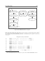
sys_CLK0
lcd_
controller
sdram_A[11:0]
sdram_BA[1:0]
sdram_CAS_n
sdram_RAS_n
sdram_CS_n
sdram_WE_n
sdram_CLK
sdram_CKE
sdram_CLKFB
sdram_DQ[15:0]
sdram_DQM[1:0]
sdram_controller
clock_
synthesizer
lcd_
memory
write_
fifo
trace_
clock
lcd_CS_n
lcd_RST_n
lcd_SID
lcd_SOD
lcd_SCLK
trace_PIPESTAT[2:0]
trace_TRACEPKT[3:0]
trace_TRACESYNC
trace_EXTIN
trace_TRACECLK
read_fifo
usb_D[7:0]
usb_RD_n
usb_WR_n
usb_RXF_n
usb_TXE_n
usb_SIWU
usb_controller
button[3:0]
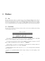
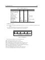
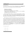
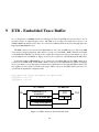
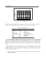
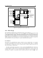
Figure 10.7: OpenOCD+trace trace_capture.vhd
10.4
FPGA Design
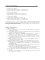
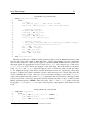
The OpenOCD+trace FPGA design is implemented in the top-level design file trace_capture.vhd.
The top-level design defines the interface to the system (SDRAM, clock, USB, ETM trace port, LCD
module, and user buttons), includes submodules that implement reusable components like the interface
to the SDRAM and USB controllers, and controls the overall behavior. All components except for the
FIFOs used to smooth out SDRAM accesses and the LCD string memory were written from scratch in
VHDL. The FIFOs and LCD string memory were generated using the Xilinx Core Generator. Figure 10.7
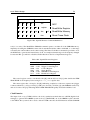
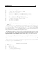
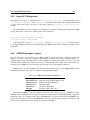
shows the interface to the top level entity trace_capture and the internal components.
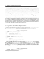
User Interface
The interface to the OpenOCD+trace design is realized via a few commands and a set of registers
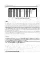
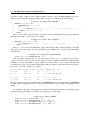
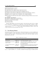
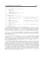
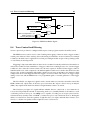
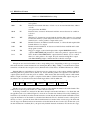
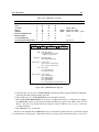
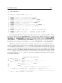
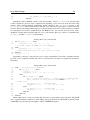
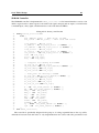
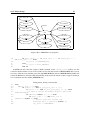
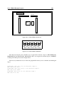
accessible via USB. Figure 10.8 shows the layout of the commands available. Bits 7 to 4 designate
the command, bits 3 to 0 allow up to four bits of data payload per command. Additional data can be sent
and received using more USB transfers.
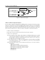
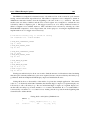
The NOP command 0x0 is implemented to be able to flush the FT245BM FIFO until a defined state
is reached in which no further data bytes are expected and the OpenOCD+trace is ready to accept a new
command. When a register is to be read or written the register’s number has to be placed in bits 2 to 0,
allowing up to 8 registers to be specified, and bit 3 describes the direction of the access (r/w = 0 is a