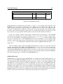
1
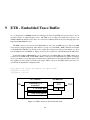
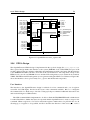
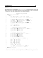
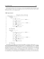
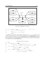
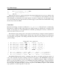
10.4. FPGA Design
82
This addressing scheme allows the memory to be accessed sequentially without incurring a speed
penalty for having to reopen a row on a bank that was just closed, because at the end of any row there
will always follow a row on a different bank.
VHDL Implementation
Listing 10.15: sdram_controller.vhd
73
74
75
76
77
78
79
80
81
82
83
84
85
86
87
88
89
90
91
92
93
94
95
96
97
98
99
100
101
102
103
104
105
architecture Behavioral of sdram_controller is
component read_fifo
port (
clk : IN std_logic ;
din : IN std_logic_VECTOR (15 downto 0);
rd_en : IN std_logic ;
rst : IN std_logic ;
wr_en : IN std_logic ;
dout : OUT std_logic_VECTOR (15 downto 0);
empty : OUT std_logic ;
full : OUT std_logic ;
prog_full : OUT std_logic ;
valid : OUT std_logic ;
wr_ack : OUT std_logic
);
end component;
component write_fifo
port (
din : IN std_logic_VECTOR (15 downto 0);
rd_clk : IN std_logic ;
rd_en : IN std_logic ;
rst : IN std_logic ;
wr_clk : IN std_logic ;
wr_en : IN std_logic ;
dout : OUT std_logic_VECTOR (15 downto 0);
empty : OUT std_logic ;
prog_empty : OUT std_logic ;
full : OUT std_logic ;
valid : OUT std_logic ;
wr_ack : OUT std_logic
);
end component;
The templates for the FIFOs were generated by the Xilinx Core Generator. Because the read_fifo
will only be read and written from the sys_MAINCLK domain it is implemented as a common clock FIFO
using distributed RAM (Distributed SelectRAM). The write_fifo is written from the trace_clk domain
and read from the sys_MAINCLK domain and is therefor implemented using independent clocks and block
RAM (Block SelectRAM). Each of the FIFOs is sixteen bits wide to match the size of the SDRAM
memory the controller is connected to. It would have been possible to implement the write_fifo write
port only eight bits wide, allowing the data from the ETM port to be stored as is, but as the data needs to
be examined anyway to identify trigger and trace-disabled cycles the 16 bit port was chosen because it