1
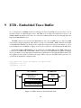
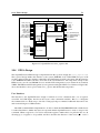
10.4. FPGA Design
577
578
579
580
581
582
583
584
585
586
587
588
589
590
591
89
delay <= 8;
when READ_DATA =>
-- NOP (capture data)
RAS_n <= ’1 ’;
CAS_n <= ’1 ’;
WE_n <= ’1 ’;
rd_fifo_wr_en <= ’1 ’;
if delay = 0 then
rd_fifo_wr_en <= ’0 ’;
counter <= counter - 1;
address <= address + 1;
int_state <= IDLE ;
else
delay <= delay - 1;
end if;
In case of a read request the READ_CMD state is entered, and the READ command is output together
with the bank (from address[7:6]) and column address (address[5:0] and the three least significant bits
zero because of the eight word bursts). The controller then passes through READ_NOP where only one
cycle is spent because the MT48LC8M16A2-7E is fast enough to operate at two cycles CAS latency. If
the memory were slower, requiring three cycles of CAS latency, an additional cycle would have to be
spent in READ_NOP. In READ_DATA the data available on DQ_input is placed into the read FIFO by
asserting the FIFO’s rd_fifo_wr_en signal for eight consecutive cycles. Once the delay reached zero
the controller increments the counter and address, deasserts the write enable signal, and moves back to
IDLE state, ready for the next access.
Listing 10.24: sdram_controller.vhd
592
593
594
595
596
597
598
599
600
601
602
603
604
605
606
607
608
609
610
611
612
613
614
when WRITE_CMD =>
-- WRITE (assert bank and column address)
BA <= address (7 downto 6);
A <= " 000 " & address (5 downto 0) & " 000 ";
RAS_n <= ’1 ’;
CAS_n <= ’0 ’;
WE_n <= ’0 ’;
delay <= 7;
DQ_output_enable <= ’1 ’;
int_state <= WRITE_DATA ;
when WRITE_DATA =>
-- NOP (output data)
RAS_n <= ’1 ’;
CAS_n <= ’1 ’;
WE_n <= ’1 ’;
if delay = 0 then
DQ_output_enable <= ’0 ’;
counter <= counter - 1;
address <= address + 1;
int_state <= IDLE ;
else
if delay = 1 then
wr_fifo_rd_en <= ’0 ’;