1
Using Design-Level Scan to Improve Design
Observability and Controllability for Functional
Verification of FPGAs
Timothy Wheeler, Paul Graham, Brent Nelson, and Brad Hutchings
Department of Electrical and Computer Engineering
Brigham Young University
Provo, UT 84602
{wheelert,grahamp,nelson,hutch}@ee.byu.edu
1
Introduction
With time to market being a chief concern for many hardware designers, shortening the debug and validation time for FPGA-based designs is critical. Software
simulation is a common approach to validating hardware designs since it provides
complete observability and controllability of the design. Unfortunately, software
simulation is extremely slow and can take hours or days to reach some of the
more interesting points in a system’s execution, thus lengthening the design’s
validation time.
Another debug approach is to perform design validation on the existing
FPGA hardware itself. Direct hardware execution is thousands of times faster
than software simulation, and the reconfigurability of FGPAs allows design modifications to be reprogrammed directly onto the FPGA. To be the most effective,
hardware execution should provide the same level of observability and controllability as a software simulator to enable designers to quickly locate and remove
bugs from the design. Observability refers to the ability to access all internal
state of the circuit, similar to the ability of a software debugger to view the values of variables, etc. Controllability is the ability to modify the run-time state of
the circuit, similar to changing the values of program variables in a software debugger. This latter ability is important because it allows the designer to interact
with the design and to change execution flows and infer the root causes of circuit
errors much more quickly. These capabilities should be provided automatically,
without having to generate new configuration bitstreams every time a designer
chooses to view different signals.
Unfortunately, current FPGA systems and software provide very limited observability and controllability for user designs. Two common classes of debug
techniques are ad hoc and structured methods [16]. Examples of ad hoc methods
include some forms of self-test such as signature analysis [13], as well as routing
internal signals to package pads where they can be accessed by a logic analyzer.
The advantages of these approaches are that they have little impact on the area
and speed of the circuit and they allow the circuit to run at full speed during
debug. However, these approaches are painful to use since they require a great
deal of user intervention to implement and current packaging technologies make
it difficult to probe the debug pins. In addition, they provide limited or no observability into the complete state of the user circuit and no controllability at
all.
Some FPGA vendors try to overcome these limitations by providing their own
built-in logic analyzers, such as Xilinx’s ChipScope[18] and Altera’s SignalTap[2,
1]. They allow real-time access to any node on the chip and include the real-time
ability to change the trigger conditions. Unfortunately, although the number of
signals that can be accessed at any given time is greater than for an external
logic analyzer, that number is still limited and the signals must be declared up
front, before the design is run through the place and route tools. Modification to
the signals being viewed or to the size of the data capture buffer often requires
a time-consuming full recompilation of the user design. In addition, these tools
provide no controllability of the user circuit. While these tools may be useful
for speed testing portions of a larger circuit, they are limited in their ability to
provide full functional verification of the user design.
Another common method for debugging FPGA-based designs is configuration readback, which enables users to view the state of their design. Readback
is provided by a number of FPGA vendors, such as Xilinx [5, 9] and Lucent.
An example of the steps required to use readback in obtaining all of the state
information for Xilinx XC4K devices is provided in [8]. Once the readback data
is obtained, [12] describes how it can be used for debugging in a combined simulation/hardware execution environment with JHDL [3, 11].
The advantages of readback are that it theoretically provides complete observability of circuit state and it comes for free from the designer’s viewpoint
when provided as a built-in feature of the FPGA. However, readback has several downsides. First, readback bitstreams can be extremely large and unwieldy,
with only a small percentage of the bitstream being useful for obtaining circuit
state. For example, in a Xilinx Virtex V1000 FPGA, the bitstream contains over
six million bits, only 9% of which represents the device’s flip-flop and memory
state—the rest is configuration data. Second, it is often difficult to obtain the
information telling how the vendor’s software tools mapped the logic to LUTs in
order to locate the state values of interest from the readback bitstream. Third,
in some cases not all FPGA state is accessible via readback. Fourth, performing
a readback sometimes alters the state of the FPGA. The output registers of Virtex BlockRAMs are an example of these last two points. Fifth, for many FPGA
families, no readback support is provided at all, so a different mechanism must
be devised to observe the FPGA’s internal state. Finally, we are unaware of any
readback implementations that provide any controllability.
While the above methods are useful for obtaining observability into the circuit’s state, none of them provide any kind of controllability. Some FPGAs do
provide limited controllability in the form of configuration bitstream modification. Bitstream modification in Xilinx can be done directly using JBits or
indirectly by modifying the .NCD or .XDL files that were created after place
and route, and then running them through bitgen to generate a new configura-
tion bitstream. When loaded into the FPGA, a modified bitstream will initialize
the circuit to the specified state. This allows the user to test corner cases or to
return the circuit to a known state just before a point of failure without the
tedious process of determining a series of inputs that will bring the circuit to
the desired state. The main disadvantages with bitstream modification are that
most FPGA vendors provide no CAD support for doing this, the vendors do not
document the structure of the files that would need to be modified to accomplish
this, and not all FPGA state can be configured in this manner. For example,
in Xilinx Virtex FPGAs, the memories can be configured this way but the flip
flops cannot be.
The methods outlined above, while useful in many instances, are analagous
to using print statements to debug software. For example, the vendor-supplied
embedded logic analyzers allow the designer to specify up front which state “variables”to view, but changes to this usually require a recompilation of the circuit.
In addition to providing only limited circuit observability, none of the methods
provide full controllability, and most of them do not provide any controllability
features at all. What is desired is a mechanism which provides full observability
and controllability into the user design at all times without recompilation. Such
a mechanism would help create a debugging environment similar to a software
debugger, with full observability of the circuit state and the ability to modify
circuit state.
Design-level scan is a structured technique that has been investigated at BYU
as a means of providing such a capability. It is implemented with user circuitry in
a manner similar to the way flip-flop scan chains are employed for VLSI testing
[16]. The rest of this paper explores the use of scan to overcome the limitations
of the debug methods described above to provide complete observability and
controllability for functional verification of FPGA-based designs.
2
Design-Level Scan Implementation
Design-level scan involves wiring up the memory elements, such as flip-flops and
embedded RAMs, in such a way so as to have the state bits contained in these
elements exit the circuit serially through a ScanOut pin whenever the ScanEnable
control signal is asserted. New state data for the FPGA concurrently enters the
circuit serially on the ScanIn pin. When ScanEnable is deasserted, the circuit
returns to normal operation. Design-level scan is different from normal VLSI
scan in that its purpose is to obtain or modify the circuit state in order to
validate the circuit logic, whereas VLSI scan is used to find defects in the silicon
after the logic has already been verified extensively in software.
The benefits of scan are many. First, an FPGA does not require any special
capabilities to implement design-level scan—it can be added to any user design
on any FPGA. Second, the amount of data scanned out of the circuit is much
smaller and easier to manipulate than for readback bitstreams, since scan bitstreams contain only the desired circuit state information. Third, determining
the positions of signal values in the scan bitstream is straightforward since it
is easy to determine the order in which the memory elements are arranged in
the scan chain. Fourth, the state of the entire circuit can be retrieved by scan,
whereas this is not always the case for ad hoc and readback methods. Fifth,
due to the reprogrammable nature of FPGAs, the scan chain can be removed
from the design after verification, thus eliminating the overhead of the scan logic.
Sixth, scan allows the state of the circuit to be set to known values for full circuit
controllability. Lastly, methods like scan can be instrumented systematically and
are not design specific, so the instrumentation processes can be automated. The
biggest downside to scan is the large area and speed penalty it causes, which
will be discussed in greater depth in Section 3. Fortunately, the FPGA can be
configured without scan after the design has been validated, so the overhead is
only temporary.
2.1
Instrumenting Design Primitives
When implementing scan, only memory elements are inserted into the scan
chain1 . This section explains how the primitive memory elements in the Xilinx XC4000 and Virtex libraries are instrumented for scan. Similar techniques
can be applied to other FPGA vendor libraries.
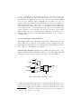
Instrumenting Flip-Flops FPGA flip-flops (FFs) can be inserted into a scan
chain by simply attaching a multiplexor (mux) before the data input of the FF
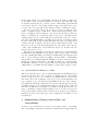
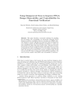
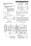
and logic gates in front of the enables and set pins, as shown in Figure 1.
D
0
ScanIn
1
ScanEnable
ScanEnable
Clk En
D
Q
ScanOut
Clk_En
Set
ScanEnable
Set
Clk
Fig. 1. Instrumenting a Flip-Flop for Scan
The ScanIn signal in the figure is the ScanOut from the previous memory in
the scan chain, and the ScanOut signal becomes the ScanIn for the next memory
in the scan chain. Thus, when ScanEnable is asserted, the memories in the circuit
1
Once the state of the memory elements is known, the values for any combinational
portions of the circuit are easy to infer.
form a shift register; when ScanEnable is deasserted the circuit resumes normal
operation. While ScanEnable is asserted, the FF must be enabled and allow its
state bit to be shifted out. The two extra gates in front of the clock enable and
set pins in this example serve this purpose.
The worst-case area overhead for a scannable FF is 300% to add the mux and
two logic gates, but this price is rarely paid. In many instances, clock enables,
sets, and resets in a design are either tied to a constant voltage or shared by
multiple FFs. In the former case, the two gates in Figure 1 are not required; in
the latter case, the gates can be shared by multiple FFs. Also, sometimes the
LUT in front of a FF is empty or has unused inputs, and can thus be used for
either the mux or one of the gates.
Instrumenting ARSW RAMs Inserting asynchronously-read, synchronouslywritten (ARSW) RAMs into scan chains is a bit more complicated than FFs.
Examples of ARSW RAMs include the synchronous LUT RAMs in the Xilinx
XC4000 and Virtex libraries. A RAM has multiple internal values to scan out,
so it is wired up in such a way so as to operate like a FIFO when ScanEnable
is asserted. It outputs its contents one bit per cycle while upstream ScanIn values are concurrently scanned in at one bit per cycle. Similar to the FF shown
in Figure 1, the data input to the RAM is connected to a mux and the write
enable is connected to an OR gate so that scan data is written to the RAM each
clock cycle. The address input to the RAM is also connected to a mux which
selects the output of an address generator whenever ScanEnable is asserted. The
address generator is basically an up-counter that continuously cycles through
all of the RAM addresses. It starts at an address of zero during the first cycle
of scanning out so that the RAM bits are retrieved in a predictable order. The
address generator must also ensure that the RAM contents are scanned back in
at their correct addresses.
The overhead required to instrument an m-bit deep by n-bit wide RAM is
2 × log2 (m) + 1 LUTs for the address generator and log2 (m) + n + 1 LUTs for
the muxes and OR gate to the RAM for a total overhead of 3 × log2 (m) + n + 2
LUTs. If there are multiple RAMs in the circuit, the address generator logic is
shared by all of the RAMs so each additional RAM costs only log2 (m) + n + 1
LUTs to instrument.
Instrumenting Fully Synchronous Embedded RAMs Another type of
RAM to be instrumented for scan is the fully synchronous RAM, such as the
dual-ported Block SelectRAM found in the Xilinx Virtex library. Since both the
reads and writes are synchronous, if the read and write addresses are ever the
same during a given clock cycle, the data at that location will be overwritten
before it is read. Thus, the approach for scan is to inhibit writing to the RAM
during the first cycle of scan to allow the first bit of data to exit the RAM. After
this, writes occur one address behind the reads during scan so as to not overwrite
unread data. Reading and writing to different addresses on the same cycle requires the BlockRAM to be multi-ported; if the BlockRAM is single-ported, it is
simply replaced with its multi-ported counterpart at the time of scan instrumentation. In addition, if the width of the data ports on the BlockRAM is greater
than one bit, serial-to-parallel and parallel-to-serial converters can be placed at
the inputs and outputs to cause the RAM to receive and produce one bit per
cycle in the scan chain. Also, since the contents of a BlockRAM’s output registers cannot be reloaded, shadow registers must be used to capture their contents
during scan. Instrumenting BlockRAMs for scan is very expensive; depending
on the configuration of the BlockRAM, it costs between 80-150 additional LUTs
and 20-80 additional FFs per BlockRAM.
2.2
Instrumenting The Design Hierarchy
Numerous methods can be used to actually instrument a design with scan. A
few methods include making modifications to a placed and routed design, an
EDIF netlist, or a circuit database prior to netlisting in the original CAD tool.
The latter option is the approach of choice within the JHDL design environment
since it is relatively simple to implement and can easily be automated.
In this approach, the user design is placed inside a design “wrapper” that adds
the wires for controlling the scan chain—ScanEnable, ScanIn, and ScanOut —
and connects these and the user wires to I/O pins on the FPGA. In addition,
a ScanMode wire is also added if BlockRAMs are present in the circuit. The
behavior for scanning the data out of a BlockRAM is slightly different than the
behavior for scanning data back in; ScanMode thus indicates whether we are
scanning data in or out of the circuit. The instrumentation tool then traverses
the circuit hierarchy in a depth-first fashion, visiting all design submodules and
inserting all primitive memory elements into the scan chain. This is done by
adding the four scan signals as ports to each hierarchical cell, and adding scan
logic to each flip-flop and embedded RAM, as described previously. Finally,
an address generator is added as needed for controlling the memories. Once the
design is instrumented, an EDIF netlist is generated and run through the FPGA
vendor’s back-end tools.
2.3
FPGA System-Level Issues
The AND gate shown in Figure 1 is to disable the set/reset input to the FF
during scan to prevent the FPGA state from being inadvertently modified while
scan is taking place. This same principle applies to the entire FPGA system so
that reads and writes to external memories are not inadvertently affected by
scan. Writes to external memories can be disabled during scan by tri-stating
the I/O pins of the write enables and connecting them to weak pull-ups (write
enables are active low). In addition, reads and writes to external memories that
have begun, but have not yet completed when scan first begins must be handled.
An easy solution is to buffer the data being read so that it can be used after
scan, and to buffer the data being written to ensure the correct state is still
written to the memories.
3
The Costs of Design-Level Scan
This section discusses the costs of instrumenting user circuits with scan chains.
Some costs include the extra I/O pins used for the ScanIn, ScanOut, ScanEnable,
and ScanMode control signals mentioned in Section 2, as well as storage of the
scan bitstream when operating in scan mode. The main concern to a designer,
however, is the circuit area and speed overhead of scan. Full scan in VLSI has
been reported to require 5% to 30% area overheads [6, 10, 15]. As will be seen
shortly, the area and overhead of full scan in FPGAs is much greater than this.
In addition, we found that adding scan logic on average reduces the speed of the
circuit by 20%.
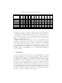
Table 1. Full Scan Costs of User Designs
Design
Original
FF LUT RAM BlockRAM
Count Count
Count
cnt
4
0
0
mult
615
0
0
cordic
768
0
0
Eigenray BF
2216
67
0
Low-power BF 738
1935
30
CDI
4478
40
18
Superquant
4890
3658
0
averages
3.1
LUT
Count
4
270
780
1775
14559
5738
11806
LE
Count
4
630
812
2658
14719
6675
14087
With Full Scan
LUT LUT LE
LE
Count Ratio Count Ratio
9
2.25
9
2.25
871 3.23 871 1.38
1596 2.05 1596 1.97
3413 1.92 3445 1.30
24245 1.67 24391 1.66
12812 2.23 13434 2.01
32192 2.73 32192 2.29
2.30
1.84
Scan Costs for Sample Designs
Consider the scan overheads of several JHDL designs, as shown in Table 1. The
first three designs are basic JHDL library modules and include a 4 bit up-counter,
a 16-bit-by-16-bit, fully-pipelined array multiplier for which only the upper 16
bits of the product are used, and a 16-bit, fully-pipelined rotational CORDIC
unit. The other four circuits are large designs done at BYU and consist of Eigenray BF, which is a heavily pipelined sonar beamformer that does matched field
processing; Low-power BF [14], which consists of a 1024-point FFT unit and
an acoustic beamformer, but is unpipelined due to power constraints; CDI [17],
an ATR unit which performs histogramming and peak finding; and Superquant,
which performs adaptive image quantization to optimally segment images for
target recognition. The beamformers have significant datapaths including multipliers and CORDICs; the other two large designs are control intensive.
Both the original design sizes and their sizes when instrumented with full
scan are shown in Table 1. The LUT count is the number of 4-LUTs contained
in the design, and the logic element (LE) count shows the number of basic logic
blocks, which consist of a single 4-input LUT, carry logic, and a FF. LE counts
are useful for showing the true overhead of scan, for if the FF in a particular LE
is being used, but the corresponding 4-LUT is empty, that 4-LUT can be used
for some of the scan logic without increasing the number of LEs in the design.
As can be seen in the table, both cnt and cordic have roughly the same
number of 4-LUTs as they do FFs in the original design; thus, adding a scan
mux to each FF (as well as adding the other scan logic) effectively doubles the
number of 4-LUTs in the designs. In addition, since most of the LEs in their
original designs used up both the FF and the LUT, little scan logic could be
placed into partially filled LEs, so the LE growth for these two designs is roughly
the same as the LUT growth. Contrast this with mult, where the design area is
dominated mostly by pipeline and skew registers. Thus, while the LUT count
increased by a factor of 3.23 when instrumented for scan, much of the scan logic
could be placed in LEs where only the FF was being used, so the LE count only
increased by a factor of 1.38.
The other four designs in the table have the additional cost of instrumenting
LUT RAMs and BlockRAMs for scan. Eigenray BF can place much of its scan
logic into partially filled LEs, so the LE ratio is significantly lower than the LUT
ratio. Low-power BF has relatively few FFs, so the large number of LUT RAMs
and the high cost of instrumenting BlockRAMs give it most of its 66% increase
in LE area. CDI has many FFs, so the FFs and high cost of instrumenting
BlockRAMs contribute to most of its 101% LE overhead. Lastly, Superquant has
a high number of both FFs and LUT RAMs, so it has a high overhead of 129%.
3.2
Scan Overhead in FPGAs vs. VLSI
This section has shown the costs for implementing full scan in FPGA systems
is much greater than the 5–30% overheads for VLSI mentioned earlier in this
section. So why does scan cost so much more in FPGAs than it does in VLSI?
The answer lies in the granularity of the devices used for implementing scan
logic—transistor logic costs much less than FPGA LUT logic [7]. For example,
[15] claims that a D flip-flop instrumented for scan is only 10% larger in area. In
an FPGA design, however, instrumenting a FF for scan effectively doubles its
size, since the FF and the scan mux are each half of an LE. The size may even
triple or quadruple by using additional LUTs for the clock enable and set/reset
scan logic. In addition, using an entire 4-LUT for the scan mux costs at least 167
transistors [4], whereas the same logic could be implemented in VLSI for about
16 transistors.
4
Supplementing Existing Observability and
Controllability
We have proposed full scan as a method for providing complete observability
and controllability for functional verification of FPGA-based designs. Full scan
is often necessary for providing this capability since many FPGA vendors, such
as Altera and Cypress, have neither built-in observability nor controllability
features. However, many FPGAs, such as those produced by Xilinx, Lucent,
and Atmel, are equipped with limited capability to read or modify the state
of a circuit. Readback and configuration bitstream modification are examples
of such capabilities in Xilinx XC4000 and Virtex FPGAs. Variations of scan
instrumentation can be applied at a fraction of the cost of full scan to supplement
these existing features to provide complete observability and controllability of
the user circuit. This section will show how scan can supplement readback and
bitstream modification on Xilinx XC4000 and Virtex FPGAs to provide complete
observability and controllability of user designs at a lower cost than full scan.
4.1
Supplementing Readback for Observability
The built-in Virtex readback capability essentially provides complete observability. The problem is that doing a readback corrupts the circuit’s BlockRAM
output registers. To fix this, shadow registers can be added to the circuit to
capture the output registers of the BlockRAMs and preserve their state for use
immediately after readback. This eliminates the need for full scan for observability. Thus, full observability via readback can be achieved for very low cost
as will be shown later.
4.2
Supplementing Bitstream Modification for Controllability
Xilinx FPGAs provide the ability to externally modify the state of their LUT
RAMs and BlockRAMs through configuration bitstream modification; however,
the state of the FFs cannot be modified externally. Thus, one option to provide
full controllability of Xilinx FPGAs is to use bitstream modification techniques
to control the state of the LUT RAMs and BlockRAMs, and to use scan to
control just the FFs. The area overhead for this method consists of the cost of
instrumenting the FFs for scan and a minimal amount of extra logic required to
disable all other memories to preserve their state during scan.
4.3
Best-Case Results
Table 2 shows the results of supplementing Xilinx’s built-in observability and
controllability features with variations of full scan. The left section provides
the overhead required if the designer is only interested in obtaining complete
observability of the circuit. The overhead is in the form of shadow registers as
discussed in Section 4.1 which fix the readback limitations in Virtex BlockRAMs.
Since only Low-power BF and CDI use BlockRAMs, they are the only designs
affected by the extra logic.
The middle section shows the overhead required if the designer only desires
full controllability of the circuit. In this case, only the FFs are instrumented for
scan, while the the state of the embedded RAMs are controlled via bitstream
Table 2. Best-Case Results for Xilinx Designs
Design
Full Observability
LUT LUT LE
LE
Count Ratio Count Ratio
cnt
4
1.00
4
1.00
mult
270 1.00 630 1.00
cordic
780 1.00 812 1.00
Eigenray BF
1775 1.00 2658 1.00
Low-power BF 14809 1.01 15231 1.03
CDI
6065 1.06 7368 1.10
Superquant
11806 1.00 14087 1.00
averages
1.01
1.02
Full Controllability
LUT LUT LE
LE
Count Ratio Count Ratio
9
2.25
9
2.25
871 3.23 871 1.38
1596 2.05 1596 1.97
3306 1.86 3427 1.29
16035 1.10 16035 1.09
10945 1.91 10945 1.64
20342 1.72 20342 1.44
2.02
1.58
LUT
Count
9
871
1596
3306
16362
11371
20342
Both
LUT LE
Ratio Count
2.25
9
3.23 871
2.05 1596
1.86 3427
1.12 16584
1.98 11679
1.72 20342
2.03
modification, as described in Section 4.2. This approach is particularly useful
for designs that either have relatively few FFs or that were paying a huge price
to instrument their RAMs with full scan, such as Low-power BF, CDI and Superquant. However, the state of the other designs in the table consist mostly of
FFs, so for them this approach results in about the same circuitry as instrumenting the design with full scan.
Finally, the right section of Table 2 shows the cost of supplementing existing Xilinx debug features with a combination of the readback shadow registers
and scanning only the FFs to provide complete observability and controllability
of user designs. It shows a 60% LE overhead, as opposed to the 84% overhead
associated with full scan. Although this is certainly an improvement, it shows
that since FPGA vendors currently do not provide full observability and controllability features on their FPGAs, the cost of obtaining such capabilities for
debug is very high.
5
Conclusions
None of the currently available methods for debugging FPGA-based circuits
provide the full ability to view and modify the circuit state. This work has shown
how full scan can be used to overcome their limitations to provide complete
observability and controllability of user designs. It comes at a high price, though,
with full scan costing an additional 84% in area overhead on average. When
scan techniques are used to supplement readback and configuration bitstream
modification for Xilinx XC4000 and Virtex designs, the overhead is reduced to
60%. Although the costs in either case are still high, they may be justified if the
designer can take advantage of fast hardware execution rather than be forced to
use software simulation to validate the design; thus, reducing its overall “timeto-market”. In addition, design-level scan costs are temporary since the scan
logic can be removed for the final production design.
LE
Ratio
2.25
1.38
1.97
1.29
1.13
1.75
1.44
1.60
References
1. Altera Corporation, San Jose, CA. SignalTap User’s Guide, 1999.10 (revision 2)
edition, November 1999.
2. Altera Corporation, San Jose, CA. SignalTap Embedded Logic Analyzer Megafunction Data Sheet, ver. 1.01 edition, January 2000.
3. P. Bellows and B. L. Hutchings. JHDL - an HDL for reconfigurable systems. In
J. M. Arnold and K. L. Pocek, editors, Proceedings of IEEE Workshop on FPGAs
for Custom Computing Machines, pages 175–184, Napa, CA, Apr. 1998.
4. V. Betz, J. Rose, and A. Marquardt. Architecture and CAD for Deep-Submicron
FPGAs, chapter Appendix B, page 216. The Kluwer International Series in Engineering and Computer Science. Kluwer Academic Publishers, Boston, 1999.
5. C. Carmichael. VIRTEX configuration and readback. Application Note XAPP
138, Xilinx, San Jose, CA, 1999.
6. A. L. Crouch. Design for Test for Digital IC’s and Embedded Core Systems, chapter 3, page 97. Prentice Hall PTR, Upper Saddle River, NJ, 1999.
7. A. DeHon. Reconfigurable Architectures for General-Purpose Computing. PhD
thesis, Massachusetts Institute of Technology, September 1996.
8. P. Graham, B. Hutchings, and B. Nelson. Improving the fpga design process
through determining and applying logical-to-physical design mappings. Technical
Report CCL-2000-GHN-1, Brigham Young University, Provo, UT, April 2000.
9. W. Hölfich. Using the XC4000 readback capability. Application Note XAPP 015,
Xilinx, XC4000, San Jose, CA, 1994.
10. S. L. Hurst. VLSI Testing: Digital and Mixed Analogue/Digital Techniques, chapter 5, page 218. Number 9 in IEE Circuits, Devices and Systems Series. Institution
of Electrical Engineers, London, 1998.
11. B. Hutchings, P. Bellows, J. Hawkins, S. Hemmert, B. Nelson, and M. Rytting.
A cad suite for high-performance fpga design. In K. L. Pocek and J. M. Arnold,
editors, Proceedings of the IEEE Workshop on FPGAs for Custom Computing
Machines, page n/a, Napa, CA, April 1999. IEEE Computer Society, IEEE.
12. B. L. Hutchings and B. E. Nelson. Unifying simulation and execution in a design
environment for fpga systems. IEEE Transactions on VLSI Systems, to appear.
13. A. D. F. M. Abramovici, M. A. Breuer. Digital Systems Testing and Testable
Design, chapter 10, page 421. Computer Science Press, New York, NY, 1990.
14. S. Scalera, M. Falco, and B. Nelson. A reconfigurable computing architecture
for microsensors. In K. L. Pocek and J. M. Arnold, editors, Proceedings of
the IEEE Symposium on Field-Programmable Custom Computing Machines, page
TBA, Napa, April 2000. IEEE Computer Society, IEEE Computer Society Press.
15. M. J. S. Smith. Application Specific Integrated Circuits, chapter 14, page 764.
Addison-Wesley, Reading, Mass., 1997.
16. T. W. Williams and K. P. Parker. Design for testability - a survey. IEEE Transactions on Computers, C-31(1):2–15, January 1982.
17. M. Wirthlin, S. Morrison, P. Graham, and B. Bray. Improving the performance
and efficiency of an adaptive amplification operation using configurable hardware.
In K. L. Pocek and J. M. Arnold, editors, Proceedings of the IEEE Symposium on
Field-Programmable Custom Computing Machines, page TBA, Napa, April 2000.
IEEE Computer Society, IEEE Computer Society Press.
18. Xilinx, San Jose, CA. ChipScope Software and ILA Cores User Manual, v. 1.1
edition, June 2000.