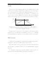
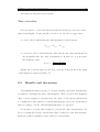
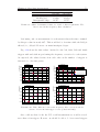
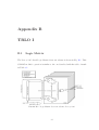
1
Universidade de Lisboa
Faculdade de Ciências
Departamento de Fı́sica
A new Trigger Logic system
for the LAND/R3B setup
Ana Isabel Martinho Henriques
Mestrado em Engenharia Fı́sica
2010
Universidade de Lisboa
Faculdade de Ciências
Departamento de Fı́sica
A new Trigger Logic system
for the LAND/R3B setup
Ana Isabel Martinho Henriques
Mestrado em Engenharia Fı́sica
Tese orientada pelo Doutor
Daniel Galaviz Redondo
2010
“I rarely end up where I was intending to go, but often I end up somewhere
that I needed to be”
Douglas Adams
Abstract
The trigger logic system of an experimental apparatus is responsible for the
data acquisition of that system, i.e., this system decides when data is to be collected. the LAND/ R3 B collaboration trigger logic system was updated for the
2010 campaign.
In this update the several parts of the trigger system in the different modules
were included in one FPGA. This new module so-called VULOM is now responsible
for the hole trigger logic and for setting the overall dead time. The FPGA use
now implies a 10 ns jitter in the trigger logic signals.
This thesis contains the description of the trigger logic system, the old and also
the one included in the VULOM. In order to completely understand a experimental
setup and the role of the trigger logics, it is necessary to go from the detectors
through the conversion of electrical signals to the storage of data.
This insight of the electronic setup allowed to start a dead time measurement
project. This measurement project main goal is to keep under surveillance the
local dead time of the several subsystems. To perform this, it is necessary to keep
in mind how the system works and how to synchronize CPU clocks. A plan was
outlined and a simulation program was developed to check for its feasibility. Our
results suggest that the time required to perform the measurement can be reduced
by 30% if the CPU clocks are only corrected with the clocks offset, disregarding the
frequency offset. However some simulation improvements are required to further
conclusions.
Contents
Abstract
ii
List of Figures
vi
List of Tables
viii
Abbreviations
ix
1 Introduction
1
2 GSI and the LAND group
2.1 GSI . . . . . . . . . . . . . . . . . . . . . . . . . . . . . . . . . . . .
2.2 The LAND experimental setup . . . . . . . . . . . . . . . . . . . .
4
4
5
3 Reading out detector signals
3.1 Detection of particles with scintillators
3.2 Electronic signals . . . . . . . . . . . .
3.3 Electronic modules . . . . . . . . . . .
3.3.1 ADCs and QDCs . . . . . . . .
3.3.2 Discriminators . . . . . . . . . .
3.3.3 TDCs . . . . . . . . . . . . . .
3.3.4 Delays and stretchers . . . . . .
.
.
.
.
.
.
.
.
.
.
.
.
.
.
.
.
.
.
.
.
.
.
.
.
.
.
.
.
.
.
.
.
.
.
.
.
.
.
.
.
.
.
.
.
.
.
.
.
.
.
.
.
.
.
.
.
.
.
.
.
.
.
.
.
.
.
.
.
.
.
.
.
.
.
.
.
.
.
.
.
.
.
.
.
.
.
.
.
.
.
.
.
.
.
.
.
.
.
.
.
.
.
.
.
.
.
.
.
.
.
.
.
9
9
11
13
13
14
15
16
4 DAQ
17
4.1 Triggerless and triggered systems . . . . . . . . . . . . . . . . . . . 17
4.2 LAND DAQ . . . . . . . . . . . . . . . . . . . . . . . . . . . . . . . 18
5 Previous trigger logic system
5.1 LAND Trigger system . . . . . .
5.1.1 Trigger logic input . . . .
5.1.2 Logic matrix unit . . . . .
5.1.3 Trigger box . . . . . . . .
5.1.4 Priority encoder . . . . . .
5.2 The MBS and the TRIVA module
iii
.
.
.
.
.
.
.
.
.
.
.
.
.
.
.
.
.
.
.
.
.
.
.
.
.
.
.
.
.
.
.
.
.
.
.
.
.
.
.
.
.
.
.
.
.
.
.
.
.
.
.
.
.
.
.
.
.
.
.
.
.
.
.
.
.
.
.
.
.
.
.
.
.
.
.
.
.
.
.
.
.
.
.
.
.
.
.
.
.
.
.
.
.
.
.
.
.
.
.
.
.
.
.
.
.
.
.
.
.
.
.
.
.
.
21
21
21
25
26
27
28
Contents
iv
6 TRLO II - VULOM
6.1 Code structure . . . . . . . . . . . . . . . . .
6.2 Trigger Logic II - fast path and state machine
6.2.1 Fast path . . . . . . . . . . . . . . . .
6.2.1.1 Logic Matrix Unit . . . . . .
6.2.1.2 Fast path timing . . . . . . .
6.2.2 State machine . . . . . . . . . . . . . .
6.3 Tracer . . . . . . . . . . . . . . . . . . . . . .
6.4 The module front panel . . . . . . . . . . . . .
6.4.1 Display . . . . . . . . . . . . . . . . .
6.4.2 LEDs . . . . . . . . . . . . . . . . . .
7 VULOM control and settings
7.1 Multiplexers . . . . . . . . . .
7.2 Setups of logic functions . . .
7.3 Scalers . . . . . . . . . . . . .
7.4 Fast path settings and outputs
7.5 State machine settings . . . .
7.6 MBS settings . . . . . . . . .
8 Dead time measurement
8.1 Clock synchronization
8.2 Measurements . . . . .
8.3 Working plan . . . . .
8.4 Simulations . . . . . .
8.5 Results and discussion
.
.
.
.
.
.
.
.
.
.
.
.
.
.
.
.
.
.
.
.
.
.
.
.
.
.
.
.
.
.
.
.
.
.
.
.
.
.
.
.
.
.
.
.
.
.
.
.
.
.
.
.
.
.
.
.
.
.
.
.
.
.
.
.
.
.
.
.
.
.
.
.
.
.
.
.
.
.
.
.
.
.
.
.
.
.
.
.
.
.
.
.
.
.
.
.
.
.
.
.
.
.
.
.
.
.
.
.
.
.
.
.
.
.
.
.
.
.
.
.
.
.
.
.
.
.
.
.
.
.
.
.
.
.
.
.
.
.
.
.
.
.
.
.
.
.
.
.
.
.
.
.
.
.
.
.
.
.
.
.
.
.
.
.
.
.
.
.
.
.
.
.
.
.
.
.
.
.
.
.
.
.
.
.
.
.
.
.
.
.
.
.
.
.
.
.
.
.
.
.
.
.
.
.
.
.
.
.
.
.
.
.
.
.
.
.
.
.
.
.
.
.
.
.
.
.
.
.
.
.
.
.
.
.
.
.
.
.
.
.
.
.
.
.
.
.
.
.
.
.
.
.
.
.
.
.
.
.
.
.
.
.
.
.
.
.
.
.
.
.
.
.
.
.
.
.
.
.
.
.
.
.
.
.
.
.
.
.
.
.
.
.
.
.
.
.
.
.
.
.
.
.
.
.
.
.
.
.
.
.
.
.
.
.
.
.
.
.
.
.
.
.
.
.
.
.
.
.
.
.
.
.
.
.
.
.
.
.
.
.
.
.
.
.
.
.
.
.
.
.
.
.
.
.
.
.
.
.
.
.
33
34
36
36
38
41
41
47
50
50
52
.
.
.
.
.
.
54
54
56
57
58
58
59
.
.
.
.
.
62
63
67
69
70
74
9 Conclusions and future work
78
A LAND setup
80
A.1 Experimental apparatus . . . . . . . . . . . . . . . . . . . . . . . . 80
B TRLO I
B.1 Logic Matrix
83
. . . . . . . . . . . . . . . . . . . . . . . . . . . . . . 83
C TRLO II
C.1 Fast path and State machine inputs
C.2 VULOM settings . . . . . . . . . .
C.2.1 Multiplexer indices . . . . .
C.2.2 Logic functions settings . . .
C.2.3 Scaler modes . . . . . . . .
C.2.4 Trigger settings . . . . . . .
C.3 Map of ’Setups’ . . . . . . . . . . .
C.4 Map of ’Outputs’ . . . . . . . . . .
and outputs
. . . . . . .
. . . . . . .
. . . . . . .
. . . . . . .
. . . . . . .
. . . . . . .
. . . . . . .
.
.
.
.
.
.
.
.
.
.
.
.
.
.
.
.
.
.
.
.
.
.
.
.
.
.
.
.
.
.
.
.
.
.
.
.
.
.
.
.
.
.
.
.
.
.
.
.
.
.
.
.
.
.
.
.
.
.
.
.
.
.
.
.
.
.
.
.
.
.
.
.
.
.
.
.
.
.
.
.
.
.
.
.
.
.
.
.
84
84
84
85
87
87
88
89
91
Contents
v
D Crystal Ball cabling
93
D.1 New Crystal Ball electronics . . . . . . . . . . . . . . . . . . . . . . 93
Bibliography
100
Acknowledgements
102
List of Figures
2.1
2.2
GSI and FAIR accelerator complex . . . . . . . . . . . . . . . . . .
The LAND setup scheme for the 2010 campaign . . . . . . . . . . .
3.1
3.2
3.3
3.4
Scintillator detector with PMT . . . . . . . . . . .
Electronic signal . . . . . . . . . . . . . . . . . . .
Leading edge discriminator - walk and jitter effects
Constant fraction discriminator operation . . . . . .
4.1
LAND DAQ scheme . . . . . . . . . . . . . . . . . . . . . . . . . . 19
5.1
5.2
5.3
5.4
5.5
Trigger logic input - SUM operation . . .
Trigger logic input for the POS detector
Trigger Logic structure . . . . . . . . . .
Readout system scheme . . . . . . . . .
Readout through the MBS . . . . . . . .
.
.
.
.
.
.
.
.
.
.
.
.
.
.
.
.
.
.
.
.
.
.
.
.
.
.
.
.
.
.
22
22
24
28
29
6.1
6.2
6.3
6.4
6.5
6.6
6.7
6.8
6.9
6.10
6.11
6.12
6.13
TRLO II code main structure . . . . . . . . . . . . . . . .
From trigger inputs to master start generation (fast path)
Anti-metastable function . . . . . . . . . . . . . . . . . . .
Delay implementation . . . . . . . . . . . . . . . . . . . .
Logic matrix electronic scheme for one channel . . . . . . .
Fast path time measurement setup scheme . . . . . . . . .
State machine scheme . . . . . . . . . . . . . . . . . . . .
State machine input scheme . . . . . . . . . . . . . . . . .
Fast path and state machine interdependencies . . . . . . .
Fast path and state machine time diagram . . . . . . . . .
Trigger inputs alignment - the tracer state machine . . . .
Module front panel . . . . . . . . . . . . . . . . . . . . . .
VULOM module display . . . . . . . . . . . . . . . . . . .
.
.
.
.
.
.
.
.
.
.
.
.
.
.
.
.
.
.
.
.
.
.
.
.
.
.
.
.
.
.
.
.
.
.
.
.
.
.
.
.
.
.
.
.
.
.
.
.
.
.
.
.
.
.
.
.
.
.
.
.
.
.
.
.
.
35
37
37
38
39
41
42
43
45
47
48
50
51
7.1
Direct vs Logic mode, time measurements scheme . . . . . . . . . . 55
8.1
8.2
8.3
8.4
8.5
CPU slow and fast clocks . . . . . . . . . . . . . . .
CPU fast clock linear compensation scheme . . . .
Clock synchronization using Cristian’s algorithm . .
Clock synchronization with Network Time Protocol
Dead time limiting steps in the readout process . .
vi
.
.
.
.
.
.
.
.
.
.
.
.
.
.
.
.
.
.
.
.
.
.
.
.
.
.
.
.
.
.
.
.
.
.
.
.
.
.
.
.
.
.
.
.
.
.
.
.
.
.
.
.
.
.
.
.
.
.
.
.
.
.
.
.
.
.
.
.
.
.
.
.
.
.
.
.
.
.
.
.
.
.
.
.
.
.
.
.
.
.
.
.
.
.
.
.
.
.
.
.
.
.
.
.
.
.
.
.
.
.
.
.
.
.
.
.
.
.
.
.
.
.
.
.
.
.
5
6
12
12
14
15
64
64
65
66
68
List of Figures
vii
8.6
8.7
NTP application in the DT measurement . . . . . . . . . . . . . . .
Display of the measured Dead Time. The display was coded using
python matplotlib libraries. . . . . . . . . . . . . . . . . . . . . . .
8.8 Processor clock simulation concept . . . . . . . . . . . . . . . . . .
8.9 Offset measure simulation concept . . . . . . . . . . . . . . . . . . .
8.10 Last trigger drift measure . . . . . . . . . . . . . . . . . . . . . . .
8.11 Time difference between with and without correction for 100 triggers
71
72
73
75
77
A.1
A.2
A.3
A.4
A.5
80
81
81
82
82
Beam entry in cave C . . .
Crystal ball and target . .
Target wheel . . . . . . . .
ALADIN, GFIs and PDCs
TFW and DTF detectors .
.
.
.
.
.
.
.
.
.
.
.
.
.
.
.
.
.
.
.
.
.
.
.
.
.
.
.
.
.
.
.
.
.
.
.
.
.
.
.
.
.
.
.
.
.
.
.
.
.
.
.
.
.
.
.
.
.
.
.
.
.
.
.
.
.
.
.
.
.
.
.
.
.
.
.
.
.
.
.
.
.
.
.
.
.
.
.
.
.
.
.
.
.
.
.
.
.
.
.
.
.
.
.
.
.
.
.
.
.
.
.
.
.
.
.
69
B.1 Logic Matrix electronic scheme, Lecroy 2365 . . . . . . . . . . . . . 83
C.1 Fast path inputs and outputs . . . . . . . . . . . . . . . . . . . . . 84
C.2 State machine inputs and outputs . . . . . . . . . . . . . . . . . . . 85
D.1 Previous and current Crystal Ball electronic scheme . . . . . . . . . 94
D.2 Crystal Ball scale model . . . . . . . . . . . . . . . . . . . . . . . . 95
List of Tables
2.1
Detectors and measured quantities . . . . . . . . . . . . . . . . . .
5.1
5.2
5.3
5.4
5.5
LMU trigger inputs . . . . . . . . . . . . . . . . .
Correspondence between the detector triggers and
List of RIO processors used in the 2010 campaign
Logic matrix file for On Spill triggers . . . . . . .
Logic matrix file for Off Spill triggers . . . . . . .
6.1
6.2
6.3
6.4
Logic matrix table of truth . . . . . . . . . . . . . . . . . . . . . .
State machine states (Trigger states) . . . . . . . . . . . . . . . .
Inputs/options that lead to the different states of the state machine
(Reason). (FP - fast path) . . . . . . . . . . . . . . . . . . . . . .
Signals in the VULOM’s front panel LEDs . . . . . . . . . . . . .
7.1
7.2
Fast path registers and outputs. . . . . . . . . . . . . . . . . . . . . 58
State machine signals, registers and outputs options. . . . . . . . . 59
8.1
8.2
Simulations settings . . . . . . . . . . . . . . . . . . . . . . . . . . . 71
Offset determination times . . . . . . . . . . . . . . . . . . . . . . . 75
viii
. . . . . . . . . .
hardware triggers
. . . . . . . . . .
. . . . . . . . . .
. . . . . . . . . .
8
24
27
30
31
32
. 39
. 52
. 52
. 53
Abbreviations
ADC
Amplitude to Digital Converter
ALADIN A Large DIpole magNet
ASIC
Application Specific Integrated Circuit
BoS
Begining of Spill
CFD
Constant Fraction Discriminator
CLB
Configurable Logic Block
CPU
Central Processing Unit
CVT
Conversion Time
DAQ
Data AcQuisition System
DT
Dead Time
EoS
End of Spill
ESR
Experimental Storage Ring
FAIR
Facility for Antiproton and Ion Research
FPGA
Field-Programmable Gate Array
FRS
FRagment Separator
GSI
GSI Helmholtzzentrum für Schwerionenforschung GmbH
GFI
Grosse FIber detector
HDL
Hardware Descriptive Language
LAND
Large Area Neutron Detector
LDT
Local Dead Time
LE
Leading Edge
LMU
Logic Matrix Unit
LUT
Lookup Table
NTP
Network Time Protocol
ix
Abbreviations
x
MBS
Multi Branch System
MUX
MUltipleXer
PE
Priority Encoder
POS
POsition Sensitive detector
ppm
parts per million
PSP
Position Sensitive Pin diode
PMT
Photo Multiplier Tube
QDC
Charge to Digital Converter
R
Reason
R3B
Reactions with Relativistic Radioactive Beams
ROLU
Rechts, Oben, Links, Unten
SIS
SchwerIonenSynchrotron
SSD
Silicon Strip Detectors
TAC
Time-to-Amplitude Converter
TB
Trigger Box
TS
Trigger State
TCAL
Time CALibrator
TDC
Time to Digital Converter
TFW
Time-of-Flight Wall
TOF
Time-of-Flight
tpat
trigger pattern
TRIVA
Trigger synchronization module
TRLO I
Previously running TRigger LOgic
TRLO II
New TRigger LOgic
UNILAC
UNIversal Linear ACcelerator
VHDL
Very high speed integrated circuit HDL
VULOM
VME Universal LOgic Module
Chapter 1
Introduction
The LAND (Large Area Neutron Detector) collaboration is experimentally
studying the properties of exotic and unstable nuclei. This group carries out
experiments in inverse kinematics with both stable and unstable isotope beams.
The LAND ( group studies for example halo nuclei, multiphonon giant resonances,
collective flow of nuclear matter and multi fragmentation [1, 2].
Moving towards FAIR (Facility for Antiprotons and Ion Research) and in particular to the R3 B collaboration (Reactions with Relativistic Radioactive Beams),
the LAND group at GSI (GSI Helmholtzzentrum für Schwerionenforschung GmbH)
is upgrading the electronic components of its experimental apparatus.
The Nuclear Physics Center of the University of Lisbon recently joined the
efforts of the R3 B collaboration to study halo nuclei. Aiming for the determination
of the ground state spectroscopic factors of the halo nuclei
11
Be and 15 C in inverse
kinematics using quasi-free scattering reactions. The main goal of this study is to
get a firm ground concerning the theory of these nuclei, following the Fadaeev/AGS
formalism.
That recent collaboration started with the improvement of the trigger logic.
After getting acquainted with the previously running trigger logic (TRLO I), the
main effort was placed in the development of a new trigger logic (TRLO II).
1
Chapter 1. Introduction
2
The new trigger logic is implemented in a FPGA (Field-programmable Gate
Array) on a module denominated VULOM (VME Universal LOgic Module). The
VULOM hardware was developed by Jan Hoffmann at the GSI electronics department. The VULOM FPGA code was first developed by Jochen Fruehauf and later
modified and generalized to the LAND setup by Håkan Johansson.
This thesis is an introduction to the trigger logic system in the LAND setup.
Also included is a short introduction to detector generated electronic signals in
order to understand the overall process involved in a experimental setup like the
LAND detection apparatus. This first approach with the LAND setup allowed
also to start a new project to measure the dead time of the individual subsystems
of the setup which is also included in the thesis.
***
The thesis is divided in 8 main chapters. Chapter 2 contains the description
of the GSI facility and in particular the LAND/R3 B collaboration experimental
apparatus for the 2010 campaign. In chapter 3 is introduced one detection system,
a scintillator detector. Follows the modules necessary to transform the detectors
electrical signals into time and energy information.
In chapter 4 introduces the triggered LAND data acquisition system, making
emphasis in the trigger logic system and the process involved from getting a master
start to the storage of data. The next chapter is a description of the previously
running trigger logic system. Here we go from the trigger logic inputs to the
readout of the systems through the MBS.
The subject of chapter 6 is the new trigger logic system which is described
in detail in its main structures. The fast path, from the trigger inputs to the
generation of one master start, and also the state machine, responsible for the
final trigger identification and dead time management. The following chapter
holds all the VULOM settings in particular the ones used in MBS.
Chapter 1. Introduction
3
In chapter 8, the dead time measurement project is introduced. It is made
an introduction to the concepts necessary to this project in particular CPU clock
synchronization. After looking at the main issues of the project a plan is also
outlined. In order to check this plan simulations were proposed. Its results are
also shown in this chapter.
Chapter 2
GSI and the LAND group
2.1
GSI
GSI is a scientific research facility in Darmstadt, Germany. This heavy ion
accelerator facility strives to ”understand the structure and behavior of the world
that surrounds us”. The research fields cover nuclear and atomic physics, plasma,
materials research, biophysics and cancer therapy. A schematic view of the facility
is presented in Fig. 2.1, in blue the present GSI and in red the future FAIR complex
[1].
At the GSI accelerator, it is possible to prepare ion beams of all elements, up
to and including uranium and accelerate them to a significant fraction of the speed
of light.
A primary beam is generated by ion sources at the left most side of the complex.
The beam is injected in the linear accelerator (UNILAC), with its 120 m, the ions
are accelerated up to 20 percent of the speed of light. The beam is then accelerated
in the GSI synchrotron, the SIS18 (SchwerIonen Synchrotron). Here, the ions are
accelerated up to 90 percent of the speed of light, which means 1 AGeV for
238
U.
From the SIS18 the beam can be directed to the FRS (FRagment Separator). Here, relativistic beams of exotic nuclei can be produced and separated
4
Chapter 2. GSI and the LAND group
5
Figure 2.1: GSI and FAIR accelerator complex [1]. The future FAIR facility
is in red while the present GSI complex is in blue.
into isotopically-pure components, by in-flight fragmentation. The primary beam
interacts with a target producing a broad distribution of nuclei, the resulting secondary beam is then selected according to the magnetic field settings applied in
the FRS dipoles. The secondary beam is delivered to several experimental setups
(Cave A, B and C) and also the ESR (Experimental Storage Ring) [1, 3].
The ESR stores and accumulates ions up to the highest possible currents. Here
it is possible to obtain very small angular divergences and velocity distributions
by applying special techniques like electron- or stochastic-cooling [4].
2.2
The LAND experimental setup
The LAND setup is presently housed in Cave C. For the August to October
2010 campaign, experiments s393, s306 and s389, the setup will be as follows.
Fig. 2.2 is a scheme of the experimental setup.
Chapter 2. GSI and the LAND group
6
Accelerated in the SIS18 a beam will be selected to enter the cave by in-flight
fragmentation in the FRS. The beam entering the cave will be characterized by
several detectors (time, position), allowing to resolve the different nuclei in the
beam. The first detector is the PSP (Position Sensitive Pin diode) detector, a
silicon detector, used to determine the energy loss of an ion passing through. This
will allow particle identification and beam tracking via the Bethe-Bloch formula.
The next detector is the ROLU (Rechts, Oben, Links, Unten). This detector
consists of four scintillator paddles displaced, leaving a rectangle in the middle
to define the accepted beam spot size. This detector acts as a veto system, i.e.
in case it ”sees” something, the event generated by this particle/ion will not be
recorded. Also at the entrance of cave C is the so-called POS detector, a quadratic
plastic scintillator. The time information of this detector together with other
time measurements from other scintillators upstream in the FRS, can be used to
determine the time of flight of the incoming ions.
CRYSTAL
BALL
ROLU
PSP/PIXEL
VETO
WALL
ALADIN
Si
LAND
PSP/PIXEL
POS
target
30
15
GFI
TFW
TOF FRAGMENTS
PROTON
DRIFT CHAMBERS
DTF
TOF PROTONS
Figure 2.2: The LAND setup scheme for the 2010 campaign. This setup aims
to measure energies, positions and time of flight. The beam entering from the
right will face some detectors (PSP, ROLU and POS) until it reaches the target
at the center of Crystal Ball. The fragments from the reaction will be deflected
by the magnet and its features are measured in its deflection line.
The incoming beam will then collide with the target placed inside the Crystal
Ball, a 4π 162 NaI crystals gamma detector. This detector is also prepared to
measure the energy deposit of scattered protons in its forward hemisphere. Around
Chapter 2. GSI and the LAND group
7
the target one can find several Silicon Strip Detectors (SSD). These are used to
track charged particles.
After the collision with the target the resulting fragments with beam direction
go through the dipole magnet ALADIN (A Large DIpole magNet) and are deflected
according to their magnetic rigidity into different branches.
Straight ahead one can find LAND (LArge Neutron Detector), a 2 x 2 x 1 m3
neutron detector composed of sandwiched iron and scintillator layers. This detector performs Time of Flight (TOF) measurements of neutrons. Between the
magnet and LAND is the Veto wall. This is a scintillator detector used to detect
charged particles which were produced during the particles trajectories after the
ALADIN. At an angle of 15◦ with respect to the incoming beam axis, the heavy
fragments from the reaction pass through the GFI (Grosse FIber Detector) detectors, scintillating fiber detectors used for position determination. The heavy
fragments are finally characterized by a scintillator TOF Wall, TFW.
Similarly the protons coming out of ALADIN are detected by two drift chambers and a scintillator TOF wall, DTF. These detectors are located at 30◦ with
respect to the incoming beam axis [2].
The measured quantities in the detectors of the LAND setup are summarized
in Table 2.1.
Chapter 2. GSI and the LAND group
Detector
S2 and S8
PSP
PIXEL
ROLU
POS
Crystal ball
Silicon
LAND
GFI
TFW
NTF
Drift cambers
DTF
Measurement
Tof measurement
Beam tracking/ ∆E measurement
PSP calibration
Beam spot size accepted
Tof of incoming beam
E measurement for γ and protons
Tracking (∆E and position)
Tof of neutrons
Tracking
Tof, charge and position measurement of fragments
Tof (with TAQUILA)
Trajectories of protons
Tof, charge and measurement of protons
Table 2.1: Detectors and measured quantities in the LAND/R3 B setup.
8
Chapter 3
Reading out detector signals
A detector is a device that converts the passing of a particle into a measurable
quantity via interactions with the detector material. Depending on the particle
and detector the interaction involved is different. To describe this conversion
process, let us look at the example of a scintillator detector.
3.1
Detection of particles with scintillators
Scintillating detectors are amongst the most used in nuclear physics. It is
usually a crystal or a plastic scintillator coupled to a PMT (photomultiplier tube).
A scintillator is a material which exhibits luminescence, i.e., emits a flash of
light, after being struck by ionizing radiation. This material emits low-energy
photons, usually in the visible range. Helped by total internal reflection and light
guides, the photons are transported to the PMTs.
The absorption and emission of radiation can occur by two processes. If it
occurs within the first 100 µs the process is named fluorescence. If it finds a metastable excited state and it takes more time, it is called phosphorescence. In this
type of material it can take hours to emit the radiation.
9
Chapter 3. Reading out detector signals
10
For a single scintillation event, the time evolution of the number of emitted
photons, N, can often be described by the linear superposition of one or two
exponential decays, where two decay constants can be identified. Scintillators can
be characterized by these two time components: τf and τs , the fast and the slow
decay constants:
t
N = A exp −
τf
t
+ B exp −
τs
The relative amplitude A and B of the two components depends on the scintillating material. Usually the the fast component dominates, [5]. Both of these
components can also be a function of the energy loss dE/dx.
There are several types of scintillator materials, each one of them with their
own properties: organic crystals, organic liquids, plastics, inorganic crystals, gases
and glasses [5].
Properties
When coupled to a PMT the emitted radiation can be converted to an electrical
signal which can be used to identify the properties of the incident particle.
• Energy linearity
Scintillators reveal a good sensitivity to the ionizing radiation energy. Above
a certain energy threshold, the light output of most scintillators is proportional to the energy deposited. Avoiding non-linear behavior of a PMT,
the amplitude of the electrical signal will be proportional to the deposited
energy.
• Fast Time Response
The time response of a scintillator detector is short when compared to other
detectors. This feature turns scintillators into excellent tools for timing
measurements.
Chapter 3. Reading out detector signals
11
Scintillator detectors also reveal a good time in recovering from the previous
signal, this means that the intrinsic detector dead time is short.
• Particle discrimination
Certain scintillators allow particle identification by analyzing the shape of
the emitted light pulses. Different pulses result from different fluorescence
mechanisms caused by different particles.
Photomultiplier Tube
A PMT is not only a device that converts photons into electrons but also an
amplifier, [5]. At the entrance of the PMT is a photocathode which converts
photons into electrons by the photoelectric effect. After the cathode there are
several dynodes and at the end an anode. This structure exhibits a potential
ladder from the cathode to the anode, so the electrons emitted at the cathode are
accelerated from dynode to dynode, until they reach the anode. In each dynode,
the number of electrons is multiplied. For each electron that arrives several can be
emitted and accelerated to the next dynode. Finally, in the anode the electrons
are collected into an electric pulse.
Fig. 3.1 is a representation of a scintillator crystal coupled to a photomultiplier
tube.
3.2
Electronic signals
An electronic signal, logic or analog, has some features that can be visualized
with an oscilloscope, allowing its characterization. Operations performed to a
signal may depend on the signal properties. The most simple property is the
signal’s amplitude, the signal’s highest voltage value. In other words, its peak.
When this value is surpassed for a small time interval, an overshoot is present. An
Chapter 3. Reading out detector signals
−HV
R1
Charged
particle
R2
12
R3
R4
Dynodes
Scintilator
Anode
Photocathode
R5
R6
R7
R8
Figure 3.1: Scintillator detector with PMT. The photons resulting from the
de-excitation of the scintillator material are guided to the PMT. The PMT converts the photons into electrons and multiplies their number in the consecutive
dynodes, leading to s signal amplification. At the output of the photomultiplier
an electrical signal results from the collection of the electron charge.
overshoot is most likely to occur when filters are used to minimize the rise time of
a signal. The amplitude and the risetime of a signal is represented in Fig. 3.2.
T1
T2
time
10%
Amplitude
voltage
90%
Rise time
Figure 3.2: Electronic signal, its amplitude and risetime.
The rise time is the time required for a signal to swing from 10% to 90% of its
peak value. One can also refer to a signals fall time, for the time necessary to go
from 90 % 10% of its amplitude, from its full value.
Another signal feature is its beginning and ending, the first is referred as the
leading edge while the second the trailing edge.
A signal can be catalogued as unipolar (one polarity, positive or negative) or
bipolar (positive and negative polarity).
In electronics the major division that one can make with signals is to classify
them as analog or digital. While analog refers to a continuous signal with varying
Chapter 3. Reading out detector signals
13
amplitude, a digital signal is a discrete signal in time, where the voltage variations
are discrete and the values take jumps when increasing or decreasing. Although
a digital signal is linked to a present or not present behaviour, in fact when seen
through a scope it will show a rise time different from zero, as an analog signal.
As previously mentioned, the analog pulse coming out of the PMT carried
a charge related to the energy loss, ∆E, of the particle detected. Added to it,
the relative time of that pulse matters. The pulse must then be electronically
processed in order to obtain those two pieces of information.
3.3
Electronic modules
The signals from the detectors must be treated and transformed in order to be
useful for further analysis. They carry all the information related to the particle
detected. In a experimental setup where time and energy are the main observables,
the frontend electronics is composed by some specific modules such as Charge/Amplitude Digital Converters, discriminators and Time to Digital Converters [5].
3.3.1
ADCs and QDCs
An ADC (Amplitude to Digital Converter) and a QDC (Charge to Digital
Converter) generate a digital word ”proportional” to the analog input. In nuclear
physics, these devices are used in energy measurements.
While ADCs take into account the signal’s peak, the QDCs take its charge.
In the first case, the digitized value corresponds to the height of the signal. As
for the charge sensitive QDC, the output is related to the integrated input signal.
In both cases, a gate is necessary. In the ADC, it is necessary to limit the time
Chapter 3. Reading out detector signals
14
window to search for a peak, as for the QDC one needs to specify the integration
time.
3.3.2
Discriminators
Discriminators are electronic modules that produce a logic pulse with a precise
timing relative to an input signal. Discriminators are also used for ignoring noise
pulses.
At the input of a discriminator one can find analog signals with different amplitudes, arriving randomly in time. As for the output, it is a logic pulse that
only depends on the arrival time, having a defined amplitude and width. There
are two main categories of discriminators, leading edge (LE) and constant fraction
discriminators (CFD).
The LE discriminator is the simplest of the two discriminators mentioned
above. Given an input pulse, as soon as its amplitude is above a defined signal height, a logic signal is produced.
The LE trigger reveals a handicap when the inputs are two signals coincident
in time but with different amplitudes. The pulse with lower amplitude will require
more time to reach the threshold. As a result the output pulse will be shifted in
time, this is called walk. Also some jitter may appear as the signal is not noise
free and may present fluctuations, this will introduce some fluctuations in reaching
the threshold. Fig. 3.3 illustrates these effects.
a)
b)
shift
shift
C
Threshold
A
B
Figure 3.3: Leading edge discriminator: a) The walk effect revealed by higher
amplitude signal B and a smaller amplitude A; b) Signal with jitter. In both
cases the variations in the signals introduce a shift in the output time
Chapter 3. Reading out detector signals
15
The CFD makes use of a more precise method when compared with the LE.
It is, to first approximation, not amplitude dependent. The CFD uses a predetermined constant fraction, f, of the input signal amplitude to determine the
time relation between the input and output pulse.
The CFD also requires that the pulse goes through a threshold. Then the input
signal is splitted. One is inverted and reduced by the factor f, the other is delayed.
The delay should be chosen carefully, by taking into account the expected rise time.
If the delay is too short the output will be produced sooner than it should, i.e.,
there will be walk. The two signals are then be added, giving a bipolar signal.
The logical output is produced at zero crossing, as a result of the adding function.
This is represented in Fig. 3.4.
Figure 3.4: CFD: The input pulse (dashed curve) is delayed resulting on the
dotted line. The input is also inverted and downscaled (dot-dashed curve). The
bipolar signal (solid curve) results from adding the two previous curves. The
CFD output will come at the zero crossing of the solid curve, t.
The CFD is a good option compared to the LE discriminator when considering
signals with almost the same shape, otherwise the walk will also arise. However
a LE should also be taken into account as it is simpler and faster, i.e., does not
require delay.
3.3.3
TDCs
A TDC (Time to Digital Converter) is a device that measures a time interval
between two events, a START and a STOP, and gives it in a digital form.
Chapter 3. Reading out detector signals
16
A common version of a TDC can be represented as a TAC (Time to Amplitude Converter) followed by a ADC (Amplitude to Digital Converter). The TAC
produces a signal whose amplitude is proportional to the time interval between th
e START and the STOP signals. This usually works by charging a capacitor, the
capacitor starts charging when the START signal comes, until the STOP signal.
The charge collected, over a resistor, is sent to the output. This output is then
proportional to the time elapsed between signals. Via a ADC this output is then
converted to a digital format.
Another conversion consists in counting a clock between a start and stop signal.
3.3.4
Delays and stretchers
Sometimes it is necessary to delay signals. Especially early signals or signals
generated closer to a checkpoint, where they must arrive at the same time. This
would be the case when one wants to make coincidences between signals, in order
to compare their presence they must arrive at that point at the same time.
The delays are done with delay gates or just by adding cable length in their
path. The later case is the most reliable as the signal charge is kept, even though
features like height are attenuated.
Also related to coincidences, it is necessary to compare signals with the same
features, specially time length. In order to do this a stretcher is necessary. The
function of this module is to extend the input signal. This takes into consideration
the different detector’s response time and signal delay before reaching the trigger
logic system.
Chapter 4
DAQ
The Data AcQuisition (DAQ) system is responsible for the automatic collection
of data. It is the software coordinator of all the processes from the collection of
the converted data to its storage. Depending on the physic studied, not only the
experimental setup is constructed but it is also necessary to adjust the acquisition
system according to the kinds of events wanted.
4.1
Triggerless and triggered systems
When ions are entering the experimental cave, some of them will interact with
the target leading to the reaction(s) of interest. However most of the ions will
not interact or interact with inactive detector material, the air, gas, etc. Cosmic
particles could also be detected. All those induces a lot of information that is
not required. Furthermore, the conversion time, the data re-collection and storage
need some time.
In order to record mostly events of interest, an overall electronic and DAQ
trigger is built.
17
Chapter 4. DAQ
18
A triggered system will only gather data if certain requirements are fulfilled.
This introduces the concepts of SUM, OR and coincidence/anticoincidence between signals. For the trigger to be fired one may ask for a SUM of certain signals
or an OR. Also, one can require that certain detector signals arrive at the trigger
system in a certain time interval (coincidence) or even the absence of one signal
compared to other (anticoincidence). These signals requirements guarantee that
the signal is not just a sporadic one from one detector. On the one hand, a triggered system will not need such a large memory capacity. On the other hand, it
needs for its implementation a large electronic structure, that increases with the
complexity of the experimental setup.
However with the development and for certain reactions, having a common
trigger for all the detectors induce an artificially high dead time. New setups are
then developed without a hardwire event trigger, the so-called triggerless systems.
In case of such a system, the signals at the output of the converters are just
sampled through. The data is timestamped and an event is recovered in software
by an event builder with the help of the timestamps. This method tries to overcome
part of the dead time limitation, although the conversion time will still contribute
to the dead time. Despite of all electronics that cease to be necessary to generate
the trigger, a triggerless system will require a large amount of memory and more
processing power in order to perform the software triggering.
The current LAND data acquisition system is trigger based. Electrical signals
will only be collected, processed and stored if certain conditions are fulfilled.
4.2
LAND DAQ
The LAND DAQ electronic modules are placed inside in and outside cave C.
Looking throughout one channel, Fig.4.1, helps one to get the idea of the process
involved in the LAND experimental setup.
Chapter 4. DAQ
19
Analog signal
Trigger Logic
Master Trigger
Logic pulse
TL input
CFD
Detector
DAQ
Delays
TDC
Event Builder
Splitter
Delays
Network
QDC
Storage
Figure 4.1: LAND DAQ scheme. In the LAND setup to get the time and
energy information each signal from a detector is splitted. One line for time
measurement with a TDC and the other with a QDC for energy. The signals
gathered after the CFD (Sum) is the input of the trigger logic. When this
system verifies certain conditions, the DAQ initiates the data collection and its
storage processes, by generating some gates. The gates are delivered to the
TDCs and QDCs to get the data at its output. The data obtain there is then
delivered to the Event Builder, where the data is associated in events. These
are stored in a mass storage.
The detector signals are splitted in two branches. One for the time and the
other for the energy measurements. So in one branch one will find a TDC and in
other, for the energy, a QDC.
Once in the TDC line, the signals go through a CFD and only after head to
the TDC. The CFD is only appropriated for this branch as it is only necessary to
account for the signal’s time for the time measurements and its logical value for
the trigger decision.
In the parallel QDC line, the signals are delayed and then enter the QDCs.
The delay is such that it takes into account not only the time of the CFD in the
TDC branch but also the trigger time, time enough that all the signals from the
detectors throughout the cave arrive and to make a trigger decision.
From the CFD is obtained the trigger logic input signals that is delivered to
the trigger logic, this means that even if a detector got several hits in several places
for the trigger it will count as one hit in that detector.
During the conversion time, the trigger logic acts like a traffic light, with a
pass or no pass option for the data gathering and conversion.
Chapter 4. DAQ
20
If the trigger requests are fulfilled the trigger logic ”triggers” the acquisition
by generating the so-called master start. The master start will then lead to the
generation of gates for ADCs and QDCs, after the conversion, the data from the
TDCs and QDCs is collected and sent to the Event Builder. In the Event Builder
the data is associated and labelled as an event. After that the data, now as
standard GSI lmd file, is sent through the network to a computer for data storage
[6, 7].
The processes between the trigger logic decision and the data collection consume time, during which other hits can occur. However, the modules are already
performing their task. Therefore, the data corresponding to thoses hits cannot be
recorded: this is the dead time. It is mainly due to the time needed to convert the
data and it is estimated for TRLO I to be around 400 µs, 300 µs required for the
slowest converters to convert and 100 µs for their readout.
Chapter 5
Previous trigger logic system
5.1
LAND Trigger system
In an experimental physics setup in which the data acquisition is triggered, the
DAQ will only start upon a decision of the trigger logic. This will only produce
an output signal to be delivered to the DAQ depending on the pattern of signals
received and if the system is able to accept them, i.e., not in dead time. In the
following, the features of the trigger logic in the LAND setup are explained.
5.1.1
Trigger logic input
A large detector system, like the Crystal Ball, contains several individual detectors, each of them delivering a different output. A particle interacting with the
detector system may induce a signal in some of the individual units. However, as
far as the trigger logic is concerned, the detector will produce one logic pulse.
Several operations can be applied to the analog signals from the detectors. The
most simple one is an OR of all the CFD signals from one detector system. This
means that in case that one or more of the individual detectors ”sees” something,
there will be a logic pulse sent to the trigger system.
21
Chapter 5. Previous trigger logic system
22
Another possible operation is to set a minimum number of fired detectors by
analog adding of the detector pulses and compare the result to a threshold value.
Just as this threshold is reached a pulse is sent to the trigger system. This can be
seen in Fig. 5.1.
Detector
Discriminator
Detector
Discriminator
Detector
Discriminator
SUM
LE
Trigger System
Figure 5.1: Trigger logic input - SUM operation. The signals delivered to the
trigger logic in certain cases correspond to the sum of several detector outputs
and only when a certain value is reached a signal representing these inputs is
delivered to the trigger logic.
Let us now consider one of the detectors present at the LAND setup. The POS
detector has in its structure one scintillator sheet and four photomultiplier tubes,
one at each side, see Fig. 5.2.
Discrimi−
nator
PM tube
Discrimi−
nator
Scintillator
&
Output
Discrimi−
nator
Discrimi−
nator
Figure 5.2: Trigger logic input for the POS detector. In case of the LAND
POS detector, its output to the trigger logic corresponds to an AND operation
of the discriminator outputs.
In this case, only if all four photomultiplier tubes provide a signal (AND condition), a logic pulse will be delivered to the trigger logic.
Chapter 5. Previous trigger logic system
23
Another scintillator detectors at the LAND setup are the so-called TOF walls.
These are detectors with a large number of paddles with PMTs readout at each
end. In this case, the presence of any two signals is usually required.
As the previous operations are performed before entering the trigger logic,
when it happens the inputs are referenced as detector triggers. Table 5.1 shows
the detector triggers present in the LAND setup for the 2010 campaign, this is
similar to the previous years. Spill On is a signal, from the accelerator, generated
during the time when the beam can enter the cave. An event is said to be ”on spill”
if it happens in coincidence with the Spill On signal. ”Off spill” is the opposite
case (no beam entering the cave). This is used for testing and calibrating detectors
without beam (with cosmic rays).
Table 5.1 shows all the 16 possible trigger logic inputs. Note that the ”delayed”
inputs are actually the same signal, just with a different delay. The applied delay
will make them to arrive or not in coincidence with the Spill On signal, which
classifies triggers accordingly
.
Chapter 5. Previous trigger logic system
Detector signal combination
1 - POS AND NOT ROLU
2 - POS
3 - LAND
4 - LAND Cosmic
5 - TFW
6 - TFW Cosmic
7 - DTF
8 - DTF Cosmic
9 - CB OR
10 - CB delayed OR
11 - CB SUM
12 - CB delayed SUM
13 - FRS S8
14 - PIX
15 - NTF
16 - CB L+R
Aux1 - Spill on
Aux2 - Early pile-up
Aux3 - POS
Aux4 - Tracer
24
Particle detection
Minimum bias, good beam
Signal from the POS detector
Signal from LAND (on spill)
Off spill particle detection in LAND
Signal from charged particle in TFW
Off spill signal in the TFW
Signal from proton in DFW
Off spill detection on the DTF
OR of the Crystal Ball crystals (source run)
Delayed signal from the CB OR (off spill)
SUM of the CB crystals (detection of protons)
Delayed signal from the CB SUM (off spill)
Beam detection from FRS (scintillator S8)
Pixel detector
TOF wall behind the TFW
AND of the left and right hemispheres of the CB
Incoming beam in the cave, only with TRLO II
Only with TRLO II
Only with TRLO II
Trigger alignment with tracer, only with TRLO II
Table 5.1: LMU trigger inputs - All 16 trigger logic inputs with the detector
signals combinations. (Aux triggers are generated internally in the TRLO II)
TRLO I
In the trigger logic three major blocks can be found with different functions:
the Logic Matrix Unit (LMU), the Trigger Box (TB) and the Priority Encoder
(PE). This is schematically shown in Fig. 5.3.
Detector trigger
Logic Matrix
Trigger Box
Priority Encoder
Hardware trigger
Figure 5.3: Trigger Logic structure. The detector triggers arrive at the trigger
logic and enter the logic matrix unit, where logic operations are made between
channels, i.e., detectors. The output of the LMU is delivered to the trigger
box. The trigger box introduces the dead time veto and the reduction. Finally,
as several triggers may appear at this stage, these are ranked in the priority
encoder.
Chapter 5. Previous trigger logic system
5.1.2
25
Logic matrix unit
The channels of the LMU can be programmed by the user in order to perform
boolean logic operations between channels1 , such as AND or AND NOT. The LMU
is responsible for generating signal coincidences and anticoincidences. It operates
in the following way:
A file with a matrix shape specifies the desired combinations of the LMU input
channels. An example used in 2010 campaign with TRLO II, containing the onspill and off-spill triggers, is shown in Table 5.4 and Table 5.5, the TRLO I file was
very similar. In the matrix one can set an anticoincidence as 10 , a coincidence as
0
1
and in case a pattern is not relevant one sets it as 00 . The different combinations
build up the different LMU outputs, from 1 to 15.
Each input channel is compared to the conditions and if they are fulfilled an
output signal is set. Table 5.4 and table 5.5 show the logic matrix file for the s393
experiment, with the anticoincidences (in the first row) and coincidence (in the
second row) requirements. The inputs can be decoded from Table 5.1.
Let us consider as an example the output number 5 (Proton). In this case, in
order to produce this type of trigger, it is required the coincidence of the input
channels 1, 7 and Aux1. This is seen with the presence of ’1’ in the second row.
In Table 5.1, the first channel, ’1’, corresponds to a signal detection in the POS
detector and the absence of one in the ROLU detector. The second requirement,
channel ’7’, marks the presence of a signal in the fragment wall, TFW. Finally
the last input channel demand, ’Aux1’, requires that the spill is on, i.e., beam
is entering the experimental cave. Only matching all this conditions the Proton
trigger is produced at the output of the LMU.
The matrix outputs are divided into eight beam triggers (1-8) and eight additional triggers for calibration and control purposes (9-15) [9].
1
[8]
In the LAND DAQ system, 2 Lecroy 2365 OCTAL LOGIC MATRIX performs this operation
Chapter 5. Previous trigger logic system
26
The 16 outputs of the LMU are the inputs of the Trigger Box. The output
signals are now called physics triggers, as they represent physical ”events”, i.e.,
reactions.
5.1.3
Trigger box
The TB receives directly the Clock, Time calibrator (TCAL), Beginning of
Spill (BoS) and End of Spill (EoS) triggers, as well as the output of the LMU. The
Clock is a clock signal that when accepted sent as a gate to QDCs, for pedestal
measurements. TCAL is a signal used for the time calibration of the TDCs.
In the TB, in 2 TB8000 modules, three operations are carried out.
First, the dead time blocking, it checks if the system is on ”dead-time”, i.e. the
system is processing another signal. In case the system is in dead-time no pulse
will survive this phase. Only when the dead time is off a trigger can be generated.
In case the signal comes through, the TB verifies if that channel is a enabled or
disabled by the user. Some channels can be turned off if they are of no interest2 .
Finally, it performs a reduction. This reduction can suppress channels firing
a trigger too often, as they are more common. This prevents the system to be
on dead time when a less frequent (more interesting) event comes. The reduction
is done in each channel by setting a factor of a 2 based exponential, 2n , where n
ranges from 0 to 15.
From the TB, a trigger bit pattern is stored. This pattern records which event
trigger combination after reduction caused the trigger decision.
The accepted triggers go through a logic-OR gate to produce only one master
trigger, the so-called master start. In TRLO I it would take 45 ns to reach this
stage from the LMU inputs to the output of the Trigger Box,3 .
2
3
This is the case of the PIXEL detector, only used for calibration
How is it with the new TRLO II??... almost the same.
Chapter 5. Previous trigger logic system
Physics trigger
1 to 8
9 to 12
13
14
15
16
Hardware trigger
#1
#2
#3
#4
#10 and 11
#12
#13
14
15
27
Physics (On Spill)
Off Spill
Clock
TCAL
Keep alive
BoS
EoS
Start acquisition
Stop acquisition
Table 5.2: Correspondence between the detector triggers and hardware triggers
The output of the TB is then the input of the Priority Encoder [9].
5.1.4
Priority encoder
The PE, formerly performed in VULOM1 and originally in a NIM module,
receives the hardware trigger from the TB and as the name suggests, it ranks the
signals. In case two or more signals get to the PE at the same time, the one defined
with higher priority will go through [9].
The PE is also responsible for decimal to binary encoding. The binary code,
encoded trigger, contains four digits that in binary form correspond to all 15 trigger
types. This is sent to the TRIVA module and specifies the hardware trigger type
associated to the master start generated.
Table 5.2 shows which detector trigger is associated to an hardware trigger.
The keep alive trigger is generated when no Clock, TCAL, On spill or Off spill
trigger is present for more then 10 s. On this particular trigger, the converter
values are not read, as there was no master start gate generated. However the
scalers values are read and displayed.
Chapter 5. Previous trigger logic system
5.2
28
The MBS and the TRIVA module
As others experimental setups at GSI (and in some other institutes), the LAND
DAQ runs under the MBS (Multi Branch System) environment [10]. This provides
a communication between the TRIVA and the processors, the different sub-systems
or branches, with the event building and finally for writing the data. In all the
branches, the MBS environment will call user defined functions for each event.
Those user functions contain the information on the modules that need to be read
out and how to do it for each branch.
The TRIVA, also named Trigger module, is responsible for starting the readout
program [11]. There is one Master trigger module for the whole system and several
slaves, this is shown in Fig. 5.4. It accepts different external triggers, starts and
stops the acquisition, is responsible for accepting and sending a Fast Clear signal
and a dead time veto signal. These signals are sent to the slaves by the master
module, via the trigger bus, without making any distinction between systems.
TRIVA + RIO
master
TRIVA + RIO
slave
TRIVA + RIO
slave
TRIVA + RIO
slave
Figure 5.4: Readout system scheme - The readout system includes several
trigger modules: a master and several slaves. On the left one can see that next
to every trigger module there is a RIO processor which deals with the readout
of the modules. They are connected in series in order to deal with the dead
time. A picture of part of the master crate with the blue TRIVA and grey RIO
is shown on the right.
Chapter 5. Previous trigger logic system
29
Depending on the accepted trigger (hardware trigger) the data is treated differently. The master trigger module delivers the hardware trigger to the slave trigger
modules and these initiate the the readout program in the different controllers,
i.e., readout processors4 . Once the signals is in the processors, a local dead time
is set and new signals arriving within this dead time are rejected.
The slave trigger modules are responsible for generating a Local Dead Time
(LDT) blocking. The master gets an OR of all the local dead times and generates
an overall dead time logic signal. This one is then sent to the TB for vetoing new
events candidates. Fig. 5.5 shows a scheme of the readout communication process
through the MBS.
MBS
TRLO I
TRIVA
trig bus
RIOs
VME
Event Builder
network
Master start
Starts readout
program
Start de TDT
Storage
Encoded trigger
trig bus
Keeps TDT
Sets LDT
Figure 5.5: Readout communication process through the MBS - The master
TRIVA module receives the master start and the encoded trigger from the
TRLO and distributes it to the other slave triggers. These modules then give
the RIOs processors the word to start the readout program and start the total
DT. The processors while reading out set a local DT that is sent back to the
TRIVA to keep the total DT. The readout data is then sent to the Event Builder
and to the data storage.
Table 5.3 contains all the RIO processors used for the 2010 campaign and to
which systems are they connected/responsible.
4
In this case one of the CES (Creative Electronic Systems), the so-called RIO processors.
Chapter 5. Previous trigger logic system
RIO processor
R3-14
R3-15
R3-52
R2F-6
R2-17
R4-11
R4-12
30
System
master
PDC
Siderem
Fastbus 1
Fastbus 2
CB left
CB right
Table 5.3: List of RIO processors used in the 2010 campaign
1
Good Beam
2
Fragment
3
CB OR
4
CB SUM
5
Proton
6 GB - pile up
7
PIX
8
Neutron
Aux4
0
0
0
0
0
0
0
0
0
0
0
0
0
0
0
0
Aux3
0
0
0
0
0
0
0
0
0
0
0
0
0
0
0
0
Aux2
0
0
0
0
0
0
0
0
0
0
0
0
0
0
0
0
13 12 11
0 0 0
0 0 0
0 0 0
0 0 0
0 0 0
0 0 0
0 0 0
0 0 1
0 0 0
0 0 0
0 0 0
0 0 0
0 0 0
0 0 0
0 0 0
0 0 0
10 9 8
0 0 0
0 0 0
0 0 0
0 0 0
0 0 0
0 1 0
0 0 0
0 0 0
0 0 0
0 0 0
0 0 0
0 0 0
0 0 0
0 0 0
0 0 0
0 0 0
7
0
0
0
0
0
0
0
0
0
1
0
0
0
0
0
0
6
0
0
0
0
0
0
0
0
0
0
0
0
0
0
0
0
5
0
0
0
1
0
1
0
1
0
1
0
0
0
0
0
1
4 3
0 0
0 0
0 0
0 0
0 0
0 0
0 0
0 0
0 0
0 0
0 0
0 0
0 0
0 0
0 0
0 1
2
0
0
0
0
0
0
0
0
0
0
0
0
0
0
0
0
1
0
1
0
1
0
1
0
1
0
1
0
1
0
1
0
1
Chapter 5. Previous trigger logic system
Outputs
Beam triggers
Inputs
Aux1 16 15 14
0
0 0 0
1
0 0 0
0
0 0 0
1
0 0 0
0
0 0 0
1
0 0 0
0
0 0 0
1
0 0 0
0
0 0 0
1
0 0 0
0
0 0 0
1
0 0 0
0
0 0 0
1
0 0 1
0
0 0 0
1
0 0 0
Table 5.4: Logic matrix file - The different anticoincidences and coincidences combinations of inputs give origin to different on spill
LMU outputs. The anticoincidences are set in the first row and the coincidences in the second. The inputs can be decoded from
Table 5.1. This table was used in the 2010 campaign with TRLO II. LMU matrices files are similar between TRLOs.
31
9
CB muon
10
Land Cosmic
11
TFW Cosmic
12
CB Gamma
13
DTF Cosmic
14
NTF Cosmic
15 CB L+R-muon
Aux4
0
0
0
0
0
0
0
0
0
0
0
0
0
0
9 8
0 0
0 0
0 0
0 0
0 0
0 0
0 0
0 0
0 0
0 1
0 0
0 0
0 0
0 0
7 6
0 0
0 0
0 0
0 0
0 0
0 1
0 0
0 0
0 0
0 0
0 0
0 0
0 0
0 0
5 4
0 0
0 0
0 0
0 1
0 0
0 0
0 0
0 0
0 0
0 0
0 0
0 0
0 0
0 0
3
0
0
0
0
0
0
0
0
0
0
0
0
0
0
2
0
0
0
0
0
0
0
0
0
0
0
0
0
0
1
1
0
1
0
1
0
1
0
1
0
1
0
1
0
Chapter 5. Previous trigger logic system
Outputs
Off spill and calibration triggers
Inputs
Aux3 Aux2 Aux1 16 15 14 13 12 11 10
0
0
1
0 0 0 0 0 0 0
0
0
0
0 0 0 0 1 0 0
0
0
1
0 0 0 0 0 0 0
0
0
0
0 0 0 0 0 0 0
0
0
1
0 0 0 0 0 0 0
0
0
0
0 0 0 0 0 0 0
0
0
1
0 0 0 0 0 0 0
0
0
0
0 0 0 0 0 0 1
0
0
1
0 0 0 0 0 0 0
0
0
0
0 0 0 0 0 0 0
0
0
1
0 0 0 0 0 0 0
0
0
0
0 1 0 0 0 0 0
0
0
1
0 0 0 0 0 0 0
0
0
0
1 0 0 0 0 0 0
Table 5.5: Logic matrix file - Anticoincidences and coincidences combinations of the LMU inputs that generate the off spill and
calibration triggers. The inputs can be decoded from Table 5.1. This table was used in the 2010 campaign. The tables between TRLO
I and TRLO II did not change in a significant manner.
32
Chapter 6
TRLO II - VULOM
The VULOM (VME Universal LOgic Module) is a programmable module developed by J. Hoffmann, from the Electronics Department at GSI. The VULOM
is a FPGA-based (Field-programmable Gate Array) electronic logic module. Its
aim is to provide a versatile module to various logic applications.
As previously described,the trigger logic of the LAND setup is composed of
several modules and include the Logic Matrix, the Trigger Box and the Priority
Encoder. All these occupy a large amount of space: 3 NIM crates, part of a
CAMAC crate and also part of a NIM crate.
The functionalities of the module have provided a reliable, efficient and condensed process of trigger decision. Furthermore, the VULOM could just work as a
Delay, Stretcher, Logic Gate, Pulse generator or a Scaler module (among others).
FPGA
The main feature of the VULOM module is its FPGA, a Xilinx Virtex-4 model
xc4vl25 [12].
A FPGA is a semiconductor device featuring an user programmable integrated
circuit. Comparing it with the ASICs (Application Specific Integrated Circuits),
33
Chapter 6. TRLO II - VULOM
34
the FPGA is not limited to a determined, unchangeable hardware function. A
FPGA can be reprogrammable.
In such a device one can find a large number of individual configurable logic
blocks (CLBs), large programmable interconnection structures with in and out
blocks that allow the connection of the FPGA to the outside. Each CLB provides
several logic function generators or look up tables (LUTs), arithmetic gates and
memory elements1 like simple flip-flops or even blocks of memory.
Using a Hardware Descriptive Language (HDL), such as VHDL2 or Verilog, one
can program and reprogram a FPGA, correcting mistakes or improving it. After
writing the program, using a proper compiler to synthesize the HDL program,
one obtains a file which contains the overall mapping of the FPGA. It is the
compiler that optimizes the layout, connection and routing of the necessary CLB
constituents.
The TRLO VULOM FPGA VHDL code was first developed by Jochen Fruehauf and later improved and customized to the LAND setup by Håkan Johansson.
6.1
Code structure
The VHDL code for the VULOM FPGA has one main structural block that
embraces together all the main organs of the VULOM, named vlogic. In the
vlogic one can find four blocks. Two with definitions and specifications for the
necessary clocks and VME connections, one for the display on the front panel and
finally one with all TRLO functions. The latter is the most significant, once it
contains the VULOM’s tasks code, called ulogic.
The ulogic contains the path taken by the input signals to the generation
of a master start (fast path), a state machine that controls the trigger process
and communicates with the TRIVA module, the tracer responsible for the trigger
1
2
a LUT can also work as one
very high speed integrated circuit HDL
Chapter 6. TRLO II - VULOM
35
alignment, the front panel LED control and other functions such as delays, pulsers,
scalers, downscales and stretchers. Fig. 6.1 is a scheme of the code structure.
vlogic
Clocks
VME
Display
Operation functions (ulogic)
Fast_path
Logic Matrix
Dead time
Reduction
Master start generation
State machine
Priority Encoder
Tracer
LEDs control
Figure 6.1: Code main structure. The VULOM code is divided in four main
sections. One responsible for controlling the clocks, another for the VME information transfer/communication, one for the display and finally one containing
the trigger logic and all other operation functions.
Comparing to the previous description of the trigger logic, the fast path includes the Logic Matrix unit, the Trigger Box and the generation of the master
start, as its main tasks. The state machine includes the Priority Encoder, the
inclusion of pending and pulse triggers and the communication with the TRIVA
module.
In addition, the VULOM FPGA is clock based, i.e. the timing is in respect to
its internal clock, with a 100 MHz frequency. All TRLO operations are conditioned
Chapter 6. TRLO II - VULOM
36
by this 10 ns-period MHz clock. This leads to a 10 ns jitter in the sampling of all
input signals.
6.2
Trigger Logic II Fast path and state machine
The fast path and the state machine are the core of the new trigger logic. Each
one with its own tasks, but interdependent.
6.2.1
Fast path
The fast path is responsible to receive the signal inputs from the trigger logic
and to perform the necessary operations to generate a master start signal and a
trigger pattern (tpat). This section explains the operations performed to accomplish it.
The path taken by the input signals and the operations performed in the fast
path, is shown in Fig. 6.2.
The input trigger logic signals go directly to the fast path. They continue, similar to all VULOM’s input signals, through a so-called Anti-metastable, Fig. 6.3.
In general the output of a flip-flop may oscillate if sampled when the input signal is
switched. In order to reduce this effect, the anti-metastable stabilizes the signals
before entering the trigger system. In the anti-metastable, signals are splitted,
being delivered to a flip flop and an AND gate. The flip flop keeps the signal
and releases it at the falling edge of the FPGA clock. The signal is then also
introduced in the AND gate. If by any chance both AND inputs are not present
simultaneously, the AND gate will not have an output. With this, we can also
make sure that no noise is entering the system.
Chapter 6. TRLO II - VULOM
37
ECL
INPUTS
ANTI
METASTABLE
register input
DELAY
Tracer
STRETCHER
LEADING EDGE
SCALER
lmu out
after lmu or
LMU
SCALER
LEADING EDGE
DEAD TIME
VETO
inhibit
LEADING EDGE
SCALER
CHANNEL
ON/OFF
REDUCTION
trigger pattern after reduction
SCALER
OR
SUM OUT
STRETCHER
arm
master start
Figure 6.2: Fast path scheme. The fast path receives the ECL inputs of the
trigger logic and performs the necessary operations to produce a master start
and a trigger bit pattern. The fast path includes the logic matrix unit, the dead
time veto, channel ON/OFF as well as the reduction operations.
Input
Flip
flop
clk
falling edge
AND
Output
clk
rising edge
Figure 6.3: Anti-metastable. All VULOM’s inputs go through this device.
This device prevents signal oscillation at the output of a flip flop, when the
inputs signals are switched.
After the anti-metastable, the signal may be delayed. One can actually set a
delay mode which includes several options (see Appendix C.2):
Chapter 6. TRLO II - VULOM
38
• no delay - Signals go straight from the Anti-metastable to the stretcher
• one delay - Signals are delayed by one clock cycle
• delay register - The delay of the signals is user defined
The delay can be made by writing the correct value in an appropriate register
for each input channel. This delay register is set in clock cycle units, i.e, in 10 ns
steps. The delay is made setting an array, whose length is the register value input.
At every clock signal the channel pulse will be shifted one value closer to the
stipulated delay length value, until it is set as output. This procedure is sketched
in Fig. 6.4.
input
−1
0
1
N
output
clock rising edge
Figure 6.4: Delay implementation. The delay line is implemented as an array
with an adjustable length in clock cycles steps (10 ns).
The possibility of having delays performed inside the FPGA can save several
meters of cable, make them easy to control and more dynamically adjustable.
Signals may not have a reasonable width to be compared with each other. In
this case a stretcher is used just after the delay to make them longer (or shorter).
A register sets the length of the output pulse in clock cycles steps. For technical
reasons, the minimum length of a signal going through a stretcher is set to two
clock cycles. If we set the stretcher setup register to n, then the length of the
output signal will be n+2 clock cycles.
After the stretcher the pulse enter the Logic Matrix Unit.
6.2.1.1
Logic Matrix Unit
The LMU compares the inputs, in Table 5.1, with a register where the userrequested coincidences and anticoincidences are defined. As previously mentioned,
Chapter 6. TRLO II - VULOM
Inputs
0
Anti
0
1
1
0
1
Coinc
0
1
0
0
1
0
Inputs
1
1
1
0
0
0
39
AND Anti
0
0
0
0
0
1
AND Coinc
0
1
0
0
0
0
OR Register
0
1
1
1
0
1
0
1
0
1
1
1
XOR
1
0
1
1
1
0
Table 6.1: Logic matrix table of truth
in the register matrix, 01 is defined as a coincidence, 10 as an anticoincidence and
00 as do not care. The inputs are compared through two different coincidence
gates: the first column for the anticoincidences and, after passing through an
inverter with the second column for the coincidences. The AND gate outputs enter
into an OR gate and is followed by a XOR gate together with another register.
This last register is set to 1, allowing the possibly to disable certain channels. The
electronic scheme for this operation is shown in Fig. 6.5 and the correspondent
table of truth in Table 6.1.
ANTICOINCIDENCE
COLUMN REGISTER
AND
REGISTER
XOR
OR
OUTPUT
INPUT
INVERTER
AND
COINCIDENCE
COLUMN
REGISTER
Figure 6.5: Logic matrix electronic scheme for one channel
The output of the LMU is a trigger pattern that contains the outputs shown
in Tables 5.4 and 5.5.
After the LMU, the Dead Time blocking is applied with a simple NAND gate.
The signals from the LMU will not pass if the inhibit generated at the state
machine is present, this inhibit is ’1’ as soon as deadtime is set.
Chapter 6. TRLO II - VULOM
40
If a signal comes through this point, it will generate a master start, as there is
nothing else to prevent it.
Next, a reduction can be performed. The Reduction is implemented via a
register array that contains the reduction factors (2 based exponential).
There can be several pulses at the output of the LMU, but only one signal
is supposed to be generated per accepted trigger (master start). In order to ensure this, the output trigger pattern after the reduction is sent to an OR gate.
Additionally, it is also sent to the trigger state machine.
The arm signal confirms that the state machine is ready to accept a trigger
pattern and allows the signals to arrive to the final stretcher that generates the
master start.
Scalers
To keep control on what is happening in the fast path and the influence of the
several blocks, we need to count the signals. To do so, we require a digital leading
edge and a scaler.
A digital leading edge is simply a circuit in which an output is produce as soon
a change in the input is registered, from a digital 0 to 1. This will produce equal
outputs relative to each other and will avoid that the scaler counts the lengths of
the signals.
In the scaler, the counter is increased as soon as a pulse from the leading edge
arrives. It is also possible to reset it using a reset signal.
In the fast path there are several scalers:
• Input scaler
• After LMU scaler
• After dead time scaler
Chapter 6. TRLO II - VULOM
41
• After reduction scaler
6.2.1.2
Fast path timing
The VULOM FPGA is clock based, this means that any input-to-output time
measurement will be affected by a 10 ns jitter, depending at what time of the
internal clock the signal arrives.
PULSER
MUX
OUTPUT
LMU
MASTER START
SCOPE
MUX
OUTPUT
SCOPE
Figure 6.6: Fast path time measurement setup scheme
We could observe using an oscilloscope that it takes 45 to 55 ns to generate
a master start. The fast path consumes 2 clock cycles, one from the fast path
inputs to the LMU’s output and another until the master start generation. The
minimum time required for the signals to propagate from the FPGA pins (in and
out pins) to the front panel of the VULOM is 17 to 18 ns, and the anti-metastable
requires 5 ns.
The time obtained for the fast path in TRLO II is then very similar to the one
obtained in TRLO I as it was measured to be 45 ns
6.2.2
State machine
A state machine is a ”behavioral” model of a system in which the system’s
evolution is based on a transition of states. The VULOM’s state machine receives
the trigger pattern after reduction and leads the signals to the priority encoder,
generates the inhibit introduced in the fast path, and handles the readout dead
Chapter 6. TRLO II - VULOM
42
time from the TRIVA. It also generates the arm signal that validates the master
start.
IDLE
trigger pattern after reduction R=1
START WINDOW
TS=1
WINDOW
TS=2
pending trigger R=2
or
pulse trigger R=3
TS=3
trig pat after red
R=8
check register
END WINDOW
TS=4
dead time from TRIVA
busy
PENDING/PULSE TRIGGER
TRIGGER SELECTION
TS=15
TS=7
PULSE SELECTION
PRIORITY ENCODER
TS=18
TS=8
LMU clear and set arm
set internal dead time
TS − Trigger State
set arm R=0
reset latches
Busy R=5
pending trigger
R=7
START SEND TRIGGER
TS=9
TRIVA DONE
TS=14
check register
and LMU
SEND TRIGGER
TS=10
R=6
dead time from TRIVA
R=4
R − Reason
WAIT TRIVA
BUSY
BUSY START
TS=13
TS=12
TS=11
dead time from TRIVA
check register
check register
Figure 6.7: State machine scheme - Each state corresponds to the state machine at one clock cycle. The Reason (R) is the path taken to be in a certain
stage and the Trigger State (TS) the state number. Both appear in the display.
Looking at the trigger state scheme, Fig. 6.7, one can start at state IDLE. The
trigger state can receive several inputs:
• Trigger pattern after reduction
This input comes from the fast path and it is a result of detector triggers.
• Pending and pulse triggers
The pending trigger is a request to generate a certain trigger. Is stays pendent until it is accepted by the Priority Encoder. This input is used for time
calibrator and clock signals.
The pulse trigger is a pulse that will only be accepted if the state machine
is on IDLE, it will not wait until is accepted.
• Busy
Chapter 6. TRLO II - VULOM
43
This input is active in case some modules send a signal reporting that they
are occupied with something.
• Dead time
The Dead time received by the state machine is received from the TRIVA
module.
Depending on the input the next state is different, see in more detail in Fig. 6.8.
NO
WAIT
TRIVA
YES
NO
dead
? time
trigger YES
? pattern
IDLE
NO
? busy
YES
TRIVA
DONE
START
WINDOW
NO
pending
pulse
? trigger
YES
PENDING/PULSE
TRIGGER
pulse
? trigger
? pending
trigger
TRIGGER
SELECTION
PULSE
SELECTION
Figure 6.8: State machine input scheme - The state machine can receive
several inputs when in IDLE state and depending from them the next state is
different.
For now, looking at Fig. 6.7, let us follow the trigger received from the fast
path, the detector triggers path.
In case these are present, the next state will be START WINDOW, followed
by WINDOW. At this stage one can adjust for how long the WINDOW will be
open to receive the trigger pattern from the fast path. This is done with a counter
started from a register and until the number of clock cycles set in the register is
past, the state will not come to the END WINDOW. At this state the internal
dead time is, for the first time set, and will be on until the IDLE state is reached
again (red boxes in Fig. 6.7).
Chapter 6. TRLO II - VULOM
44
In the next clock cycle, state TRIGGER SELECTION, the trigger that came
through, is stored (latched) to be sent to the PRIORITY ENCODER. It is also
determined which read-out trigger is associated with the accepted (tpat) trigger,
i.e. if the trigger we are taking is a pending or a trigger pattern after reduction.
The PRIORITY ENCODER will finally decide which read-out trigger is accepted, the ”winning” one. At the end it will not only give the exact accepted
trigger but will also give an encoded trigger, the binary number of the winning
trigger, that lead to a 4 bit signal output. This is delivered to the TRIVA module.
While on START SENDING TRIGGER and SEND TRIGGER, the VULOM
generates pulses on its trigger outputs. The accepted trigger and encoded are sent
to the TRIVA module .
At this moment, a trigger was accepted and the internal dead time was set
for quite some time. However the TRIVA module may require some time to set
its own dead time, so a BUSY state is introduced to take that into account. The
state permits a register to control (in steps of clock cycles) how long should it wait
until the next state.
The next state, TRIVA WAIT, as the name suggests, waits for the TRIVA to
turn off the dead time. The state machine will also be on TRIVA WAIT whenever
the dead time from TRIVA is set and no trigger has come through.
Only when the TRIVA releases the dead time, the state machine can go to
the TRIVA DONE. Here in case the LMU OR signal from the fast path is off, we
will advance to the IDLE state. This is to guarantee that there will be no trigger
patterns cut in half, the system will always receive a complete pattern. Incomplete
trigger patterns produce invalid data for the analysis. The transition to the IDLE
state from the TRIVA DONE will also provide an arm signal, necessary in the
fast path to generate the master start. This is to prevent the generation of several
master starts for the same trigger. In this transition, all latched triggers (trigger
from fast path, encoded, accepted...) are reset, in order to store the next trigger
to come.
Chapter 6. TRLO II - VULOM
45
Looking the the other input possibilities at the IDLE mode, the pending and
pulse triggers. In case they are present, the next state is PENDING/PULSE
TRIGGER. Then, if no detector trigger has been received, PULSE SELECTION,
similar to TRIGGER SELECTION is reached. In this stage, it will be stored the
pending or pulse trigger that lead to PULSE SELECTION. This trigger is stored
to be used used in the PRIORITY ENCODER. From the PE the state machine
continues as described above.
Also from the IDLE mode one can go to the TRIVA DONE state in case a
busy signal has appeared and this state will be kept until it is off. Even if some
modules are busy, the possibility to treat pending triggers is given.
Both fast path and the state machine interact with each other, Fig. 6.9 shows
the signals traded between these two structures.
TRIGGER LOGICS
FAST PATH
VULOM
STATE MACHINE
FRONT
PANNEL
ecl
ecl
lemo
INPUTS
LMU OR
LMU OR
ACCEPT TRIGGER
INHIBIT
Trigger pattern
after reduction
Trigger pattern
after reduction
ENCODED TRIGGER
SCALERS
PENDING/PULSE TRIG
DEAD TIME
MASTER START
Dead time
from TRIVA
BUSY
ARM
ARM
Figure 6.9: Fast path and state machine interdependencies. Some signals
from the fast path are delivered to the state machine as the trigger pattern
after reduction. The opposite also occurs, for example with the arm signal.
One can also see that the master start is delivered to the LEMO output of the
module.
The fast path and the state machine trade some signals between each other, as
e.g., of the LMU OR. The LMU OR signal is used in the state machine to avoid
partial trigger patterns. This signal allows the state machine to go to IDLE state
where it can receive another trigger pattern or pulse. In IDLE, another signal is
traded between the two structures, the trigger pattern after reduction.
Chapter 6. TRLO II - VULOM
46
From the state machine to the fast path one can find the arm signal. This as
this signal is generated when the state machine is ready (on IDLE) and will allow
the fast path to produce a master start. Also in this direction is the dead time
signal that introduces the inhibit in the fast path.
Finally, some output signals from the trigger logic are available at the module
front panel, such is the case of the master start at one LEMO output or the
accepted trigger at an ECL output.
Fig. 6.10, shows the time dependencies between signals in the fast path and
state machine.
Considering that the system starts with some inputs, the output of the LMU
is active, as well as the LMU OR. These outputs are two clock cycles long as the
anti-metastable that acts over all inputs imposes such. While the inputs are active
the inhibit is also active as the the state machine is in TRIVA DONE (14), waiting
for the LMU output to be clear and the absence of dead time. As soon as these
requirements are overcome, the state machine goes into IDLE (1) and the signals
in the fast path are no longer blocked by the inhibit veto. Also when the state
machine goes to IDLE the arm signal is delivered to the fast path, allowing in the
next clock cycle the generation of a master start. In this next clock cycle, the
signals pass the dead time veto, go through the reduction and finally generate a
master start. All these signals are a clock cycle long, due to the effect of a leading
edge after the LMU.
After the generation of the trigger pattern after reduction and as the state
machine is on IDLE state, this allows it to receive the pattern and advance to the
START WINDOW (2) state, followed by the WINDOW (3), END WINDOW (4)
and TRIGGER SELECTION (5) states and the others stated in Fig. 6.7.
A new trigger will only be accepted when again the state machine is on TRIVA
DONE and the LMU output is not active.
Chapter 6. TRLO II - VULOM
47
1
0
LMU
LMU OR
After dead time
After DT leading edge
After reduction
Master start
State
14 14 14 1
1
2
3
4
5
7
Inhibit
IDLE
Arm
START WINDOW
WINDOW
END WINDOW
TRIGGER SELECTION
Figure 6.10: Time diagram revealing signals at the different stages of fast
path and state machine in consecutive clock cycles, due to a LMU input.
6.3
Tracer
The tracer is a tool that can be used for trigger alignment. It will provide the
timing of the trigger inputs relative to each other, i.e, it is a softscope. The tracer
will trace the values that get through the fast path stretcher and LE, shown in
Fig. 6.2. It is used to correctly set the delay line present in the fast path. The
tracer is started by a VME pulse, and can also be stopped or cleared by another.
The tracer stores data continuously into a circular buffer. The information
stored in this ring buffer consists of time information (time stamps) and the trigger
pattern.
When a tracing request is detected that information is fetched and stored into
another memory buffer which can then be transfered via VME bus. The tracer was
built such that the number of VME transfers is reduced, as it is time consuming.
Chapter 6. TRLO II - VULOM
48
The memory buffer will not only contain the time stamp and the bit pattern but
also a counter and a checksum.
Fig. 6.11 is a scheme of the state machine of the tracer.
clear request
IDLE
NO
NO
? start
YES
? space
START
request
INITIATE FILL
YES
NO
counter
? half
NO
ACTIVE
YES
? inputs
YES
COINCIDENCE
write time stamp
COMPACTED
write counter
write pattern
write check sum
COMPACTING FIRST
YES
write counter
NO
?
counter
full
write pattern
COMPACTING
Figure 6.11: Tracer state machine. It is the softscope of the VULOM, its
permits to find the relative trigger inputs arrival times to then align them correctly.
Before the request, the tracer is on IDLE mode and advances to the START
state upon receiving it. In this state in case there is not enough space to write
in the buffer for this request, it returns to IDLE, otherwise it goes to INITIATE
FILL. Also in the START mode a control counter is reset. This counter is used
to keep track of the available space. The effect of this reset is checked in the
INITIATE FILL, only if it took effect the machine will progress to another state,
ACTIVE. In this state one checks which inputs came through the LE at the fast
path, if there was any input change. The signal produced from this check results
in an enable signal for this state to go to the next, COINCIDENCE.
Chapter 6. TRLO II - VULOM
49
In the COINCIDENCE state, it starts writing on the compact buffer with
the assignment of the timestamp. After a clock cycle, the state machine is on
COMPACTING FIRST where the counter and the bit pattern are introduced in
the buffer. The same happens in the following state. The COMPACTING state
also counts for the possibility of a pattern change in the meanwhile. In this case
the checksum will be updated. The checksum is used to distinguish the different
pieces of data. This is done using the fact that the time stamp is only zero for the
first pattern. The COMPACTING state will only be left if the control counter is
now full.
The COMPACTED state is responsible for writing the checksum in the memory
buffer. This state is up for a clock cycle and is followed by the START state.
Until a clear request signal is seen the writing and reading addresses are continuously updated. The clear will happen every n user defined cycles (up to 255).
When the user controlled clear arrives, the tracer goes to IDLE state and the
addresses are reseted. It will only be restarted by another VME start request.
Chapter 6. TRLO II - VULOM
6.4
50
The module front panel
VULOM4
Display
INPUTS
ECL IN
16
1
1
16
ECL I/O
2
3
Dead time
from TRIVA
OUTPUTS
4
5
Encoded trigger
Internal dead time
ECL OUT
1
16
6
Accepted trigger
OUT IN
1
LEMO
0
Beginning of Spill
End of Spill
Master start
Spill is ON
The VULOM receives the signals from
the constant fraction discriminators and
the deadtime from the TRIVA module
or other external module. It delivers a
master start and a trigger bit pattern.
These are the four main inputs and outputs from the VULOM. These signals are
transmitted via the front panel of the
VULOM [12].
In the front panel of the module, Fig.6.12,
there are 16 ECL and 2 LEMO inputs
and as many outputs. 16 ECL in/outputs are also available, these are split,
half used as inputs and the other half as
outputs. So in total there are 24 ECL
inputs and 24 outputs [12].
The module is also able to communicate
with the user by its display and several
LEDs (light emitting diodes). Both programmable in the FPGA.
1
GSI
6.4.1
Figure 6.12:
Module
front panel, as configured
for the LAND setup, [12].
The VULOM display in the top part of
the front panel allows one to keep an eye
on what is going on on the VULOM.
Display
Notice that the display will show what is happening for a given moment, i.e, in
order to be able to visualize some of the characters in the display, these must be
kept for a while, while others may be present for a long time themselves. In fact,
it is impossible to fully describe what is happening. Apart from this, the display
is a valuable source to reveal where and how the system stopped, as it will show
the last information.
Fig. 6.13 presents the different components of the VULOM display.
Chapter 6. TRLO II - VULOM
51
With the display one can see which signals are arriving at the Logic Matrix
LMU
INHIBIT
REASON
STATE
ADDRESS
LMU outputs
ENCODED
TRIGGER
BUSY
ACCEPTED
TRIGGER
LMU inputs
DEAD
TIME
Trigger pattern
input and output, the first on the left and the other on the right side of the display.
Figure 6.13: VULOM module display
These are visible as 2 dot long signals blinking. Also on the right side of the
display, in vertical, one can find the trigger pattern obtain after reduction.
In case the system is on deadtime a ’D’ will appear on the top of the display.
If it is deadtime from TRIVA it will be a capital letter. In case of a VULOM
generated deadtime one will see a ’d’, else there will be a dot. The following place
is for the busy, if there is a busy signal on, the options are the same: ’B’, ’b’ and
a dot. Next on the same line, there is the least significant bit out of the logic
matrix output. This is a ”must have” in the display, because if the LMU output
is constantly on, the trigger state will not be able to leave TRIVA DONE. Next
there is an ’I’ if the inhibit is present, this will always happen if the deadtime is
on. In both cases of none is present there will be a dot in place.
On the second line of the display, to the right bellow the inhibit, is shown
the state of the trigger state machine. Left to it one will see which path lead to
that state (REASON). For more information about the TRIGGER STATE and
REASON see Fig. 6.7.
The display offers also the possibility to check for the encoded and accepted
trigger, i.e after the priority encoder. The latter divided in two columns and in
the form of dots. The encoded trigger is the one sent to the TRIVA module.
Finally, the address of the module, set with a rotary-switch on its board, is
seen in the lowest part of the right side of the display.
Chapter 6. TRLO II - VULOM
NUMBER
1
2
3
4
7
8
9
A
B
C
D
E
F
I
52
STATE
IDLE
START WINDOW
WINDOW
END WINDOW
TRIGGER SELECTION
PRIORITY ENCODER
START SEND TRIGGER
SEND TRIGGER
BUSY START
BUSY
WAIT TRIVA
TRIVA DONE
PENDING/PULSE TRIGGER
PULSE SELECTION
Table 6.2: State machine states (Trigger states)
NUMBER
1
2
3
4
5
6
7
8
REASON
Trigger pattern from FP
Pending trigger
Pulse trigger
Dead time from TRIVA
Busy
Dead time from TRIVA
Pending trigger
Trigger pattern from FP
State transition
(IDLE→START WINDOW)
(IDLE→PENDING/PULSE TRIG)
(IDLE→PENDING/PULSE TRIG)
(IDLE→WAIT TRIVA)
(IDLE→TRIVA DONE)
(TRIVA DONE→TRIVA WAIT)
(TRIVA DONE→PULSE SELECTION)
(PEND/PULSE TRIG→START WINDOW)
Table 6.3: Inputs/options that lead to the different states of the state machine
(Reason). (FP - fast path)
6.4.2
LEDs
From top to bottom on Fig. 6.12 one can find six LEDs. For the LAND setup,
their output corresponds to several signals:
Chapter 6. TRLO II - VULOM
LED
1
2
3
4
5
6
53
Signal
Logic matrix output
Spill On
Dead time
Trigger 2
Trigger 4
Master start
Table 6.4: Signals in the VULOM’s front panel LEDs
Chapter 7
VULOM control and settings
The VULOM code offers the possibility of setting some parameters such as
delays and stretchers, to address the inputs and outputs, among others options,
making the VULOM a more powerful and resourceful tool. All the possible settings
are in C.2.
Here is a brief description of the VULOM’s setup and output registers.
7.1
Multiplexers
In order to make signals available to other blocks, they need to be assigned to
a ”place” where they can be fetched. All VULOM’s inputs and outputs can be
found in multiplexers. this allows one to assign a source, for example a pulser, to
a destination. This is done via multiplexing.
The sources are the pulsers, logic functions and the VULOM’s inputs. The
destinations are the VULOM’s outputs, scalers, latches, among others.
For example, a pulser signal with a period of 10 clock cycles is assigned to a
delay gate.
54
Chapter 7. VULOM control and settings
55
trlo->setup.period[0] = 10;
trlo->setup.mux[TRLO_MUX_DEST_GATE_DELAY(0)] = TRLO_MUX_SRC_PULSER(0);
The complete list of the source and destination multiplexers indices is in Appendix C.2.1.
Direct mode
Signals can be connected directly from one input to one output or can be
set to go though a logic gate, a multiplexer. To perform this one has to set the
appropriate mode, DIRECT or LOGIC. For example:
hw->setup.direct_mode[TRLO_MUX_DEST_LEMO_OUT(0)] = TRLO_DIRECT_MODE_DIRECT;
trlo->setup.direct_mode[TRLO_MUX_DEST_LEMO_OUT(1)] = TRLO_DIRECT_MODE_LOGIC;
This would mean that whatever is assigned to the lemo output 0 does not go
through a multiplexer, opposite to the output 1.
A question now arises, how much longer does it take to go through a multiplexer
relative to going directly? This timing issues were determined with the aid of a
scope.
PULSER
MUX
OUTPUT
SCOPE
INPUT
(MUX)
OUTPUT
SCOPE
Figure 7.1: Direct vs Logic mode, time measurements scheme
Using the above scheme setup, with the multiplexer (MUX) for the Logic mode
and without for the Direct. It was measured that direct from input to output it
takes to the FPGA 23 ns. From the 23 ns, 15 ns are claimed by the compiler just
for signals to go through, in the worst case. This leaves 8 ns left, which is not
Chapter 7. VULOM control and settings
56
much time for signals propagation from the front panel to the FPGA and also to
take into account the anti-metastable, imposed to every input.
Now via logics (multiplexing) it takes 44 to 54 ns which are also reasonably
explained by the required multiplexer which takes 2 clock cycles to be done and
the extra routing necessary inside the FPGA to reach the multiplexer, in addition
to the previous counts.
7.2
Setups of logic functions
The logic functions include the pulsers, edge-to-gate, the LMU, reduction and
delay and stretch. These functions use certain signals to generate new signals.
The produced signals can be delivered in the destination multiplexer.
In the case of the pulsers, one can be produced with one clock length and a
period in steps of clock cycles. In the next example, the period is set to 5 clock
cycles.
trlo->setup.period[0] = 5;
The VULOM’s pulsers can be used to trigger certain operations, like a scaler
reset or a scaler latch.
trlo->pulse.pulse = TRLO_PULSE_SCALER_RESET;
trlo->pulse.pulse = TRLO_PULSE_SCALER_LATCH;
A pulser, as other signal, can also set a edge-to-gate function, one can use a
pulse to start the gate and another to stop it. There will be an output between
the start and the stop. To use this function, 2 signals must be delivered to the
next destination multiplexers:
TRLO_MUX_DEST_EDGE_GATE_START(i)
TRLO_MUX_DEST_EDGE_GATE_STOP(i)
Chapter 7. VULOM control and settings
57
The output will be delivered in TRLO MUX SRC EDGE GATE(i).
The LMU registers include the registers for the coincidence and anticoincidences and also the lmu not[] register.
The reduction setups consist in the factor of reduction to be performed, downscale[].
The delay and stretch can be set in steps of clock cycles in delay[i] and
stretch[i] registers. This setup can be done like, for example, trlo->setup.delay[0]
= 0;. One can also set the restart mode of the stretcher:
TRLO_RESTART_MODE_WHEN_PRESENT
TRLO_RESTART_MODE_LEADING_EDGE
TRLO_RESTART_MODE_TRAILING_EDGE
TRLO_RESTART_MODE_LEAD_IF_INACT
This determines when should the stretcher start, whenever it is present, at the
leading or trailing edge of a pulse or at the leading edge if the stretcher output is
not set.
7.3
Scalers
The scalers output can be found in scaler[i], and this is a 32-bit value. The
scalers can count in different modes, i.e. number of leading edges seen, the total
length of pulses in clock cycles, and a scaler value can be latch when it sees a
leading edge or a trailing edge. All the options are in Appendix C.2.3.
A latch is used to ’save’ a determined signal or value. It is necessary to do it if
one wants to read the values or use them in other clock cycle. The values can be
kept whenever there is a variation in the clock signal. This means at the leading
edge or falling/trailing edge.
trlo->setup.latch_mode[0] = TRLO_LATCH_MODE_LEADING_EDGE;
trlo->setup.latch_mode[1] = TRLO_LATCH_MODE_TRAILING_EDGE;
Chapter 7. VULOM control and settings
trig stretch[i]
restart mode[i]
trig delay[i]
trig delay mode[i]
trig lmu[j]
trig lmu aux[j]
trig lmu not
trig red[j]
sum out stretch
sca
sca
sca
sca
before lmu[i]
before deadtime[j]
after deadtime[j]
after reduction[j]
58
Registers
Stretched signal length, in steps of clock cycles
Stretcher restart mode
Delay value, in steps of clock cycles
Delay mode, can be ZERO, ONE or DELAY LINE
LMU coincidence and anticoincidence 2-bit register
Similar to trig lmu[j] but for auxiliary inputs
LMU negation register
Reduction factors register
Master start length
Outputs
Pulses before the LMU
Pulses after the LMU / before deadtime veto
Pulses after deadtime veto
Pulses after reduction
Table 7.1: Fast path registers and outputs.
7.4
Fast path settings and outputs
In the fast path one can find some setup registers and options that are requested. Table 7.1 presents the fast path registers and outputs(scalers).
7.5
State machine settings
Table 7.2 presents the state machine signals, registers and outputs.
Chapter 7. VULOM control and settings
trig pending(i)
trig pulse(i)
deadtime in(i)
busy in
accept trig(i)
encode trig(i)
deadtime
tpat trig[i]
max multi trig
multi trigger
accept window len
fast busy len
trig tpat cnt
trig count
trig status state
lmu out
pending
59
Input signals
Connected to a pulser sets pending trigger(i)
Connected to a pulser generates a trigger
Dead-time input
Busy-in input
Output signals
Accepted trigger
Signal with the encoded accepted trigger
Total dead time
Registers
Relate trigger and tpat
Maximum number of events not producing a trigger
Produced trigger when max multi triggers is reached
Length of the coincidence acceptance window
Length of the internal dead-time
Output registers
Trigger pattern sent to the state machine
Event counter
Trigger state
Active LMU outputs
Triggers still pending (bit-mask)
Table 7.2: State machine signals, registers and outputs options.
7.6
MBS settings
The VULOMs implementation in the LAND DAQ has to take into account the
current data acquisition software used at GSI, the Multi Branch System (MBS).
It requires access to a user setup file, that contains details of the hardware crates,
startup and shutdown procedures and an f user.c file. The f user.c file must be
edited to select the hardware addresses where the data is to be read out, the
settings and what is to be read out. The inclusion of the VULOM4 (TRLO II) in
the DAQ system also means the inclusion in the user defined functions of MBS.
This involved the configuration of all the inputs and outputs, such as dead
time from TRIVA, master start, encoded trigger, BOS and EOS and also setting
the logic matrix configurations among other things.
The next lines include the major parts of the f user related to VULOM.
Chapter 7. VULOM control and settings
60
To start, all VULOMs setups were wired to zero to avoid noise complications.
for (i = 0; i < sizeof(trlo->setup.mux)/sizeof(uint32_t); i++)
*(p++) = TRLO_MUX_SRC_WIRED_ZERO;
for ( ; i < sizeof(trlo->setup)/sizeof(uint32_t); i++)
*(p++) = 0;
It is necessary to address correctly all output signals, such as dead time from
TRIVA, encoded and accepted triggers. The master start was assigned to the
LEMO output 0 and the dead time to the ECL outputs.
trlo->setup.mux[TRLO_MUX_DEST_DEADTIME_IN(0)] =
TRLO_MUX_SRC_ECL_IO_IN(3);
for (i = 0; i < 4; i++)
trlo->setup.mux[TRLO_MUX_DEST_ECL_IO_OUT(i)] =
TRLO_MUX_SRC_ENCODED_TRIG(i);
trlo->setup.sum_out_mask = 1 << TRLO_MUX_DEST_LEMO_OUT(0);
trlo->setup.mux[TRLO_MUX_DEST_ECL_OUT(15)] = TRLO_MUX_SRC_DEADTIME;
The End of Spill and Beginning of Spill is delivered in the LEMO inputs 0 and
1 of the front panel.
trlo->setup.mux[TRLO_MUX_DEST_EDGE_GATE_START(0)] =
TRLO_MUX_SRC_LEMO_IN(0);
trlo->setup.mux[TRLO_MUX_DEST_EDGE_GATE_STOP(0)] =
TRLO_MUX_SRC_LEMO_IN(1);
The TCAL and Clock, now code generated, have different prime periods1 to
mismatch the clocks. Note the difference in the TCAL for offspill and inspill, this
1
in 10 ns steps
Chapter 7. VULOM control and settings
61
is to cause less dead time during a physics run where good physics events are most
likely to come.
trlo->setup.period[0] =
2097593; //
trlo->setup.period[1] = 10619863; //
TCAL offspill f = 47.67Hz
TCAL
inspill f = 9.41Hz
trlo->setup.period[2] = 39916801; // CLOCK f = 2.50Hz
Chapter 8
Dead time measurement
As the number of systems increases it becomes more important to keep the
local dead time (LDT) of each system under control. This guarantees a good
performance of the global system, i.e., no system is holding the DT more than it
should.
The overall goal of the task described in this chapter is to measure the local
dead time of the individual systems and identify the process that is causing it.
In order to check which system is responsible for the total DT, one could
just use a oscilloscope and walk around the experimental cave. However this
is quite troublesome. Another option is to do it on a software basis, i.e., the
processors could time stamp certain operations during the readout process,allowing
the measurement of all nodes at once.
The internal clocks of the processors used can achieve a µs resolution, which
is the resolution intended for this measurement. The time can be obtained from
the UNIX function gettimeofday()1 . This function consumes 2 µs machine time
which is a reasonable value. This would also be protected with an if statement,
in order to only make a measurement when requested and affect the processor
1
The gettimeofday() function obtains the current time, expressed as seconds and microseconds since the Epoch. The Unix Epoch is the time 00:00:00 UTC (Coordinated Universal Time)
on January, 1st 1970
62
Chapter 8. Dead time measurement
63
operation as little as possible when there is no measurement (less then 1 µ s). One
must not forget that this measurement will interfere with taking data.
However, making measurements on different processors demands that the clocks
are synchronized, otherwise the times measured are meaningless.
8.1
Clock synchronization
Clock synchronization is used, for example, to time events produced by concurrent processes and to synchronize messages between senders and receivers.
A CPU usually uses an oscillator crystal (quartz) and its frequency determines
the clock of the CPU. From this main clock one can identify two types of timers:
logical and physical. While the first relates and orders events, the second is used
to keep the time of day. For our measurement the later is the one of interest, as
we will compare the actual time measured in the processor [13].
But we still face a problem: physical clocks drift, i.e., quartz oscillators oscillate
at slightly different frequencies which makes almost impossible two systems to
agree in time. The frequency of the CPU oscillator may drift a 100 ppm2 and this
corresponds to a 8.6 s drift/day, or 358 ms/h. The frequency may also drift, but
is only relevant for precision oscillators.
The drift can be positive or negative and classifies the clocks as fast or slow,
see Fig. 8.1.
The drift will translate in a time offset. This time offset at time t, T (t), is
given by
1
T (t) = T (t + t0 ) + R(t0 )(t + t0 ) + D(t0 )(t + t0 )2 + error
2
2
It is sometimes convenient to express frequency offsets in parts-per-million (PPM), where 1
PPM is equal to 1e−6 s/s.
Chapter 8. Dead time measurement
64
Fast clock
CPU time
CPU time
Slow clock
Perfect clock
slope=1
Fast clock
slope>1
offset
offset
Perfect clock
slope=1
Slow clock
slope<1
UTC time
UTC time
Figure 8.1: Slow and fast clocks. The classification is determined depending
on the behaviour when compared to the UTC time.
where T (t0 ) is the offset at t = t0 , R(t0 ) the frequency offset and D(T0 ) the ageing
rate, i.e., the frequency drift [14].
To correct the offset the slope of the system’s time can be adjusted directly
or using a linear compensating function [13, 15]. This correction is then updated
CPU time
periodically, a schematic example for a fast clock is shown in Fig. 8.2.
slope=1
application of linear
compensating function
application of linear
compensating function
UTC time
Figure 8.2: Fast clock linear compensation scheme.
To perform this operation the CPU can synchronize with a more accurate clock,
a time server. The time server provides the time such that the client can perform
Chapter 8. Dead time measurement
65
the direct correction or the compensation. This server access is done periodically
in order to update the clocks.
The first approach of this method contains only 2 steps: the client asks the
server the time, the server provides the answer and then the client updates the
clock. This method has 2 problems: it does not account for the process latency
and the network time required.
The Cristian algorithm [13, 16] offers another approach for time synchronization. It time stamps the request to the server and the reply received in the client,
as it shown Fig. 8.3.
The estimated correct time assumes that the network delays are symmetric
and has the form: Tcorr = Tserver +
T1 −T0
.
2
Tserver
Server
Client
T0
T1
Figure 8.3: Clock synchronization - Cristian’s algorithm.
The later assumption leads to a big error margin because the delay may be
asymmetric.
Another option is the Berkeley algorithm [16]. This algorithm differs from
the previous by considering a certain number of clients related to a master. The
master estimates the correct time by fetching and performing the average of all
CPU times that are taken into account. It can exclude any information that is
too far from the average. Based on the average value, the master sends to every
client the offset. This offset is then introduced in the compensation function that
is applied to the system.
Finally, the NTP (Network Time Protocol) [14, 16] offers a good solution to
clock synchronization. In this protocol, the CPU clock is corrected such that
minimizes the time difference and the frequency difference to the UTC time base.
Chapter 8. Dead time measurement
66
This protocol operates with a hierarchy of levels, named stratums, like is shown in
Fig. 8.4. The lowest stratum, stratum 0, includes devices such as atomic clocks.
Stratum 1 is directly synchronized to the accurate sources of stratum 0. The next
level, 2, is synchronized to stratum 1 and the next levels follow the same concept:
stratum n is synchronized to level n − 1.
Stratum 0
accurate
clock
accurate
clock
accurate
clock
Stratum 1
CPU
CPU
CPU
CPU
Stratum 2
Stratum 3
CPU
CPU
CPU
CPU
CPU
CPU
CPU
CPU
Figure 8.4: Clock synchronization with Network Time Protocol
The clock synchronization is done in pairs, i.e., the NTP determines the offset
between 2 clocks. In order to do so, each remote server includes a pool process that
sends NTP packets. These packets are received by a peer process that collects 4
time stamps: T1 (time when the client request is sent), T2 (time when the server
received request), T3 (time when the server sent reply) and T4 (time when the
client received reply). These time stamps are used to calculate the clock offset,
of f set = (T2 − T1 + T3 − T4 )/2 and the network delay, delay = (T4 − T1 ) − (T3 −
T2 ). These go through certain algorithms that deliver to the client the necessary
information to align the offsets and correct the frequency offset.
This is the best solution that one may have for the dead time measurement
synchronization problem and besides that a NTP version is already included in the
LynxOS RIO processors at GSI. However, this NTP process in the RIOs takes in
average 100 µs which interferes with the resolution intended. This must be taken
into account in the measurement.
Chapter 8. Dead time measurement
67
The synchronization within the LAND DAQ should be made relative to one
processor. For our case the one present in the master module holding the trigger
logics is the most reasonable choice.
8.2
Measurements
The DT measurement will involve the time stamp of certain tasks present in
the MBS f user readout program, in every RIO processor.
When a master start is generated, its signal is delivered to the TRIVA module
and the TRLO II sets the deadtime, internally in the VULOM. The master start
and the encoded are sent to the TRIVA via the trigger bus to every slave trigger
module. This operation depends on the CVT (Conversion Time). The CVT is the
necessary time still needed for the conversion and digitalization in the hardware
modules (TDCs and QDCs), contributes to the DT and increases in steps of 100 ns
[10]. The CVT starts just after the trigger signal is detected by a trigger module.
After the CVT, the readout process can start within the next 5 to 50 µs. At
this point the LDT is set. The readout process can take up to 100 µs and no less
than 10 µs. When the readout is finished the DT is released. Now depending when
all the systems (master and slaves) release their DT, the global DT is released.
Although the DT has already been released, the processor may be still performing tasks, such as data transfer via VME. This task is usually performed by
the processor during its ”free time”, i.e., while it does not have to readout the
modules. This way it does not affect the DT.
These previous steps are time referenced in Fig. 8.5, the red dots mark the
points of interest for the DT measurement.
All together one needs at least 5 measures: master start generation, enter
readout, release LDT, leave readout and release TDT. For certain systems other
points might also be interesting. The master start and the global DT release can
Chapter 8. Dead time measurement
Master
Start
68
VULOM
VULOM
Global DT
Point of
interest
~300 us
TRIVA
trig bus
Syst #1
TRIVA−>RIO
CVT
~5 − 50 us
Syst #1 enter
readout program
system f_user
~10 − 200 us
system f_user
Syst #1
release DT
TRIVA LDT
TRIVA bus DT
Syst #1
readout
processing
DT release
Readout program
system f_user
VME transfer
Figure 8.5: Dead time limiting steps at the readout process. The points of
interest that have to be measure are shown in red.
be measured with the VULOM, since the VULOM generates the master start and
the DT and it is the last to be under the DT effect. The other measures must be
measured in every system including the master processor.
Chapter 8. Dead time measurement
8.3
69
Working plan
With the previous concepts in mind, an overall plan should be outlined to
accomplish the DT measurement project.
The NTP procedure can be used to measure the offset and the frequency offset
of each system, but in an unusual way. The NTP can only provide a 100 µs
resolution and this is far from the 1 µs resolution pretended. However it can be
used to distinguish systems during the offset and frequency offset determination.
One can use the total DT release signal delivered at every system through the
trigger bus to identify the system that holds it the longest, i.e., we deliberately
set a big increment to the DT of a specific system when a specific trigger type is
seen. Using the NTP consecutively we would check the different systems releasing
their LDT and be sure that the incremented system is the only one left, making
it possible to identify it. In this situation when the DT is released, both VULOM
and incremented system store the time measured with gettimeofday() in a text
file. In Fig. 8.6 the incremented system is system number 2.
master
start
NTP
check
NTP
check
NTP
check
Syst #1
incremented system
Syst #2
only system causing DT
Syst #3
Syst #4
100 us
Dead Time
Figure 8.6: NTP application in the DT measurement for 4 systems. System
two has its dead time incremented.
This procedure has to be done 2 times for each system in order to determine
the frequency offset,
f reqof f set =
of f set2 − of f set1
T2 − T1
. Where T2 and T1 is the time elapsed in the reference frame.
Chapter 8. Dead time measurement
70
When all the systems are measured twice, the measurement will start, i.e.,
during the regular acquisition the systems will time stamp the points of interest.
This will continue until a stop command is inserted. The time stamps and the
trigger patterns associated to the accepted triggers are saved in a text file. Using
the text files, we finally correct the times measured.
The project
In order to perform the DT measurement certain steps were outlined:
• Implementation of a C code, included in the DAQ to measure times
• Implementation of a C code to request the measurement
This should be a command line tool, used to store the recorded data in a
text file
• Implementation of a C code to determine processor clock parameters
• Visualization program (python matplotlib)
• Simulation of the process
8.4
Simulations
For the DT measurement project simulations were proposed in order to check
for the feasibility of the project plan.
All the simulations are based in random generation of values, for example,
the determination of the readout process duration for a certain system is done
through: ldt release = 150 + 200 × random().
Chapter 8. Dead time measurement
71
Figure 8.7: Display of the measured Dead Time. The display was coded using
python matplotlib libraries.
Number of systems
Master start max period
TRIVA delay
System dead time
6
1500 µs
50 µs
300 µs
Table 8.1: Simulations settings.
The random is implemented such that it follows a sequence of ”random” numbers. This sequence is determined by a seed. This allows us to keep track of the
improvements and also to compare results between different approaches.
The simulations performed include 4 stages. The simulation of the clocks drifts,
simulation of a real systems were one could get the offsets and the interesting
points measurement and a final part where the time correction is performed for
the several systems.
Table 8.1 shows the overall settings of the simulations: the number of systems, the maximum interval between master starts, the TRIVA delay and also the
maximum dead time for each system.
Chapter 8. Dead time measurement
72
Clocks
The processors clocks are simulated with a periodic triangular behaviour. This
is achieved by generating one random value, y, which can go from y from 0 up to
358 ms and setting ∆x = 1h . This is used to built 2 lines defined by y = mi x + bi .
The 2 lines form the clock triangular shape, shown in Fig. 8.8. Considering a total
of 6 processors, 5 clocks are simulated as we intend to make every measurement
relative to the master processor, i.e., the master processor holds the ”real” time.
y random
358 ms
m1
1h
b1
b2
m2
1h
Figure 8.8: Processor clock simulation concept. Using two lines obtained by
a common randomly generated point (x, y), defined by m1 , b1 , m2 and b2 one
has a periodic triangular clock shape.
From this point on, every time a clock is requested another random value is
generated to decode in which part of the simulated clock we are, 1 or 2. Until this
point, measurements are only taken on one side which is settled for each system.
Offset measure
At this point of the simulations, a running system is simulated and is used to
determine the offsets and also which system is being measured.
This offset measure is only overcome when every system is measured twice.
Since the number of systems is considered to be 6, the minimum number of triggers
used is 12.
For each trigger a trigger type is generated, making a random from 1 to 16.
Follows the system dead time which for any trigger is determined as
Chapter 8. Dead time measurement
73
systemDT = 350 × random and for the system which has the same number as the
trigger type systemDT = 500. This procedure is as sketched in Fig. 8.6. Then
simulating a ntp measurement when the delayed system is the only one still causing
the DT, the time is stored as well as the trigger type which will enable the system
identification.
The time measured for each system is obtained by randomly obtaining a start
offset which is settled for each system. This is then used to add to the time
measured in the master processor multiplied by the slope of the clock, equation
system
clock
(8.1). This can be seen in Fig. 8.9.
start
offset
T1 T2
master processor
time
Figure 8.9: Offset measure simulation concept. To a random offset measured
is added the contribution of the time measured affected by the slope of that
system’s clock.
The time measured of the last TDT release is introduced in the stage that
follows.
Running DAQ
At this stage, using a simulated system for a certain number of triggers, the
system’s previous times are recovered and the measurement starts by adding the
delays to those values. Similar to Fig. 8.5, we time stamp the master start, the
enter readout and the DT release points. The times obtained are affected in the
following way:
Tslave = Tmaster × (1 + f reqof f set ) + Tof f set
(8.1)
Chapter 8. Dead time measurement
74
The times are then saved in a text file.
Time correction
It is necessary to correct the times measured in all the processors in order to
make it meaningful. To perform this correction one can follow 2 approaches:
• correct only by subtracting the offset measured for that system:
Tmaster = Tslave − Tof f set
• correct not only by subtracting the offset but also the offset incremented in
the meanwhile since the offset determination. In this case, it is necessary
the frequency offset.
Tmaster =
Tslave − Tof f set
1 + f reqof f set
Finally the corrected times are saved in a text file. This text file is the input
of the display program seen in Fig. 8.7.
8.5
Results and discussion
The simulations main goal was to look at the viability of the plan. In particular,
we wanted to determine the effect of the frequency offset correction. The frequency
offset correction implies to measure twice the offset of each system which means
to consume more time with the overall measurement process, it also means that if
there is a change of it the offset measurement has to be repeated.
Let us first look at the time required to perform the offset measurement. Table 8.2 contains the average and median values obtained for 100 offset measurements procedures, requiring 1 and 2 offsets for each systems.
Chapter 8. Dead time measurement
Average (µs)
Median (µs)
Interquartile range
75
1 measure
167959
153200
125475
2 measures
270397
250850
117375
Table 8.2: Offset determination times, for 1 and 2 offsets requirement. The
later to used in the frequency offset calculation.
Performing only one measurement for each system reduces the time consumed
by this procedure in nearly 40%. This would lead to less time while the DAQ is
affected, i.e., delayed. However one must investigate deeper.
Fig. 8.10 shows the time values obtained for the 5th, 10th, 50th and 100th
triggers with and without performing the frequency correction for each system.
As expected, the values deviate from each other as the number of triggers is
increased, i.e., the time passes.
10 triggers
DT release (us)
DT release (us)
5 triggers
5320
5300
5280
8740
8720
DT variation of the last trigger
8700
With frequency offset correction
5260
8680
Without frequency offset correction
5240
8660
5220
8640
8620
5200
8600
5180
8580
5160
0
1
2
3
4
5
System
0
52200
2
3
4
5
System
2
3
4
5
System
100 triggers
3
DT release (us)
DT release (us)
50 triggers
1
×10
100.3
100.25
52150
100.2
52100
100.15
52050
52000
100.1
100.05
0
1
2
3
4
5
System
0
1
Figure 8.10: Time difference between the frequency offset correction and the
absence of it for the last trigger of a set (5,10,50 and 100).
One could say that for the the DT overall measurement we would not need
more than a few triggers. However one should be able to look at several triggers
Chapter 8. Dead time measurement
76
to get the chance to check the behaviour of the different systems with the different
trigger types. It would allow one to check for the possible most demanding triggers
request of that system. In order to attend to every demand, a compromise must
be taken if one intends not use the frequency offset correction.
Looking at the worst case scenario, f reqof f set 10−4, i.e., after 1 hour we have
a drift of 360000 µs and considering that each trigger takes 1000 µs, one can find
the resulting offset.
100 × 1000 × 10−4 = 10 µs
50 × 1000 × 10−4 = 5 µs
If we take only 50 trigger after the offset measurement, we will have an offset
of 5 µs. If one considers the local dead time to be 300 µs, we have a resolution of
5
300
∼ 1.7% which seems acceptable.
Fig. 8.11 shows the the time difference between the 2 different approaches for
obtaining the time in the master frame considering 100 triggers. We can see that
for the simulated systems we never reach the worst case scenario, giving an offset
difference under 5 µs for 50 triggers.
If now we check the total time saved without the frequency offset correction
for 50 triggers, one can see that we save almost 30% of the time consumed by
the other approach. This is done by adding to the time need to perform the offset
measurement the time obtained for the DT release of the last system shown in
Fig.8.10.
DT release difference (us)
DT release difference (us)
System 1
1
0.8
0.6
0.4
2.2
2
1.8
1.6
1.4
1.2
1
0.8
0.6
0.2
0.4
0.2
0
0
20
40
60
80
0
100
0
20
40
60
80
Trigger number
System 3
DT release difference (us)
System 2
DT release difference (us)
100
Trigger number
6
5
4
3
2
2.2
2
1.8
Chapter 8. Dead time measurement
1.6
1.4
1.2
1
0.8
0.6
0.4
1
0.2
0
0
20
40
60
80
0
100
0
20
40
60
80
Trigger number
DT release difference (us)
System 5
1
0.8
0.6
0.4
0.2
0
0
100
Trigger number
System 4
DT release difference (us)
Figure 8.11: Time difference between with and without correction for 100
triggers
System 0
5
4
3
2
1
20
40
60
80
100
Trigger number
0
0
20
40
60
80
100
Trigger number
77
Chapter 9
Conclusions and future work
In this thesis is presented the LAND/R3B collaboration data acquisition system, in particular the trigger logic system.
The new trigger logic module for nuclear physics purposes, VULOM, was implemented in the system and replaced the previous system for the 2010 campaign,
from August to October . During this project we were able to get acquainted with
the experimental apparatus, i.e., to know the process involved since the generation
of electrical signals in the detectors to the storage of data.
The new trigger logic system makes now use of a FPGA technology which
allows to gather in one module the complex trigger system of the LAND/R3 B
setup. The new trigger system provides new functions as delays, stretchers, a
logic matrix and pulsers among other and these can be assign to any output.
However the use of a FPGA introduced a 10 ns jitter in the output signals of the
trigger system. Also from the update of this system resulted that the dead time is
now first generated within the trigger system and only released when none of the
subsystems is on dead time. Opposed to a dead time set by the TRIVA module
in TRLO I. The new trigger alignment function implemented in the VULOM is
now also a very useful tool in the LAND/R3 B setup.
78
Chapter 9. Conclusions and future work
79
The work developed with the trigger system allowed also to start a new project:
to measure the dead time of each individual system. This project started with
simulations in order to evaluate the outlined plan. From the simulations one could
study the effects of the frequency offset correction in the CPU time corrections.
If the frequency offset correction was not to be performed, it would save almost
30% of the overall dead time measurement process. However from our results this
can only be applied with the sacrifice of some microseconds in the correct time
determination. In a worst case scenario for 50 triggers this would mean 5 µs, which
seems reasonable.
Further simulation improvements like the inclusion of a shift in the NTP access (which would translate in more time to measure the offset of the individual
systems) or the consideration of cases in which one offset is measured before and
a second one after applying the clock compensating function, are foreseen. These
considerations will most probably not affect the result obtained within the present
work.
The work developed so far in the dead time measurement project will continue
with the simulation improvements and implementation of the necessary code in
the MBS f user function of each subsystem.
The knowledge on the data acquisition system used at the LAND/R3 B setup
has made possible a specific and accurate knowledge on the way the data is taken
during a real experiment. During the execution of the present Thesis work, I
participated in the preparations and execution of the last GSI experiment of the
R3 B collaboration (experiment s393). The start of a PhD program based on the
analysis of the data obtained during that experiment, studying the ground state
properties of halo nuclei along the C and Be chains by means of knockout reactions
around the Quasi-free scattering limit is foreseen beginning of 2011.
Appendix A
LAND setup
A.1
Experimental apparatus
Figure A.1: Beam entry in cave C
80
Appendix A. LAND setup
81
Figure A.2: Crystal ball and target
Figure A.3: Target wheel
Appendix A. LAND setup
Figure A.4: ALADIN, GFIs and PDCs - The ALADIN magnet is behind the
GFIs (red) and PDCs (green).
Figure A.5: TFW and DTF detectors
82
Appendix B
TRLO I
B.1
Logic Matrix
The Lecroy 2365 Octal Logic Matrix electronic scheme is shown in Fig. B.1. This
CAMAC module’s operation is similar to the one described with the table of truth
in Table 6.1.
Figure B.1: Logic Matrix electronic scheme, Lecroy 2365
83
Appendix C
TRLO II
C.1
Fast path and State machine inputs and outputs
Outputs
Inputs
ecl inputs
auxiliary inouts
inhibit
trigger pattern after reduction
master start
FAST
after lmu or
PATH
arm sum out
lmu out long
scaler reset
scalers
registers
clock
Figure C.1: Fast path inputs and outputs
C.2
VULOM settings
List of the changeable settings in the VULOM.
84
Appendix C. VULOM
85
Inputs
Outputs
trigger pattern after reduction
accepted trigger
pending trigger
pulse trigger
accepted trigger pattern
STATE
encoded trigger
dead time from TRIVA
MACHINE
inhibit
busy in
arm sum out
after LMU
accepted pulse
REGISTERS
Figure C.2: State machine inputs and outputs
C.2.1
Multiplexer indices
The next list presents the source multiplexer indices possibilities.
TRLO_MUX_SRC_ECL_IN(i)
16
TRLO_MUX_SRC_ECL_IO_IN(i)
8
TRLO_MUX_SRC_LEMO_IN(i)
2
TRLO_MUX_SRC_WIRED_ZERO
TRLO_MUX_SRC_WIRED_ONE
TRLO_MUX_SRC_PRNG_LFSR(i)
2
TRLO_MUX_SRC_PULSER(i)
5
TRLO_MUX_SRC_LMU_OUT(i)
8
TRLO_MUX_SRC_GATE_DELAY(i)
8
TRLO_MUX_SRC_EDGE_GATE(i)
2
TRLO_MUX_SRC_DOWNSCALE(i)
2
TRLO_MUX_SRC_ALL_OR(i)
4
TRLO_MUX_SRC_COINCIDENCE(i)
2
TRLO_MUX_SRC_ACCEPT_TRIG(i)
16
TRLO_MUX_SRC_ENCODED_TRIG(i)
4
TRLO_MUX_SRC_MASTER_START
TRLO_MUX_SRC_DEADTIME
TRLO_MUX_SRC_ACCEPT_PULSE
TRLO_MUX_SRC_LMU_OUT_OR
Appendix C. VULOM
86
The next list presents the destination multiplexer indices possibilities.
TRLO_MUX_DEST_ECL_OUT(i)
16
TRLO_MUX_DEST_ECL_IO_OUT(i)
8
TRLO_MUX_DEST_LEMO_OUT(i)
2
TRLO_MUX_DEST_FRONT_LED(i)
6
TRLO_MUX_DEST_LMU_IN(i)
8
TRLO_MUX_DEST_GATE_DELAY(i)
8
TRLO_MUX_DEST_EDGE_GATE_START(i)
2
TRLO_MUX_DEST_EDGE_GATE_STOP(i)
2
TRLO_MUX_DEST_DOWNSCALE(i)
2
TRLO_MUX_DEST_SCALER(i)
8
TRLO_MUX_DEST_SC_LATCH(i)
2
TRLO_MUX_DEST_TIMER_LATCH(i)
4
TRLO_MUX_DEST_PTN_LATCH(i)
2
TRLO_MUX_DEST_TRACER(i)
2
TRLO_MUX_DEST_TRIG_LMU_AUX(i)
4
TRLO_MUX_DEST_TRIG_LMU_TEST
TRLO_MUX_DEST_TRIG_PEND(i)
16
TRLO_MUX_DEST_TRIG_PULSE(i)
16
TRLO_MUX_DEST_DEADTIME_IN(i)
2
TRLO_MUX_DEST_BUSY_IN(i)
1
’Direct mode’ constants
TRLO_DIRECT_MODE_LOGIC
TRLO_DIRECT_MODE_DIRECT
TRLO_DIRECT_MODE_LOGIC_OR_DIRECT
TRLO_DIRECT_MODE_LOGIC_AND_DIRECT
TRLO_DIRECT_MODE_MASK
Appendix C. VULOM
C.2.2
87
Logic functions settings
’Pulse’ constants:
TRLO_PULSE_TRIG_SCALER_RESET
TRLO_PULSE_TRIG_SCALER_LATCH
TRLO_PULSE_SCALER_RESET
TRLO_PULSE_SCALER_LATCH
TRLO_PULSE_TIMER_RESET
TRLO_PULSE_TIMER_LATCH
TRLO_PULSE_PTN_LATCH(i)
TRLO_PULSE_EDGE_GATE_START(i)
TRLO_PULSE_EDGE_GATE_STOP(i)
TRLO_PULSE_MUX_SOURCES
TRLO_PULSE_MUX_DESTS
TRLO_PULSE_SET_INT_DT
TRLO_PULSE_CLEAR_INT_DT
TRLO_PULSE_SET_INT_BUSY
TRLO_PULSE_CLEAR_INT_BUSY
’Stretcher restart mode’ constants:
TRLO_RESTART_MODE_LEADING_EDGE
TRLO_RESTART_MODE_TRAILING_EDGE
TRLO_RESTART_MODE_LEAD_IF_INACT
TRLO_RESTART_MODE_WHEN_PRESENT
TRLO_RESTART_MODE_MASK
C.2.3
Scaler modes
The scalers can count and latch with certain options. Constants for ’Scaler mode’:
Appendix C. VULOM
TRLO_SCALER_MODE_LEADING_EDGE
TRLO_SCALER_MODE_TRAILING_EDGE
TRLO_SCALER_MODE_DURATION_CLK
TRLO_SCALER_MODE_DURATION_TICK
TRLO_SCALER_MODE_CARRY_ODD
TRLO_SCALER_MODE_MASK
TRLO_SCALER_LATCH_LEADING_EDGE
TRLO_SCALER_LATCH_TRAILING_EDGE
TRLO_SCALER_LATCH_MASK
’Latch mode’ constants:
TRLO_LATCH_MODE_LEADING_EDGE
TRLO_LATCH_MODE_TRAILING_EDGE
TRLO_LATCH_MODE_MASK
C.2.4
Trigger settings
’Trigger delay mode’ constants:
TRLO_TRIG_DELAY_MODE_DELAY_ZERO
TRLO_TRIG_DELAY_MODE_DELAY_ONE
TRLO_TRIG_DELAY_MODE_DELAY_LINE
TRLO_TRIG_DELAY_MODE_TEST_INPUT
TRLO_TRIG_DELAY_MODE_MASK
Map of ’Trigger Pulses’:
uint32_t pulse;
uint32_t trig_pending;
uint32_t trig_clear_pending;
88
Appendix C. VULOM
89
’Trigger status’ constants:
TRLO_TRIG_STATUS_DT_FROM_TRIVA
TRLO_TRIG_STATUS_BUSY_IN
TRLO_TRIG_STATUS_INTERNAL_DT
TRLO_TRIG_STATUS_INTERNAL_BUSY
TRLO_TRIG_STATUS_DT
TRLO_TRIG_STATUS_BUSY
TRLO_TRIG_STATUS_AFTER_LMU_OR
TRLO_TRIG_STATUS_INHIBIT
TRLO_TRIG_STATUS_STATE_OFFSET
TRLO_TRIG_STATUS_STATE_MASK
TRLO_TRIG_STATUS_REASON_OFFSET
TRLO_TRIG_STATUS_REASON_MASK
TRLO_TRIG_STATUS_PARITY_TRIG_TPAT_CNT
TRLO_TRIG_STATUS_PARITY_TRIG_COUNT
TRLO_TRIG_STATUS_PARITY_TRIG_TIME
C.3
Map of ’Setups’
In the VULOM’s code for the trigger logics there are certain options, like for how
long is the state machine in the WINDOW or BUSY state?, how long is a delay?.
This is user programmable and this values can be set in steps of clock cycles. For
example for the cases above:
trlo->setup.delay[0] = 0;
trlo->setup.accept_window_len = 0;
uint32_t mux[118];
uint32_t direct_mux[26];
uint32_t direct_mode[26];
Appendix C. VULOM
uint32_t scaler_mode[8];
uint32_t latch_mode[4];
uint32_t all_or_mask[4][3];
uint32_t period[5];
uint32_t prng_period[2];
uint32_t lmu[8];
uint32_t lmu_not;
uint32_t coinc_mask[2];
uint32_t coinc_level[2];
uint32_t downscale[2];
uint32_t delay[8];
uint32_t stretch[8];
uint32_t restart_mode[8];
uint32_t trig_delay[16];
uint32_t trig_delay_mode[16];
uint32_t trig_stretch[16];
uint32_t trig_lmu[16];
uint32_t trig_lmu_aux[16];
uint32_t trig_lmu_not;
uint32_t trig_red[16];
uint32_t tpat_enable;
uint32_t tpat_trig[16];
uint32_t accept_window_len;
uint32_t fast_busy_len;
uint32_t max_multi_trig;
uint32_t multi_trigger;
uint32_t sum_out_stretch;
uint32_t sum_out_mask;
uint32_t timer_period;
uint32_t control;
uint32_t pulse_mux_src_mask[3];
90
Appendix C. VULOM
91
uint32_t pulse_mux_dest_mask[4];
C.4
Map of ’Outputs’
After all can we get something out of the code? In fact we can, it is just necessary
to assign what you want to get to a correct output. For example one can get the
code version, the count of one scaler (that can count for example a pulser output),
the output of an edge gate or even a specific scaler such as the scaler after the
logic matrix unit.
trlo->out.version_md5sum;
trlo->out.edge_gate;
trlo->out.scaler[0];
trlo->out.sca_before_deadtime[16];
uint32_t version_md5sum;
uint32_t compile_time;
uint32_t timing_tick;
uint32_t deadtime_tick;
uint32_t trig_tpat_cnt;
uint32_t trig_count;
uint32_t trig_time;
uint32_t trig_status_state;
uint32_t pending;
uint32_t lmu_out;
uint32_t edge_gate;
uint32_t csr_parity[12];
uint32_t scaler[8];
uint32_t timer_latch[4];
uint32_t pattern_latch[2][3];
uint32_t sca_before_lmu[16];
Appendix C. VULOM
uint32_t sca_before_deadtime[16];
uint32_t sca_after_deadtime[16];
uint32_t sca_after_reduction[16];
uint32_t debug_counter[12];
uint32_t debug_register[12];
92
Appendix D
Crystal Ball cabling
D.1
New Crystal Ball electronics
For the 2010 campaign the electronics for the Crystal Ball was replaced. New
modules were introduced like the Mesytec MSCF-16 (16-fold Spectroscopy Amplifier with CFDs and Multiplicity trigger), Mesytec MADC-32 (32-channels ADC)
and the GSI VUPROM (VME Universal PROcessing Module). This demanded
also a new task, re-cabling.
The Crystal Ball is detects gamma rays and protons in its forward direction
in respect to the beam direction. The detector system includes the 162 NaI crystals connected to PMTs. At the PMTs two signals can be retrieved one for the
protons and other for the gammas. Protons do not require the same amount of
amplification as gamma rays and therefore their signal is obtained in an earlier
stage of the PM amplification. This signal is delivered to a QDC.
In the previous electronic setup, the gamma’s signals were connected to a
joiner which attached 8 individual cables to each other. This cable aggregation
was delivered to a splitter and then delivered to a QDC and Amplifier. CFDs
received the signals from the amplifier and its output was delivered to a Scaler
and TDC.
93
Appendix D. Crystal Ball cabling
NaI
crystal
PMT
gammas
94
MSCF−16
protons
Scaler
Amplifier
Joiner
CFD
Spliter
TDC
QDC
VUPROM
MADC−32
Figure D.1: Previous and current crystal Ball electronic scheme - the colored
regions represent the new modules that replaced the old electronics (in black).
With the new electronic configuration the joiner, splitter, amplifier and CFD
was replaced by Mesytec MSCF-16 modules. A MADC 32 replaced the QDCs
and a VUPROM the TDCs. With the new configuration the protons were also
delivered to the MSCFs and only then to the MADCs.
This modification in the setup requested for new cabling regarding the distribution of the different PMT outputs in the MSCF 16 modules. This procedure
followed some criteria:
• Do not mix the left side of the Crystal Ball with right side
The crystal ball opens in half and the crystals from one side must be connected to modules placed also on the same side.
• Neighbouring crystals must be placed in the same module
This was taken into account by making clusters surrounded by the least
amount of crystal neighbours.
• Neighbouring crystals should not be adjacent in the module to avoid cross
talk between channels
• Even distribution of crystal per module, around 14 crystals per MSCF 16
module
Next follows the final configuration obtained, divided in left, right, top, bottom
for the gamma and proton branches. Each table represents a module with its input
Appendix D. Crystal Ball cabling
95
channels and correspondent crystal number. Its is also associated to a region
named after the central crystal of the cluster. The next picture demarks region 32
of the gamma branch in a Crystal Ball scale model.
Figure D.2: Crystal Ball scale model - Region 32 of the proton branch
Region 1 - Gamma Right side
Module Channel Crystal
1
1
1
1
2
11
1
3
8
1
4
4
1
5
18
1
6
9
1
7
5
1
8
10
1
9
7
1
10
12
1
11
2
1
12
6
1
13
3
Region 32 - Gamma Right side
Module Channel
Crystal
2
1
32
2
2
71
2
3
68
2
4
31
2
5
70
2
6
47
2
7
33
2
8
69
2
9
16
2
10
49
2
11
48
2
12
17
2
13
30
Appendix D. Crystal Ball cabling
96
Region 38 - Gamma Right side
Module Channel
Crystal
3
1
38
3
2
79
3
3
76
3
4
37
3
5
39
3
6
78
3
7
22
3
8
77
3
9
57
3
10
55
3
11
23
3
12
56
3
13
21
Region 42 - Gamma Right side
Module Channel
Crystal
4
1
42
4
2
40
4
3
62
4
4
25
4
5
58
4
6
26
4
7
60
4
8
24
4
9
43
4
10
59
4
11
61
4
12
80
4
13
41
Region 45 - Gamma Right side
Module Channel
Crystal
5
1
45
5
2
13
5
3
64
5
4
67
5
5
27
5
6
15
5
7
65
5
8
46
5
9
14
5
10
44
5
11
29
5
12
66
5
13
28
5
14
63
Region 52 - Gamma Right side
Module Channel
Crystal
6
1
52
6
2
72
6
3
19
6
4
74
6
5
36
6
6
34
6
7
73
6
8
75
6
9
35
6
10
50
6
11
20
6
12
53
6
13
51
6
14
54
Appendix D. Crystal Ball cabling
97
Region 162 - Gamma Left side
Module Channel
Crystal
7
1
162
7
2
152
7
3
155
7
4
159
7
5
145
7
6
154
7
7
158
7
8
153
7
9
156
7
10
151
7
11
161
7
12
157
7
13
160
Region 131 - Gamma Left side
Module Channel
Crystal
8
1
131
8
2
92
8
3
95
8
4
132
8
5
93
8
6
116
8
7
130
8
8
94
8
9
147
8
10
114
8
11
115
8
12
146
8
13
133
Region 125 - Gamma Left side
Module Channel
Crystal
9
1
125
9
2
84
9
3
87
9
4
126
9
5
124
9
6
85
9
7
141
9
8
86
9
9
106
9
10
108
9
11
140
9
12
107
9
13
142
Region 121 - Gamma Left side
Module Channel
Crystal
10
1
121
10
2
123
10
3
101
10
4
138
10
5
105
10
6
100
10
7
137
10
8
103
10
9
139
10
10
120
10
11
104
10
12
102
10
13
83
10
14
122
Appendix D. Crystal Ball cabling
98
Region 118 - Gamma Left side
Module Channel
Crystal
11
1
118
11
2
150
11
3
99
11
4
96
11
5
136
11
6
148
11
7
98
11
8
117
11
9
149
11
10
119
11
11
134
11
12
97
11
13
135
Region 111 - Gamma Left side
Module Channel
Crystal
12
1
111
12
2
91
12
3
144
12
4
89
12
5
127
12
6
129
12
7
90
12
8
88
12
9
128
12
10
113
12
11
143
12
12
110
12
13
112
12
14
109
Region 131 - Proton Left bottom
Module Channel
Cristal
13
1
131
13
2
95
13
3
145
13
4
113
13
5
92
13
6
147
13
7
130
13
8
116
13
9
157
13
10
93
13
11
146
13
12
91
13
13
115
13
14
114
13
15
94
13
16
132
Region 127 - Proton Left top
Module Channel Cristal
14
1
127
14
2
129
14
3
90
14
4
110
14
5
112
14
6
126
14
7
87
14
8
89
14
9
144
14
10
109
14
11
128
14
12
155
14
13
111
14
14
88
14
15
156
14
16
143
Appendix D. Crystal Ball cabling
Region 24 - Proton Right bottom
Module Channel
Cristal
15
1
24
15
2
80
15
3
78
15
4
60
15
5
10
15
6
57
15
7
41
15
8
40
15
9
79
15
10
59
15
11
25
15
12
39
15
13
3
15
14
23
15
15
58
15
16
11
99
Region 27 - Proton Right bottom
Module Channel
Cristal
16
1
27
16
2
61
16
3
64
16
4
28
16
5
62
16
6
26
16
7
44
16
8
43
16
9
12
16
10
14
16
11
45
16
12
42
16
13
4
16
14
63
16
15
65
16
16
13
Bibliography
[1] Gsi website.
http://www.gsi.de/portrait/index.html.
[2] Land / r3b collaboration website.
http://www.gsi.de/forschung/kp/kr/Exotic-nuclei/LAND-R3B e.html.
[3] Fragment separator website.
http://www-wnt.gsi.de/frs/index.asp.
[4] Storage ring website.
http://www.gsi.de/forschung/ap/projects/esr e.html.
[5] William R Leo. Techniques for nuclear and particle physics experiments: a
how-to approach. Berlin, Springer, 2nd edition, 1994.
[6] Håkan T. Johansson. The daq always runs - performing large scale nuclear
physics experiments. Master’s thesis, Chalmers University of Technology,
2006.
[7] Håkan T. Johansson. Hunting Tools Beyond the Driplines. PhD thesis,
Chalmers University of Technology, 2010.
[8] Lecroy. 2365 OCTAL LOGIC MATRIX.
[9] Basic introduction to the data acquisition.
http://www-land.gsi.de/a new land/ public/experiments/s245/
minutes/daq basic.html.
100
References
101
[10] H.G. Essel R. Barth, Yifei Du. GSI Multi-Branch System User Manual. GSI,
2000.
[11] M.Richter J.Hoffmann, N.Kurz. TRIVA modules from GSI Electronics department. GSI.
[12] M.Richter J.Hoffmann, N.Kurz. VULOM modules from GSI Electronics department.
[13] Paul Krzyzanowski. Lectures on distributed systems - clock synchronization.
http://www.cs.rutgers.edu/ pxk/rutgers/notes/content/08-clocks.pdf.
[14] David L. Mills. Network time protocol version 4 - reference and implementation guide. Technical report, 2006.
[15] B. Simons and N. Lynch. An overview of clock synchronization. 1999.
[16] Clock synchonization algorithms.
http://en.wikipedia.org/wiki/Clock synchronization.
Acknowledgements
The successful outcome of this thesis results from the contribution of many
different people to whom I am very thankful. In the first place I would like
to express my gratitude to my thesis supervisor Dr. Daniel Galaviz (Research
Associate at CFNUL, Lisbon), for giving me the opportunity to go to GSI and
all the support in my work. I would also like to thank Dr. Håkan Johansson
(Chalmers University, Sweden) for being willing to teach me all about the trigger
logic and allowing me to assist him. I would also like to thank him for encouraging
me by example to always try to go further. Special thanks go to Dr. Tudi Le Bleis
(TU Munich, Germany) for the first reception at GSI, for all the efforts to always
teach me something more and for correcting my thesis. Many thanks to Dr. Haik
Simon and Dr. Tom Aumann that welcomed me in the LAND group.
I would also like to express my gratitude to the following people for their help
and shared knowledge Dominic Rossi, Christoph Langer, Olga Ershova as well as
all other members and collaborators of the LAND group. Many thanks also to my
colleagues of the ENAPG group.
I also gratefully acknowledge the Physics Department of Faculdade de Ciências
da Universidade de Lisboa (FCUL) for accepting me as their student.
Finally, I would like to express my special gratefulness to all my family and
friends for their unconditional support.
102