1
50.002 1D Project Report
Part 1. ALU Documentation
Team members: MA Ke, WEI Fanding
Introduction
In this project, we are to design and implement an educative electronic game. The first step to
finish this task is to design an 8-bit Arithmetic Logic Unit (ALU) and implement it on National
Instruments Digital Electronic FPGA Board (DEFB). The ALU should be able to perform at least the
following functions: ADD, SUB, AND, OR, XOR, “A”, SHL, SHR, SRA, CMPEQ, CMPLT and CMPLE. The
design of the ALU should be hierarchical and efficient. What’s more, a test circuit for the ALU is
necessary to check its functionality. A self-test circuit which can automatically perform all the
operations on some representative number pairs is preferred.
In this report, we will introduce the design and operations of our ALU, as well as the self-test circuit
design. We also did some improvements in our ALU design based on the one introduced in Lab 3,
and we will discuss the performance differences of the improved designs and the original ones.
ALU Operations / Functions
This ALU has two 8-bit inputs (which we call “A” and “B”) and produces one 8-bit output. Another
5 inputs called “ALUFN” are used to control the operations of the ALU circuitry. There are also 3
outputs called “Z”, “V” and “N” respectively, which are some indicators of the results of addition
and subtraction operations.
All the operations performable by this ALU are listed as follows.
Type
Addition/
Subtraction
Multiplication
Division
Boolean
Operation
ADD
SUB
MUL
DIV
MOD
AND
OR
NAND
NOR
XOR
XNOR
“A”
NOT
ALUFN[4:0]
00000
00001
00100
00110
00111
01000
01001
01010
01011
01100
01101
01110
01111
Type
Shift
Comparison
Other
Operation
SHL
SHR
SRA
CMPEQ
CMPLT
CMPLE
NOP
ALUFN[5:0]
10000
10001
10011
11001
11011
11101
11111
1
Note that there are mainly 6 different types of operations, each corresponding to one specific
operation unit that only performs one type of operations and produces its own 8-bit output. The
final output is produced by selecting the outputs from 6 separate operation units according to
the ALUFN signals.
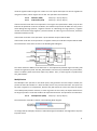
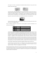
The block diagram of this ALU is as follows.
This diagram shows the relationships between the 6 operation units. The Adder/Subtractor Unit
(ASU) can perform addition or subtraction operations. The Comparator Unit (CU), which works
based on the signals from ASU, can compare two numbers and determine whether one is equal to
/ less than / less than or equal to the other. The Multiplier Unit (MU) multiplies two 8-bit numbers
and only produces the low 8-bit of the result. The Divider Unit (DU) divides one 8-bit number by
the other and produces the 8-bit quotient as well as the remainder. The Boolean Unit (BU) takes
two 8-bit numbers and performs logic AND / NAND/ OR / NOR / XOR / XNOR / “A” / NOT operations
by bit. The Shifter Unit (SU) shifts one 8-bit number by 0 to 8 bits in a direction of either left or
right, either with or without sign bit extension when shifting right.
Next we will introduce the 6 types of operations (i.e. 6 operation units) separately.
Addition/Subtraction
The Adder/Subtractor Unit operates on two 8-bit 2’s complement inputs, and generates one 8-bit
2’s complement output. That means it can operate on both positive and negative numbers, and
2
one 8-bit signed number ranges from -128 to 127. The inputs and output can also be regarded as
unsigned numbers, which range from 0 to 255. The operations are listed here.
00000
00001
Addition (ADD)
Subtraction (SUB)
ALU[7:0] <- A[7:0] + B[7:0]
ALU[7:0] <- A[7:0] – B[7:0]
If the theoretical result after some operation is too large to be represented in 8 bits, only the low
8 bits will be produced. Under this condition, the indicator output V will be HIGH. This only occurs
when adding two large positive / negative numbers or subtracting one large positive / negative
number from another large negative / positive number. In order to get correct results, overflows
should be treated seriously.
If the actual result after some operation is 0, the indicator output Z will be HIGH.
If the actual result after some operation is a negative number, the indicator output N will be HIGH.
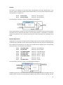
The architecture of this ASU is shown in the following block diagram.
The switch between addition and subtraction is accomplished by ALUFN0 signal and ASU_XOR
module to negate the input B. The ASU_ADD module is an 8-bit carry-lookahead carry-select adder,
which is of better performance than ripple-carry adders. The Z, V and N signals are produced by
ASU_ZVN module.
Multiplication
The Multiplier Unit operates on two 8-bit inputs, and generates one 8-bit output. Actually the
product of two 8-bit numbers is a 16-bit number, but we only save the low 8 bits. The inputs can
be either unsigned or 2’s complement, because they will lead to the same result from the aspect
of low 8-bit partial product. However, in order to get the correct results, the inputs should not be
too large to produce a result that is able to be represented in 8 bits. The operations are listed here.
00100
Multiplication (MUL)
ALU[7:0] <- A[7:0] * B[7:0]
The architecture of this MU is shown in the following block diagram.
It is simply an 8-bit multiplier, however it takes advantage of the Wallace Tree algorithm to improve
its performance.
3
Division
The Divider Unit operates on two 8-bit inputs, and generates two 8-bit outputs which is the
quotient and the remainder. Unlike the above ASU and MU, it can only handle unsigned numbers.
The operations are listed here.
00100
00101
Division (DIV)
Modulus (MOD)
ALU[7:0] <- A[7:0] / B[7:0]
ALU[7:0] <- A[7:0] % B[7:0]
The architecture of this DU is shown in the following block diagram.
The DU_DIV module is an 8-bit non-restoring divider which can produce quotients and remainders
according to input dividends and divisors. The DU_MUX module is responsible to determine
whether the quotient or the remainder should be the output according to the ALUFN0 control
signal.
Boolean Operations
The Boolean Unit operates on two 8-bit inputs, and generates one 8-bit output. Boolean operations
are bit-wise logic operations, which means that the operation and result of two corresponding bits
do not influence the vicinal bits. The result of one specific bit only depends on the corresponding
bits of the inputs. The operations are listed here.
01000
01001
01010
01011
Logic AND (AND)
Logic OR (OR)
Logic NAND (NAND)
Logic NOR (NOR)
ALU[7:0] <- A[7:0] & B[7:0]
ALU[7:0] <- A[7:0] | B[7:0]
ALU[7:0] <- ~(A[7:0] & B[7:0])
ALU[7:0] <- ~(A[7:0] | B[7:0])
01100
01101
01110
01111
Logic XOR (XOR)
Logic XNOR (XNOR)
“A”
Logic NOT (NOT)
+ B[7:0]
ALU[7:0] <- A[7:0] ○
· B[7:0]
ALU[7:0] <- A[7:0] ○
ALU[7:0] <- A[7:0]
ALU[7:0] <- ~A[7:0]
The architecture of this BU is shown in the following block diagram.
ALUFN[2:0] signals are converted into the truth values of the logic operations through the BU_FN
module, that is, the BU_FN module produces 1000 for logic AND and 1110 for logic OR, and etc.
4
Then the truth values are inputted into the BU_BOOL module together with the input numbers, to
generate the final result.
Shift
The Shifter Unit take one 8-bit number and one 3-bit number as the inputs and generates an 8-bit
output. The first number is the one to be shifted, and the second number determines how many
bits the former number is to be shifted by. Because it is meaningless for an 8-bit number to be
shifted by more than 7 bits, the second input only use the low 3 bits, and the high 5 bits are
discarded. Shifting right can be either without or with sign extension, that is, the vacant bit
positions are filled with either 0s or sign bits. To shift a number left by N bits is equal to multiply it
by 2N if the result do not overflow, and to shift a number right by N bits is equal to divide it by 2 N
(without sign extension for unsigned numbers, and with sign extension for signed numbers). The
operations are listed here.
10000
10001
10011
Shift Left (SHL)
ALU[7:0] <- A[7:0] << B[2:0]
Shift Right (SHR)
ALU[7:0] <- A[7:0] >> B[2:0] (w/o sign extension)
Shift Right Arithmetically (SRA)
ALU[7:0] <- A[7:0] >> B[2:0] (w/ sign extension)
The architecture of this SU is shown in the following block diagram.
The SX_B2, SX_B1 and SX_B0 modules are respectively responsible for shifting the 8-bit input
number by 4 bits, 2 bits and 1 bit according to the 3-bit input number. Note that the ALUFN1 signal
is to control sign extension for SR_BX modules. The SL_BX modules and SR_BX modules compose
the SU_SL module and the SU_SR module respectively. The SU_MUX module is responsible to
determine whether the left-shifted number or the right-shifted number should be the output
according to the ALUFN0 control signal.
Comparison
The Comparator Unit simply compares two 8-bit numbers and returns a 1-bit result. If the
comparison result is true, the LSB of the output is 1, vice versa. The high 7 bits of the output are
forced to be 0s. There is also one NOP instruction which produce 0x00 regardless of the inputs,
which is useful for delay. The operations are listed here.
5
11000
11001
11010
11001
Equal-To Comparison (CMPEQ)
ALU0 <- (A[7:0] == B[2:0])
ALU[7:1] <- 0x00
Less-Than Comparison (CMPLT)
ALU0 <- (A[7:0] < B[2:0])
ALU[7:1] <- 0x00
Less-Than or Equal-To Comparison (CMPLE)
ALU0 <- (A[7:0] <= B[2:0])
ALU[7:1] <- 0x00
Dummy Instruction (NOP)
ALU[7:0] <- 0x00
The architecture of this CU is shown in the following block diagram.
The ASU is forced to be in the subtraction mode when the CU is working. Thus the CU can simply
determine the results according to the Z, V and N indicator signals. The ALUFN[2:1] signals are used
to switch different comparison functions.
Testing
The key point we focused on about the self-test circuit are: 1) To cover as many types of test cases
as possible. 2) To keep the test time as short as possible.
In order to self-test all the function that is provided by the ALU with several specific test cases, all
the possible ways are as following.
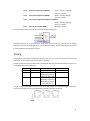
METHOD
FSM
ROM
Discrete state
Easy
Easy
FREQ DIV
Not easy
Accessibility
Relatively Easy.
Difficult to achieve
when programming
in the logic gate level.
Not easy when the
frequency need to be
divided by a number
other than the 2n
Others
Easy to maintain.
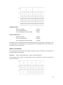
In order to get representative test cases, we use 3 state machines in cascade using asynchronous
circuit, so the status can roll up automatically, and the principle is as follows.
6
The test cases are listed in Appendix 1. After considering the two important factor of self-test, we
generate the test cases shown below, and we also plan to design the FSMs. In total, we have 3 * 3
* 19 = 171 groups of test cases, which will take 1.3486 * 171 = 231 s = 3.8 min.
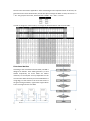
In order to design the state machine, we design the below flowchart and the truth table.
Finite State Machine
According to the work flow and truth table, the FSM is
designed as follows. Three FSMs generate A, B and
ALUFN respectively. All these FSMs are Moore
machines, so the outputs are only dependent on the
current state. When the clock pin of one FSM detects a
rising edge, its state moves to the next state. And if it
has gone through all states, it generates a signal which
is the clock signal for the next FSM.
7
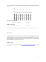
Indication
In order to give users better experiences during the self-test process, we use 7-segment and LEDs
together. The LEDs focus on showing the status of state machine A and B, which is shown as follows.
So the different status combination of LED A and B shows the status we are in among the 9 different
combinations.
A
B
On the other hand, the 7-segment is used to indicate the results of the test cases in hexadecimal
numbers.
Frequency Division
Because of the given clock is of a frequency of 50 MHz, so in order to make the frequency low
enough for human eyes to recognize the results, we divide it into 0.7415Hz using 26 two dividedfrequency D Flip-Flops in cascade.
50M / 226 = 0.7415 Hz
T = 1 / 0.7415 = 1.3486 s
The principle of two frequency divider D Flip-Flops is shown as follows.
Discussion on Improved Design
There are mainly four improved design parts in our ALU design based on the one introduced in Lab
3, that is, the carry-lookahead carry-select adder, the Wallace Tree multiplier, the 8-function
Boolean unit and the non-restoring array divider.
Carry-Lookahead Carry-Select Adder
The original design of the adder is a ripple-carry adder. It is constructed from a cascade of full
adders.
A full adder adds binary numbers and accounts for values carried in as well as out. A onebit full adder adds three one-bit numbers, often written as A, B, and Cin; A and B are the
operands, and Cin is a bit carried in from the next less significant stage. The circuit
8
produces a two-bit output, output carry and sum typically represented by the signals Cout
and S, where Sum = 2 * Cout + S. See the left graph below.
A ripple-carry adder is constructed from a cascade of full adders. Each full adder inputs a
Cin, which is the Cout of the previous adder. This is called a ripple-carry adder because each
carry bit "ripples" to the next full adder. Note that the first (and only the first) full adder
may be replaced by a half adder, or the Cin of the first full adder should be connected to
the ground. See the right graph above.
The layout of a ripple-carry adder is simple; however, the ripple-carry adder is relatively slow, since
each full adder must wait for the carry bit to be calculated from the previous full adder. Some
design are proposed to improve the propagation delay, and we implement a carry-lookahead carryselect adder.
A carry-lookahead adder works by creating two signals (P and G) for each bit position,
based on whether a carry is propagated through from a less significant bit position (at
least one input is a 1), generated in that bit position (both inputs are 1), or killed in that
bit position (both inputs are 0). In most cases, P is simply the sum output of a half-adder
and G is the carry output of the same adder. After P and G are generated the carries for
every bit position are created. See the left graph below.
In the implementation of our adder, we used two groups of 4-bit carry-lookahead adders. These
adders are provided by the Multisim master database, and are named ADD_FULL4_FCR, so we
needn’t implement for ourselves. See the right graph above.
To further improve the propagation delay of the adders, multi-bit adders can be broken into blocks.
Then the carry-select method is introduced.
A carry-select adder generally consists of two adders and a multiplexer. Adding two n-bit
numbers with a carry-select adder is done with two adders in order to perform the
calculation twice, one time with the assumption of the carry being zero and the other
assuming one. After the two results are calculated, the correct sum, as well as the correct
carry, is then selected with the multiplexer once the correct carry is known. See the left
graph below.
9
In our implementation, we use the 4-bit carry-lookahead adders as the basic adder blocks in the
carry-select configuration. Because there is no need to generate the final carry signal, the left
multiplexer is omitted.
Through the combination of carry-lookahead and carry-select method, we can get an adder of a
rather short propagation delay.
Wallace Tree Multiplier
The original design of the multiplier is an array multiplier. It is constructed from an array of AND
gates and full adders (or with some half adders).
An array multiplier works by using AND gates to produce every partial product and
summing them up. The configuration of the normal array multiplier is highly organized,
that is, one layer of AND gates followed by one layer of full adders, so it is easy to design
and manufacture. See the graph below.
However, this kind of multiplier is of much propagation delay, because the lower bits of the inputs
have to travel long distance to reach the higher bits of the output. We use the Wallace Tree
algorithm to improve the performance of the multiplier.
A Wallace Tree multiplier is an efficient hardware implementation of a digital circuit that
multiplies two integers. The Wallace tree has three steps: 1) Multiply (that is, AND) each
bit of one of the arguments, by each bit of the other, yielding n2 results. Depending on
position of the multiplied bits, the wires carry different weights. 2) Reduce the number of
partial products to two by layers of full and half adders. 3) Group the wires in two
numbers, and add them with a conventional adder. See the graph below.
10
The reduction method we use in the implementation is shown below.
Actually this is not the most typical implementation of a Wallace Tree multiplier, nor the most
optimized one. We just use this configuration because of its convenience and easy implementation.
There are still some approaches to further improving the current implementation. For example, to
optimize the layer segmentation and substitute a more efficient adder for the last layer of adders.
8-Function Boolean Unit
The original design of the Boolean unit is simply take the ALUFN signals as the truth values, and
use multiplexers to achieve different logic functions.
But this design uses 4 ALUFN signals to achieve 4 logic functions, and it is less efficient. Thus we
add one translation circuit which translate 3 ALUFN signals into the truth values. Its truth table and
logic expression is shown below.
Truth Table:
Logic
AND
OR
NAND
NOR
XOR
XNOR
“A”
NOT
ALUFN2
0
0
0
0
1
1
1
1
ALUFN1
0
0
1
1
0
0
1
1
ALUFN0
0
1
0
1
0
1
0
1
C3
1
1
0
0
0
1
1
0
C2
0
1
1
0
1
0
0
1
C1
0
1
1
0
1
0
1
0
C0
0
0
1
1
0
1
0
1
11
Logic Expression:
̅̅̅̅̅̅̅̅̅̅̅̅̅̅̅̅̅̅̅̅̅̅̅̅̅̅̅̅̅̅̅̅̅̅̅̅̅̅̅̅̅̅̅̅̅̅̅̅̅̅̅̅̅̅̅̅̅̅̅̅̅̅̅̅̅̅̅̅̅̅̅̅̅̅̅̅̅̅̅̅̅̅̅̅̅̅̅̅̅̅̅̅
̅̅̅̅̅̅̅̅̅̅̅̅̅̅̅̅̅̅̅̅̅̅̅̅̅
̅̅̅̅̅̅̅̅̅̅̅ · 𝐴𝐿𝑈𝐹𝑁1
̅̅̅̅̅̅̅̅̅̅̅ · ̅̅̅̅̅̅̅̅̅̅̅̅̅̅̅̅̅̅̅̅̅̅̅̅̅
̅̅̅̅̅̅̅̅̅̅̅ · 𝐴𝐿𝑈𝐹𝑁0 · ̅̅̅̅̅̅̅̅̅̅̅̅̅̅̅̅̅̅̅̅̅̅̅̅̅̅̅̅̅̅̅̅̅̅̅̅̅̅
̅̅̅̅̅̅̅̅̅̅̅
𝐶3 = 𝐴𝐿𝑈𝐹𝑁2
𝐴𝐿𝑈𝐹𝑁1
𝐴𝐿𝑈𝐹𝑁2 · 𝐴𝐿𝑈𝐹𝑁1 · 𝐴𝐿𝑈𝐹𝑁0
̅̅̅̅̅̅̅̅̅̅̅̅̅̅̅̅̅̅̅̅̅̅̅̅̅̅̅̅̅̅̅̅̅̅̅̅̅̅̅̅̅̅̅̅̅̅̅̅̅̅̅̅̅̅̅̅̅̅̅̅̅̅̅̅̅̅̅̅̅̅̅̅̅̅̅̅̅̅̅̅̅̅̅̅̅̅̅̅̅̅̅̅̅̅̅̅̅̅̅̅̅̅̅̅̅̅̅̅̅̅̅̅̅̅̅̅̅̅̅̅̅̅̅̅̅̅̅̅̅̅̅̅̅̅̅̅̅̅̅̅̅̅̅̅
̅̅̅̅̅̅̅̅̅̅̅̅̅̅̅̅̅̅̅̅̅̅̅̅̅̅̅̅̅̅̅̅̅̅
̅̅̅̅̅̅̅̅̅̅̅̅̅̅̅̅̅̅̅̅̅̅̅̅̅̅̅̅̅̅̅̅̅̅̅
̅̅̅̅̅̅̅̅̅̅̅̅̅̅̅̅̅̅̅̅̅̅̅̅̅̅̅̅̅̅̅̅̅̅̅
̅̅̅̅̅̅̅̅̅̅ · 𝐴𝐿𝑈𝐹𝑁1
̅̅̅̅̅̅̅̅̅̅ · ALUFN0 · 𝐴𝐿𝑈𝐹𝑁2
̅̅̅̅̅̅̅̅̅̅
̅̅̅̅̅̅̅̅̅̅ · 𝐴𝐿𝑈𝐹𝑁2
̅̅̅̅̅̅̅̅̅̅ · 𝐴𝐿𝑈𝐹𝑁0
̅̅̅̅̅̅̅̅̅̅ · 𝐴𝐿𝑈𝐹𝑁2
̅̅̅̅̅̅̅̅̅̅̅̅̅̅̅̅̅̅̅̅̅̅̅̅̅̅̅̅̅̅̅̅̅̅̅
𝐶2 = 𝐴𝐿𝑈𝐹𝑁2
· 𝐴𝐿𝑈𝐹𝑁1 · 𝐴𝐿𝑈𝐹𝑁0
· 𝐴𝐿𝑈𝐹𝑁1
· 𝐴𝐿𝑈𝐹𝑁1 · 𝐴𝐿𝑈𝐹𝑁0
̅̅̅̅̅̅̅̅̅̅̅̅̅̅̅̅̅̅̅̅̅̅̅̅̅̅̅̅̅̅̅̅̅̅̅̅̅̅̅̅̅̅̅̅̅̅̅̅̅̅̅̅̅̅̅̅̅̅̅̅̅̅̅̅̅̅̅̅̅̅̅̅̅̅̅̅̅̅̅̅̅̅̅̅̅̅̅̅̅̅̅̅
̅̅̅̅̅̅̅̅̅̅̅̅̅̅̅̅̅̅̅̅̅̅̅̅̅
̅̅̅̅̅̅̅̅̅̅̅ · 𝐴𝐿𝑈𝐹𝑁1
̅̅̅̅̅̅̅̅̅̅̅ · ALUFN0 · ̅̅̅̅̅̅̅̅̅̅̅̅̅̅̅̅̅̅̅̅̅̅̅̅̅
̅̅̅̅̅̅̅̅̅̅̅ · 𝐴𝐿𝑈𝐹𝑁1
̅̅̅̅̅̅̅̅̅̅̅
𝐶1 = ̅̅̅̅̅̅̅̅̅̅̅̅̅̅̅̅̅̅̅̅̅̅̅̅̅̅̅̅̅̅̅̅̅̅̅̅̅̅
𝐴𝐿𝑈𝐹𝑁2
𝐴𝐿𝑈𝐹𝑁2 · 𝐴𝐿𝑈𝐹𝑁0
· 𝐴𝐿𝑈𝐹𝑁0
̅̅̅̅̅̅̅̅̅̅̅̅̅̅̅̅̅̅̅̅̅̅̅̅̅̅̅̅̅̅̅̅̅̅̅̅̅̅̅̅̅̅̅̅̅̅̅̅̅̅̅̅
̅̅̅̅̅̅̅̅̅̅̅ · 𝐴𝐿𝑈𝐹𝑁1 · ̅̅̅̅̅̅̅̅̅̅̅̅̅̅̅̅̅̅̅̅̅̅̅̅̅
𝐶0 = ̅̅̅̅̅̅̅̅̅̅̅̅̅̅̅̅̅̅̅̅̅̅̅̅̅
𝐴𝐿𝑈𝐹𝑁2
𝐴𝐿𝑈𝐹𝑁2 · 𝐴𝐿𝑈𝐹𝑁0
In order to reduce propagation delay, we use reversing logic, that is, only use inverters and NAND
gates.
Non-Restoring Array Divider
There are two kinds of array divider, that is, non-restoring array divider (NRAD) and restoring array
divider (RAD). The non-restoring divider is much more efficient and faster than regular restoring
array divider. Since the array divider has many stages, it can be efficiently pipelined. More
importantly, the non-restoring divider uses a very regular structure and each cell only needs to
connect to the nearest neighbor cells, which makes it very efficient for VLSI design.
Controllable Add/Subtract Cells (CAS) are the basic building blocks of the non-restoring
array divider. It has 4 inputs and 4 outputs. P signal is to switch the function the circuit
performs. If P is 0 the CAS is a full adder, otherwise the CAS performs subtraction. S is the
result of the current bit. Cin and Cout are the carry from the less / more significant bit in
addition, or the borrow from the less / more significant bit in subtraction. See the left
graph below.
A non-restoring divider is a digital circuit that computes the quotient of two fix-pointed
numbers. The non-restoring array divider is guessing the quotient at each stage and when
it is wrong it will not correct the remainder in this stage, instead of that it would continue
to go to next stage. So it is not able to produce the correct remainder when the LSB of the
quotient is 0. Thus the extra remainder correction circuit after the last stage to correct
the last remainder output by the divider is necessary. See the right graph above. Please
refer to the Appendix for one specific example.
In order to reduce the number of the subcircuits in our PLD file, we implement the CAS as a
customized component. Thus we have to specify the SPICE model and VHDL export data. They are
shown as follows.
12
##################
SPICE Model
##################
Model ID:
CAS
Model manufacturer:
Model template:
##################
VHDL Export Data
##################
Generic
a%p [%tA?%t:d%t;A
+
%tBIN?%t:d%t;BIN
+
%tPIN?%t:d%t;PIN
+
%tCIN?%t:d%t;CIN]
+
[%tBOUT?%t:d%t;BOUT
+
%tPOUT?%t:d%t;POUT
+
%tS?%t:d%t;S
+
%tCOUT?%t:d%t;COUT] %m
Model data:
.MODEL CAS
d_chip ( behaviour= "
+; Controllable Add/Subtract
+/inputs A BIN PIN CIN
+/outputs BOUT POUT S COUT
+/table 16
+; A BIN PIN CIN BOUT POUT S COUT
+ L L L L
L L L L
+ H L L L
L L H L
+ L H L L
H L H L
+ H H L L
H L L H
+ L L H L
L H H L
+ H L H L
L H L H
+ L H H L
H H L L
+ H H H L
H H H L
+ L L L H
L L H L
+ H L L H
L L L H
+ L H L H
H L L H
+ H H L H
H L H H
+ L L H H
L H L H
+ H L H H
L H H H
+ L H H H
H H H L
+ H H H H
H H L H
+")
Export data ID: CAS
Export data manufacturer: Generic
Export data template: A
=>
%tA,
BIN
=> %tBIN, BOUT => %tBOUT, PIN => %tPIN,
POUT => %tPOUT, CIN => %tCIN, S => %tS,
COUT => %tCOUT
Export data:
library IEEE;
use IEEE.STD_LOGIC_1164.ALL;
entity CAS is
port (
A : in STD_LOGIC := 'X';
BIN : in STD_LOGIC := 'X';
PIN : in STD_LOGIC := 'X';
CIN : in STD_LOGIC := 'X';
BOUT : out STD_LOGIC := 'U';
POUT : out STD_LOGIC := 'U';
S : out STD_LOGIC := 'U';
COUT : out STD_LOGIC := 'U'
);
end CAS;
architecture BEHAVIORAL of CAS is
begin
PROCESS (A, BIN, PIN, CIN)
BEGIN
BOUT<= BIN;
POUT<= PIN;
S<= A XOR (BIN XOR PIN) XOR CIN;
COUT<= ((A OR CIN) AND (BIN XOR
PIN)) OR (A AND CIN);
END PROCESS;
end BEHAVIORAL;
Export data copyright:
Model copyright:
Then we simply implement the non-restoring array divider according to the circuit diagram.
Although non-restoring array dividers are much more efficient than restoring array dividers, they
still have long propagation delay, which will be discussed in the following section.
Performance Comparison of Improved Design
This part will show the performance comparison between the original designs and our improved
designs. We use Jsim to do the simulations and timing analyses.
Carry-Lookahead Carry-Select Adder
We compared the performance of 3 adder architecture, that is, the 8-bit ripple-carry adder, the 8bit carry-lookahead adder and the 8-bit carry-lookahead carry-select adder.
Test Cases:
Cin = { 0, 1 }
A[7:0] = { 0x00, 0x0F, 0xFF } B[7:0] = { 0x00, 0x0F, 0xFF }
The simulation result is shown in the below figure. All the 3 adders can function normally and pass
the verification.
13
Propagation Delay:
Ripple-Carry Adder
Carry-Lookahead Adder
Carry-Lookahead Carry-Select Adder
1.269 ns
1.088 ns
0.895 ns
Number of Gates Used:
Ripple-Carry Adder
Carry-Lookahead Adder
Carry-Lookahead Carry-Select Adder
48 gates
102 gates
157 gates
Therefore, the carry-lookahead carry-select adder has the best performance, but however it is of
the largest area. It is reasonable for us to implement the carry-lookahead carry-select adder if we
concentrate on the performance.
Wallace Tree Multiplier
We compared the performance of 2 multiplier architecture, that is, the 8-bit array multiplier and
the 8-bit Wallace Tree multiplier.
Test Cases:
A[7:0] = { 0x00, 0x0F, 0xFF } B[7:0] = { 0x00, 0x0F, 0xFF }
The simulation result is shown in the below figure. All the 2 multipliers can function normally and
pass the verification.
14
Propagation Delay:
Array Multiplier
Wallace Tree Multiplier
3.511 ns
1.932 ns
Number of Gates Used:
Array Multiplier
Wallace Tree Multiplier
204 gates
176 gates
Therefore, the Wallace Tree multiplier has the better performance, and its area is not larger than
the array multiplier. The area of the array multiplier is a little larger is because we do not use half
adders in the array multiplier.
8-Function Boolean Unit
We compared the performance of the 8-function Boolean unit with the original one.
Test Cases:
ALUFN[3:0] (or ALUFN[2:0]) = 0x0
A[7:0] = 0x0C
B[7:0] = 0x0A
The simulation result is shown in the below figure. All the 2 Boolean units can function normally
and pass the verification.
Propagation Delay:
Original Boolean Unit
8-Function Boolean Unit
0.190 ns
0.542 ns
Number of Gates Used:
Original Boolean Unit
8-Function Boolean Unit
24 gates
43 gates
Therefore, the 8-function Boolean unit is of a little larger propagation delay and area. However,
since the Boolean unit is not the slowest step in the whole ALU (actually, ASU, MU and DU are the
constraint steps), increment in its propagation delay will not make an influence.
Non-Restoring Array Divider
We tested the performance of the non-restoring array divider.
Test Cases:
A[7:0] = { 0x01, 0x0F, 0xFF } B[7:0] = { 0x01, 0x08, 0x88 }
15
The simulation result is shown in the below figure. The divider can function normally and pass the
verification.
Worst-Case Propagation Delay:
Non-Restoring Array Divider
18.028 ns
Number of Gates Used:
Non-Restoring Array Divider
677 gates
We can find that the propagation delay of this divider is much too long compared with other units
in the ALU. If there is no timing requirements, it is reasonable to keep this divider, otherwise the
divider has to be disposed.
Summary
In this stage of the project, we mainly focused on achieving the developing ALU and self-test circuit
design, and have implemented an ALU of mainly 19 functions while rearranging the instructions
using only 5-bit ALUFN. We have made several important improvements based on the basic design,
and also designed a totally automated self-test circuit using a cascade of 3 finite state machines.
We think we are fully prepared for the next stages!
References
Our main information source is Wikipedia (http://en.wikipedia.org/wiki/Main_Page) and 50.002
Lab 3 Handout.
16
50.002 1D Project Report
Part 2. Electronic Game Prototype
Team members: MA Ke, WEI Fanding
Introduction
In this project, we are to design and implement an educative electronic game. The second step is
to utilize the 8-bit ALU we designed in the first step to implement an electronic game prototype.
There are some other restrictions for this prototype, that is, the electronic game must be educative
and contain no more than 5 buttons. After some discussion, we decide to re-design the classic
Tetris game and implement it using 8-bit ALU on the FPGA board. Also, we are responsible to verify
the usability of the game prototype, and thus some test scenarios are necessary.
In this report, we will introduce the features of our modified Tetris game and its test scenarios, the
usage of our prototype, our design process as well as the component budget.
Game Brief
The game we decide to implement is the classic Tetris game. However, due to some limitations, we
make some simplifications on the game, and we also introduce some new features to the classic
one.
Game Description
Tetris is a tile-matching game. The classic rules are described as follows: The basic game pieces are
tetrominoes, geometric shapes composed of four square blocks each. Tetrominoes of different
shapes fall down in the playing field in a random sequence, and players can manipulate these
tetrominoes by moving each sideways and rotating it by 90 degree units. The objective is to create
a horizontal line of ten blocks without gaps, which will disappear, and any block above the
disappeared line will fall. When the stack of tetrominoes reaches the top of the playing field, the
game ends.
Due to some technical limitations, we have modified some details of the classic rules, but
maintained the whole framework of this game. The modifications can be found in the next section.
We decide to implement the Tetris game because it is very popular and educative as well. Children
are able to build tactical thinking through playing this game, as well as training their ability to react
quickly. The manipulation of this game are also easy enough to be achieved with no more than 5
buttons. Many kinds of operations are involved in the execution of this game, so we can utilize
various ALU functions.
1
Game Design
As stated above, we have made some simplifications on the classic Tetris game.
Our playing field is only 5 x 7, which means that players are to create horizontal lines of five
blocks instead of ten blocks. This is determined by the LED dot matrix we used. It is 5 x 7.
Although we can use several LED matrices as a big one, we give up this solution because that
means much heavier workload.
The basic game pieces are trominoes, which are composed of three square blocks each, rather
than tetrominoes. This is influenced by the smaller playing field. If we still use tetrominoes in
our game, players will have little space to move the pieces.
Our game do not support rotations of the trominoes. Because the new coordinates of the
blocks in one tromino are difficult to calculate, and it is hard to judge whether the new shape
will collide with the block stack or boundaries, we simply adopt this simplification. This
simplification is prone to make our game hard to continue, so we adopt an alternative way to
solve this problem, which will be introduced later. As a result, when rotations and reflections
are considered distinct, there are 6 fixed trominoes.
Only the last line is able to disappear. In order to achieve the disappearance function, we have
to add multiplexers in front of the input ports of the registers that represent the blocks in the
playing field, to select whether to maintain their original states or to fall down (on condition
that the last line disappears). Therefore if we want to make every line be able to disappear,
we have to insert many multiplexers for the registers that represents the top blocks, which is
tremendously complicated. We adopt this simplification to reduce our workload.
No fast falling down here. We think this is not an essential function, which means the game
functions normally even without this. We do not implement this function because of limited
time. However, we come up with an alternative approach to make up for this, that is, to
change the game speed.
We also introduce some new features to the classic game in order to make up for some of the
simplified functions.
Players can discard the current tromino if they do not need it. Because there is no rotation
function and only the last line can disappear, the game is prone to end in a rather short time.
Thus we come up with this discard function, which means the current tromino can be
discarded and the next tromino can be generated immediately.
Players can change the game speed themselves. Our game provides two game speed modes,
one faster and one slower. Players are able to use the faster mode if they feel bored when
waiting for the trominoes falling down.
By introducing the discard function, the modified Tetris game seems to be a little bit easy. We
believe many players can play the game endlessly. So the objective of our game is to make lines
disappear as more as possible within a limited time. Players should decide carefully whether to
utilize or to discard each tromino, in order to save time. The prototype also provides score display,
but does not provide time display yet.
2
Test Scenarios
Our test scenarios generally include two parts: basic module test and game test.
Basic module test is to verify the functions of some of the most important modules.
Tromino Generator Test: We have to test that the tromino generator module successfully
generates the correct shape type that we expected.
Key
000
001
010
011
100
101
X0
001
001
001
001
001
001
Y0
000
000
000
000
000
000
X1
000
000
001
001
000
001
Y1
001
001
000
000
001
000
X2
001
000
001
001
000
010
Y2
001
000
001
001
010
000
State Machine Test: We have to test that both of our state machines functions well, and gives
the correct outputs we expected. The tests are just to look at their outputs when a start signal
is given.
Register File Test: We should verify the functions of the two register files. The tromino register
file has 1 read port and 1 write port. The stack register file has 3 read port and 3 write port.
We test them by writing data into it and then reading data out. We also need to test the clear
function for both register files, and the remove-last-line function for stack register file.
ALU Module Test: To test the ALU functions is to ensure that the new coordinates are
calculated correctly when one behavior is specified.
F1
0
0
0
0
1
1
1
1
F0
0
0
1
1
0
0
1
1
Behavior
Down
Down
Right
Right
Left
Left
Clear
Clear
X/Y
X
Y
X
Y
X
Y
X
Y
Input
010
011
010
011
010
011
010
011
Output
110
100
011
011
001
011
000
000
Playing Field Boundary Test: To test if the judgment signal reacts as we expects when the
trominoes reach the playing field boundary. We only use one block, instead of a tromino, to
do the test.
Coordinates
000, xxx
100, xxx
xxx, 110
010, 011
Behavior
Left
Right
Down
All
Signal
0
0
0
1
Meaning
Not Movable
Not Movable
Not Movable
Movable
Stack Boundary Test: To test if the judgment signal reacts as we expects when the trominoes
reach other blocks in the stack. We only put one block in the stack.
3
Stack Block
010,110
010,110
010,110
010,110
Coordinates
011, 110
001, 110
010, 101
010, 011
Behavior
Left
Right
Down
All
Signal
0
0
0
1
Meaning
Not Movable
Not Movable
Not Movable
Movable
Register File Coupler Test: To test whether the coupler can merge two data sets from both
register files into one output data set.
LED Matrix Driver Test: To test whether the driver can convert 35 parallel inputs into 5 column
signals and 7 row signals, and drive the LED Matrix using a scan method.
Game test is to verify the behaviors of the game functions normally. The test checklist is show
below.
Step
1
2
3
4
5
6
7
8
9
10
Game Behavior
New trominoes of 6 shapes generate randomly.
The current tromino falls down automatically.
The current tromino moves left/right when left/right button is pressed.
The current tromino is discard and a new tromino is generated when
two button are pressed simultaneously.
The current tromino cannot move when there are the playing field
boundaries/other blocks in the stack blocking it.
The current tromino stays on the top of the stack when it cannot fall
down anymore, and a new tromino is generated.
The last line of the stack disappears when there are 5 blocks in it, and
all blocks above in the stack fall down.
The game restores its initial states when the reset button is pressed.
The speed switch can change the speed of the game.
The pause switch can pause and continue the game.
User Manual
This part focuses on the useful information for player to use this prototype, including a brief
introduction to the user interface and some operating instructions.
User Interface
The core interface includes one LED matrix display and two buttons on the bread board. The LED
matrix display is responsible for showing the playing field, while the two buttons are for moving
the trominoes left and right. These two buttons share the same functions with BTN0 and BTN1 on
the FPGA board.
Other axillary function buttons are on the FPGA board. BTN3 is to restart the game. SW0 is to
change the game speed. SW1 is to pause or continue. The 7-segment DISP1 is for score displaying.
Operating Instructions
Here lists some operating instructions for players. Since the basic operations are so familiar to
players, we do not need to restate them. We will focus on some special points of our Tetris game.
4
In order to restart the game, players should hold the restart button until a single point appears at
the upper left corner. Holding the button for too short or too long time will fail to restart the game.
Players can press the left or right button to move the current tromino. But players ought to prevent
pressing these buttons too frequently, or at the time when the tromino is falling down. Otherwise,
the tromino may become incomplete.
In order to discard the current tromino, players should hold left and right button until a new
tromino is generated.
Toggling the pause switch is to pause the game. Toggling again is to continue.
Toggling the speed switch is to change the game speed. There are two speed mode. In the fast
mode, the trominoes fall down every 0.67 second, while in the slow mode, they fall down every
1.34 second.
Design Process
Since the Tetris game is quite complicated to implement, we divide the whole task into some small
tasks, and work them out one by one. We also make several design decisions in the process and
solve some problems.
Steps in Building the Prototype
Step 1: Tromino Generation. We used a 3 bit key value to represent the shapes because there are
only 6 distinct shapes as follows. To randomly generate the 6 distinct shapes, we use three modules
to achieve this.
Key Value
Tromino Shape
Key Value
000
011
001
100
010
101
Tromino Shape
1) Pseudo-random number generator: we adopt the linear feedback shift registers method to
generate pseudo-random number. The advantages of this method are simple construction,
long cycle and good randomness. The diagram of an m-stage LFSR is shown below, where
factor fi = 1 means close connection and fi = 0 means open connection.
5
2) Number filter: Because there are only 6 shapes, the shape is undetermined if the generator
has generated the key value 110 or 111. So we use a filter to replace 110 with 100, and 111
with 001. It is easy to achieve it by a combinational logic unit.
3) Tromino coordinate generator: When the key value has been decided, it is easy to decide
the x and y coordinates of each block in the tromino. Because there are only 7 rows and 5
columns, both x and y coordinates can be represented with 3-bit numbers. So in total, we use
an 18-bit code to represent those 3 blocks. The 18-bit code is composed as follows.
XA2
XA1
XA0
YA2
YA1
YA0
XB2
XB1
XB0
YB2
YB1
YB0
XC2
XC1
XC0
YC2
YC1
YC0
Step 2: Tromino Loading. We can get a randomly generated tromino through the last step, and we
also need to store it for further calculations. We develop a tromino register file for storing the
coordinates, and a state machine to put the generated coordinates into the register file.
1) Tromino register file: This register file contains 18 flip-flops to save the 18-bit code. We also
implement one read port, which outputs data through RD according to the input address RA,
and one write port, which write data from WD into the given address WA. All above data and
addresses are 3-bit, which is enough for our game. The low-order 2 bits of the addresses are
for block selecting, that is, 00 is corresponding to block A in the tromino, 01 to block B and 10
to block C. 11 is not used. The high-order 1 bit of the addresses are for X/Y selecting, that is,
0 is corresponding to X coordinate and 1 to Y. An asynchronous clear port is for flushing the
register file when the game restarts. There are also 18 parallel outputs which are fed into
register file coupler for displaying.
2) State machine A: The state machine has 6 states. When it gets a rising edge from its start
port, it starts to run the 6 states one by one for 1 time. The outputs of the state machine is 3bit WA. For each state, we choose 3-bit WD from the generated x and y coordinates of the 3
blocks using 3 multiplexers according to WA. Then WA and WD are fed into the tromino
register file to store the tromino coordinates.
Step 3: Boundary Judgment. The current tromino cannot move any further if there are playing field
boundaries or other blocks in the stack blocking it. Boundary judgment is to calculate the
coordinates of the new position if the current tromino moves down/left/right one more time, and
examine whether the new coordinates exceed the playing field or collide with other blocks in the
stack. In other words, we calculate 3 reference blocks for each block in the tromino, and use them
for boundary judgment through the following judgers.
1) Playing field boundary judger: To examine whether the current tromino reaches playing
field boundaries. It may reach the bottom boundary like the left graph below, or the left/right
boundary like the right graph below. This judgment is done by simply comparing the
coordinates of the reference blocks with the playing field boundaries. If one of the x
coordinates of the left reference blocks is 111 (-1), the current tromino cannot move left. If
one of the x coordinates of the right reference blocks is 101 (5), the current tromino cannot
6
move right. If one of the y coordinates of the bottom reference blocks is 111 (7), the current
tromino cannot move down.
2) Stack boundary judger: To examine whether the current tromino reaches places where its
adjacent blocks have already been taken. For example, the current tromino cannot move left
or down in the below condition. This judgment is done by feeding the coordinates of the
reference blocks corresponding to one specific behavior, into the read ports of the stack
register file, and check the outputs to see whether these blocks are already taken.
3) Synthesized boundary judger: The final judgment signal for all three behaviors are the union
of the above two judgment signals.
Step 4: Coordinate Operations. We use the F1 and F0 signals to choose the behaviors. The
processes are listed below.
F1
0
0
1
1
F0
0
1
0
1
Behavior
Fall Down
Move Right
Move Left
Discard
ALU Operation
ADD 1 to yA, yB, yC
ADD 1 to xA, xB, xC
SUB 1 from xA, xB, xC
AND 0 with xA, xB, xC, yA, yB, yC
1) Data path: When both buttons are not pressed, F1 and F0 are acquiescently 00, so the
tromino coordinates are calculated assuming falling down behavior. Once the left or right
button is pressed, F1 and F0 will simultaneously change so that the tromino coordinates are
calculated in moving left/right mode. When both of the buttons are pressed, F1 and F0 will
change to 1 together, so the discarding behavior will be executed. It flushes the tromino
register file and generates a new tromino. The four behaviors are chosen by F1 and F0 signals
and executed by ALU. When the coordinates of the blocks have been calculated by ALU, they
will be written into the tromino register file again. The write addresses are the same as the
read addresses in the same clock period. Of course, whether the new coordinates should be
written again is determined by the boundary judgment signal we get in the last step.
2) State machine B: This state machine is for reading the x and y coordinates of the tree blocks
from the tromino register file one by one, and writing the calculated coordinates into the
register file again. It accepts a rising edge as the start signal.
Step 5: Block Accumulation. When the current tromino falls down and reaches the top of the stack,
it cannot fall down any further, so the coordinates should be saved into the stack register file from
the tromino register file. When the last line is complete in the stack register file, it should disappear
and blocks above should fall down.
7
1) Stack register file: This register file is a 2D register file containing 5 x 7 flip-flops. Three read
ports and three write ports are provided. When a 3-bit RA is specified, the 1-bit RD output
shows whether the corresponding block has been taken. When a 3-bit WA is specified and the
WE is enabled, the state of the corresponding register changes to 1. An asynchronous clear
port is for flushing the register file when the game restarts. There are also 35 parallel outputs
which are fed into register file coupler for displaying. In order to achieve the disappearing
function, we implement a circuit to check the status of the registers in the last row. When they
are all 1, the circuit gives a RM signal. This signal is fed into the multiplexers in front of the
registers, which are to choose whether to maintain the current state or to fall down.
2) Write control signal: When the falling down judgment signal becomes 1, it tells us that the
current tromino cannot fall down anymore. Then the WE signal for the stack register file will
become 1, and the parallel outputs of the tromino register file are fed into the WA ports of
the stack register file. So the blocks of the tromino register file are saved into the stack register
file after next clock tick. This signal is also responsible to generate a new tromino.
Step 6: Result Display. We have to display the data from both the tromino register file and the stack
register file on one LED dot matrix. Also we need to use 7-segment to display the number of lines
disappeared.
1) Register file coupler: The parallel outputs of the tromino register file are binary values
indicating the coordinates of the blocks in the tromino. The parallel outputs of the stack
register file are Boolean values indicating whether the blocks are occupied. To merge these
two types of data, we should first convert the coordinate data into 2D Boolean data using 2D
decoders, and then do the logic or operations on every block.
2) LED matrix driver: In order to scan every row, we use a circular counter as the state machine.
The outputs of the counter are decoded and served as row selecting signals. Column signals
are generated through selecting the inputs using multiplexers according to the current row
selecting signals.
3) Score counter: The RM signal from the stack register file serves as the ENT signal for the
score counter. The score counter should be synchronized with the stack register file. So every
time the last line disappears, the counter increments by 1. The outputs of the score counter
are decoded and connected to the 7-segment inputs.
Step 7: Clock Generation. There is only one clock on the FPGA board, and it is quite fast. We have
to utilize it to generate several slower clocks of different frequency for various purposes. We use
three clocks in the game: progress clock, operation clock and scan clock. We also implement the
pause/continue and speed change functions.
1) Frequency divider: We implement the frequency divider with a classic method that uses a
cascade of D flip-flops. Clocks of different frequencies can be obtained from the outputs of
the flip-flops.
8
2) Pause/continue and speed change functions: The progress clock represents the game speed
that players can really feel. So we change the progress clock to set different difficulties using
a multiplexer. On the other hand, if we force the clock to 0, the states will not change anymore,
so the game stops to execute. Thus it can be regarded as a pause function.
Design Issues
Issue 1: The block sequence in a tromino.
The sequence of the blocks is decided by the following rules. For the blocks in different rows,
the blocks of the lower row numbers will be counted first. For the blocks in the same row, the
blocks of lower column numbers will be counted first. According to these rules, the following
shapes will be counted like this:
Thus we can generate tromino coordinates according to the key value in the following way:
Firstly, the coordinate (xA, yA) is fixed as (010, 000). Then we can generate the second and the
third block coordinate based on the key value. This is easy to be achieved by combinational
logic unit.
Issue 2: Proper data capacity.
Although our ALU is 8-bit, due to our small playing field, all of the data can be represented
within 3 bits. So we decide to use the 3-bit standard. The high-order 5 bits of the ALU inputs
are forced to 0. Also the addresses and data for the register files are 3-bit.
Issue 3: Switch between generating new trominoes and moving current trominoes.
Generating new trominoes and moving current trominoes both require the access to the
tromino register file. So we use multiplexers to switch between these functions, but the
selecting signal should be carefully design.
Generating new trominoes occurs in three situations: the game restarts, the current tromino
has been discarded or the current tromino has reached the stack top. On all other conditions,
moving current trominoes function should execute or waiting for executing. Note that all the
situations that generating new trominoes executes will invoke a start signal for the tromino
generator. Thus the selecting signal can be associated with the start signal, and holds for
several clock periods until the new tromino is stored in the tromino register file.
Issue 4: Tradeoff between ALU and independent calculation circuits.
We have to make some design decisions whether to use ALU or independent calculation
circuits. Because many operations are involved in this game, we have to consider the
situations separately.
The advantage of using ALU is to save some logic gates. However, we have to add many
multiplexers and construct a much more complex data path. Because we can only use one
ALU, the operations are executed sequentially, which requires more clock cycles.
9
The advantage of using independent calculation circuits is to simplify the data path and reduce
the calculation time. By using multiple independent calculation circuits, we can make some
operations parallel.
So we finally decide to only use ALU for coordinate calculations, which only needs 6 clock
cycles. The calculations of reference blocks and boundary judgments are done by independent
calculation circuits and made parallel.
Issue 5: Clock frequencies used.
We use three clocks of different frequencies in our game, that is, progress clock, operation
clock and scan clock.
The slowest clock is the progress clock. It is used for controlling the time when the current
tromino should fall down as well as the stack register file. This frequency is the only one that
players are aware of. The change of the game speed is also to change this clock.
The medium clock is the operation clock. It is used for the state machines and the tromino
register file. One progress clock cycle must contain at least six operation clock cycles in order
to calculate the new coordinates for falling down behavior. However, taking moving left/right
into consideration, the progress clock cycles should be much longer than the operation clock
cycles. When the left or right button is pressed at the time when the coordinates for falling
down behavior are being calculated, the current calculation will be interrupted and a new
calculation will start. This will cause bugs like incomplete trominoes. In general, the higher the
ratio of operation clock frequency to progress clock frequency, the less possibilities of
exceptions.
The fastest clock is the scan clock. It is used only for LED matrix driver. Its frequency must be
higher than 25 x 7 = 175 Hz to prevent players from being aware of the scanning process. The
actual scan clock frequency is much higher.
Issue 6: Sequential issues.
The game involves many sequential issues. For example, some modules should accept a start
signal and wait for another several clock cycles to start. Under these circumstances, we use
some cascades of flip-flops to achieve the delay function. The specific details are omitted here.
Implementation Problems
Actually, the above parts are the outcomes after we have solved numerous problems; most of the
problems have already been covered. So this part we will focus on some unsolved problems and
propose some solutions.
Problem 1: The restart sequential logic should be re-designed. Now whether the restarting succeed
or not depends on the time players hold the restart button. Actually this is not user-friendly.
However, improving this is difficult because we need a signal to be 0 for a short period and then to
be 1. A possible solution may be introducing a mono-stable circuit.
Problem 2: The discard button should be held for a period to discard the current tromino. This
problem is quite similar to the former one. A mono-stable circuit may resolve this.
10
Problem 3: The trominoes sometimes become incomplete. This occurs when one calculation is in
progress and another calculation starts. That is, when players press the left/right button too
frequently or press any of them at the time when the tromino is about to fall down, the tromino is
prone to be incomplete. The solution may be to block other signals when one calculation is in
progress.
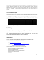
Component Budget
The most important part of our Tetris game is based on the FPGA board; the external circuit is only
for displaying and operating. The FPGA board and breadboarding wire bundle are provided by
computer lab. Thus the component budget for our game is actually quite low. The detailed
information is listed below.
Component Name
Breadboard Medium Self-Adhesive, 640 tie-in points
LED Dot Matrix 5x7 Orange 18mm Anode
Momentary Push Button Switch - 12mm Square
Resistor, Carbon Film, High Stab, 0.25W, 5%, 1k
Unit Price
$6.90
$3.80
$0.80
$0.05
Quantity
1
1
2
1
Total Price
$6.90
$3.80
$1.60
$0.05
Thus the total cost is approximately SGD 12.35.
Summary
In this stage of the project, we mainly focus on developing the electronic game prototype, that is,
a modified version of the classic Tetris game, which we believe is educative to children. We
implement this prototype with 3 buttons and 2 switches, and utilize 3 ALU functions. We think
what we have accomplished satisfies the project requirements well. The design and
implementation details are described in this report for reproducing.
References
Our main information source are Wikipedia, 50.002 handouts and an academic paper.
The main reference entries in Wikipedia are listed below:
Tetris: http://en.wikipedia.org/wiki/Tetris
Frequency Divider: http://en.wikipedia.org/wiki/Frequency_divider
Dot Matrix: http://en.wikipedia.org/wiki/Dot_matrix
The main reference slides in 50.002 handouts are listed below:
Lecture Note 4: Synthesis of Combinational Logic
Lecture Note 5: Sequential Logic
Lecture Note 6: (Synchronous) Finite State Machine
Lecture Note 14: Building the Beta
Lab 6: Beta
11
Other reference is:
SHU Li-bao, SONG Ke-zhu, and WANG Yan-fang. The Implementation and Research on Pseudo
Random Number Generators with FPGA. Journal of Circuits and Systems 8.3 (2003): 121-124.
12