1
Using BSDL for Board-level Testing
The appearance of ”linkage” in a pin’s file implies that the pin cannot be used with boundary scan. These
are usually power pins or analog pins that cannot be defined with a digital logic state.
10.5
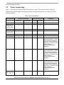
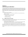
Boundary scan operation
The boundary scan operation is controlled by:
•
•
BOOT_MODE0, BOOT_MODE1, and JTAG_MOD pins
On-chip Fuse bits
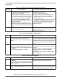
The JTAG_MOD pin state controls the selection of JTAG to the core logic or boundary scan operation.
See the following references for further information:
• The “System JTAG Controller (SJC)” chapter in the chip reference manual for the definitions of
the JTAG interface operations.
• The “JTAG Security Modes” section in the same chapter for an explanation of the operation of the
e-Fuse bit definitions in the following table.
• The “Fusemap” chapter in the chip reference manual the fusemap tables.
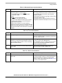
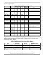
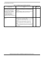
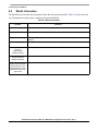
Table 10-1. System considerations for BSDL
Pin name
JTAG_MOD
BOOT_MODE[1:0]
POR_B
Logic state
1
[0:0]
[0:1]
[1:0]
1
Description
IEEE 1149.1 JTAG compliant mode
Boot From Fuses
Serial Downloader
Internal Boot (Development)
Power On Reset for the device
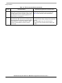
e‐Fuse bits
JTAG_SMODE[1:0]
SJC_DISABLE
10.6
[0:0]
[0:1]
0
JTAG enable mode
Secure JTAG mode
Secure JTAG Controller is enabled
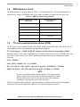
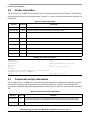
I/O pin power considerations
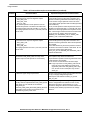
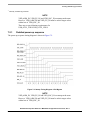
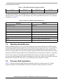
The boundary scan operation uses each of the available device pins to drive or read values within a given
system. Therefore, the power supply pin for each specific module must be powered in order for the IO
buffers to operate. This is straightforward for the digital pins within the system.
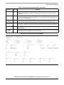
NOTE
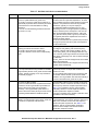
BSDL was only tested at 1.8 V.
Hardware Development Guide for i.MX 6SoloLite Applications Processor, Rev. 1
10-2
Freescale Semiconductor