1
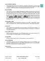
The PLL maximum lock time is determined by the input clock to the phase detector.
The PLL locks within 500 input clock cycles.
NOTE
Upon initial system power up and after KAPWR is lost, an external
circuit must assert power on reset (PORESET). If limp mode will be
enabled during power-on reset, PORESET must be asserted for at
least 100,000 cycles of input PLL clock after a valid level has been
reached on the KAPWR supply. If limp mode will be disabled,
PORESET should be asserted for approximately 3 µs after a valid
level has been reached on the KAPWR supply.
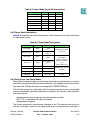
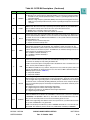
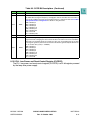
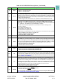
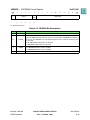
Whenever power-on reset is asserted, the MF bits are set according to Table 8-1, and
the DFNH and DFNL bits in SCCR are set to the value of 0 (÷1 and 2), respectively.
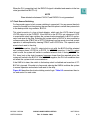
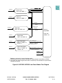
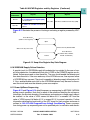
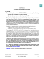
XFC
OSCCLK
Division Factor
DIVF[0:4]
Feedback
Phase
Comparator
Up
Down
System
Frequency
(FREQSYS)
Charge
Pump
VCO
÷2
VDDSYN / VSSSYN
÷2
Clock
Delay
Multiplication Factor
MF[0:11]
Figure 8-3 System PLL Block Diagram
8.3.5 PLL Pins
The following pins are dedicated to the PLL operation:
• VDDSYN — Drain voltage. This is the VDD dedicated to the analog PLL circuits.
The voltage should be well-regulated and the pin should be provided with an extremely low impedance path to the VDD power rail. VDDSYN should be bypassed
to VSSSYN by a 0.1 µF capacitor located as close as possible to the chip package.
• VSSSYN — Source voltage. This is the VSS dedicated to the analog PLL circuits.
The pin should be provided with an extremely low impedance path to ground.
VSSSYN should be bypassed to VDDSYN by a 0.1 µF capacitor located as close
as possible to the chip package.
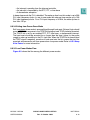
• XFC — External filter capacitor. XFC connects to the off-chip capacitor for the
PLL filter. One terminal of the capacitor is connected to XFC, and the other terminal is connected to VDDSYN.
The off-chip capacitor must have the following values:
MPC555 / MPC556
CLOCKS AND POWER CONTROL
USER’S MANUAL
Rev. 15 October 2000
MOTOROLA
8-5