1
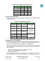
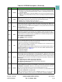
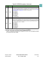
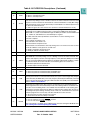
Table 8-1 Reset Clocks Source Configuration
Default Values @ PORESET
1
MODCK[1:3]
LME
000
SPLL Options
MF + 1
PITCLK
Division
TMBCLK
Division
0
513
4
4
Used for testing purposes.
001
0
1
256
16
Normal operation, PLL enabled.
Main timing reference is freq(OSCM) = 20 MHz.
Limp mode disabled.
010
1
5
256
4
Normal operation, PLL enabled.
Main timing reference is freq(OSCM) = 4 MHz.
Limp mode enabled.
011
1
1
256
16
Normal operation, PLL enabled.
Main timing reference is freq(OSCM) = 20 MHz.
Limp mode enabled.
100
101
0
1
256
16
Normal operation, PLL enabled. 1:1 Mode
freqclkout(max) = freq(EXTCLK)
Limp mode disabled.
110
0
5
256
4
Normal operation, PLL enabled.
Main timing reference is freq(EXTCLK) = 3-5 MHz.
Limp mode disabled.
111
1
1
256
16
Normal operation, PLL enabled. 1:1 Mode
freqclkout(max) = freq(EXTCLK)
Limp mode enabled.
NOTES:
1. For other implementations in the MPC500 family, MODCK2 could be inverted.
NOTE
The reset value of the PLL pre-divider is 1.
The values of the PITRTCLK clock division and TMBCLK clock division can be
changed by software. The RTDIV bit value in the SCCR register defines the division
of PITRTCLK. All possible combinations of the TMBCLK divisions are listed in Table
8-2.
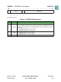
Table 8-2 TMBCLK Divisions
SCCR[TBS]
MF + 1
TMBCLK
Division
1
—
16
0
1, 2
16
0
>2
4
8.6.1 General System Clocks
The general system clocks (GCLK1C, GCLK2C, GCLK1, GCLK2, GCLK1_50, and
GCLK2_50) are the basic clock supplied to all modules and sub-modules on the
MPC555 / MPC556. GCLK1C and GCLK2C are supplied to the RCPU and to the BBC.
GCLK1C and GCLK2C are stopped when the chip enters the doze-low power mode.
GCLK1 and GCLK2 are supplied to the SIU and the clock module. The external bus
clock GCLK2_50 is the same as CLKOUT. The general system clock defaults to VCO/
MPC555 / MPC556
CLOCKS AND POWER CONTROL
USER’S MANUAL
Rev. 15 October 2000
MOTOROLA
8-9