1
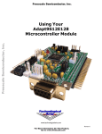
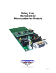
Using Your Adapt9S12XDP Microcontroller Module
| Print |
Introduction
An enhancement of the popular HCS12 family (and fully backward compatible CPU), the S12X family utilizes the latest process technology. It boasts
higher speed (40 MHz), more functionality, reduced power consumption and cost, and enhanced performance with the XGATE RISC coprocessor,
on-chip memory-management and DMA module. Adapt9S12XDP512 is a modular implementation that brings these advantages within easy reach of
engineers, educators, and hobbyists. The flexible design of the "Adapt" series of microcontroller products addresses all aspects of training, evaluation,
development, prototyping, and even volume production.
This manual provides basic setup and operation instructions for the Technological Arts Adapt9S12XDP Microcontroller Module. Included are both the
hardware and software information needed to get the board working with a variety of programming languages and development tools. You can use
assemblers and languages such as C, Forth, and Basic. Debugging can be accomplished by using the built-in serial monitor and an external program,
such as uBug12 Java Edition, or by use of a BDM pod.
Overview of features
The Adapt9S12XDP microcontroller module comes equipped with a variety of interfaces and on-chip resources. These include, but are not limited to,
the following:
- Maximum bus speed: 40 MHz for S12X CPU, 80 MHz for XGATE coprocessor.
- Memory resources: 512 KB Flash, 4 KB EEPROM, 32 KB RAM
- Operating voltage: either direct 5 VDC at 100 mA, or 6-12 VDC at 150 mA
- Communications interfaces: two RS232C, two CAN, and one RS485
- User LED: red LED on Port P bit 7 available for application use.
- On-chip serial monitor: adaptation of popular Freescale AN2548 serial monitor programmed into top 2 KB of Flash. This has been specially modified
for use on the S12XDP CPU.
- Factory-installed Demo program: demonstrates some of the Adapt9S12XDP module capabilities.
- BDM connector: this 10 pin standard header connector allows the use of a separate BDM pod for debugging programs in real-time, and for
programming all Flash and EEPROM memories. Supports 6-pin and 10-pin BDM pods.
- Expansion connectors: these two 50-pin standard connectors enable additional external hardware to be connected to the board.
Getting Started
The first step in preparing to use the module is to read through this manual, before attempting to apply power to the device. Next, verify that the power
cable is present. It plugs into a matching two-pin connector on the board. There should also be a schematic of the board, and a pinout guide for the two
50 pin expansion headers on the board.
WARNING: The board contains electrostatic sensitive components, and it is recommended that standard electrostatic precautions be taken when
handling the module. There does not have to be a visible spark for a dangerous voltage to affect the electronics. Just walking accross a carpet on a
dry day is enough to build up a potentially damaging amount of static charge. Recommended precautions include using a wrist grounding strap
and/or a grounded workstation. The module can also be installed in a protective housing to keep it isolated from undesired external voltage sources.
Setup and Verification of Hardware
Power and serial connections, switch positions, default jumper positions
If you have purchased a bundle (i.e. an Evaluation Package or Solderless Experimentor Package), a suitable power supply is included. Otherwise, the
power cable assembly #PCJ1-8, supplied with the board, can be used to connect to your external power source. The tinned ends of the cable assembly
can be connected to a bench power supply, spliced onto the cut-off end of a power supply, connected to a battery pack, or used in some other
arrangement which you find suitable for your application. The board requires a DC power source capable of delivering between 6 and 12 volts at a
minimum of 150 mA. Most standard "brick" power supplies should be capable of meeting this requirement. If you need to purchase one, Technological
Arts offers a suitable choice for North American customers:
1. #DC9V, a 9V 300mA North American style wall adapter, which has a 2-pin Molex connector, ready to attach to the board's power connector
Additional power cables are also available if needed. Item #BJ2PCJ1 includes a barrel jack to connect to the barrel plug of an unmodified wall adapter.
Once the power cable has been attached to your power supply, use a voltmeter to verify that the red wire is in the +6 to +12 DC volts range in relation
to the black (ground) wire. Only then should the cable be plugged into the matching two-pin power connector on the board. (Refer to the diagram
below.) When power is first applied, the green LED on the board should light up. This provides verification that the module is receiving power. Unplug
power before proceeding.
There is a slide switch on the board, labelled as Load/Run. This is used to select between booting up with the serial monitor (Load), and a user
installed application (Run) when power is first applied or whenever the Reset button is pressed. The Reset button is a small momentary contact switch
at one edge of the board, opposite from the power connector.
There are several jumpers placed on the board as well as pads to put jumpers. When the board is first used, there are only a couple of jumpers that
need to be checked. These are listed below, along with their default settings. (A full jumper list is provided later.)
Jumper
Function
Default Setting
JB1
ModA select
0 hard-wired
JB1
ModB select
0 hard-wired
SW2
Load/Run to PA6
Run
These should generally be left at their default settings, unless there is an application need to change it. The ModA and ModB settings select Single
Chip mode, which is the only mode the M9S12XDP512 is designed to be used in with this module. A BDM pod will use Special single chip mode, but
that still requires ModA and ModB stay at these settings.
The 9-pin D-sub connector on the board is a standard RS232 serial port implemented on SCI0 on the S12X chip. SCI1 is also implemented as an
RS232 port, next to the 9-pin D-sub, as a four pin header. The board includes an RS232 level translator for both of these, so the output can attach
directly to a serial port on your computer. Technological Arts provides a cable (Item #SCPC9) for SCI1 that plugs into the header and provides a
standard 9-pin D-sub connector, just like SCI0. The pinouts for these two serial connectors are as follows:
SCI 0
Pin 2
Pin 3
Pin 5
Description
Transmitter Output
Receiver Input
Ground
SCI 1
Pin 1
Pin 2
Pin 3
Pin 4
Description
Receiver Input
Ground
Transmitter Output
+5 Volts
You will need a serial cable for the 9-pin SCI0 connector if you plan to use the pre-installed serial monitor to program the board and troubleshoot your
applications. This is also used by the Demo program that comes programmed in Flash.
Using the Factory-Installed Demo Program
The Adapt9S12XDP module comes programmed with a Demo program in Flash. You can run this with the Load/Run switch in the Run position when
applying power or pressing reset. When the program starts, it will blink the red LED on Port P7 three times, to show that it is running. To use the
program though, you will need to connect a serial cable from the SCI0 serial connector to your computer. The Demo program requires use of an ASCII
terminal program, like HyperTerminal on Windows systems, to provide a means for you to interact with the program. The terminal program will need to
be set up with the following properties:
Emulate ANSI terminal type
115200 baud
8 bits
One stop bit
No parity
No flow control
Do not append line feeds in incoming line ends
No local echoing of typed characters
When the Demo program starts, it prints out a menu as follows:
Adapt9S12XDP512 DEMO PROGRAM COMMAND MENU V1.00
_________________________________________________
A
B
C
E
F
H
J
K
M
P
S
T
=>
=>
=>
=>
=>
=>
=>
=>
=>
=>
=>
=>
SHOW PORT A STATUS
SHOW PORT B STATUS
CLEAR PORT P OUTPUTS
SHOW PORT E STATUS
FLASH LED (CONNECT TO PP7)
SHOW PORT H STATUS
SHOW PORT J STATUS
SHOW PORT K STATUS
SHOW PORT M STATUS
SHOW PORT P STATUS
SHOW PORT S STATUS
SHOW PORT T STATUS
R => SHOW 10 BIT REAL-TIME ANALOG VALUES
0 TO 7 => TOGGLE THE SELECTED P PORT LINE
?
Typing each of the available letter commands in sequence from A through R may generate output similar to the following:
PORTA=255
PORTB=000
PORT P CLEARED
PORTE=159
>>> LED FLASH! <<<
PTH=000
PTJ=247
PORTK=255
PTM=015
PTP=000
PTS=255
PTT=000
AD0=0384 AD1=0390 AD2=0391 AD3=0385 AD4=0384 AD5=0384 AD6=0384 AD7=0387
The analog output updates the same line continuously on the screen. You can terminate the update with the Enter key, which will reprint the menu.
The number keys 0 through 7 will toggle the level value for the corresponding pin on Port P. You can see this by typing 7, and watching the red LED on
the board change state.
Application Programming
There are several language options available for writing application programs for the Adapt9S12XDP module. One can use Assembler, C, Basic, Forth,
or a combination of these. This section will list descriptions and hardware specific setup instructions for the various systems available. The choice of
what to use is left to the user. Generally though it will be based on application requirements, budget, and what the programmer is familiar with or willing
to learn.
Many of the language options available will require the use of uBug12 to program the generated S-records into the S12X Flash memory. uBug12 is
also usful for real-time debugging when a BDM pod is not available. You can find instructions on how to download and use uBug12 at this URL:
http://www.technologicalarts.ca/shop/documentation/63-debugging-tools/171-ubug12je-user-manual.html
Keep in mind that there is a difference between a programming language and an Integrated Development Environment (IDE). An IDE combines several
functions of the development process into one program. It can be designed to work with a specific language, like C or Forth. However the language
does not define the IDE functionality. An IDE can include an editor, assembler, compiler, simulator, debugger, serial monitor interface or BDM pod
interface, or some subset of these capabilities. It will depend upon the IDE. So review what each can do before choosing one to work with. An IDE can
be useful because it can combine several development steps into one, or allow blending of the functions. (i.e. Source level debugging, or using both
assembly and the featured language.)
Another important factor to remember are the differences between the S12X CPU and its predecessor, the HCS12. There is much software written for
the HCS12, and you can still find many boards available that use the MC9S12DP256 processor, its most common variant. The two processors are
code compatible, so it is theoretically possible to write code on for the HCS12 and have it run on the S12X. However there are some critical differences
between the two environments. Here are a few of the more important ones:
The HCS12 instruction set is a subset of the S12X. There are no Global addressing instructions, for example. You will need to review the
Freescale manual on the S12X for a full list of the differences, as there are many new instructions.
The HCS12 has no XGATE coprocessor.
The HCS12 based hardware has registers that are not in the S12X, like INITEE, etc.
The S12X has registers that are not in the HCS12, for example EPAGE and RPAGE which are used for accessing banked EEPROM and RAM
respectively.
The PPAGE register, which is used to select the Flash bank seen at $8000-$BFFF, has different allowed values. The HCS12 for the 256K Flash
only allowed $30-$3F. The 512K S12X uses $E0-$FF instead.
What this means is that there are development environments available (IDE) and debugging tools that were written for the HCS12 and might be used
for the S12X, but with limitations. The most obvious indication of this will be if the IDE or programming language states that it uses the as12 assembler,
which was written for the HCS12, not the S12X. Debugging tools for the HCS12 will have to be considered carefully, as they may not be compatible
enough to work with the S12X due to the hardware differences. Of course this also means that if you have to migrate code from the HCS12 to the
S12X, you will need to check that the source is modified to take these differences into account.
To assist you in getting a better idea of what is available, here is a table of the major development platforms that are available, and that can be used to
develop software for the Adapt9S12XDP:
Language
Assembler
IDE
XGATE
CodeWarrior Special
C
S12X/XGATE
x
CodeWarrior Pro
C
S12X/XGATE
x
Serial Com
BDM Com
Other
x
x
32K for C
x
x
commercial product
FIG-Forth
HSW12
AsmIDE
MiniIDE
SBASIC
GCC-Syncode
GCC-Eclipse
Imagecraft C
Cosmic C
Forth
Assembler
Assembler
Assembler
BASIC
C
C
C
C
S12X/XGATE
S12X/XGATE
S12X/XGATE
as12
as12
as12
as12
as12
S12X/XGATE
x
x
x
x
x
x
x
Linux
x
limited assember
limited assember
limited assember
limited assember
limited assember
commercial product
x
x
x
All of these will work with an assembler, and allow assembly code to be embedded within the language. The main difference will be in what assembler
is used. There are several S12X/XGATE assemblers available that can be used to write software: Code Warrior from Freescale, Cosmic Software's
cas12x (part of their C programming environment), and Dirk Heisswolf's HSW12. Each of these come with their own IDE programs as well. There are
other assemblers that are compatible, but these were written for earlier processor versions in the HC12 line. As a result, they do not cover the full
instruction set of the S12X, but only a subset of it, and are therefore not covered in detail here.
What follows are brief descriptions, and instructions where needed, for each of these development tools.
CodeWarrior
CodeWarrior is considered the industry standard, and is available in different suites from Freescale. Each suite has different capabilities and prices.
The least expensive of these is the Special suite, and is available for free. Its main limitation is that it only allows C programs to compile to a maximum
size of 32 KB. The assembler is not bound by this limitation though. On the other end of the suites is the Professional version. CodeWarrior includes an
IDE and a simulator. You can find out more by visiting the Freescale site for CodeWarrior at:
http://www.freescale.com/webapp/sps/site/prod_summary.jsp?code=CW-HCS12X&fsrch=1
You will find a link on this page to download the Special suite of the software. The link will download an executable to run that does the actual
installation. Please be aware that the file size is over 300 MB, so it is best to use the fastest network connection possible. However you can also order
a CD to obtain the software.
Here are some other links for documentation to help get CodeWarrior up and running. This is a comprehensive, and therefore complex, package. Plan
to spend some time learning how to use it.
CodeWarrior Documentation List
Quick Start Instructions
Compiler Documentation
CodeWarrior Development Tools Learning Center
If you plan on using CodeWarrior to do interactive debugging with your hardware, you will need a BDM pod that is compatible with CodeWarrior. It is
not guaranteed to work with any BDM, nor will it work via a serial monitor interface. (Compatible BDM pods are listed in the Freescale documentation.)
However it will generate S-records that can be programmed into a target module via the serial monitor and uBug12x.
Dirk Heisswolf's HSW12
This S12X/XGATE assembler is part of Dirk Heisswolf's HSW12 IDE. This is a freeware IDE and assembler available on the web. (The site is listed in
the instructions to follow.) The main difference with this development platform from others is that it is designed to be run on Linux systems. The IDE is
also designed to work with a BDM pod when loading and debugging programs. However the assembler itself can easily be made to run on Windows
computers, with the additional installation of a Perl interpreter, which is also freely available.
Here are the instructions to install Dirk Heisswolf's assembler onto a Windows computer:
1.
2.
3.
4.
5.
6.
7.
8.
9.
10.
11.
12.
Get the free ActiveState Perl executive installed. To do this, first go to the URL: http://www.activestate.com
Under Community Tools, click on ActivePerl.
On the next page that appears, click on the ActivePerl Download Now button.
Choose to Save the file.
After it is saved, then double click on the file to run it.
You have to agree to the license to proceed.
Standard settings work fine. Just click on Next each time it shows.
The Perl interpreter is now installed on your computer.
Get Dirk's freeware S12X assembler installed. To do this, go to his web site at: http://home.arcor.de/hotwolf
Click on the Download link.
Click on Save when prompted, and choose where to save the file.
Once this file is saved, you will have to uncompress the archive. However, if you used IE to get the file, the file you get is also an archive! (If you
use Firefox, you don't get this extra complication.)
13. To uncompress this file, first rename it so it has a ‘.zip’ extension.
14. Now decompress the zip archive.
15. Take the folder that is created, called 'hsw12', and move it to the root directory of the C: drive.
To run the assembler, a DOS command window will have to be used. This can be done by going on your Windows system to the Start button, and
clicking on Run under that. The command to run is 'cmd'. This will bring up a DOS window to type commands in. Here is an example of the command to
run to use the assembler:
c:\Perl\bin\Perl.exe /hsw12/perl/hsw12asm.pl /MyProgram/Fconfig.asm -s19 -L /hsw12/perl
Note that there are no spaces used in the pathnames or filenames. If that was the case, that component would have to be enclosed in quotes.
Complete pathnames have to be specified too for it to work. Therefore the command format used is cumbersome to type. To help make this process
easier, an IDE like AsmIDE can be configured to do the command for us.
When using the HSW12 assembler, you will need to keep the following points in mind:
1. The assembler likes code fields separated by the Tab character rather than by a space. This seems to be more an effect of using the
ActiveState Perl interpreter than Dirk's assembler. Under certain circumstances, the assembler will flag a line as an error when the first character
is a space rather than a tab, or when a space separate fields like label and instruction. I haven't spent time noting the exact circumstances of the
effect. I just use tabs regardless now, and have not had a problem.
2. Arithmetic expressions may have different rules of precedence than other assemblers. You need to specify parentheses for everything to make
sure expressions get evaluated correctly. Evaluation seems to be right to left, whereas other assemblers may be left to right. The assembler is
made to have the following precendence order: -/~, &, |, ^, >>, <<, *, /, %, +, 3. Comments after an instruction need to be prefixed by a semicolon, or they are considered part of the instruction. This also means that
regardless of where a semicolon is in a line, it starts the comment section. Therefore the semicolon can't be part of of an instruction parameter
like FCS ";CODE", where the programmer assumes the semicolon is supposed to be part of a string.
4. If you need to use Indexed-indirect Program Counter Relative addressing, you will have to use the format [TARGET] for the instruction target
address. Dirk does do offsets relative to the PC register, but uses this format to implement the PCR option seen in some other processor
assemblers. So to do an indirect jump to an address held in memory location TARGET, the code will be: JMP [TARGET] ;Instruction is
generated with offset relative to the PC register
5. S2 records generated need to be checked carefully to make sure they are created to go into the correct place in memory. Using the ORG
instruction can be tricky, and will produce bad results if not done correctly. Please read DIrk's comments on this thoroughly.
6. The BRA instruction will change automatically to an LBRA instruction if the target address gets too far away. This is generally a good thing, but
it does add two extra bytes to the code. So be aware of it if you end up needing to count bytes used by a routine. You can force the assembler
not to switch to LBRA by prefixing the target address with the left angle bracket character "<".
7. By default, the assembler assumes direct page addressing for addresses starting in $00xx. If you change the contents of the Direct Page
register, you can let the assembler know about it with the SETDP directive. You can force direct addressing by prefixing the target address with
the left angle bracket character "<".
Once you have an S-record generated, you can use uBug12x to program it into the S12x.
AsmIDE
AsmIDE is not an assembler, but an IDE that is capable of being adapted to using Dirk's HSW12 assembler. (It comes with the default as12 assembler,
which is compatible with the S12X, but only implements a subset of the assembly code.) The install package for this IDE is available from several sites.
The URLs are:
http://hcs12text.com/files/asmide340.zip
http://mamoru.tbreesama.googlepages.com/asmide340.zip
http://mamoru.tbreesama.googlepages.com/asmide-src.zip (This provides the source.)
To set this up to use the HSW12 assembler, you will first need to install the assembler and Perl interpreter as per the instructions previously provided in
the HSW12 section. Next, download the AsmIDE zip file and extract the files into a directory created to contain them. You will find in your directory an
executable called AsmIDE.exe.
Start the AsmIDE.exe program so it can be configured. Once the application window appears:
Go on the Menu bar to View > Options. This will bring up a dialog box that sets the IDE options.
Select the Assembler tab at the top.
You will need to change one of the default CPU settings. Under 'Currently Selected Chip family' select 6808. The recommended tab to pick is
'6808 Options', as this is hardly used now.
For 'Full pathname of Assembler', enter: c:\Perl\bin\Perl.exe
For 'Full pathname of helpfile..', enter: C:\hsw12\doc\hsw12.html
The last text box on the dialog is for assembler switches. This should have: hsw12asm.pl % -L /hsw12/perl/ -s19
You will need to have your source code located where the Perl assembler is, at: C:\hsw12\perl
Now you can use the IDE to create assembler source files. They can be assembled by going to Build > Assemble on the IDE. This will generate an S1
S-record that can be downloaded to the Adapt9S12XDP module via uBug12x.
MiniIDE
This is another IDE that comes with the older as12 assembler as its default, and so is compatible with the Adapt9S12XDP. However it can not be
adapted to use one of the full S12X assemblers. Also, while it is designed to communicate with the target board via a serial port, it expects the target to
be running DBUG12, not the serial monitor as is in the Adapt9S12XDP. Its description is included for completeness. It is located at URL:
http://www.mgtek.com/miniide/
SBASIC
The SBASIC language is a 'no line numbers' variation of BASIC, with a compiler that runs on Windows computers. It uses the older as12 assembler to
generate object code, and therefore has its inherent limitations. You will have to download as12 and install it to use SBASIC. The URL for obtaining
both SBASIC and the as12 code is:
http://www.seanet.com/~karllunt/sbasic.htm
Or if you prefer, here at the direct links:
SBASIC ZIP archive
as12 ZIP archive
Once this is extracted to its own directory, you will find within it the SBASIC compiler, called sbasic.exe. SBASIC is a command line run compiler.
Typing the command by itself generates the following message, providing a summary of it's usage:
SBasic compiler (version 2.7) for the 68HC11/68HC12
usage: sbasic infile [options]
where infile is the name of an SBasic source file.
Input files have a .bas extension by default.
Output will be written to stdout.
Options are: /cxxxx
/vxxxx
/sxxxx
/b /mxxxx
where xxxx is an address given as four hex digits.
/cxxxx
sets first address of executable code
/vxxxx
sets start of variables
/sxxxx
sets top of return stack
/b
generates branch opcodes, not jump opcodes
/mxxxx
sets target MCU (6811 or 6812)
/i
does not generate interrupt vector table
/i
There are several sample programs included in the archive with SBASIC, along with a manual that explains its use in greater detail. You can pipe the
output to a file that can be used by the assembler:
sbasic
infile
>outfile
You must specify options to have the program generate code that will work on the S12X, as the default values will not work. Read the manual for more
information on the options for variable location, stack, etc. that must be configured.
Once SBASIC generates an assembly file, you will need to use as12 to parse that file. It in turn will generate an S-record that you can program into
your target board. To start the as12 assembler, enter the following command at the prompt:
as12 file.ext
where file.ext is the path, name, and extension of the file you want to assemble, in this case the output saved from the sbasic command. The as12
assembler will assemble the file, sending the listing output to the console and writing the S19 object output to a file named m.out. You will want to then
rename the m.out file to something ending in .s19 to load into the target system with uBug12x.
Please note that SBASIC and as12 by themselves do not do any hardware setup. It is up to you to write the code to set up the hardware.
SynCode and Eclipse GCC
The URL for these is:
http://feaser.com/zip/
Imagecraft C
Imagecraft C is a commercial product that supports the S12X and XGATE processors. It includes support for the NoICE12 debugger. You can
download and use it for free during a 45 day trial period. The URL is:
http://www.imagecraft.com/
Cosmic C Cross Development Environment
Cosmic C is a commercial product that includes their S12X assembler, called cas12x, and C compiler. XGATE capability is available as an add-on.
They also have a full featured BDM source code debugger available, and full S12X/XGATE simulator. Their IDE is called IDEA. It is available in
versions for both Windows and Linux based computers. The URL is:
http://www.cosmic-software.com/s12x_des.php
Forth
There is a freeware version of FIG-Forth available that was designed specifically with the Adapt9S12XDP module in mind. Forth provides the power of
assembly, the compactness of compiled C, and an interactive environment to write and test code directly on the module. This capability does not exist
with any of the other platforms mentioned. (They all require the program to be burned into Flash before you can test it on the module.) Because of this,
the Flash will not be stressed nearly as much with erase-and-burn cycles as code is developed. The final result can be burned into Flash/EEPROM as
an application that runs upon power-up of the board.
The FIG-Forth URL is: https://sites.google.com/site/mamorutbreesama/
The web site includes detailed instructions on installation and operation. The IDE that is included is designed to run on Windows computers, and uses
Dirk Heisswolf's HSW12 assembler to assemble the Forth code. However if you do not need to modify the initial Forth kernel for your system then,
technically, the assembler is not needed. The IDE also includes an S12X simulator, which allows binary object code to be tested before it is burned into
Flash. The S2 S-record files generated are also directly compatible with the uBug12 program designed for use with the Adapt9S12XDP module.
Software Debugging
Writing software is only the first part of the development process. Next comes testing to verify the program functionality. This requires not just running
the application on the target system, but having a means of tracing what is happening should something not function as expected. There are two
methods of accessing the S12X/XGATE processors to do debugging. The first is by using the built-in serial monitor programmed into the top 2K of
Flash on the Adapt9S12XDP. The second is the use of an external BDM pod. Each method has value and which method is used will depend on the
needs of the development process.
Serial Monitor
The serial monitor pre-programmed into the Adapt9S12XDP module is an adaptaption of Freescale's AN2548, originally written for the HCS12
processors. It has been updated to work with the S12X processor operating at 40 MHz, and provides a means to assist in debugging S12X code,
among other capabilities. However the serial monitor by itself cannot do anything. It is designed to work with an external program that communicates
with it. (See uBug12 below.)
Because of this, the serial monitor has a requirement that an SCI port must be dedicated to its use. Therefore if you use the serial monitor as part of
your troubleshooting process, the SCI port can not be used by your application program. The default serial monitor version in the Adapt9S12XDP
module Flash is programmed to use the SCI0 port on the board. However, this can be changed by programming a variation into Flash that uses SCI1.
If you need to do this, the uBug12 manual has an Appendix that outlines the process to reprogram the serial monitor. It will require the use of a BDM
pod.
The best resource to read on the capabilities of the serial monitor is the original AN1248 document from Freescale. This is available at:
http://www.freescale.com/files/microcontrollers/doc/app_note/AN2548.pdf?fsrch=1
uBug12 Java Edition
Technological Arts provides a Java based program called uBug12JE, or just uBug12, as a means of interfacing with the serial monitor in Flash. The
program allows the user to manage the use of Flash and EEPROM memories, as well as provide standard troubleshooting capabilities such as
breakpoints, single step of code, and examination and modification of both CPU registers and memory locations. A separate document on the
Technological Arts website describes the installation, functionality, and operation of uBug12. You can read the manual at:
http://www.technologicalarts.ca/shop/documentation/63-debugging-tools/171-ubug12jeuser-manual.html
The following topics will be covered in detail in a future revision of this manual:
- using HCS12mem
Located at:
http://www.m5k8.net/en/hcs12/hcs12mem/
BDM pods:
- using MicroBDM12XG
- using USBDMLT
- third-party BDM pods: P&E Micro's Multilink, TBDML, etc.
noICE12:
URL at: http://www.noicedebugger.com/
Software Considerations
Software development can proceed more easily if you have a good understanding of the basics of how the MC9S12XDP512 hardware works. An
understanding of memory addressing, interrupts, and the new XGATE co-processor are needed as a starting point. This section provides that
introductory background. However for a complete definition of the MC9S12XDP512 capabilities, read the Freescale reference at:
http://www.freescale.com/files/microcontrollers/doc/data_sheet/MC9S12XDP512RMV2.pdf
Memory Map
PPAGE, GPAGE, EPAGE, RPAGE, Direct Page, banking-- and the list goes on, of terms thrown at you relating to addressing memory on the S12X. It
can get confusing trying to figure out how to use all the memory resources available to the new S12X user. This explanation is written to help clear up
the fog.
For your information, the following registers are located in the CPU Address space at these locations:
GPAGE = $0010
PPAGE = $0030
RPAGE = $0016
EPAGE = $0017
DIRECT = $0011
Let's start with the CPU (Central Processing Unit). This is the processor that handles the actual machine code instructions. It is designed with 16-bit
registers, such as X, Y, and PC (Program Counter). As such, it can address some 65,536 bytes directly (64K), and not one byte more nor less. It does
not care what is on the other end of an address, be it a register, RAM, Flash, or a penguin dancing on a keypad. An address is just a place to read or
write an 8 bit byte. Every piece of hardware that the CPU communicates with has to map somewhere into this address space. We will refer to the CPU
address space as the Logical Address. (It makes logical sense to the CPU to find stuff here!)
One consideration to keep in mind regarding memory accesses is that the CPU is designed as a 16-bit processor. As such, its accesses are optimized
when it is doing fetches and writes to even addresses. (An even address has a zero in the Least Significant Bit position.) If the CPU has to do a word
access with an odd address, then it actually has to make two accesses, and then manipulate the results to produce the expected results. This
increases latency. So be sure to remember this when setting up tables that will be read frequently. (Instruction fetches have this issue mostly
alleviated by the use of an instruction queue.)
Since addresses are expressed in 16 bits, it takes two bytes to specify any address. It takes time to fetch these two bytes that specify an address when
the CPU is executing instructions. However there is a shortcut available to the CPU, and this is where the Direct Page register comes in. The Direct
Page register is at $11 in the CPU Logical Address Space. The value written here becomes the high order byte used in address accesses for
instructions using Direct addressing. This means that when Direct addressing is done, only one byte is needed to specify the target address in the
instruction. That saves both time and memory usage.
On the S12X the Direct page register is generally a write-once register (after powerup), so you have to choose carefully the value written here. A good
strategy would be to set it up so that it references one of the pages in RAM. Frequently referenced variables can then be placed in that page. The
resulting code will take less space and run faster.
There are the various memory resources that have been included on the S12XDP512 chip. The Flash consists of 512K of memory. Physically, the
Flash memory would have its memory cells addressed from $00000 to $3FFFF. This physical address for Flash is never used by the S12X directly,
though. The only time you really need to be aware of it is if you are preparing an S-record file that will be used by Freescale to create a ROM version
of the S12X for OEM use.
Notice that the address space for Flash requires 20 bits to specify, not 16 bits. Obviously, there is an issue here, as the CPU can't directly access this
much memory. Furthermore, Flash is not the only memory-mapped device we want the CPU to access. There are also: RAM, EEPROM, and various
I/O (Input/Output) devices, such as that dancing penguin.
What Freescale did to solve this problem was to divide up the CPU logical space into sections, each dedicated to its specific device. We'll get back to
this in a moment.
The next step was to devise a way to determine the value of the extra address lines each piece of hardware had. To do that there had to be a way of
tying all this hardware (such as Flash and RAM), together physically so that the CPU could address them. The solution was to define something call
the Global address space. Global addresses start at $000000 and go to $7FFFFF and are the physical address space used to reach real hardware,
like Flash or RAM. It takes 23 bits to define this address space, providing room for 8 Megabytes of stuff. With this much addressing range, that 512K
block of Flash can fit in just fine. Furthermore, room is reserved for larger Flash devices as well. In fact, with a 144-pin S12X, the full set of address
lines is physically available on the device so that other external devices can be addressed by the hardware, as desired by the user.
The internal devices of the S12X were then placed in the Global Address space at fixed locations. Notice that Flash is at the top of this address space,
and here is where things like PPAGE fit in. To be able to specify the extra address bits which the CPU can't access, registers were defined to
accommodate the values for the additional address lines. PPAGE is for specifically for Flash, RPAGE for RAM, and EPAGE for EEPROM. The GPAGE
register is used to access any of these devices, or any other external devices.
Let's start with GPAGE. This register is used to define the upper seven address line bits in the 23-bit Global Address space, from bit 16 through bit 22.
(The 16 bits of the CPU Logical Address space go from bit 0 to bit 15.) The Most Significant Bit of the GPAGE register is always zero, since there is
no bit 23 in the Global Address space. Writing to this register determines the 64K window in the Global Address space that will be accessed by Global
read and write instructions. These include instructions like GLDAA and GLDX. For our 512K Flash, the GPAGE register will need to have values
between $78 to $7F written to it to be able to read the relevant portion of Flash. Since there is plenty of free space in the Global Address space, other
external devices can be added and Global addressing used to access those devices.
GPAGE
----$78
$79
$7A
$7B
$7C
$7D
$7E
$7F
PPAGEs referenced
------$E0-$E3
$E4-$E7
$E8-$EB
$EC-$EF
$F0-$F3
$F4-$F7
$F8-$FB
$FC-$FF
Note, however, that we can't run code using Global Addressing. Code can only be run in the Logical Address space of the CPU. To allow Flash, for
example, to be able to run code routines stored in it, it has to be mapped into the Logical Address space of the CPU directly. This is done by dividing
up the Flash into pages of 16K each. Two of these pages are then fixed into the CPU Logical Address space. They are always there. (Okay there are
lots of caveats and exceptions I could be going into here, but I'm not going that far for now.) This way code can be placed in these fixed pages so the
CPU has something to tell it what to do when power is first applied. This is why the interrupt table is in Flash by default. Space is also allocated in the
Logical Address space for a third 16K Flash page. The hardware Flash page appearing here, though, is determined by the value of the PPAGE
register.
For a 512K Flash, the 16K pages are numbered starting at $E0 and going to $FF. One would think that numbering them should start at $00 and go to
$1F, but such is not the case. This partially has to do with where the Flash is in the Global Address space, namely at the top. As the possibility exists
for larger versions of Flash to become available over time, the space taken by Flash will grow downward. With 256 pages of 16k bytes each, the
maximum possible Flash that can be used by the S12X is 4 megabytes. If that full amount were available, then the page numbering would go from $00
to $FF. (With external addressing, a designer could add their own additional memory in this space externally, and then use the PPAGE register to
access it.)
The default mapping of Flash to CPU Logical Address space on powerup is as follows:
Flash Bank $FD - CPU Address range is $4000 to $7FFF (Fixed)
Flash Bank $FE - CPU Address range is $8000 to $BFFF (Window; Actually Bank determined by PPAGE value.)
Flash Bank $FF - CPU Address range is $C000 to $FFFF (Fixed always)
The PPAGE register is in the CPU Address space at $0030. Changing the value written here determines the actual 16K Flash bank that is visible to
the CPU in the $8000 to $BFFF address range. This is how the processor can execute code in any Flash bank. Furthermore, there is an instruction
made just for this: CALL. With CALL, the programmer can set it up so that the executing code calls a subroutine in another Flash Bank.
Now that you understand how PPAGE works, you are ready for EPAGE and RPAGE. These function like PPAGE does, but are for EEPROM and RAM,
respectively. Here is a quick summary of the relevant facts for these registers:
EEPROM: DP512 has 4K EEPROM available. Max possible is 256K with Banks from $00 to $FF.
Global Address Space for 4K EEPROM: $13F000 - $13FFFF
CPU Logical Address Space Allocated: $0800 to $0FFF
Pages are 1K in size. EPAGE Range on DP512 = $FC - $FF
Default Page settings at powerup for CPU Logical Space:
$0800 - $0BFF : EPAGE set to $FE
$0C00 - $0FFF : Bank fixed at $FF
RAM: DP512 has 32K RAM available. Max possible is 1 megabyte minus 2K for register space, with Banks from $00 to $FF.
Global Address Space for 32K RAM: $0F8000 - $0FFFFF
CPU Logical Address Space Allocated: $1000 to $3FFF
Pages are 4K in size. RPAGE Range for DP512 = $F8 - $FF
Default Page settings at powerup for CPU Logical Space:
$1000 - $1FFF : RPAGE set to $FD
$2000 - $2FFF : Bank fixed at $FE
$3000 - $3FFF : Bank fixed at $FF
From this you can see that if the Direct Page register is given a value from $10 to $1F, it can reference that page of 256 bytes on any of the RAM pages
mapped to that space by RPAGE.
What about the XGate processor? It also has a 16 bit address space. However it does NOT take advantage of any of the paging registers in the
S12X. Instead its memory map is fixed, as follows:
Registers: $0000 - $07FF Logical and Global Spaces
Flash: $0800 - $7FFF Logical = $780800 - $787FFF Global - Corresponds to PPAGEs $E0 - $E1.
RAM: $8000 - $FFFF Logical = $0F8000 - $0FFFFF Global - This is the full 32K RAM available.
Interrupts
Embedded systems are called such because they interface directly with the real world. The interfaces used rarely are the video displays and
keyboards a standard desktop computer has. More likely they are things like temperature sensors, motor drivers, and so forth. A common
consequence of this is that the programs written for an embedded system have to be able to respond quickly to external events occurring
asynchronously to the program execution state. The best way to process these events and have them work with your program is to set up interrupts.
An interrupt is a way to make an asynchronous event synchronous with your program. Basically, what happens is that some event external to the CPU
signals the CPU to stop doing whatever it is doing, and to spend some short amount of time dealing with the external signal. After the CPU finishes
what it needs to do, it can go back to whatever it was doing before the interrupt happened.
The typical way of doing interrupts would be to have a software routine, usually in assembly, set up to be called at a specific address. (The address
could be fixed or specified in a table.) An external pin on the processor would be pulled low by the device requiring handling. The only other fact to
remember is that there is a flag set aside in the condition code register to mask the interrupt, or allow it to be processed. Usually the interrupt would
only be masked when it was absolutely necessary in the main program. An example is when the program reads a variable that is itself changed by the
interrupt routine. The interrupt must be masked while the read takes place and then enabled again after the read is completed.
The S12X can process an external interrupt this way. However, since the processor comes with several additional hardware interfaces built into it, it
makes sense that these interfaces are also set up to be able to trigger their own interrupts. The result is that the system has now gone from one
available interrupt to a large number of possible interrupts. Therefore some way has to be set up so that if two interrupts happen at the same time, one
of the two can be specified as being at a higher priority and thus will be handled first. Also, not all the available hardware possibilities will be used in
any one design. So the unused interrupts must not be enabled.
There is one more complication added by the S12X. The MC9S12XDP512 Flash comes with the serial monitor program at the top of memory. Instead
of relying on one interrupt routine to determine what device requested an interrupt, each S12X interrupt source automatically causes the associated
handling routine address to be fetched from a table, called the Interrupt Vector Table. For the S12X, this table is by default at the very top of memory,
right in that same 2K memory space that the serial monitor is in. Since that memory is protected, it can't be changed by the serial monitor. (Okay, a
BDM pod can do it but that defeats the purpose of working with the monitor.) There are solutions to these issues, and I'll cover them here.
As an example, I'll use SCI0 as the interface we want to set up to handle an interrupt from.
The steps we need to do are:
0) Set the stack pointer.
1) Initialize any pointers, buffers, etc, needed by the interrupt routine.
2) Initialize the S12X to handle interrupt input.
3) Initialize the hardware to enable its interrupt output.
4) Enable CPU interrupt flag in Condition Code register.
Stack Pointer
Before any interrupts can be handled, the CPU stack pointer has to be initialized. This is done with a LDS instruction, and need only be done once in
your setup code. Be sure you set it up to point to a valid location in RAM, and that you reserve plenty of space for it to grow into. (Stacks grow down
towards lower memory addresses.) Oh, yeah-- not using a valid RAM location will crash your system.
Usually the stack pointer is used to store the return address when calling a subroutine, or to store temporary variables. However in the case of an
interrupt, all the CPU register values are stored on the stack when the interrupt begins processing. That way when the interrupt processing routine
finishes, the entire CPU state is restored. Whatever routine got interrupted should never know it.
Therefore when writing an interrupt processing routine, it has to end with an 'RTI', or Return from Interrupt instruction. RTI expects to find all the CPU
registers stored on the stack in a certain order, so it can restore the CPU state as required when it is executed. If your interrupt routine does not leave
the stack exactly as it found it, you will crash the system. (Been there, done that!)
Interrupt Routine Initialization
Your setup code needs to make sure that before any interrupt handling is enabled, that any variables that the interrupt routine accesses are initialized
correctly. This includes counters, buffer pointers, buffer contents, etc. This may seem obvious, but a lot of software problems come from not noticing
or taking care of the obvious stuff.
S12X Interrupt Initialization
Now we start getting to the fun stuff! The first item to set up is where the table of interrupt vectors is in memory, and to do that we need to understand
what exactly is an interrupt vector table.
In the typical processor discussed previously, there is only one interrupt address to deal with-- for the one interrupt pin on the processor chip. The
S12X could have stayed with this, and left it to the interrupt routine to determine which hardware device triggered it. However, this approach ends up
being wasteful of CPU cycles, and that can really hurt a system designed for high performance embedded use. The alternative is to have each
integrated hardware device provide the CPU directly with the address of the routine to handle its interrupt needs. This is what the Interrupt Vector
Table is for.
When an S12X device triggers an interrupt, that request is handled by the Interrupt module. The Vector table the module manages can occupy any 256
byte page in memory. The location of that page is specified by the IVBR register at address $121. Since each routine address is specified by two
bytes of memory, the table can hold up to 128 interrupt routine addresses. You will need to reference the S12X documentation to find out where each
device's interrupt address is kept in the table.
Following reset, the IVBR register contains a value of $FF, which places the table right at the top of memory in the serial monitor area. However the
register contents can be changed ONCE after reset to point to any other page in memory. Usually this is not necessary, but it is a good idea to set
IVBR to $FF even if it doesn't need to be different from the default value. Keep in mind that even though this is set to be $FF, if the serial monitor is
being used for troubleshooting it will look for your interrupt routine address in a pseudo-table set aside at the $F7 page in memory. (The serial monitor
fixes the IVBR internally to $FF.)
The reason for the pseudo-table is because the serial monitor has to be able to manage its interrupts to function correctly. The pseudo-table will also
allow detection of an interrupt triggered that no routine is written for it, and let the serial monitor take over. This helps in the troubleshooting process.
The pseudo-table exists from $F710 through $F7FF. Your 'reset' vector will need to be programmed at $F7FE, or your application will not start on
powerup, even if the Load/Run switch is in the Run position.
You might ask yourself, "What happens if two devices simultaneously ask for an interrupt to be handled?" There are two parts to the answer to this
question, and I'll handle the first part here. The position of an interrupt address in the Vector table gives it a priority in relation to all the other interrupts.
So if two interrupts come in simultaneously, the one that has the vector address higher in the table will be handled first. That is why Reset, which is
considered an Interrupt, has its vector at the top of the table at $FFFE. It trumps all other interrupts.
For our example, the SCI0 device is supposed to have it's interrupt handler address stored at the $D6 location in the table. If IVBR is set to be $FF,
then the SCI0 address should be in Flash at $FFD6 and $FFD7. (Relocated to $F7D6/7 with the serial monitor in use.)
The next step is to tell the Interrupt module the priority of this interrupt. This is the second part of determining the order of handling interrupts, and it
supersedes table position. On reset, all interrupt vectors are set to have a default priority of 1. Priorities can go from 0 to 7, with 7 being the highest,
and 0 effectively disabling the interrupt. If two interrupts have the same priority, then table position will determine the higher priority one.
For memory space considerations though, the S12X Interrupt module does not use up 128 addresses for a table to set the priority of the 128 possible
interrupts in the Vector Table. Instead the table is kept internal to the module, and only 8 addresses in that table are visible at any time. We select
which part of the priority table to view with the INT_CFADDR register at $127. The eight register window is from $128 to $12F.
So for SCI0, we need to set INT_CFADDR to $D0 since the Interrupt vector is at $D6 in the Interrupt table. Then we choose a priority, say the value 3,
to write into the table register at $12B. How was that chosen? Well, with INT_CFADDR set to $D0 consider our table window translates to this:
$128 -> $D0 (ATD1)
$129 -> $D2 (ATD0)
$12A -> $D4 (SCI1)
$12B -> $D6 (SCI0)
$12C -> $D8 (SPI0)
$12D -> $DA (Pulse Accumulator Input Edge)
$12E -> $DC (Pulse Accumulator A Overflow)
$12F -> $DE (Enhanced Capture Timer Overflow)
That's how $12B was chosen to write our interrupt priority to for SCI0.
Hardware Interrupt Initialization
The next step is to set up the hardware interface so that it generates an interrupt when we want it to. By default, hardware generally will not send an
interrupt to the CPU, and so we need to configure it to do this. Obviously this step is very dependent on the particular hardware we want to generate
the interrupt. Therefore you will need to read closely the documentation for the hardware device you are using to make sure that it is done correctly.
Otherwise strange results will occur, if any results occur at all.
For SCI0, we need to set the baud rate first. This is done at $00C8 and $00C9. You will need to read the documentation to determine the values to
write here, to get the baud speed you want based on the CPU bus clock. The default value for Control Register 1 is good, so we keep this by setting
SCICR1 at $00CA to $00.
Finally, we enable the transmitter and receiver for SCI0, and enable their respective interrupts at the same time by writing a value of $AC to the SCICR2
control register at $00CB.
CPU Interrupt Enable
The final step is to enable the S12X CPU to handle interrupts. Following Reset, the Codition Code Register has the I (Interrupt) mask bit set. This bit
must be cleared before the S12X will start handling interrupts. This can be done with the 'cli' assembler directive, which translates to 'andcc #$EF'.
The bit is set whenever an interrupt routine is called by the Interrupt module.
It is possible for you to write your code to clear this flag on purpose while your interrupt routine is being processed. Doing so will allow interrupts of a
higher priority to interrupt the current routine, while still preventing lower priority routines from stepping in. It will also keep high priority interrupts
processed in a timely fashion.
As you can see, setting up interrupts is not for the faint of heart, and requires careful planning for it to be done correctly. Furthermore, debugging
interrupt code can be a nightmare. (The IDE simulator with its breakpoints can help here, but it only goes so far.) For difficult problems this can require
the use of a BDM pod with matching troubleshooting software, and even a logic analyzer. However don't let these difficulties keep you from using
interrupts. You can still do a lot, even without a BDM pod. It just requires using that space between your ears more.
Other Interrupt Caveats
Some of the interrupts, like SWI and XIRQ, have slightly different rules for using them. However the basics outlined here still apply. Again, you will
need to read up on the documentation to use these effectively.
XGATE
The MC9S12XDP512 introduces the XGATE processor into the S12 line. XGATE is a Reduced Instruction Set Computer (RISC) processor that is
designed specifically to handle certain types of Input/Output (I/O) requirements that an application might have. It is not just another CPU made for
running programs.
Most user applications can use the standard S12X CPU by itself to handle their I/O needs. It is for that reason that many development environments
concentrate on the S12X, without providing XGATE support. The only time one has to start thinking about the XGATE processor is if there is a need for
it.
For example, if an application has a requirement to handle an interrupt source that occurs very often, then this could be a situation that requires the use
of the XGATE processor. Otherwise the S12X processor ends up using most of its processing power handling just this one interrupt. Of course, if
using XGATE still isn't fast enough, one may end up having to resort to a hardware solution, such as GAL, FPGA, or ASIC circuitry. XGATE bridges that
gap.
So if you have the need for speed with one or two I/O types, then XGATE is for you. Don't use XGATE for a lot of different I/O requirements though. It's
not designed with that in mind. The reason for this is because of the way it works. Most of the time the XGATE processor actually just sits there doing
nothing. It only starts running when an interrupt destined for it gets triggered. At that point, XGATE will begin execution of the routine to process that
interrupt. Since there was no program running to interrupt, it doesn't go through the process of saving the CPU registers to the stack the way a normal
interrupt routine works. It just jumps directly into doing the interrupt code. This makes it very fast. Should another interrupt come along though, the
XGATE can not, by design, let that second interrupt jump in. It has to finish the routine it is doing first. Therefore if there are a lot of different interrupt
types to handle, then it becomes more likely that two interrupt sources will trigger at nearly the same time. One of the two interrupts will have to wait
while the other one gets serviced first. The whole purpose of XGATE is to provide a means of handling some external event in the shortest time
possible, without burdening the S12X CPU with this one repeating task. This objective gets defeated if the second interrupt now has to wait to be
serviced.
XGATE code should also be written to be executed from RAM. The memory map used by XGATE includes all of the 32K of RAM, and the Flash pages
$E0 and $E1, minus 2K for registers. However the most speed is obtained by running from RAM. This is because XGATE has to access memory in
the part of each bus cycle that the S12X CPU is not doing an access. Since generally the S12X is executing from Flash, it spends most of its time
doing memory fetches from Flash. Because of this, the XGATE processor can take advantage of the rest of the cycle and do another RAM memory
access. The result is that XGATE appears to run close to twice the speed the S12X core is running at.
When using the XGATE, special attention has given to writing software for both the XGATE and S12X processors when they access the same memory
locations. Since both processors run simultaneously, it is possible for the XGATE to be updating a counter due to an interrupt at the same time the
S12X is reading that counter. The effects of this can be indeterminate, and cause strange and unpredicable results in your application. The solution is
to use what is called a Semaphore, so that when one processor needs access, it writes the Semaphore if it has not already been taken. (Otherwise it
has to wait for it to be released by the other processor.) The XGATE hardware provides for eight hardware semaphore registers for this purpose. This
forces the processors to take turns when they need to access a resource, like memory, at the same time.
You can read a more detailed introduction to the XGATE with the Freescale Application Note AN3224. Further information about how to set up and use
the XGATE processor is in AN2685.
S12X Clock
Since your application, most likely, will be designed to run upon power up of the module without the support of the serial monitor, it will need to
configure the clock registers on the MC9S12XDP512 hardware. The reason for this is that if the Load/Run switch is in the Run position, the serial
monitor detects this setting upon powerup or reset and jumps immediately to your application as pointed to by the address you put in Flash at $F7FE/F.
(If you do not program this location, the serial monitor will take control regardless of the Load/Run swith position!)
When the serial monitor starts your application following reset, it does not configure any of the hardware registers first. It goes directly to your code.
The default settings of the clock registers are such that when your application first starts up, it is running at a speed of 8 MHz, which corresponds to the
module oscillator frequency (16 MHz) divided by two. Most likely you will want to change this speed. The two most common values used are 24 MHz,
for compatibility with older HCS12 programs, and 40 MHz, which is the maximum the MC9S12XDP512 will support.
How is the clock set then to the speed you want? To do that, the hardware uses the following equations:
PLLClock = 2 * Oscillator * (SYNR + 1 ) / (REFDV + 1)
BusClock = PLLCock / 2
The BusClock frequency is the one we want. The Oscillator term is the frequency of the crystal oscillator attached to the chip, or the frequency being
fed into the MCU on the EXTAL pin. The Adapt board uses a 16 MHz crystal, so this will be the oscillator value. The registers SYNR and REFDV are
located in the register space at $34 and $35 respectively. The program will need to update these with the values needed to get the system clock at the
desired value.
Let's take an example of a target of 40 MHz, and an oscillator frequency of 16 MHz. To get from 16 to 40, we can divide 16 by 2 (REFDV + 1) to get 8,
and multiply that by 5 (SYNR + 1) to get 40. Since the SYNR and REFDV are one less than our scaling factors, we get SYNR equal to 4, and REFDV
equal to 1. This makes our equation:
BusClock = (16 MHz) * (4 + 1) / (1 + 1) = 16 * 5 / 2 = 40
However one does not just write to these registers with a couple of write statements in the code. The phase lock loop (PLL) system has to first be
disengaged from the system, turned on, updated, and checked for stability first. Afterwards, the final step would be to engage the PLL to the rest of the
MCU system.
So the programming steps become:
1. Disengage PLL from System: Clear bit 7 (MSB) in register CLKSEL ($39).
2. Turn on PLL: Set bit 6 of PLLON ($3A) register.
3. Write SYNR value into register at $34.
4. Write REFDV value into register at $35.
5. Wait at least two bus cycles before starting to check for stability. This can be done with a couple of NOP instructions in assembly.
6. Check to see that the PLL is stable: Check bit 3 of CRGFLG ($37) until it reads it is set.
7. Enable PLL to become BusClock: Set bit 7 of CLKSEL ($39).
Once this is done, the MCU bus will be running at the programmed rate as set above.
Clock Usage
The oscillator and bus clocks are used not just to sequence through instructions and time memory and peripheral accesses. They are also used to
determine the timing of several other harware module capabilities, such as SCI baud rate, RTI/COP timing, and Flash/EEPROM programming.
For example, the baud rate for any of the SCI interfaces is set by this equation:
baudRegister = ( (BusFreq / 16) * 10) / baudrate
Here the BusFreq is the system bus frequency as determined above, in KHz. This will usually be 40000 or 24000 KHz. The baudrate value is the
desired baud divided by 100. So 9600 becomes 96, etc. The resulting baudRegister value is then programmed into the SCIBDH and SCIBDL registers
as the high and low bytes of the value, respectively.
Obviously if the system bus clock is changed to a different value, then this will affect the baud rate programmed into the SCI module.
Setting the RTI or COP interval timers is similar. However these use the oscillator frequency rather than the PLL frequency. There are tables in the
Freescale chip documentation listing what the divide values are. The oscillator frequency gets divided by the selected divide value to give the final RTI
or COP frequency. For example, one can set the RTICTL register at location $3B to a value of $F7. This selects a decimal divider of 1.6 x 10^6. Since
the oscillator clock is 16 MHz, this results in a 10 Hz RTI interrupt rate, or one interrupt every 100 milliseconds.
Hardware Details
This section of the manual lists various details of the Adapt9S12XDP module, such as jumper settings, connector pinouts, etc. Since the pinouts for
SCI0 and SCI1 have already been provided, they will not be repeated here.
Jumper Settings
The following table lists all the jumpers on the board, their function, and their default setting.
Jumper
W1
W2
W3
W4
W5
W6
W7
W8
W9
W10
W11
W12
W13
W14
W15
W16
W17
W18
W19
W20
W21
W22
W23
W24
W25
Function
CAN1 termination resistor
CAN0 termination resistor
RxD2 to S12X
TxD2 to S12X
TxD0 in S12X
RxD0 in S12X
Connect SCI0 pin 4 to 6,1
Connect SCI0 pin 8 to 7
Connect SCI0 pin 6 to 1,4
Connect SCI0 pin 1 to 6,4
RS485 termination resistor
Power to RS232 level translator
Power from regulator
Ground to Voltage ref Low
Power to voltage reference High
CAN0 RxD
CAN0 TxD
CAN1 RxD
CAN1 TxD
RxD1 to S12X
TxD1 to S12X
Vref on CAN0 biased to Ground
PE5 to RS485 read enable
Vref on CAN1 biased to Ground
Power to SCI2 connector
Default Setting
Jumper On
Jumper On
Wire In
Wire In
Wire In
Wire In
Open
Open
Open
Open
Jumper On
PCB Trace
Wire In
Wire In
Wire In
PCB Trace
PCB Trace
PCB Trace
PCB Trace
Wire In
Wire In
PCB Trace
Open
Open
Open
JB1
0 Wire In
0 Wire In
JB2
JB3
JB4
ModA select
ModB select
00=Single Chip mode
XCLK to Ground
Dbug12 mode select; PAD0/1
XIRQ to Ground
SW1
SW2
Reset
Load/Run to PA6
Load
D1
LED to PP7
Installed
Wire In
Open
Jumper Off
Input/Output Connectors
The two I/O connectors each have 50 pins. The following table lists the signals for each pin. Several pins can have more than one function, depending
on how the hardware registers are configured. Furthermore, some interfaces can be moved to different ports. Refer to the Freescale manual for the
MC9S12XDP512 for details.
H1 Pin
Signal Name
H1 Pin
Signal Name
1
PS4/MISO
50
GROUND
2
PS5/MOSI
49
GROUND
3
PS6/SCK
48
PS0/RXD0
4
PS7/SS*
47
+5VDC
5
PS1/TXD0
46
PE1/IRQ*
6
PT7
45
PE0/XIRQ*
7
PT6
44
RESET*
8
PT5
43
PE7/ECLKX2/XCLKS*
9
PT4
42
PH0/MISO1
10
PT3
41
PH1/MOSI1
11
PT2
40
PH2/SCK1
12
PT1
39
PH3/SS1*
13
PT0
38
PH4/MISO2/RxD4
14
PP7/LED/PWM7/SCK2
37
PH5/MOSI2/TxD4
15
PP6/PWM6/SS2*
36
PH6/SCK2/RxD5
16
PP5/PWM5/MOSI2
35
PH7/SS2*/TxD5
17
PP4/PWM4/MISO2
34
PS2/RXD1
18
PP3/PWM3/SS1*
33
PE4/ECLK
19
PP2/PWM2/SCK1
32
PS3/TXD1
20
PP1/PWM1/MOSI1
31
VRL
21
PP0/PWM0/MISO1
30
VRH
22
AN00
29
AN04
23
AN01
28
AN05
24
AN02
27
AN06
25
AN03
26
AN07
H2 Pin
Signal Name
H2 Pin
Signal Name
1
PA7
50
VCC (+5VDC)
2
PA6
49
GROUND
3
PA5
48
PE7/ECLKX2/XCLKS*
4
PA4
47
PK7
5
PA3
46
PK5
6
PA2
45
PK4
7
PA1
44
PK3
8
PA0
43
PK2
9
PB7
42
PK1
10
PB6
41
PK0
11
PB5
40
PJ0/RxD2
12
PB4
39
PJ7/SCL-I2C
13
PB3
38
PJ6/SDA-I2C
14
15
16
17
18
19
20
21
22
23
24
25
PB2
PB1
PB0
RW*/PE2
ECLK/PE4
LSTRB*/PE3
IRQ*/PE1
PJ1/TxD2
AN08
AN09
AN10
AN11
37
36
35
34
33
32
31
30
29
28
27
26
TxCAN3/PM7/TxD3
RxCAN3/PM6/RxD3
TxCAN2/PM5/SCK0
RxCAN2/PM4/MOSI0
TxCAN1/PM3/SS0*
RxCAN1/PM2/MISO0
TxCAN0/PM1
RxCAN0/PM0
AN12
AN13
AN14
AN15
Voltage Regulator Configuration
The Adapt9S12XDP512 module has an on board voltage regulator (LM2937ET-5) to provide stable power to the electronics. It can be seen mounted
on the underside of the card. This takes the filtered DC voltage (6-12 VDC) applied to the J1 two pin connector on the board, and provides a smooth
regulated 5 volts DC to the components. The advantage of the regulator chosen is that it does not need a driving voltage much above the target 5 volts
to run. If the board is run as a standalone unit, the regulator will not require a heat sink to operate.
However, if you plan to use the on-board regulator to power your own circuits in addtion to the module, please be aware that the regulator is designed
to only supply a maximum of 500 mA of current-- more with a heat sink. Check the manufacturer's specifications for the voltage regulator for more
details. At room temperature, the regulator by itself will only be able to dissipate a few watts of heat. The amount of dissipation needed will depend
both on the input voltage applied, and the current drawn to feed the electronics. So a power supply at 6 volts will not cause the regulator to heat up as
much as a 12 volt supply will. If you need to dissipate more heat, you must add a heat sink to the regulator.
If your DC power supply connected to J1 is using a long cord to connect to the module, or is not well regulated DC, or is operating in a low temperature
environment, then it is recommended that an additional capacitor be added on the board. You will need an electrolytic capacitor of 10uF at 25 VDC
rating, with radial leads about 0.1 inch apart. This will be mounted on the board as C19, which is located directly behind the J1 power connector. Be
sure to take standard electrostatic protection when soldering in the part. (i.e. grounded soldering iron, etc.) The capacitor will have to be oriented on
the C19 mounting area so that the positive (+) lead is towards the center of the board. Inserting an electrolytic capacitor backwards is guaranteed to do
bad things, so don't do it!
The final power option available is to disable the regulator completely. This is recommended if you need more than 500 mA for your circuits, and will
therefore be supplying your own regulated 5 volt DC power to the system. To disable the regulator, cut the connection at W13 on the board. W13 is
located next to the solder pads that connect to the regulator. This is a permanent change, and cutting the W13 connection will keep any power applied
at J1 from reaching the board components. Your power supply can feed in 5 volts at the designated pins on either the H1 or H2 header connectors of
the card.
Analog Voltage Reference
The module provides the option of adding a precision voltage reference for measuring analog voltages, instead of just using the default 5V supply. This
will provide you with the capability of more precision, less noise, and using a reference voltage other than 5V (e.g. 4.096). You will need to obtain a
suitable voltage reference chip in a TO92 package. This will be mounted onto the card as U8, which is located next to pin 22 of the H1 header socket.
The flat part of the TO92 package will face towards the center of the board when it is installed. Referring to the schematic, make any changes to the
resistor value or source voltage configuration that may be needed for the specific part which you are implementing. Standard electrostatic precautions
are required during installation.
The following topics will be covered in detail in a future revision of this manual:
Implementing User Options:
- optional half-size oscillator:
- part number, orientation, resistors, installation procedure
Appendix
Electrical specifications
Input Voltage: J1 will accept a positive voltage on Pin 1 from 6-12 Volts DC.
Operating Current: 60 mA nominal. Please note that the on board regulator is not designed to provide more than 500 mA without heatsinking.
Operating Temperature Range: -40 C to +85 C
Board Dimensions: 3.25" x 2.3", excluding connectors
Available Communications Interfaces:
- 2 x RS232C
- 1 x RS485
- 2 x CAN
Memory Map Diagram
MCU Block Diagram
The following topics will be covered in detail in a future revision of this manual:
- some relevant Freescale docs & App Notes
- TA App Notes and Example code
Notes on Serial Monitor
The Adapt9S12XDP Microcontroller Module comes preprogrammed with a serial monitor in the topmost 2K of Flash memory. This monitor is an
adaptation of the popular AN2548 monitor originally made for the HCS12 series. However it has been modified to work with the S12XDP CPU. It is
designed to function using the SCI0 interface at 115200 baud, at 40 MHz. The current version, and the one recommended for use, is Version 2.3 or
later. Earlier Adapt9S12XDP boards came with Version 2.2 or lower, which only operates at 24 Mhz. If your board has the older version, it is highly
recommended that this be upgraded. Changing the serial monitor in Flash will require the use of a BDM pod, such as the Technological Arts
USBDMLT. The serial monitor will also have to reinstalled if you need to use a different SCI port, different baud rate, or different CPU clock speed.
You can download the serial monitor files, which include source and several S-record variants, from Technological Arts at:
http://support.technologicalarts.ca/docs/Adapt9S12X/S12XD/SerialMonitorXD/
Last Updated ( Thursday, 29 May 2014 07:49 )