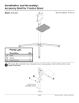
1
USER’S
MANUAL
PT-VME330B
16 - Port Synchronous Communications
Controller
PERFORMANCE
T ECHNOLOGIES, I NC
315 Science Parkway • Rochester, NY 14620
Tel: 716 256 0200 • Fax: 716 256 0791
Document Number 126A0256
PERFORMANCE
T ECHNOLOGIES, I NC
Rev
ECN
Pages Affected
Date
10
Initial Release
All
3/13/97
REVISION CONTROL
When reviewing this document please note any issues that you may have with the document (errors, points of confusion, grammar or spelling mistakes, etc.) and contact Technical Customer Support @ (716) 256-0248 or
[email protected]. All comments, suggestions, and criticisms are welcome.
Copyright Notice
© 1997 by Performance Technologies Inc. -- Printed in USA.
315 Science Parkway, Rochester, New York 14620
Trademark
PTbug is a trademark of Performance Computer.
All other brands or names are trademarks of their respective holders.
ii 16 - Port Synchronous Communications Controller User’s Manual
PERFORMANCE
T ECHNOLOGIES, I NC
NOTICE
This document presents information for users of the Performance Computer Model PT-VME330B 16 Port Synchronous Communications Controller.
Although the information contained within this document is considered accurate and characteristic of the
subject product, Performance Computer reserves the right to make changes to this document and any products described herein to improve reliability, function, or design. Performance Computer does not assume
any liability arising out of the application or use of any product or circuit described herein.
No part of this document may be copied or reproduced in any form or by any means without the prior
permission of Performance Computer.
WARNING
THIS EQUIPMENT GENERATES, USES, AND CAN RADIATE RADIO FREQUENCY ENERGY
AND, IF NOT INSTALLED AND USED IN ACCORDANCE WITH THE INSTRUCTION MANUAL,
MAY CAUSE INTERFERENCE TO RADIO COMMUNICATIONS. AS TEMPORARILY
PERMITTED BY REGULATION, IT HAS NOT BEEN TESTED FOR COMPLIANCE WITH THE
LIMITS FOR CLASS A COMPUTING DEVICES PURSUANT TO SUBPART J OF PART 15 OF FCC
RULES, WHICH ARE DESIGNED TO PROVIDE REASONABLE PROTECTION AGAINST SUCH
INTERFERENCE. OPERATION OF THIS EQUIPMENT IN A RESIDENTIAL AREA IS LIKELY TO
CAUSE INTERFERENCE, IN WHICH CASE THE USER, AT HIS OWN EXPENSE, WILL BE
REQUIRED TO TAKE WHATEVER MEASURES MAY BE REQUIRED TO CORRECT THE INTERFERENCE.
16 - Port Synchronous Communications Controller User’s Manual iii
PERFORMANCE
T ECHNOLOGIES, I NC
Safety Information
This section is provided as a summary of the safety recommendations throughout this manual. Performance Computer
(PCC) recommends that all safety precautions are followed to prevent harm to yourself or the equipment. Please follow
all warnings marked on the equipment.
Safety Precautions
• Follow all warnings and instructions marked on the equipment.
• Ensure that the voltage and frequency of your power source matches the voltage and frequency inscribed on the
equipments electrical rating label.
• Never push objects of any kind through the openings in the equipment. Dangerous voltages may be present. Conductive foreign objects could produce a short circuit that could cause fire, electrical shock, or damage your equipment.
Symbols
The following symbols appear in this document.
!
CAUTION: There is risk of personal injury or equipment damage. Follow the instructions.
WARNING: Hazardous voltages are present. To reduce the risk of electric shock and danger to personal
heath, follow the instructions.
iv 16 - Port Synchronous Communications Controller User’s Manual
PERFORMANCE
T ECHNOLOGIES, I NC
Table of Contents
Section 1 INTRODUCTION
Scope
Applicable Documents
Model Designations
1
1
2
2
Features
Additional Features Of The PT-VME330B
Code Portability Between PT-VME330A And PT-VME330B-Axx
Code Portability Between PT-VME330A-Axx And PT-VME330B
Code Portability Between PT-VME330A-Bxx And PT-VME330B-Bxx
Glossary and Conventions
3
4
4
4
5
6
6
7
Glossary
Conventions
Section 2 GETTING STARTED
Unpacking and Inspection
Hardware Configuration
9
9
9
Device Positions
10
Jumper Setup
Configuration
Software Configuration Options
Jumper Configuration Options
Socket U7 (formally U39 on PT-VME330A) Jumper Configuration
Socket U8 (formally U19 on PT-VME330A) Jumper Configuration
PROM/ROM/EEPROM/SRAM Socket Memory Map Options
Interrupt Priority Setting
Front Panel Reset and Abort Input Enable Jumpers
Factory Configurations
Board Installation
11
11
11
12
12
14
15
16
16
16
17
Power Considerations
Mechanical And Environmental
Slot Considerations
Backplane Insertion
Board Specifications
17
17
17
17
18
Break Out Box (BOB) Cabling
19
High Speed Synchronous Communications Controller User’s Manual i
Table of Contents
Serial Port Cabling
Example
Mechanical restraints
Debug Card and Cables
20
20
21
21
22
Section 3 FUNCTIONAL DESCRIPTION
Hardware Functions
Internal Architecture
Microprocessor
Main Memory
DRAM
Addressing
PROM Sockets
Serial EEPROM
Timers
Utility Serial Port
Communications Devices
Peripheral Device Dma Controller
I/O Interconnect
VMEbus Slave Interface
VMEbus Master Interface
Operating Controls And Indicators
“FAULT” Indicator
“I/O DMA” Indicator
“VME ACCESS” Indicator
External Reset And Abort
Section 4 FUNCTIONAL SUMMARY
Firmware - Hardware Interface
23
25
25
25
25
25
25
25
26
26
26
26
26
27
27
27
27
27
28
28
28
29
29
General Memory Map
Dynamic Memory Control
Utility Serial I/O
UART Control
Baud Rate Generation
Software Interrupt Time
29
35
35
35
35
36
Control/Status Registers
36
Serial EEPROM Operation
Control Register 0
Status Register
Processor Access To Serial Adapter Module
Register Access
Peripheral DMA Controller Operation
ii High Speed Synchronous Communications Controller User’s Manual
36
36
37
39
39
39
PERFORMANCE
T ECHNOLOGIES, I NC
MAR/TCR Memory Locations
DMA Terminal Count Interrupts
Peripheral DMA Command Register
VMEbus Mailboxes And Software Reset
Mailbox Slave Address Decoder
Configuring The Mailbox Interrupts
Software Reset
Enabling The VSI
VMEbus Interrupter
Poll the VMEbus Interrupt Request Level Register until status indicates “not busy”.
VMEbus Master Interface
Control Register 0
Control Register 1
VMEbus Cycle Timer
Section 5 APPENDICES
APPENDIX A: Product Warranty
APPENDIX B: Product Return Procedure and Form
APPENDIX C: Product Support
APPENDIX D: Installation Notes
APPENDIX E: EEPROM Usage
EEPROM Default Values
Section 6 INDEX
40
40
41
41
42
42
42
42
42
43
43
44
45
46
47
47
48
49
50
51
51
53
High Speed Synchronous Communications Controller User’s Manual iii
Table of Contents
iv High Speed Synchronous Communications Controller User’s Manual
PERFORMANCE
T ECHNOLOGIES, I NC
List of Figures
Figure 1: PT-VME330B Device Positions
Figure 2: U7 Setup Jumpers
Figure 3: PT-VME330B Front Panel
Figure 4: Example Serial port Cable
Figure 5: Block Diagram
10
12
19
21
24
High Speed Synchronous Communications Controller User’s Manual v
List of Figures
vi High Speed Synchronous Communications Controller User’s Manual
PERFORMANCE
T ECHNOLOGIES, I NC
List of Tables
Table 1: Automatic Programmable Configuration Process
Table 2: U7 Jumper Settings
Table 3: U8 Jumper Settings
Table 4: U7 and U8 Jumper Settings
Table 5: K15 Interrupt Jumper Settings
Table 6: Front Panel Reset18/Abort Jumper Settings
Table 7: K4, K16 & K17 Jumper Settings
11
13
14
15
16
16
16
High Speed Synchronous Communications Controller User’s Manual vii
List of Tables
viii High Speed Synchronous Communications Controller User’s Manual
Section
1
INTRODUCTION
Scope
This document provides information for users of the Model PT-VME330B High Speed Synchronous
Communications Controller.
This manual is not intended as a stand-alone document. If you plan on writing software for the board the
references cited below in the Applicable Documents section are necessary.
This manual does provide the information necessary to understand the operation and features of the
board. A prime objective was to answer those question raised by system developers as to whether the PTVME330B will complement their architecture. When the information in this document is combined with
the supporting documentation listed below, a complete description of PT-VME330B High Speed
Synchronous Communications Controller facilities is presented
Section 1 Provides an introduction and general overview of the PT-VME330B. It is intended as a quick
summary of PT-VME330B features and provides a framework for the rest of the document.
Section 2 (Getting Started) describes the physical setup and installation procedures.
Section 3 The Functional Description provides a detailed description of PT-VME330B architecture and
functional blocks.
Section 4 Summarizes the PT-VME330B memory map, registers, controls, indicators, etc.
Section 5 Review of Serial Adapter Module (SAM) functionality.
Section 6 (Connector Pinouts) summarizes the PT-VME330B external connections.
Section 7 Describes mechanical and environmental characteristics of the PT-VME330B.
Section 8 Appendices.
Section 9 Index.
Section 10 Schematics.
PT-VME-330B User’s Manual 1
Section
1
INTRODUCTION
Applicable Documents
a.
VMEbus Specification Manual, Revision C.1, ANSI/IEEE STD 1014-1987, VMEbus International
Trade Association (VITA). VITA; 10299 N. Scottsdale Road, Suite B; Scottsdale, AZ 82523.
b.
M68000 Family Programmer’s Reference Manual; M6800PM/AD. Motorola Incorporated, 1989.
Motorola Literature Distribution; P.O. Box 20912; Phoenix, AZ 85036.
c.
MC68EC030 32-Bit Embedded Controller User’s Manual; MC68EC030UM/AD. Motorola Incorporated, 1990. Motorola Literature Distribution; P.O. Box 20912; Phoenix, AZ 85036.
d.
MC68901 Multi-Function Peripheral; January, 1984. Motorola Semiconductor Products Incorporated; 3501 Ed Bluestein Boulevard; Austin, TX 78721.
e.
Z85230 Synchronous Communications Controller Manual; Technical Manual. Zilog, Inc.; 210
Hacienda Ave.; Campbell, CA 95008-6609.
f.
93C46 Data Sheet. Catalyst Semiconductor, Inc. or International CMOS Technology, Inc.
g.
Trooper, User Manual; 891006.MD300.01. Tundra Microsystems; 603 March Road; Kanata,
Ontario, Canada K2K 2M5.
Model Designations
The PT-VME330B is a modular design which may be equipped with a variety of Serial Adapter Module
(SAM) interface units and physical interface or Break Out Box (BOB) options. The PT-VME330B only
comes in a 6U version, but a 9U adapter module can be purchased for any 9U factor requirements.
6U VMEbus models are available with either 4MByte or 8Mbytes of memory and with a number of SAM
interface options. Model numbers are formed as follows:
Model PT-VME330B-10726
Model PT-VME330B-10727
4 Megabyte of DRAM serial I/O controller mother board
8 Megabyte of DRAM serial I/O controller mother board
The required SAM Modules (one SAM only, per VME330B) model designations are as follows:
Model PT-SAMR-10728
Model PT-SAMS-10729
Model PT-SAMT-10730
16 Port RS-232 Adapter
8 Port RS-232 Adapter
16 Port RS-422 Adapter
The PT-VME330B Hardware Options/Accessories model designations are as follows:
Model PT-ACC1xx-10247
Model PT-ACC330-AAB
Console Debug Card and Cables for PT-VME330A/B
6’ Unterminated Cable for PT-VME330A/B
The PT-VME330B Break Out Box Hardware Options/Accessories model designations are as
follows:
Model PT-ACC330-BAA
Model PT-ACC330-BCA
Model PT-ACC330-CAA
2 PT-VME-330B User’s Manual
Floor unit, 8 Port Breakout w/cables for RS-232
Rack unit, 8 Port Breakout w/cables for RS-232
Floor unit, 8 Port Breakout w/cables for RS-449
PERFORMANCE
T ECHNOLOGIES, I NC
Model PT-ACC330-CCA
Model PT-ACC330-EAA
Model PT-ACC330-ECA
Rack unit, 8 Port Breakout w/cables for RS-449
Floor unit, 16 Port Breakout w/cables for RS-232
Floor unit, 16 Port Breakout w/cables for RS-232
Features
• 68EC030 MPU Running At 32 MHz
Four Or Eight MByte One-Wait-State Dynamic Memory For Code And Data
Two 32-Pin JEDEC PROM Sockets For Software Boot
PTI Proprietary VMEbus Slave Interface ASIC (VSI)
16 Byte Dual-Ported Mailbox With Programmable Slave Address
Programmable Interrupt Of On-Board MPU Upon VMEbus Access Of Mailboxes
Internal EEPROM For Storage Of Setup Parameters
Up To 16 Communications Ports Using Eight Z85230 Devices.
32 Channel DMA Controller (Transmit And Receive On 16 Ports).
Aggregate DMA Bandwidth of 4.0 Mbits/Second yields 125 Kbits/second full duplex bandwidth
on all 16 ports or correspondingly higher bandwidth on fewer ports and/or channels.
Flexible DMA Control Allows Unrestricted Use Of Internal Buffer (1MByte MAR And TCR Per
Channel).
• VMEbus Interrupter With Programmable Request Level and Vector
PTI Proprietary VMEbus Slave Interface ASIC (VSI)
16 Byte Dual-Ported Mailbox With Programmable Slave Address
VMEbus Software Initiated Reset Function.
VMEbus Master Interface.
A32:D32 With Block Mode.
Software Programmable Request Mode And Level.
• Two Programmable Utility Timers.
• RS-232 Utility Port.
• Front Panel User Interface Features
Front Panel I/O Connection To Passive “Break Out” Panel
• Signal Distribution
Passive Cabling Scheme
Front Panel or “P2” Cable Access
• Mechanical
Single Slot Utilization
• Software Support
PTbug Debugger/Monitor
UconX Software
PT-VME-330B User’s Manual 3
Section
1
INTRODUCTION
Additional Features Of The PT-VME330B
Comparing the features of the PT-VME330B versus the PT-VME330A, the PT-VME330B has:
• A 32 MHz MC68EC030 processor versus 16 MHz MC68020.
• The capability of 4 or 8 Mbytes of memory versus 1 or 4 Mbyte.
• Expanded JEDEC PROM sockets supporting up to 8Mbit devices.
• Jumper selectable Interrupt Priorities.
• Jumper Enable/Disable of serial port Reset and Abort inputs.
Code Portability Between PT-VME330A And PT-VME330B-Axx
Code developed for the PT-VME330A-Bxx (4 Mbyte) will operate on the PT-VME330B-Axx (4 Mbyte)
with little or no modification. If code ported from a PT-VME330A does not operate correctly, the
following areas should be checked:
• The increased processor speed will upset any processor-speed-based delays.
• Jedec PROM socket jumper settings.
• Interrupt Priority encoding Jumper.
• 68EC030 Processor Data Cache.
Code Portability Between PT-VME330A-Axx And PT-VME330B
Code developed for the PT-VME330A-Axx (1 Mbyte) will need a minor modification to operate
correctly on the PT-VME330B-Axx (4 Mbyte) or PT-VME330B-Bxx (8 Mbyte). The Peripheral DMA
Controller MAR and TCR locations are located relative to the end of memory rather than at an absolute
address. Thus the MAR/TCR locations are at different absolute addresses for the 1 Mbyte, 4 Mbyte and
8 Mbyte versions of the module.
4 PT-VME-330B User’s Manual
PERFORMANCE
T ECHNOLOGIES, I NC
Code Portability Between PT-VME330A-Bxx And PT-VME330BBxx
Code developed for the PT-VME330A-Bxx (4 Mbyte) will need a minor modification to operate
correctly on the PT-VME330B-Bxx (8 Mbyte). The Peripheral DMA Controller MAR and TCR locations are located relative to the end of memory rather than at an absolute address. Thus the MAR/TCR
locations are at different absolute addresses for the 4 Mbyte and 8 Mbyte versions of the module.
PT-VME-330B User’s Manual 5
Section
1
INTRODUCTION
Glossary and Conventions
Glossary
DIP - Dual In-line Package. Standard, ‘through-hole’ integrated circuit package.
DRAM - Dynamic Random Access Memory
EEPROM - Electrically Erasable Programmable Read Only Memory
EPROM - Erasable Programmable Read Only Memory
longword - In this manual, this term indicates a 32-bit value.
MByte - Mega Byte.
ms. - Millisecond.
PAL - Programmable Array Logic.
reserved - The term used for bits, bytes, fields, code values, etc. that are set aside for future use.
RTC - Real Time Clock
SRAM - Static Random Access Memory.
word - In this manual, this term indicates a 16-bit value.
xxh - Numbers followed by lowercase h are hexadecimal values. All other numbers are decimal values.
6 PT-VME-330B User’s Manual
PERFORMANCE
T ECHNOLOGIES, I NC
Conventions
Upper case names enclosed in square brackets ([,]) represent signal names that can be found in the schematics.
Numbers enclosed in “less than” (<) and “greater than” (>) symbols refer to individual bits of a signal
bus. i.e. +MPA<0> represents a the least significant bit of the 32 bit MicroProcessor Address bus.
+MPA<0:31> represents all signals associated with the MicroProcessor Address bus.
Device pins are referenced with a Reference Designator, hyphen, pin number. i.e. U52-30 indicates pin
30 of location U52.
VMEbus signal pins are referenced with the Connector Designator, hyphen, Row Designator, Pin
number. i.e. P2-B3 refers to Pin 3 of Row B on the VMEbus “P2” connector.
PT-VME-330B User’s Manual 7
Section
1
INTRODUCTION
8 PT-VME-330B User’s Manual
Section
2
GETTING STARTED
Unpacking and Inspection
!
CAUTION: ELECTRONIC COMPONENTS ON MODERN PRINTED CIRCUIT BOARDS ARE
EXTREMELY SENSITIVE TO STATIC ELECTRICITY. ORDINARY AMOUNTS OF STATIC
ELECTRICITY GENERATED BY YOUR CLOTHING OR WORK ENVIRONMENT CAN
DAMAGE THE ELECTRONIC EQUIPMENT. IT IS RECOMMENDED THAT WHEN
INSTALLING THE PT-VME330B IN A SYSTEM OR THE COMPONENTS ON THE BOARD
ITSELF THAT ANTI-STATIC GROUNDING STRAPS AND ANTI-STATIC MATS ARE USED TO
HELP PREVENT DAMAGE DUE TO ELECTROSTATIC DISCHARGE.
The shipping carton should be inspected for any possible damage that may have occurred during shipment. If there is any physical damage to the package you have opened, immediately contact the Shipping
Carrier and/or Performance Technologies, Incorporated.
If this shipment is being received outside the United States or Canada and there is damage to the package,
contact your local distributor or agent.
If there is shipping damage, failure to make an immediate claim may void any insurance coverage.
If no external damage is visible, carefully unpack contents from shipping carton, observing anti-static
precautions identified above and verify against packing list. Inspect the PT-VME330B for any visible
signs of shipping damage. If such physical damage is noted, report it immediately to Performance Technologies or appropriate agent. DO NOT PROCEED with any further configuration or installation.
!
NOTE: If any damage is detected follow the Product Return Procedure described in the appendix.
If no damage is visible, check that all socketed parts are firmly seated. Occasionally parts work themselves loose or partially out of their sockets during the shipping process. Reseat any loose devices by
placing the printed circuit board on a flat surface and pressing firmly down on the part. If a part has
worked itself completely free of the board (a highly unlikely event) be sure to verify its position and
orientation before reinsertion. Check that all mounting screws of attached assemblies are tight.
The serial number can be found stamped on the solder side of the PCB along the edge closest to the front
panel. A printed label identifying the assembly revision level can be found on the component side of the
“P1” connector. See “PT-VME330B Device Positions” on page 10.
Hardware Configuration
A layout for the PT-VME330B is shown in “Figure 1: PT-VME330B Device Positions”. There are
various jumpers to configure user options which must be set before initial bootup. Refer to the information in this section to verify that you have the correct settings.
PT-VME-330B User’s Manual 9
Section
2
GETTING STARTED
Device Positions
U7
U8
Caution:
Note Orientation
Caution:
Note Orientation
Serial
No.
Assy
Rev
Label
K11
K7,8 & 10
Switch SW1
K1 - K6
PORT A
K9
PORT B
K17
K12 -16 & 18
RS-232
CONSOLE
PORT
Figure 1: PT-VME330B Device Positions
10 PT-VME-330B User’s Manual
PERFORMANCE
T ECHNOLOGIES, I NC
Jumper Setup
Configuration
Configuration of the PT-VME330B takes place on two levels:
Software Programmable Configuration Options - the configuration options normally associated with
jumpers or switches, such as Slave Address, Bus Request Level and Mode, and Interrupt Request Level,
are software/firmware controllable on the PT-VME330B.
Jumper Configuration Options - This group is generally set by PTI at the factory; either to a factory
default or to customer requirements. Generally, these options should not require field alteration, but
should alteration be necessary, full configuration information is provided.
Software Configuration Options
The programmable configuration capability of the PT-VME330B presents a number of opportunities not
available in a jumper or switch configured board. To users accustomed to “hard” configured modules,
the capability also presents some challenges.
One application which illustrates the power of software configuration is a system with multiple PTVME330Bs. A traditional “hard” configuration would require that each module be configured per a chart
or table of addresses, and the possibility of mistakes, particularly in a field service situation, is very real.
Combining the programmable configuration capability of the PT-VME330B with a relatively simple
power-up address assignment program would allow the system to automatically configure the PTVME330Bs in the system according to their relative positions in the card cage. Such a program relies on
the attributes of the VMEbus “IACK” daisy chain to determine the relative positions of each module. A
simplified logical flow for an example auto assignment program is shown below. The program is
designed to assign “sequence numbers” to an arbitrary number of PT-VME330Bs based on their relative
position in the card cage, the module physically nearest slot one being assigned “sequence one”. The
program requires that the slot one module “know” that it is in slot one - all other modules run exactly the
same program. The “--->” symbol indicates a direct causal relationship.
Table 1: Automatic Programmable Configuration Process
Slot 1
Module Activity
Relation
ship
Slot 2-N
Module(s) Activity
1
Complete power-up tests,
interrupt priority high
N/A
All modules complete powerup tests, VSI disabled.
2
Delay
N/A
Slot 2-N modules issue VMEbus interrupt
3
Lower priority to allow slot
2 module to interrupt
--->
Slot 2 module gets IACK, VSI
enabled at temporary address
Step
PT-VME-330B User’s Manual 11
Section
2
GETTING STARTED
Table 1: Automatic Programmable Configuration Process
Slot 1
Module Activity
Relation
ship
Slot 2-N
Module(s) Activity
4
Write 1st sequence number
to slot 2 module VSI at temporary address
--->
Slot 2 module changes address
of VSI from temporary to final
as determined by sequence
number
5
Lower priority to allow slot
N module to interrupt
--->
Slot N module gets IACK, VSI
enabled at temporary address
6
Write Nth sequence number
to slot N module VSI at
temporary address
--->
Nth module changes address of
VSI from temporary to final as
determined by sequence number
7
Repeat 5-6 until no more
additional interrupt
requests are pending
N/A
All modules are at their final
addresses as determined by
sequence number
Step
Jumper Configuration Options
These options are typically installed by PTI at the factory to customer requirements. Using the information in the following paragraphs, however, they may be altered by the customer
All Jumper Blocks on the System Board are designed to mate with standard 2 pin jumper shunts. Spare
jumper shunts can be stored by slipping one side of the jumper shunt on a single, unused pin of a jumper
block and allowing the other side of the jumper shunt to hang in space. As shown at left:
Socket U7 (formally U39 on PT-VME330A) Jumper Configuration
Figure 2: U7 Setup Jumpers
K1- K2
K11
K10
12 PT-VME-330B User’s Manual
The pin out configuration for location U7 is defined by Jumpers K1,2,11
and K10 (highlighted at left). Each jumper consists of a column of three
adjacent pins.
When installing a 28 pin device be sure that pin 14 of the device enters pin
16 of the socket (bottom justified).
PERFORMANCE
T ECHNOLOGIES, I NC
The jumpers at locations K1, K2, K10 and K11 allow for variations in the pinout of PROM/ROM socket
U7 according to the following table. When installing 28 pin devices, be sure that pin 14 of the device
enters pin 16 of the socket (bottom justified). The bolded text indicates the factory configuration.
Table 2: U7 Jumper Settings
PROM/ROM
Type
Jumpers
Installed
32Kx8 28pin
K1-2 to K1-3
K2-2 to K2-3
K10-2 to K10-3
K11-2 to K11-3
64Kx8 28pin
K1-2 to K1-3
K2-1 to K2-2
K10-2 to K10-3
K11-2 to K11-3
128Kx8 32pin
K1-2 to K1-3
K2-1 to K2-2
K10-2 to K10-3
K11-2 to K11-3
256Kx8 32pin
K1-1 to K1-2
K2-1 to K2-2
K10-2 to K10-3
K11-2 to K11-3
512Kx8 32pin
K1-1 to K1-2
K2-1 to K2-2
K10-1 to K10-2
K11-2 to K11-3
1024Kx8
32pin
K1-1 to K1-2
K2-1 to K2-2
K10-1 to K10-2
K11-1 to K11-2
!
CAUTION: WHEN INSERTING 28 OR 32 PIN DEVICES INTO LOCATIONS U7 OR U8 NOTE THE
ORIENTATION OF THE CHIP! THE BOTTOM OF THE CHIP WILL BE ALIGNED WITH THE
BOTTOM OF THE SOCKET.
!
CAUTION: THE DEVICE MUST HAVE AN ACCESS TIME OF LESS THAN OR EQUAL TO
200 NS.
PT-VME-330B User’s Manual 13
Section
2
GETTING STARTED
Socket U8 (formally U19 on PT-VME330A) Jumper Configuration
K5- K6
K9
K7 - K8
The jumpers at locations K5-K9 allow for variation in the pinout of socket
U8 according to the following table. When installing a 28 pin device be
sure that pin 14 of the device enters pin 16 of the socket (bottom justified).
EEPROMs used in this application must have write protection built in. The
bolded text indicates the factory configuration.
Table 3: U8 Jumper Settings
PROM/ROM
Type
14 PT-VME-330B User’s Manual
Jumpers Installed
Example AMD
Part Numbers
64Kx8 28pin
K5-1 to K5-2
K6-2 to K6-3
K7-2 to K7-3
K8-2 to K8-3
K9-2 to K9-3
AM27C512-150DC
AM27C512-120DC
128Kx8 32pin
K5-1 to K5-2
K6-2 to K6-3
K7-2 to K7-3
K8-2 to K8-3
K9-2 to K9-3
AM27CD10-150DC
AM27CD10-120DC
256Kx8 32pin
K5-1 to K5-2
K6-2 to K6-3
K7-1 to K7-2
K8-2 to K8-3
K9-2 to K9-3
AM27C020-150DC
AM27C020-120DC
512Kx8 32pin
K5-1 to K5-2
K6-2 to K6-3
K7-1 to K7-2
K8-1 to K8-2
K9-2 to K9-3
AM27C040-150DC
AM27C040-120DC
1024Kx8
32pin
K5-1 to K5-2
K6-2 to K6-3
K7-1 to K7-2
K8-1 to K8-2
K9-1 to K9-2
Non-AMD Parts
AT27C080-12PC
SGSM27C801-100
8Kx8 28pin
EEPROM/
SRAM
K6-1 to K6-2
K7-2 to K7-3
32Kx8 28pin
EEPROM/
SRAM
K5-2 to K5-3
K6-1 to K6-2
K7-2 to K7-3
PERFORMANCE
T ECHNOLOGIES, I NC
!
CAUTION: WHEN INSERTING 28 OR 32 PIN DEVICES INTO LOCATIONS U7 OR U8 NOTE THE
ORIENTATION OF THE CHIP! THE BOTTOM OF THE CHIP WILL BE ALIGNED WITH THE
BOTTOM OF THE SOCKET.
!
CAUTION: THE DEVICE MUST HAVE AN ACCESS TIME OF LESS THAN OR EQUAL TO
200 NS.
PROM/ROM/EEPROM/SRAM Socket Memory Map Options
The jumpers at locations K3 and K18 allow for setting the read/write permissions of devices inserted into
sockets U7 and U8 according to the following table. EEPROMs used in this application must have write
protection built in. The bolded text indicates the factory configuration.
1
K18
K3
.
Table 4: U7 and U8 Jumper Settings
Option
Device Type
Jumpers Setting
1
00000000-0001FFFF Read-Only Memory Socket, U7
K3-1 to K3-2
00020000-0003FFFF Read/Write Memory Socket. U8
K18 OPENa
00000000-0003FFFF Read-Only Memory Socket, U7
K3-2 to K3-3
00040000-0007FFFF Read/Write Memory Socket. U8
K18 OPENa
00000000-0007FFFF Read-Only Memory Socket, U7
K18-1 to K18-2
00080000-000FFFFF Read/Write Memory Socket. U8
K3 OPENa
00000000-000FFFFF Read-Only Memory Socket, U7
K18-2 to K18-3
00100000-001FFFFF Read/Write Memory Socket. U8
K3 OPENa
2
3
4
a. NOTE: Never install jumpers on both K3 and K18 at any time!
!
CAUTION: Before enabling this function be sure that your installed software supports it. Unexpected
local resets could occur.
1
PT-VME-330B User’s Manual 15
Section
2
GETTING STARTED
Interrupt Priority Setting
Jumper K15 selects between two available Interrupt maps. The bolded text indicates the factory configuration.
Table 5: K15 Interrupt Jumper Settings
Option
Jumpers Setting
1
K15-2 to K15-3
2
K15-1 to K15-2
See “Table 12: General Interrupt Map” on page 34.
Front Panel Reset and Abort Input Enable Jumpers
Jumpers K12, K13 and K14 allows you to select the following options for the optional front panel debug
cable. The bolded text indicates the factory configuration.
Table 6: Front Panel Reset18/Abort Jumper Settings
Option
Jumpers Setting
Reset Disabled
K12-2 to K12-3
Reset Enabled
K12-1 to K12-2
Abort NC (Normally Closed) Disabled
K13-1 to K13-2
Abort NC (Normally Closed) Enabled
K13-2 to K13-3
Abort NO (Normally Open) Disabled
K14-1 to K14-2
Abort NO (Normally Open) Enabled
K14-2 to K14-3
Factory Configurations
Jumper headers K4, K16 and K17 are for factory configuration and should not be altered by the user.
Table 7: K4, K16 & K17 Jumper Settings
Option
Jumpers Setting
Factory Setting
K4-1 to K4-2
Factory Set. Depends on the SAM board being
used
K16
4MB Base Board
K17-2 to K17-3
8MB Base Board
K17-1 to K17-2
16 PT-VME-330B User’s Manual
PERFORMANCE
T ECHNOLOGIES, I NC
Board Installation
Power Considerations
PT-VME330B VMEbus Controller has the following power requirements:
• +5V +/- 5% 5.0 Amps typical
• 6.0 Amps maximum
• +12V +/-5% .15 Amp maximum
• -12V +/-5% .15 Amp maximum
It is recommended that Maximum values are used to ensure adequate margins. Add these numbers to
those of the other devices in the system and check that the incorporation of the PT-VME330B does not
exceed the system power supply ratings.
Mechanical And Environmental
Ambient Temperature:
• 0o to +55o C, operating
• -55o to +85o C, storage
Humidity:
• 0% to 90% (non-condensing)
Physical
• Width: 234mm (9.2in)
• Depth: 160mm (6.3in)
• Front Panel: 20.3mm (0.8in)
Slot Considerations
The programmable configuration capability of the PT-VME330B presents a number of opportunities not
available in a jumper or switch configured board. To users accustomed to “hard” configured modules,
the capability also presents some challenges. See “Software Configuration Options” on page 11 for more
information.
Backplane Insertion
!
CAUTION: The chassis must be switched off before inserting the board or making any cable connections
to avoid damage to the components!
PT-VME-330B User’s Manual 17
Section
2
GETTING STARTED
After reviewing the Power Considerations and selecting a slot, insert the PT-VME330B into the backplane. Be sure that it is seated completely into the backplane then tighten the two Captive Chassis
Mounting Screws on the front panel. Attach cables as necessary then power up the system.
!
NOTE: The first time the system is powered up after inserting the card, check the supply voltages at the
PT-VME330B backplane P1 and P2 connectors. Adjust the supplies as necessary to the nominal voltage
levels (+12.00V, - 12.00V and +5.00V).
Board Specifications
Characteristic
Specification
Processor
68EC030 @ 32 MHz.
Main RAM
4 or 8 MByte Dynamic
1 wait state @ 32 MHz
PROM/EEPROM/SRAM
2 32-pin JEDEC Byte Ports
Socket 1:
32Kx8 PROM or
64Kx8 PROM or
128Kx8 PROM or
256Kx8 PROM or
512Kx8 PROM or
1024Kx8 PROM
Socket 2
64Kx8 PROM or
128Kx8 PROM or
256Kx8 PROM or
512Kx8 PROM or
1024Kx8 PROM or
8Kx8 EEPROM or
8Kx8 SRAM or
32Kx8 EEPROM or
32Kx8 SRAM
VMEbus Master
A32/A24: D32/D16
Block Mode
Unaligned Transfers
VMEbus Slave
A32/A24/A16 D8(O)
Peripheral DMA
1 Port at 1778 Kbps each Port
Controller
2 Ports at 1000 Kbps each Port
Full Duplex
4 Ports at 526 Kbps each Port
Performance
8 Ports at 271 Kbps each Port
16 Ports at 137 Kbps each Port
18 PT-VME-330B User’s Manual
PERFORMANCE
T ECHNOLOGIES, I NC
Figure 3: PT-VME330B Front Panel
Captive Chassis Mount Screw
PT-VME
330B
Ejector Handle
FAULT
System Status Indicators
I/O DMA
VMEBUS
Port A
Port B
RS-232 Utility Port
PERFORMANCE
T ECHNOLOGIES, I NC
Ejector Handle
Captive Chassis Mount Screw
Break Out Box (BOB) Cabling
The PT-VME330B uses an range of optional breakout boxes supplied with industry standard connectors.
The breakout box kit includes the termination box with appropriate connectors and 6 foot terminated
cables (cut to user specified lengths, on special order). The boxes are available in 19 inch rack mount
versions only.
PT-VME-330B User’s Manual 19
Section
2
GETTING STARTED
Serial Port Cabling
14
12
10
8
6
4
2
13
11
9
7
5
3
1
PERFORMANCE
T ECHNOLOGIES, I NC
The PT-VME330B Utility Serial Port interconnect is provided on the front panel. The signals are organized so that a mass terminated Insulation Displacement Connectors (IDC) can be used to create an RS232 DTE interconnect. A 12 inch transition cable is supplied with the PT-VME330B which converts
between the 14-pin header and a female shell (male pin) 25-pin D-Shell connector. If a longer cable or a
different D-Shell connector sex is required it can be assembled by following the example below. The
Utility Port pin positions are noted in the figure to the left.
NOTE: The EIA RS232C Specification limits the maximum end to end cable length to 50 ft.
Example
Following is an example cable with vendors and part numbers for the components. These configurations
have been tested at PTI. Figure 4 displays an example serial cable for the PT-VME330B. The view is
with the connector sockets pointing towards you.
An interface cable can be constructed using a 14 conductor ribbon cable to attach a 25-Pin D-Shell IDC
to a 14 contact ribbon cable IDC socket. To conserve front panel space only a 14 pin connector is used,
however the 25-Pin D-Shell expects 25 conductors, so pin-1 of the ribbon cable must be justified to the
pin-1 end of the D-Shell connector. It is recommended that the cable be no longer than necessary for your
particular application.
D-Shell Connection
25 position Insulation Displacement Connector Male, D-Shell connector derived from DIN 41612
type C, with rows A and C populated (socket):
3M 8225-6003 or
T&B 609-25P-MA2
Ribbon cable
14 Conductor 28 AWG. Flat Cable
Spectra-Strip 843-191-2801-014 or
3M 3365/14
RS232 Serial Port connector
14 Pin Flat Cable Connector center polarized
Burndy FRS14BF-8 (strain relief included) or
AMP 746288-2 (connector)
AMP 499252-9 (strain relief)
20 PT-VME-330B User’s Manual
PERFORMANCE
T ECHNOLOGIES, I NC
Figure 4: Example Serial port Cable
50 Foot Maximum
Pin 1 Indicator
1
1
14 Conductor Ribbon Cable
14 Pin Flat Cable Connector
25 Pin D-Shell Connector
Mechanical restraints
Depending upon your mechanical configuration, tie wraps or cable clamps may be necessary to provide
mechanical support for the cable.
Debug Card and Cables
The PT-ACC1xx-10247 Kit contains a 9 inch cable and a PCB board that has Abort and Reset buttons
to be used during software development.
NOTE: The EIA RS232C Specification limits the maximum end to end cable length to 50 ft.
PT-VME-330B User’s Manual 21
Section
2
GETTING STARTED
22 PT-VME-330B User’s Manual
Section
3
FUNCTIONAL DESCRIPTION
The Performance Technologies PT-VME330B 16 Port Serial I/O VMEbus Controllers a high performance synchronous communications controller which offers excellent performance, powerful functional
features, and high ports-per-slot density.
The PT-VME330B is designed specifically for synchronous communication requirements that demand
high throughput and/or maximum ports/module capacity. The module’s communication interface is
based on up to eight Z85230 Synchronous Communication Controllers (SCC’s) supporting a variety of
physical line interfaces.
Designed as a fully programmable communications sub-system, it is capable of sustaining high data rates
for a variety of protocols used in synchronous and asynchronous data communications.
Unlike other controllers, the onboard intelligences and large DRAM array of the PT-VME330B allow it
to handle much of the low level communications activities that typically would burden the host. This can
greatly enhance overall system performance. The DRAM also allows the downloading of protocols for
stand-alone code execution directly on the PT-VME330B.
Operating under real world protocol overheads, this communications adapter can sustain the concurrent
throughput of over 137 Kbps full-duplex on each of its 16 channels and over 1.8 Mbits/sec using a single
channel.
The architecture of the PT-VME330B capitalizes on the intelligence of the Motorola MC68EC030 @ 32
MHz and up to eight dual channel Z85230 SCC’s. The 32 channel DMA controller is highly optimized
to ensure high speed data movement between the SCCs and the DRAM data buffer.
The high bandwidth local memory of the PT-VME330B provides the deterministic element necessary to
allow both SIO Transmit and Receive operations to continue on all ports without loss of data, even during
sustained and prolonged VMEbus accesses.
The PT-VME330B includes support for addressing 4 GBytes of memory and 32 bit data transfers. The
VMEbus interface also supports Block Mode (BLT) operation. This is especially effective for moving
large contiguous blocks of information while minimizing bus control overhead.
Physically, the PT-VME330B consists of a Base Board, a mezzanine mounted Serial Adapter Module
(S-A-M), and one or more passive Breakout Boards (B-O-B). The Controller contains the 68EC030,
memory, VMEbus interfaces, and DMA controller. The Serial Adapter contains the communications and
line interface devices. The Breakout Board provides the transition to the connector interface required.
PT-VME-330B User’s Manual 23
Section
3
FUNCTIONAL DESCRIPTION
Figure 5: Block Diagram
RS-232C
Console
Port
VMEbus
VME
Master Interface
PROM
EEPROM
SRAM
68901
2 * 32-pin Sockets
(optional)
VME Slave
Mailboxes
& VME Local
Interrupts
PT-VSI
Buffer
32 MHz
MC68EC030
32 Bit Data/Address
4 or 8 MB
Dual Ported
DRAM
1 wait state
32 Bit Data/Address
SCC Interrupts
32 Channel
DMA
Buffer
8 Bit Data/Address
Control
BOB Cable
Serial Adapter Module (SAM)
8 to 16 Ports
Break
Out
Box
(BOB)
24 PT-VME-330B User’s Manual
Line Interface
Z85230
Line Interface
Z85230
4 to 8 Z85230 & Line Interface Pairs
Line Interface
Z85230
Line Interface
Z85230
PERFORMANCE
T ECHNOLOGIES, I NC
Hardware Functions
Internal Architecture
The PT-VME330B VMEbus Controller is a dual internal bus design which allows accesses to VMEbus,
which are of indeterminate length, to take place without compromising the ability of the Peripheral DMA
Controller to transfer data.
All of the VMEbus setup parameters usually associated with jumper or switches are software programmable on the PT-VME330B. VMEbus slave address, master request level, and master request mode are
all programmable by the local processor. An EEPROM is provided for non-volatile storage of these
parameters. For those applications which demand a manual input, a four bit switch, accessible to the firmware, is provided.
Microprocessor
The PT-VME330B utilizes a Motorola 68EC030 Microprocessor running at 32 MHz.This processor
combines a full 32-bit Central Processing Unit (CPU) core, a data cache, an instruction cache, and an
enhanced bus controller in a single VLSI device.
Main Memory
Main memory is implemented using two or four 1M x 16 DRAMs.
DRAM
Main memory uses 60 ns. Fast Page Mode DRAMs, composed of a single bank of 16 MBit, 16 bit wide
devices. Thus, the board may be populated at the time of manufacture with 4 or 8 megabytes of RAM.
All of main memory can be mapped to the VMEbus.
Addressing
The address space from 40000000h to 4FFFFFFFh is allocated to the DRAM. Any reference to this 128
MByte space will complete without a bus error. Both the 4 and 8 MB base boards memory space will
repeat every 8 MB, thus there will be a 4 MB dead band of memory addresses between valid memory
address. (40000000h, 40800000h to 41000000h )
PROM Sockets
The board is equipped with two 32-pin JEDEC sockets configured as byte wide ports. Both sockets
support ROM, PROM, EPROM and EEPROM read-only devices, as well as 28-pin or 32-pin configuration Jumpers are provided to select between read-only and read/write operation and the 28-pin or 32-pin
configurations. See “ Jumper Configuration Options” on page 12.
Serial EEPROM
The EEPROM supports 128 bytes of non volatile memory. The part is capable of 10,000 erase/write
cycles and ten year data retention. Performance Technologies normally uses this memory to store various
parameters and options used in the initialization and operation of the PT-VME330B.
PT-VME-330B User’s Manual 25
Section
3
FUNCTIONAL DESCRIPTION
This device (U19) is socketed so that it can be moved to another board if necessary. For instance, if board
level replacement is typically performed on failures in the field. The EEPROM can be moved to the
replacement board to maintain the configuration information of the original board.
Timers
The 68901 Multi-Function Peripheral provides four timers. The timers are allocated as follows:
• Software Timer A
• VMEbus Time-out Timer
• Software Timer C
• Utility Port Baud Rate Generation
• The timers are driven by a 3.68 MHz timebase.
Utility Serial Port
This function is also provided by the 68901 MFP. The utility port is equipped with an RS-232 interface
and supports Transmit and Receive signals over the common asynchronous speed range.
The Utility Port connector is located on the front panel and uses a 14-pin dual row header connector.
Communications Devices
The VMEbus controller supports up to eight Z85230 Serial Communications Controllers operating at
14.7 MHz.
Peripheral Device Dma Controller
The Z85230 devices are served by a 32 channel DMA controller. This controller is configured so that one
channel is allocated to transmit and a separate channel is allocated to receive for each communications
port.
The controller stores a Memory Address Register value and a Transfer Count value, for each channel, in
a dedicated 64 longword field of on-board main memory.
During operation, a high-speed state machine receives the DMA request and fetches the MAR and TCR
values from memory. The MAR and TCR are incremented/decremented and replaced in memory. The
byte read or write cycle, at the address specified by the MAR, is then conducted and the data transferred
to/from the Z85230.
The DMA controller can interrupt the local processor on terminal count for both transmit and receive
operations. The interrupt vector will be derived from the DMA channel reaching terminal count - thus
each DMA channel will have a separate interrupt vector. DMA terminal count interrupts may be disabled
for receive channels only.
26 PT-VME-330B User’s Manual
PERFORMANCE
T ECHNOLOGIES, I NC
I/O Interconnect
All drivers and receivers are located on the Serial Adapter Module. Two 80 conductor ribbon cables
connect the Serial Adapter Module to the Breakout Board. The Breakout Board is completely passive
and serves to mount connectors only.
VMEbus Slave Interface
The VMEbus slave interface is implemented using the “VMEbus Slave Interface” ASIC (VSI).
The VSI has 16 byte-wide mailboxes accessible from both the VMEbus and the local processor bus. The
mailboxes monitor accesses from VMEbus and have the capability of interrupting the local processor
when VMEbus accesses are made. A flexible system of controls allows this monitor/interrupt function
to be adapted to specific firmware requirements.
The VSI also provides the VMEbus interrupter function. This interrupter is fully programmable - both
request level and vector number can be firmware selected.
The Host may issue a hardware reset of the PT-VME330B by accessing a specific location decoded by
the VSI. The location must be accessed using a specific data pattern to reduce the chances of inadvertent
reset.
VMEbus Master Interface
The PT-VME330B allows the local processor to have direct access to the VMEbus through the VMEbus
Master Interface.
VMEbus access appears as a portion of the local processor memory map and can be freely read or written
using full A32:D32 capability. During VMEbus accesses, AM0-5 and A31 are supplied from a local
register. All byte position translations and unaligned transfers are automatically performed.
The VMEbus request level and request mode (Release-When-Done or Release-On-Request) are software
programmable.
Because VMEbus accesses may be of indeterminate length (due to bus contention from unknown
sources), the PT-VME330B provides a level of logical isolation between the local memory array and the
VMEbus master interface. This isolation insures that the real-time requirements of the Z85230 DMA
Controller are not jeopardized by long processor accesses to VMEbus.
Operating Controls And Indicators
“FAULT” Indicator
The PT-VME330B “FAULT” indicator is a red LED under software control.
“I/O DMA” Indicator
The “I/O DMA” Indicator is illuminated whenever the Peripheral DMA controller has control of the
internal bus. The LED illumination intensity is a relative indication of the DMA activity.
PT-VME-330B User’s Manual 27
Section
3
FUNCTIONAL DESCRIPTION
“VME ACCESS” Indicator
The “VME Access” Indicator is illuminated whenever the PT-VME330B is accessing the VMEbus.
External Reset And Abort
The PT-VME330B has provision for external manual reset and abort (level 7 interrupt) switches. These
input lines are provided on the 14-pin Debug Port connector, are internally de-bounced, and require a
Form A (normally open) contact closure for Reset and a Form C (SPDT) contact for Abort.
28 PT-VME-330B User’s Manual
Section
4
FUNCTIONAL SUMMARY
Firmware - Hardware Interface
This section provides a functional reference of address, interrupt, and bit assignments.
When a function is implemented using commercially available VLSI, the device register names are given
along with any special programming requirement. This information should be used in conjunction with
the manufacturers data sheet for more detail as to specific bit fields, etc.
When a function is implemented using hardware unique to the PT-VME330B, the register bit definitions
are included in that section. Note that some PT-VME330B registers may have application in more than
one functional area - in this case the register diagram is repeated but only those bits applicable to the function are described.
General Memory Map
The memory map for the 4 MByte and 8 Mbyte versions is identical except for the end of the DRAM
range and the location of the Peripheral DMA Controller MARs and TCRs.
Table 8: General Memory Map
OPTION
MEMORY RANGE
(HEX)
DEVICE
Option 1:a
00000000-0001FFFF
Read-Only Memory Socket, U7
00020000-0003FFFF
Read/Write Memory Socket, U8
00000000-0003FFFF
Read-Only Memory Socket, U7
00040000-0007FFFF
Read/Write Memory Socket, U8
00000000-0007FFFF
Read-Only Memory Socket, U7
00080000-000FFFFF
Read/Write Memory Socket, U8
00000000-000FFFFF
Read-Only Memory Socket, U7
00100000-001FFFFF
Read/Write Memory Socket, U8
Option 2:a
Option 3:a
Option 4:a
a. NOTE: See jumper configurations section for PROM memory map setup
PT-VME-330B User’s Manual 29
Section
4
FUNCTIONAL SUMMARY
Table 9: Memory Range By Device
MEMORY
RANGE
(HEX)
DEVICE
10000000
Peripheral DMA Control Registera
10000001
General Control Register 0a)
10000002
General Control Register 1a
10000003
General Status Registerb
20000000
68901 General Purpose I/O Register (GPIB)
20000001
68901 Active Edge Register (AER)
20000002
68901 Data Direction Register (DDR)
20000003
68901 Interrupt Enable Register A (IERA)
20000004
68901 Interrupt Enable Register B (IERB)
20000005
68901 Interrupt Pending Register A (IPRA)
20000006
68901 Interrupt Pending Register B (IPRB)
20000007
68901 Interrupt In-Service Reg. A (ISRA)
20000008
68901 Interrupt In-Service Reg. B (ISRB)
20000009
68901 Interrupt Mask Register A (IMRA)
2000000A
68901 Interrupt Mask Register B (IMRB)
2000000B
68901 Vector Register (VR)
2000000C
68901 Timer A Control Register (TACR)
2000000D
68901 Timer B Control Register (TBCR)
2000000E
68901 Timers C & D Control Reg. (TCDCR)
2000000F
68901 Timer A Data Register (TADR)
20000010
68901 Timer B Data Register (TBDR)
20000011
68901 Timer C Data Register (TCDR)
20000012
68901 Timer D Data Register (TDDR)
20000013
68901 Sync Character Register (SCR)
20000014
68901 USART Control Register (UCR)
20000015
68901 Receiver Status Register (RSR)
20000016
68901 Transmitter Status Register (TSR)
30 PT-VME-330B User’s Manual
PERFORMANCE
T ECHNOLOGIES, I NC
Table 9: Memory Range By Device
MEMORY
RANGE
(HEX)
DEVICE
20000017
68901 USART Data Register (UDR)
30000000
VSI Mailbox Register 0
30000001
VSI Mailbox Register 1
30000002
VSI Mailbox Register 2
30000003
VSI Mailbox Register 3
30000004
VSI Mailbox Register 4
30000005
VSI Mailbox Register 5
30000006
VSI Mailbox Register 6
30000007
VSI Mailbox Register 7
30000008
VSI Mailbox Register 8
30000009
VSI Mailbox Register 9
3000000A
VSI Mailbox Register 10
3000000B
VSI Mailbox Register 11
3000000C
VSI Mailbox Register 12
3000000D
VSI Mailbox Register 13
3000000E
VSI Mailbox Register 14
3000000F
VSI Mailbox Register 15
30000010
VSI Mailbox 7-0 Interrupt Mask Reg.
30000010
VSI Mailbox 7-0 Interrupt Pending Reg.
30000011
VSI Mailbox 15-8 Interrupt Mask Reg.
30000011
VSI Mailbox 15-8 Interrupt Pending Reg.
30000012
VSI Mailbox 03-00 Interrupt Pin Select
30000013
VSI Mailbox 07-04 Interrupt Pin Select
30000014
VSI Mailbox 11-08 Interrupt Pin Select
30000015
VSI Mailbox 15-11 Interrupt Pin Select
30000016
VSI Slave Address Modifier Compare Reg.
30000017
VSI Slave AM Don't Care Reg.
30000018
VSI Slave Address A31-A24 Compare Reg.
PT-VME-330B User’s Manual 31
Section
4
FUNCTIONAL SUMMARY
Table 9: Memory Range By Device
MEMORY
RANGE
(HEX)
DEVICE
30000019
VSI Slave Address A23-A16 Compare Reg.
3000001A
VSI Slave Address A15-A09 Compare Reg.
3000001B
VSI VMEbus Interrupter Request Level Reg.
3000001B
VSI VMEbus Interrupter Level Pending Reg.
3000001C
VSI VMEbus Interrupt Vector Number Reg.
3000001D
VSI Slave Aux. Addr. Compare/Don't Care
3000001E
VSI Global Interrupt Status Register
3000001E
VSI Master Enable Register
3000001F
VSI Mode Selection Register
a. Write only, byte wide.
b. Read only, byte wide.
Table 10: DRAM Address
ADDRESS
TYPE
40000000-403FFEFF
4 MB Dynamic RAMa
403FFF00-403FFF3F
4 MB Ports 0-15 Receive DMA MARa
403FFF40-403FFF7F
4 MB Ports 0-15 Transmit DMA MARa
403FFF80-403FFFBF
4 MB Ports 0-15 Receive DMA TCRa
403FFFC0-403FFFFF
4 MB Ports 0-15 Transmit DMA TCRa
or
40000000-407FFEFF
8 MB Dynamic RAMa
407FFF00-407FFF3F
8 MB Ports 0-15 Receive DMA MARa
407FFF40-407FFF7F
8 MB Ports 0-15 Transmit DMA MARa
407FFF80-407FFFBF
8 MB Ports 0-15 Receive DMA TCRa
407FFFC0-407FFFFF
8 MB Ports 0-15 Transmit DMA TCRa
a. Read/Write, longword wide.
32 PT-VME-330B User’s Manual
PERFORMANCE
T ECHNOLOGIES, I NC
Table 11: SAM Port Addresses For Data And Control
MEMORY RANGE (HEX)
DEVICE
60000000
S-A-M Z85230 Port 0, Data a
60000001
S-A-M Z85230 Port 0, Control
60000002
S-A-M Z85230 Port 1, Data
60000003
S-A-M Z85230 Port 1, Control
60000004
S-A-M Z85230 Port 2, Data
60000005
S-A-M Z85230 Port 2, Control
60000006
S-A-M Z85230 Port 3, Data
60000007
S-A-M Z85230 Port 3, Control
60000008
S-A-M Z85230 Port 4, Data
60000009
S-A-M Z85230 Port 4, Control
6000000A
S-A-M Z85230 Port 5, Data
6000000B
S-A-M Z85230 Port 5, Control
6000000C
S-A-M Z85230 Port 6, Data
6000000D
S-A-M Z85230 Port 6, Control
6000000E
S-A-M Z85230 Port 7, Data
6000000F
S-A-M Z85230 Port 7, Control
60000010
S-A-M Z85230 Port 8, Data
60000011
S-A-M Z85230 Port 8, Control
60000012
S-A-M Z85230 Port 9, Data
60000013
S-A-M Z85230 Port 9, Control
60000014
S-A-M Z85230 Port 10, Data
60000015
S-A-M Z85230 Port 10, Control
60000016
S-A-M Z85230 Port 11, Data
60000017
S-A-M Z85230 Port 11, Control
60000018
S-A-M Z85230 Port 12, Data
60000019
S-A-M Z85230 Port 12, Control
6000001A
S-A-M Z85230 Port 13, Data
6000001B
S-A-M Z85230 Port 13, Control
PT-VME-330B User’s Manual 33
Section
4
FUNCTIONAL SUMMARY
Table 11: SAM Port Addresses For Data And Control
MEMORY RANGE (HEX)
DEVICE
6000001C
S-A-M Z85230 Port 14, Data
6000001D
S-A-M Z85230 Port 14, Control
6000001E
S-A-M Z85230 Port 15, Data
6000001F
S-A-M Z85230 Port 15, Control
60000020-6000003F
S-A-M Bit Registers
80000000-FFFFFFFF
VMEbus Access
a. NOTE: Read/Write, byte wide.
.
Table 12: General Interrupt Map
Option
Interrupt
Level
Source
Option 1a
7
External Contact
6
DMA Channel Terminal Count
E0-EF (Receive)
F0-FF (Transmit)
5
Multi-Function Peripheral Software
Timer C 8350s
x5 (Programmable) x0, x1, x2, x3, x6, x7xE,
xF (Programmable)
4
Software Timer A
Auto Vector 1C
3
VSI Interrupt 0 (LIRQ0)
Auto Vector 1B
2
VSI Interrupt 1 (LIRQ1)
Auto Vector 1A
1
VSI Interrupt 2 (LIRQ2)
Auto Vector 19
7
External Contact
6
Software Timer A
Auto Vector 1E
5
Multi-Function Peripheral Software
Timer C 8350s
x5 (Programmable) x0, x1, x2, x3, x6, x7 xE,
xF (Programmable)
4
DMA Channel Terminal Count
E0-EF (Receive)
F0-FF (Transmit)
3
VSI Interrupt 0 (LIRQ0)
Auto Vector 1B
2
VSI Interrupt 1 (LIRQ1)
Auto Vector 1A
1
VSI Interrupt 2 (LIRQ2)
Auto Vector 19
Option 2a
Vector (HEX)
a. Interrupt Map determined by Hardware Jumper Setting. See jumper configuration section for details.
34 PT-VME-330B User’s Manual
PERFORMANCE
T ECHNOLOGIES, I NC
Dynamic Memory Control
After power up, no DRAM accesses are allowed for 150 micoseconds to satisfy the DRAM initialization
period. Firmware must guarantee that this reset period is provided for.
Utility Serial I/O
The Utility Serial I/O Port UART is part of the 68901 Multi-Function Peripheral device. The baud rate
generator is implemented using Timer D.
UART Control
UART control of the 68901 is done through four registers; the UART Control Register (UCR), the
Receiver Status Register (RSR), the Transmit Status Register (TSR), and the UART Data Register
(UDR).
Baud Rate Generation
The 68901 Timer D is controlled using the Timer C&D Control Register (TCDCR) and the Timer D Data
Register (TDDR).
The following example illustrates the calculations used in programming this timer for a 9600 Baud rate.
• x16 clock required = 9600 x 16 =153.6 KHz.
• 3.6864 MHz. input / 153.6 KHz. =24
Prescale
Count Down
Inherent in Delay Mode
Total Division
4
3
2
-24
PT-VME-330B User’s Manual 35
Section
4
FUNCTIONAL SUMMARY
Software Interrupt Time
Timer A of the MFP is used in the square wave mode to drive an external divide-by-16 and interrupt
generator.
The following example illustrates the use of this timer to produce a 16.6 msec periodic interrupt.
• Input period = 1/3.68 MHz = 271 nsec
• Period required = 16.6 msec
• Division required = 16.6 msec/271 nsec = 61088
Prescale
Counter
Inherent in Sq Wv Mode
Inherent in Ext. H/W
Total Division
10
191
2
16
----61120
Control/Status Registers
There are three system registers on the PT-VME330B that are not defined in the referenced data sheets.
These registers are unique to the PT-VME330B, providing control of major functional blocks and status.
An ‘X’ indicates an undefined state for a bit when read or unused bit when written. For compatibility
with future hardware revisions mask all “Reserved” bits marked with ‘X’ to zero (0) when read or
written.
Serial EEPROM Operation
The serial EEPROM is intended for the storage of setup parameters and other infrequently accessed data.
Accessing the serial EEPROM is a software intensive operation as the control lines (Chip Select, Clock,
Data In, and Data Out) must be manipulated on a bit-by-bit basis to clock data into or out of the
EEPROM. Consult the EEPROM manufacturers documentation regarding the required timing and
control.
Control Register 0
The output lines (Chip Select, Clock, and Data Out) are controlled from bits in Control Register 0. The
input line (Data In) is accessed from the Status Register.
36 PT-VME-330B User’s Manual
PERFORMANCE
T ECHNOLOGIES, I NC
Address 10000001
Byte Read/Write Only
All bits cleared to zero by reset
7
6
5
4
3
2
1
0
FAULT
EEPCS
EEPSK
EEPDI
RCINT
VMEBR0
VMEBR1
VMERMS
Bit
Name
Function
0
FAULT
“FAULT” LED and SYSFAIL* Control. The post-reset state of this bit is 0
(LED on and SYSFAIL* asserted.
FAULT LED and SYSFAIL* negated.
FAULT LED and SYSFAIL* asserted.
1
0
1
EEPCS
1
0
Serial EEPROM Chip Select bit. The post-reset state of this bit is 0.
EEPROM Selected
EEPROM Not Selected
2
EEPSK
EEPROM Serial Clock Line. Clock to the serial EEPROM.
3
EEPDI
EEPROM Data In Line. The “Data In” line to the serial EEPROM.
4
RCINT
Peripheral DMA Receive Complete Interrupt. This bit controls the issuance
of Peripheral DMA Controller receive Terminal Count interrupts. The postreset state of this bit is 0.
Receive TC Interrupts Disabled.
Receive Terminal Count Interrupts Issued.
1
0
5-6
VMEBR0-1
VMEbus Bus Request Level. The corresponding bus request level (0-3) is
selected after the next VMEbus cycle arbitration completes. 00 = BR0, 10 =
BR2 and 11 = BR3
7
VMERMS
VMEbus Request Mode Select. This bit selects the VMEbus master request
mode either Release-When-Done or Release-On-Request.
Release-When-Done.
Release-On-Request.
1
0
Status Register
The Status Register is used for more than one function. It is used for the EEPROM Data Out Line and
for getting the status on the Utility Bit Switch (SW1). The Utility Bit Switch may be used for any purpose
requiring manual input.
PT-VME-330B User’s Manual 37
Section
4
FUNCTIONAL SUMMARY
Address 10000003
Byte Read/Write Only
All bits cleared to zero by reset
7
6
5
4
3
2
1
0
SW1
SW2
SW3
SW4
DMARDY
EEPDO
SW5
SW6
Bit
Name
Function
0
SW1
1
0
DIP Switch 1
Switch Open
Switch Closed
1
SW2
1
0
DIP Switch 2
Switch Open
Switch Closed
2
SW3
1
0
DIP Switch 3
Switch Open
Switch Closed
3
SW4
1
0
DIP Switch 4
Switch Open
Switch Closed
4
DMARDY
1
0
Peripheral DMA Controller Ready.
OK to write to DMA Command Register.
Do not write to DMA Command Register.
5
EEPDO
EEPROM Data Out Line. The “Data Out” line from the serial EEPROM.
6
SW5
1
0
DIP Switch 5
Switch Open
Switch Closed
7
SW6
1
0
DIP Switch 6
Switch Open
Switch Closed
38 PT-VME-330B User’s Manual
PERFORMANCE
T ECHNOLOGIES, I NC
Processor Access To Serial Adapter Module
The Serial Adapter Module (S-A-M) is an mezzanine board which contains up to 8 Z85230 SCCs and,
optionally, bit registers for modem and other control applications. Specific S-A-M descriptions can be
found in the appendices of this manual.
Register Access
Direct access to the Z85230 registers can be made by using the addresses listed in the general memory
map.
Z85230 Interrupts
The parallel I/O port of the 68901 is used entirely to receive interrupt requests from the Z85230s residing
on the Serial Adapter Module mezzanine board. The Data Direction Register (DDR) should be
programmed so that all bits are inputs. The Active Edge Register (AER) should be programmed so that
all bits are falling edge triggered. When a Z85230 asserts its interrupt line, the 68901 will cause an interrupt request to the 68EC030 on level 5. The interrupt vector will be based on the Z85230 requesting the
interrupt and the contents of the 68901 Vector Register (VR). The Vector Register should not be
programmed for a base of 111xxxxx (binary) as this vector base is reserved for the Peripheral DMA
Controller.
Table 13: Z85230 Interrupts
Bit
I/O
Direction
Function
7
I
Z85230 Interrupt Request Ports 14, 15
6
I
Z85230 Interrupt Request Ports 12, 13
5
I
Z85230 Interrupt Request Ports 10, 11
4
I
Z85230 Interrupt Request Ports 8, 9
3
I
Z85230 Interrupt Request Ports 6, 7
2
I
Z85230 Interrupt Request Ports 4, 5
1
I
Z85230 Interrupt Request Ports 2, 3
0
I
Z85230 Interrupt Request Ports 0, 1
Peripheral DMA Controller Operation
The Peripheral DMA controller is programmed using the Peripheral DMA Command Register and a 64
longword reserved area in main memory.
After programming the channel's Z85230 appropriately, the channel buffer address is loaded into the
channel's MAR memory location and the transfer (byte) count into the channel's TCR memory location.
The channel is then started using a command to the Peripheral DMA Command Register. The Receive
PT-VME-330B User’s Manual 39
Section
4
FUNCTIONAL SUMMARY
Terminal Count Interrupt from the DMA controller may be globally enabled or disabled using the RCINT
bit in Control Register 0.
The PT-VME330B adds the ability to program the range of the DMA request scanner. This improves
performance for applications which use less than 16 ports as the DMA Controller does not look for DMA
requests on unused ports.
MAR/TCR Memory Locations
Each I/O DMA channel is assigned a dedicated longword in main memory as its MAR and a second longword as its TCR. Each longword has 22 valid bits, allowing an Peripheral DMA address range of 4
MByte.
The MAR counts “up” and the TCR “down” as the DMA operation progresses.
DMA Terminal Count Interrupts
Typical operation of Z85230s in DMA mode is to have transmit completions signaled by DMA Terminal
Count Interrupts and receive completions signaled by Z85230 Receive Complete interrupts. In this case,
the TCR value of receive channels is set to a value larger than the largest anticipated receive packet, and
the TCR acts as a “safety net” should a rogue packet exceed anticipated size.
Transmit Channel Terminal Count interrupts are generated by the Peripheral DMA Controller at level 4
or 6. The vector number is determined by combining the number of the channel interrupting with a fixed
base vector and are in the form Fx (hex), where x is the port number.
Receive Channel Terminal Count Interrupts can be globally enabled/disabled using a bit in Control
Register 0. These interrupts are also at level 4 or 6 with vectors of the form Ex (hex).
40 PT-VME-330B User’s Manual
PERFORMANCE
T ECHNOLOGIES, I NC
Peripheral DMA Command Register
Address 10000000
Byte Read/Write Only
All bits cleared to zero by reset
7
6
5
4
3
2
1
0
PORT # BIT0
PORT # BIT1
PORT # BIT2
PORT # BIT3
T/R
CSS
SRS0
SRS1
Bit
Name
Function
0-3
PORT # BIT0-3 These bits used along with the T/R bit, select the Port DMA channel to be
started or stopped. 0000 = Port 0 and 1111 = Port 16
4
T/R
Transmit or Receive Channel. This bit selects either the transmit of receive
channel for the port selected by PORT0 - PORT3.
Transmit Channel Selected
Receive Channel Selected.
1
0
5
CSS
1
0
This bit commands the channel addressed by T/R and bits Port # Bit0-3
Stop Channel DMA
Start Channel DMA
6-7
SR0-SR1
Scanner Range Select Bits. These bits select one of four request scanner
ranges for the Peripheral DMA controller. Maximum Peripheral DMA
performance is achieved when the scanner range covers only those channels
which are active.
0
0
Scan Ports 0-15 (16)
0
1
Scan Ports 0-7 (8)
1
0
Scan Ports 0-3 (4)
1
1
Scan Ports 0-1 (2)
VMEbus Mailboxes And Software Reset
The VSI device decodes a 512 Byte region of the VMEbus address space. Within this region are the 16
byte-wide mailboxes and the software reset decode. The VMEbus address of the 512 Byte region is determined by registers in the VSI. VMEbus access to the mailboxes can be made to interrupt the local
68EC030. The type of access and the interrupt pin to be used can be programmed. The mailboxes are also
PT-VME-330B User’s Manual 41
Section
4
FUNCTIONAL SUMMARY
accessible by the local 68EC030. Because setup of the VSI requires multiple operations, it is not enabled
onto the VMEbus until all setup operations are complete.
Mailbox Slave Address Decoder
The following example sets up the mailboxes at a VMEbus address of 0C180000 in Extended Supervisor
or User space.
Load bits 31-24 of desired address into VSI Slave Address Compare Register (A31-A24)
Similarly, load bits 23-16 into VSI Slave Address Compare Register (A23-A16) and bits 15-9 into VSI
Slave Address Compare Register (A15-A09).
The Extended Supervisor/User Address space requires that Address Modifier Bits 2-0 be decoded “don't
care” and that Address Modifier bits 5-3 be compared to 001. To accomplish this, the VSI Slave Address
Modifier Compare Register is loaded with 08 and the VSI Slave Address Modifier Don't Care Register
is loaded with 07.
Configuring The Mailbox Interrupts
In this example, the mailbox interrupts are set so that LIRQ2 is activated when mailbox 0 is written by
the VMEbus, LIRQ0 is activated when mailbox 7 is written, and LIRQ1 is activated when mailbox 8 is
written.
Load a value of FE into Mailbox Interrupt Select (3-0) which routes Mailbox 0 to LIRQ2.
Similarly, load a value of 3F into Mailbox Interrupt Pin Select (7-4), a value of FD into Mailbox Interrupt
Pin Select (11-8), and a value of FF into Mailbox Interrupt Pin Select (15-12).
Enable Mailbox 0,7, and 8 interrupts by loading a value of 81 into Mailbox Interrupt Enable (7-0) and a
value of 01 into Mailbox Interrupt Enable (15-8).
Software Reset
The software controlled reset location is connected directly to the local reset pin and cannot be disable
except by disabling the VSI VMEbus address decode.
Enabling The VSI
The VSI is enabled by writing the appropriate codes to the VSI Mode Select Register and the Master
Enable Register.
VMEbus Interrupter
The VMEbus Interrupter is integrated into the VSI. Two VSI registers are used to control the interrupter.
The VMEbus Interrupt Request Level Register is used to specify the desired interrupt level and also
42 PT-VME-330B User’s Manual
PERFORMANCE
T ECHNOLOGIES, I NC
contains “interrupter done” status bits. The VMEbus Interrupt Request Vector Number Register is used
to specify the desired interrupt vector and to initiate the interrupt. A typical sequence is as follows:
Poll the VMEbus Interrupt Request Level Register until status
indicates “not busy”.
Load the desired request level into the VMEbus Interrupt Request Level Register.
Load the desired vector number into the VMEbus Interrupt Vector Number Register. This load initiates
the interrupt process.
The interrupter will go “busy” (as indicated by the Interrupt Request Level Register) and will remain
“busy” until the VMEbus interrupt acknowledge cycle is completed. Optionally, one of the LIRQ pins
can be configured as an interrupter done interrupt.
VMEbus Master Interface
VMEbus accesses are made simply by using the portion of the local memory map reserved for VMEbus
access. Before VMEbus operations are conducted, however, the VMEbus Master Interface must be set
to the characteristics required.
A VMEbus Master requests the VMEbus with one of five priority levels and using one of two modes.
Bits for controlling the requester priority level and mode are found in Control Register 0.
A VMEbus Master also issues Address Modifier codes with each address. The PT-VME330B Master
Interface obtains these codes from bits in Control Register 1.
A VMEbus Master must adapt to limitations and options in the system of which it is a part. Control bits
to limit transfers to 16 bits and to perform internal data alignment are provided in Control Register 1 to
allow operation with systems which do not support D32 and/or non-aligned transfers.
Bit 31 of the local address bus is used to decode VMEbus accesses and is not available for direct use on
the VMEbus. In order to provide access to the full 32 bit address range of VMEbus, the VMEbus Master
Interface uses bit 31 supplied from Control Register 1.
The VMEbus Master may access nonexistent or non-responsive VMEbus addresses, particularly during
software development. To prevent a “hang” condition, the PT-VME330B is equipped with a VMEbus
cycle timer which must be programmed for the desired interval.
PT-VME-330B User’s Manual 43
Section
4
FUNCTIONAL SUMMARY
Control Register 0
Address 10000001
Byte Read/Write Only
All bits cleared to zero by reset
7
6
5
4
3
2
1
0
FAULT
EEPCS
EEPSK
EEPDI
RCINT
VMEBR0
VMEBR1
VMERMS
Bit
Name
Function
0
FAULT
“FAULT” LED and SYSFAIL* Control. The post-reset state of this bit is 0
(LED on and SYSFAIL* asserted.
FAULT LED and SYSFAIL* negated.
FAULT LED and SYSFAIL* asserted.
1
0
1
EEPCS
1
0
Serial EEPROM Chip Select bit. The post-reset state of this bit is 0.
EEPROM Selected
EEPROM Not Selected
2
EEPSK
EEPROM Serial Clock Line. Clock to the serial EEPROM.
3
EEPDI
EEPROM Data In Line. The “Data In” line to the serial EEPROM.
4
RCINT
Peripheral DMA Receive Complete Interrupt. This bit controls the issuance
of Peripheral DMA Controller receive Terminal Count interrupts. The postreset state of this bit is 0.
Receive TC Interrupts Disabled.
Receive Terminal Count Interrupts Issued.
1
0
5-6
VMEBR0-1
VMEbus Bus Request Level. The corresponding bus request level (0-3) is
selected after the next VMEbus cycle arbitration completes. 00 = BR0, 10 =
BR2 and 11 = BR3
7
VMERMS
VMEbus Request Mode Select. This bit selects the VMEbus master request
mode either Release-When-Done or Release-On-Request.
Release-When-Done.
Release-On-Request.
1
0
Control Register 1
44 PT-VME-330B User’s Manual
PERFORMANCE
T ECHNOLOGIES, I NC
Control Register 1
Address 10000002
Byte Read/Write Only
All bits cleared to zero by reset
7
6
5
4
3
2
1
0
AM0
AM1
AM2
A31*
AM4
AM5
VMEDS
VMEDA
Bit
Name
Function
0,1,2,4&5 AM0-AM5
VMEbus Address Modifier Codes. Provides VMEbus AM<5:0> respectively
during VMEbus Read and Write Cycles.
3
VMEbus Address Bit 31. Provides A31 during VMEbus Master Read and
Write Cycles.
Enable
Disable
A31
1
0
6
VMEDS
1
0
Serial EEPROM Chip Select bit. The post-reset state of this bit is 0.
EEPROM Selected
EEPROM Not Selected
7
VMEDA
VMEbus Data Size. This bit controls the maximum data size used by the PTVME330B for VMEbus transfers.
D:16 master transfers only.
D:32 master transfers allowed.
1
0
PT-VME-330B User’s Manual 45
Section
4
FUNCTIONAL SUMMARY
VMEbus Cycle Timer
Timer B of the 68901 MFP is driven by the 3.68 MHz MFP clock and is used in the square wave mode
to drive an external divide-by-8 and BERR generation.
The following example illustrates the calculations used in programming this timer for a 1 msec VMEbus
cycle time-out.
• Input period = 1/3.68 MHz = 271 nsec
• Time-out period = 1 msec
• Total division = 1 msec/271 nsec = 3680
Prescale
Count Down
Inherent in Sq Wv Mode
Inherent in Ext. H/W
Total Division
46 PT-VME-330B User’s Manual
10
23
2
8
---3680
Section
5
APPENDICES
APPENDIX A: Product Warranty
Performance Technologies Incorporated (hereinafter “PTI”) warrants that its products
sold hereunder will at the time of shipment be free from defects in material and workmanship and will conform to PTI’s applicable specifications or, if appropriate, to Buyer’s specifications accepted by PTI in writing. If products sold hereunder are not as
warranted, PTI shall, at its option, refund the purchase price, repair, or replace the product provided proof of purchase and written notice of nonconformance are received by
PTI within 12 months of shipment, or in the case of software and integrated circuits
within ninety (90) days of shipment and provided said nonconforming products are returned F.O.B. to PTI’s facility no later than thirty days after the warranty period expires.
Products returned under warranty claims must be accompanied by an approved Return
Material Authorization number issued by PTI and a statement of the reason for the return. Please contact PTI, or its agent, with the product serial number to obtain an RMA
number. If PTI determines that the products are not defective, Buyer shall pay PTI all
costs of handling and transportation. This warranty shall not apply to any products PTI
determines to have been subject to testing for other than specified electrical characteristics or to operating and/or environmental conditions in excess of the maximum values
established in applicable specifications, or have been subject to mishandling, misuse,
static discharge, neglect, improper testing, repair, alteration, parts removal, damage, assembly or processing that alters the physical or electrical properties. This warranty excludes all cost of shipping, customs clearance and related charges outside the United
States. Products containing batteries are warranted as above excluding batteries.
THIS WARRANTY IS IN LIEU OF ALL OTHER WARRANTIES WHETHER EXPRESS, IMPLIED OR STATUTORY INCLUDING IMPLIED WARRANTIES OF
MERCHANTABILITY OR FITNESS. IN NO EVENT SHALL PTI BE LIABLE FOR
ANY INCIDENTAL OR CONSEQUENTIAL DAMAGES DUE TO BREACH OF
THIS WARRANTY OR ANY OTHER OBLIGATION UNDER THIS ORDER OR
CONTRACT.
PT-VME-330B User’s Manual 47
Section
5
APPENDICES
APPENDIX B: Product Return Procedure and Form
If you find that your Performance Technologies Incorporated (PTI) product must be returned for repair, please use a copy
of the following form and include it with the returned product:
1
To return any equipment, you need to obtain a Return Material Authorization (RMA) number. PTI will not accept
returns without an RMA number.
To obtain an RMA number, please contact the PTI’s Customer Service Group at (716) 256-0248, FAX: (716) 256-0791).
Outside of North America, customers should contact their PTI agent.
PTI will request the serial number of the unit and the reason for the return at the time the RMA is issued. RMA# =
_______________________
2
What product are you returning?
What address do you want us to return the product to? If you do not give us an address it will be shipped back to the Ship
To Address as listed on the invoice. Model Number: __________________________________
3
What is the problem with the product?
Please enter in the information that the PTI Technical Support representative has given you for the reason for return of this
product.
Description of problem: ____________________________________
_________________________________________________________
_________________________________________________________
_________________________________________________________
4
Ship to:
Return products should be shipped in the original packaging if possible. Ship via a traceable carrier and properly insure the
package. No C.O.D.s are accepted and any shipping charges are non-refundable. Send your returns to: Performance Technologies, Inc.
Attn: RMA# (Your RMA# goes here)
315 Science Parkway
Rochester, N.Y. 14620, U.S.A.
(Customers outside of North America, should follow the return shipment instructions issued by your PTI agent.) The RMA
number should be clearly marked on the outside of the shipping box to expedite correct handling at the PTI factory.
Repairs will be performed only on complete units. Return of incomplete equipment may delay the repair.
Please note that removal of original parts or product modification by a customer can void the warranty. (This does not apply
to jumpers or socketed user programmable parts.)
“Out of warranty repairs” cannot proceed without a Purchase Order to cover estimated cost of the repair.
PTI will supply repair information on all returns and warrants all repairs for 90 days after product is returned to the user.
48 PT-VME-330B User’s Manual
PERFORMANCE
T ECHNOLOGIES, I NC
APPENDIX C: Product Support
IF YOU ENCOUNTER DIFFICULTY IN USING THIS PERFORMANCE TECHNOLOGIES, INC.
PCI PRODUCT, YOU CAN CONTACT OUR SUPPORT PERSONNEL IN ONE OF THREE WAYS.
A) Preferred - If you have Internet services - email us at [email protected]. Outline your problem in detail. Please include
your return email address, and a telephone number.
B) Web page and mail server. To get the latest product information and to receive the latest software please use either our
Web site for ftp file access or the PTI mailserver:
Web: http://www.pt.com
Mailserver: [email protected]
To use the mailserver, send an empty mail message to [email protected]. The server will email you back information
and instructions on how to use the server to receive trouble shooting tips and software device drivers via email.
C) FAX - If you have FAX service, contact us at U.S. Area Code 716, FAX Number 256-0791. Mark you FAX to Attention:
PCI Product Support. Outline your problem in detail. Please include your return FAX number and a telephone number.
D) Contact us via telephone at U.S. Area Code 716-256-0248. Request PCI Product Support. Our offices are open between
8:00 am and 5:00 pm Eastern Time, Monday through Friday.
If you are located outside North America, we encourage you to contact the local PTI distributor or agent for support. Many
of our distributors or agents maintain technical support staffs.
PT-VME-330B User’s Manual 49
Section
5
APPENDICES
APPENDIX D: Installation Notes
!
NOTE: ELECTRONIC COMPONENTS ON PRINTED CIRCUIT BOARDS ARE EXTREMELY
SENSITIVE TO STATIC ELECTRICITY. ORDINARY AMOUNTS OF STATIC ELECTRICITY
GENERATED BY YOUR CLOTHING OR WORK ENVIRONMENT CAN DAMAGE THE ELECTRONIC EQUIPMENT. IT IS RECOMMENDED THAT WHEN INSTALLING THE PT-VME330B
IN A SYSTEM OR THE COMPONENTS ON THE BOARD ITSELF THAT ANTI-STATIC
GROUNDING STRAPS AND ANTI- STATIC MATS ARE USED TO HELP PREVENT DAMAGE
DUE TO ELECTROSTATIC DISCHARGE.
NOTE: WHEN INSTALLING CHIPS INTO PROM SOCKETS, BE CERTAIN OF THEIR ORIENTATIONS. THE BOTTOM OF THE CHIP WILL BE ALIGNED WITH THE BOTTOM OF THE
SOCKET. THE BOTTOM OF THE SOCKET IS THE END FURTHEST FROM THE EDGE OF THE
CARD. PIN ONE OF THE CHIP SHOULD BE POINTING AWAY FROM THE VME CONNECTORS
NOTE: WHEN INSTALLING A 28 PIN DEVICE BE SURE THAT PIN 14 OF THE DEVICE
ENTERS PIN 16 OF THE SOCKET (BOTTOM JUSTIFIED).
50 PT-VME-330B User’s Manual
PERFORMANCE
T ECHNOLOGIES, I NC
APPENDIX E: EEPROM Usage
PTI employs the Serial EEPROM to hold power-up and reset configuration information. The following
instructions show how to return the initial values found in the EEPROM as a result of running factory
testing of the PT-VME330B.
EEPROM Default Values
To return the PT-VME330B to its factory final test configuration use the following instructions:
Step 1
Make sure the PT-VME330B board is inserted into a VME cage and is powered on.
Step 2
Connect a terminal or monitor to the PT-VME330B debug port. (CR = ENTER Key press)
Step 3
Enter a <CR> to put the PT-VME330B into the monitor mode.
Step 4
Enter SC <CR> to enter the NVRAM update screen.
Step 5
Enter R <CR> then “.” <CR> for default configuration reset.
Step 6
Enter EE1A <CR> <CR> 1 <CR> “.”
Step 7
Enter 0 <CR> until address EE30 is reached.
Step 8
Enter “.”
Step 9
Enter EE7C <CR> 8000 <CR> “.”
Press reset on the system controller to cause all the changes made to take effect. After the board comes
back up it will have all the factory configurations installed.
PT-VME-330B User’s Manual 51
Section
5
APPENDICES
52 PT-VME-330B User’s Manual
Section
6
INDEX
EEPROM Default Values ................................51
EEPROM Usage ............................................51
EEPROM, serial ............................................26
Enabling The VSI ..........................................42
EPROM .......................................................25
configuration ....................................12
example cable ...............................................20
External Reset And Abort ................................28
Symbols
“FAULT” Indicator ......................................... 27
“I/O DMA” Indicator ......................................28
“VME ACCESS” Indicator ..............................28
“VMEbus Slave Interface” ASIC (VSI) ..............27
Numerics
68901 Multi-Function Peripheral
....................... 26
F
Firmware - Hardware Interface .........................29
Flash EPROM
configuration ....................................12
Full Duplex ..................................................18
FUNCTIONAL DESCRIPTION .......................23
FUNCTIONAL SUMMARY ...........................29
A
Addressing ...................................................25
Ambient Temperature .....................................17
B
Backplane Insertion ........................................17
Baud Rate Generation .....................................35
Block Diagram ..............................................24
Board Specifications .......................................18
Break Out Box (BOB) Cabling .........................19
G
General Interrupt Map
General Memory Map
....................................34
.....................................29
H
C
Communications Devices ................................26
Configuring The Mailbox Interrupts ..................42
Control Register 0 ..........................................36,
Control Register 1 ..........................................45
Control/Status Registers ..................................36
Controller .....................................................18
44
Hardware Functions .......................................25
hexadecimal notation ......................................6
Humidity ......................................................17
I
I/O Interconnect .............................................. 27
Internal Architecture .......................................25
D
Debug Card and Cables ...................................21
DMA Terminal Count Interrupts .......................40
DRAM ........................................................25
DRAM Address .............................................32
D-Shell Connection ........................................20
Dynamic Memory Control ...............................35
J
Jumper
positions
..........................................9
L
longword data types
.......................................6
E
EEPROM
.....................................................5
High Speed Synchronous Communications Controller User’s Manual 53
Section
6
INDEX
M
Mailbox Slave Address Decoder .......................42
Main Memory ...............................................25
Main RAM ...................................................18
MAR/TCR Memory Locations .........................40
Mechanical And Environmental ........................17
Mechanical restraints .......................................21
Memory Range By Device ...............................30
Microprocessor ..............................................25
O
Operating Controls And Indicators
....................27
P
Performance .................................................18
Peripheral Device Dma Controller .....................26
Peripheral DMA ............................................18
Peripheral DMA Command Register ..................41
Peripheral DMA Contoller Operation .................39
Physical .......................................................17
Power Considerations .....................................17
Processor ......................................................18
Processor Access To Serial Adapter Module .......39
Product Return Procedure and Form ..................48
Product Warranty ...........................................47
PROM .........................................................25
configuration .....................................12
PROM Sockets ..............................................25
PROM/EEPROM/SRAM ................................18
PT-ACC1xx-10247 Kit ...................................21
PT-VME330B Front Panel ...............................19
R
Real Time Clock
configuration .....................................12
Register Access .............................................39
reserved fields ...............................................6
Ribbon cable .................................................20
RMA number ................................................48
ROM ...........................................................25
configuration .....................................12
RS232 Serial Port connector ............................20
serial number location .....................................9
Serial Port
cabling .............................................20
setup, see DUART
Serial Port Cabling .........................................20
signal name conventions .................................. 7
Slot Considerations ........................................17
Socket 1 .......................................................18
Socket 2 .......................................................18
Software Interrupt Timer .................................36
Software Reset ..............................................42
SRAM
configuration ....................................12
Status Register ..............................................37
Symbols .......................................................iv
T
Timers
.........................................................26
U
UART Control ..............................................35
Utility Bit Switch ...........................................37
Utility Serial I/O ............................................35
Utility Serial Port ...........................................26
V
VMEbus controller .........................................26
VMEbus Cycle Timer ......................................46
VMEbus Interrupter .......................................42
VMEbus Mailboxes And Software Reset ............41
VMEbus Master ............................................18
VMEbus Master Interface .................................27,
VMEbus Slave ..............................................18
VMEbus Slave Interface .................................27
VSI .............................................................27
W
word data types
.............................................6
Z
Z85230 devices .............................................26
Z85230 Interrupts ..........................................39
S
Safety Information .........................................iv
Safety Precautions ..........................................iv
SAM Port Addresses For Data And Control ........33
Serial EEPROM ............................................26
Serial EEPROM Operation ..............................36
54 High Speed Synchronous Communications Controller User’s Manual
43