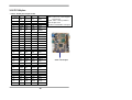
1
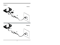
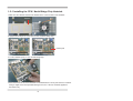
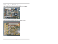
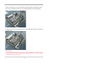
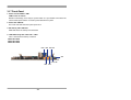
CI852A
400MHz FSB / VGA / LAN / Sound / Mini PCI /PC 104 Plus
400MHz FSB . All-in-one .
Sound . LAN . Mini PCI . PC 104 Plus
ATA 33/66/100 . 6 USB . CF
Multi-Lan Board
NO. CI852A
Release date: Sep . 30 . 2005
Contents
CI852A
CHAPTER 1 GENERAL INFORMATION ........................................................................ 1
1-1 MAJOR FEATURE........................................................................................................ 2
1-2 SPECIFICATION .......................................................................................................... 3
1-3 HARDWARE NOTICE GUIDE ..................................................................................... 4
1-3-1 INSTALLING THE CPU / NORTH BRIDGE CHIP HEATSINK.................................. 6
1-3-2 INSTALLING THE PC104 PLUS MODULE............................................................... 8
1-3-3 INSTALLING THE MINI PCI CARD.......................................................................... 10
1-3-3.1 REMOVING THE MINI PCI CARD........................................................................ 12
1-4 PACKING LIST*............................................................................................................13
CHAPTER 2 HARDWARE INSTALLATION ...................................................................14
2-1 UNPACKING PRECAUTION .......................................................................................14
2-2 UNPACKING CHECKUP .............................................................................................15
2-3 DIMENSION ................................................................................................................ 16
2-4 LAYOUT ...................................................................................................................... 17
2-5 DIAGRAM ....................................................................................................................18
2-5-1 BOTTOM SIDE DIAGRAM....................................................................................... 19
2-6 INSTALL MEMORY .................................................................................................... 20
2-7 LIST OF JUMPERS .................................................................................................... 21
2-8 JUMPER SETTING DESCRIPTION .......................................................................... 22
2-9 CMOS DATA SET ....................................................................................................... 22
2-10 JCF2 CF CARD POWER VOLTAGE SELECT ......................................................... 23
2-11 JCF1 CF CARD MASTER/ SLAVE SELECT ........................................................... 24
2-12 JV1: PANEL POWER SELECT ................................................................................ 24
CHAPTER 3 CONNECTION ........................................................................................ 25
3-1 LIST OF CONNECTORS............................................................................................ 25
3-2 FAN CONNECTOR ..................................................................................................... 26
3-3 IDE CONNECTORS ................................................................................................... 26
3-4 COMPACT-FLASH MEMORY SOCKET .................................................................... 28
3-5 SERIAL PORT CONNECTOR/VGA CONNECTOR.................................................... 29
3-6 KEYBOARD AND MOUSE CONNECTOR.................................................................. 30
3-7 USB PORT / HEADER .............................................................................................. 31
3-8 LAN PORT ................................................................................................................. 32
3-9 LVDS INTERFACE CONNECTOR ............................................................................. 34
3-10 PANEL POWER CONNECTOR ................................................................................ 34
3-11 DC 12V IN AND DC OUT........................................................................................... 35
3-12 DC +5/+12V OUTPUT CONNECTOR....................................................................... 36
i
3-13 AUDIO PORT CONNECTOR................................................................................... 37
3-14 WDT/DIO FUNCTION PORT (option)...................................................................... 38
2
3-15 I C BUS CONNECTOR............................................................................................ 39
3-16 PC104 PLUS............................................................................................................. 40
3-17 FRONT-PANEL.......................................................................................................... 41
CHAPTER 4 INTRODUCTION OF BIOS...................................................................... 42
4-1 ENTER SETUP .......................................................................................................... 42
4-2 GETTING HELP ......................................................................................................... 43
4-3 THE MAIN MENU ....................................................................................................... 43
4-4 STANDARD CMOS FEATURES ................................................................................ 45
4-5 ADVANCED BIOS FEATURES .................................................................................. 46
4-6 ADVANCED CHIPSET FEATURES ........................................................................... 47
4-7 INTEGRATED PERIPHERALS .................................................................................. 49
4-7-1 OnCHIP IDE DEVICE............................................................................................... 50
4-7-2 ONBOARD DRIVER FUNCTION............................................................................. 51
4-7-3 ONBOARD SUPER IO DEVICE ............................................................................. 52
4-8 POWER MANAGEMENT SETUP .............................................................................. 53
4-9 PNP / PCI CONFIGURATION SETUP ....................................................................... 55
4-10 PC HEALTH STATUS ............................................................................................... 56
4-11 FREQUENCY/VOLTAGE CONTROL ....................................................................... 57
4-12 LOAD OPTIMIZED DEFAULTS ................................................................................ 57
4-13 SET SUPERVISOR/USER PASSWORD ................................................................. 58
CHAPTER 5 DRIVER & FREE PROGRAM INSTALLATION...................................... 59
5-1 INF INSTALL INTEL 852/855 CHIPSET SYSTEM DRIVER ...................................... 61
5-2 VGA INSTALL INTEL 852/855 VGA DRIVER ............................................................ 62
5-3 SOUND Install VIA AUDIO CODEC ....................................................................... 63
5-4 HOW TO DISABLE ON-BOARD SOUND .................................................................. 64
5-5 HOW TO UPDATE BIOS ........................................................................................... 64
APPENDIX A: POWER CONSUMPTION TEST.............................................................. 65
APPENDIX B: BIOS SETUP FOR IDE STORAGE........................................................... 66
ii
2005
OCT. 21 . 2005
Chapter-1
General lnformation
The CI852A is a NEO form factor All-In-One Network control Board. The board's design
combines all necessary input and output effects interfaces, which makes itself an ideal
all-in-one control board for demanding network applications. CI852A is the perfect
platform for a whole range of small form factor, low-power network devices.
The CI852A's Intel 852GM chipset features Dual independent pipe for dual independent
display . It supports same images and native display timings on each display device.
It also support Improved hardware motion compensation for MPEG2, all format decoder
(18 ATSC formats) supported , Dynamic Bob and Weave support video streams.
Software DVD at 60 Fields/second and 30 frames / second full screen
With the sizable memory bandwidth of DDR266 SDRAM and the high data transfer speeds
of ATA/100, CI852A ensures the high performance levels required of today's most popular
digital Networking applications.
CI852A is supported with up to four 10/100/1G Ethernet for seamless broadband connectivity.
With Wake On LAN function and the PXE function in BIOS for Realtek LAN chipset only,
CI852A is a perfect control board for network devices. The built-in LAN options are
four Intel 82541GI/PI/ER with RJ45 for 10/100M/1Gbps Ethernet or four
Realtek RLT8110SB chipsets for 10/100M/1Gbps Ethernet; or another option of four Realtek
RLT8100C 10/100Mbps Ethernet.
Except CompactFlash, and a PC104Plus and Mini PCI slot, CI852A can integrate with
various type PC104Plus Card / Mini PCI Card. In addition, with the 6 hi-speed USB version 2.0
enhanced host controller interface, the CI852A ensures the high performance level and
also the powerful and flexible expansion.
With Ultra DMA-100/66 access of mode 4 to IDE drive interface architecture, the IDE
supports maximum 100MB/sec in data transfer rating to four enhanced IDE devices.
The CI852A All-In-One motherboard supports DDR memory with one DIMM socket up to 1GB.
Compact Flash reader supports IDE/ATA interface. A single Flash chip holds the system BIOS,
and you can change the Flash BIOS by the Utility Update. Advanced IR port also provides a
faster data transmission.
The CI852A All-In-One motherboard is fully compatible with industry standards,
plus technical enhancements, and thousands of software applications developed for
IBM PC/AT compatible computers. The control logic provides high-speed performance
for the most advanced multi user and multitasking applications available today.
1
1-1 Major Feature
1. Intel Celeron M 600 Mhz L2 0K CPU on board ( FSB 400 Mhz )
2. Intel 82852GM Chip Set on board , Graphic Chip Integrated
3. Support DDR 200 / 266 up to 1GB
4. Support 4 x 10 / 100 M LAN on Board ( Intel / Realtek LAN Chip ) , Giga LAN is option ,
Support PXE / RPL Function (for Realtek LAN only)
5. Support up to 64 MB Video Memory ( Share from System Memory )
6. 18 bits LVDS Interface on Board , Support up to UXGA Resolution /
Support Twin View Function .
7. Support 1 x 40 Pins IDE + 1 x 44 Pins IDE and 1 x Compact Flash Card Socket
on Board ( All can be Boot-Up Device )
8. Support PC104Plus Socket on board , up to 4 pcs PC104Plus Card /
Mini PCI Socket on board (Note: -5V, -12V no support)
9. External +12V Power Supply
10. Compact PCB Dimension : 200 x 150 mm
11. Support MS Windows 9x / ME / 2k / XP / CE / XP Embedded , Linux 2.4
*The models mentioned above are standard models currently.
2
1-2 Specification
1. CPU : Intel Celeron M 600 Mhz
2. Cache Memory : L1 32KB , L2 0KB
3. ChipSet : Intel 82852GM and Intel 82801DB ICH4
4. Memory : One Dimm socket up to 1GB DDR
5. VGA : Internal Graphics Memory Up to 64MB of dynamic video memory allocation
6. I/O Chip : ITE IT8712F (IX)IO
7. IDE : Ultra ATA 100/66/33,BMIDE and PIO mode
8. LAN : 4 x Realtek RLT8100C 10T/100T
4 x Realtek RLT8110SB 10T/100T/Giga
4 x Intel 82541GI 10/100T/Giga
9. Storage Device : 1 x 50 pins Compact Flash Socket
1 x 40 pins IDE
1 x 44 pins IDE
10. Serial Port : 1 x RS232
11. USB : 6 x USB 2.0
12. Keyboard : PS/2 5pins Header
13. Mouse : PS/2 5pins Header
14. Sound : AC'97 2.1 ,
15. BIOS : Award BIOS version V6.00PG
16. Form Factor : Light Board , 200 x 150 mm
17. Power : DC 12V-In
18. Power Voltage : +12V +- 5%
19. Power Consumption: Please refer to page 65
3
1-3 Hardware Notice Guide
1. Before installing the power supply with this motherboard, please attach the 12V/DC
( 4 pin connector )of the adapter to motherboard first.
After that, plug the adapter power to AC outlet.
Always normally shut down the computer before you move the system unit or remove
the power supply from the motherboard.
Please unplug the 12V/DC ( 4 pin connector ) of the adapter from motherboard first.
Then unplug the adapter from the AC outlet.
Please refer to procedure from the photo 1
2. There will be high possibility to burn out the CPU if you change/ modify any parts of the
CPU cooler.
3. Please wear wrist strap and attach it to a metal part of the system unit before handling a
component.
You can also touch an object that is of ground connection or with metal surface if you don't
have wrist strap.
4. Please be careful when you handle this product. Pay attention to & don't touch the
sharp-pointed components at the bottom PCB .
5. Please pay attention to this: Remove or change any components form the motherboard
will VOID the warranty of the motherboard you purchased .
6. Before you install/remove any components or make any jumper setting on the motherboard,
please make sure to disconnect the power first.
( Please follow the instructions as of this guide )
7. Please only use single sided Mini PCI card, do not use the double sided Mini PCI card
which is not suitable.
8. This does not support 16 bit mini PCI card
9. Please follow this instruction carefully when using the "POWERON after PWR-Fair" function.
When the DC power adaptor runs out of power, unplug it from the DC current;
when power returns plug it back in only after 5 seconds. If there is a power outage,
unplug it from the AC current, when power returns plug it back in only after 30 seconds.
Otherwise it will cause system locking or serious damage.
Remark 1:
Always insert/unplug the 12V/DC ( 4 pin connector ) horizontally & directly from the
motherboard.
DO NOT twist the 12V/DC ( 4 pin connector ) gently, it is designed to fit snugly .
Moreover, erratic pull / push testing with the DC Jack might cause the unpredictable
damage to the component & system unit.
4
Photo 1
Insert
1
2
3
Unplug
1
2
3
5
1-3-1 Installing the CPU / North Bridge Chip Heatsink.
1.Make sure the Heatsink washers are attached to the correct location of the Heatsink.
washers
2. Apply the thermal pad on center part of CPU and North Bridge chip.
thermal pad
3. Put the Heatsink gently on CPU & North Bridge chip
4.Press the latches to secure the Heatsink on the Motherboard. Never push down the Heatsink.
Doing so might cause the irreparable damage to the CPU. All force should be applied to
the latches only.
6
5. Make sure all Heatsink latches are firmly aligned with the motherboard.
6. Connect cooler's fan power cable onto CPUFAN (JF2) connector.
Important Note :
1. The CPU and North Bridge chip will suffer thermal failure with improper Heatsink installation.
The system will automatic power off when the CPU is reaches the temperature of 110 C
2. Wrong location of Heatsink washer and improper force while installing Heatsink might
cause irreparable damage to CPU and Northe Bridge chips and such damage will
VOID warranty service.
0
7
1-3-2 Installing the PC104 Plus Module
1.Make sure there are 4 pcs copper risers before installing the PC104 Plus Module
2. Make sure there are no crooked or missing pins of PC104 Plus connector.
8
3. Press down firmly on the PC104 Plus module until the module is completely seated in
the connector. (Repeat this step if you are installing additional PC104 Plus Modules. )
4. Secure PC104 Plus module with screws and stack additional PC104 Plus modules with
copper risers.
Important Note :
1. Do not tilt and be careful not to bend any pins while installing the PC 104 Plus module.
2. Improper installation might cause irreparable damage to the pins or connector and such
damage will VOID warranty service.
9
1-3-3 Installing the Mini PCI card
1. Align the Mini PCI card with the connector at a 45 degree angle.
2. Press the Mini PCI into the connector until you hear a click.
10
Notices:
1.The connectors are designed to ensure the correct insertion. If you feel resistance, check the
connectors & golden finger direction, and realign the card.
2. Make sure the retaining clips (on two sides of the slot) lock onto the notches of
the card firmly.
11
1-3-3.1 Removing the Mini PCI card
1. Release the Mini PCI card by pulling outward the two retaining clips and the card
pops up slightly.
2. Lift the mini PCI card out of its connector carefully.
12
1-4 Packing List*
1 CI852A Board
5 Power Cable
2 DC 12V Power Adapter (4P)
6 Utility CD Disk
3 One ATA 100 Flat Cable
7 User's Manual
4 One slim IDE port flat Cable (2.0mm)
3
4
2
1
6
5
7
*The packing list above is for the users who purchase single motherboard. The users
who purchase the board with chassis may refer to the packing list in the Assembly Guide.
Please contact your dealer if any of these items is missing or damaged
on delivery. And please keep all parts of the package with packing
materials in case you need to deliver or store the product in the future.
13
Chapter-2
Hardware Installation
This chapter provides the information how to install the hardware of CI852A.
Please follow section 1-3, 2-1 and 2-2 to check the delivery package and unpack
carefully. Please follow the jumper setting procedure.
2-1 Unpacking Precaution
The CI852A board has been well packed with an anti-static bag to protect its sensitive
components and circuitry from damage due to static electric discharge.
NOTE!
1. Do not touch the board or any other sensitive components without all necessary
anti-static protection.
2. Please pay attention to the voltage limitation of DC-IN12 V +- 5 %.
Overuse of DC-IN voltage limitation or change to another power adapter
( not provided with this system ) will VOID warranty.
You should follow these
steps to protect the board from the static electric
discharge whenever you handle the board:
1. Ground yourself by a grounded wrist strap at all times when you handle the CI852A.
Well secure the ALLIGATOR clip of the strap to the end of the shielded wire lead from
a grounded object. Please put on and connect the strap before handling the CI852A
for harmlessly discharge any static electricity through the strap.
2. Please use anti-static pad to put any components, parts, or tools on the pad whenever
you work on them outside the computer. You may also use the anti-static bag instead of
the pad. Please ask your local supplier for necessary parts on anti-static requirement.
3. Do not plug any connector or set any jumper when the power is on.
14
2-2 Unpacking checkup
First of all, please follow all necessary steps of section 2.1 to protect CI852A
from electricity discharge. With reference to section 1.3, please check the delivery package
again with following steps:
1. Unpack the CI852A board and keep all packing material, manual
and driver disc etc, do not dispose !
2. Is there any components lose or drops from the board? DO NOT CONTINUE
TO INSTALL THIS BOARD!CONTACT THE DEALER YOU PURCHASED THIS
BOARD FROM, IMMEDIATELY.
3. Is there any visible damage on the board? DO NOT CONTINUE TO INSTALL
THIS BOARD!CONTACT THE DEALER YOU PURCHASED THIS
BOARD FROM, IMMEDIATELY.
4. Check your optional parts (i.e. DDR, CF etc.), all necessary jumpers
setting to jumper pin-set, and CMOS setup correctly.
Please also refer to all information of jumper settings in this manual.
5. Check your external devices (i.e. Add-On-Card, Driver Type etc.)
for complete add-in or connection and CMOS setup correctly.
Please also refer to all information of connector connection in this manual.
6. Please keep all necessary manual and driver disc in a good condition for future
re-installation if you change your Operating System.
15
2-3 Dimension
34.00
200x150(mm)
190.00
170.59
153.15
135.97
118.78
92.50
64.05
19.10
35.70
10.50
5.10
rj45
rj45
4x
rj45
6.71
5.10
133.40
122.94
120.40
92.44
6.71
42.9
29
93
3
46.74
92.44
172.10
187.37
192.90
16
14.33
15.00
19.10
158.90
2-4 Layout
CN26
CN3
CN12
JSW1
JF2
CN21
JP1
DC IN 12V
CN5
SW1
JPL1
Power LED
HD LED
LED1
LED2
LED3
LED4
CN1
JF1
CN7
JV1
CN11
JC1
CN13
CN6
DIMM1
BATTERY
JI1
JB1
CN15
CN10
JCF2
CN9
JCF1
CN8
CN24
CN23
CN4
CN20
CN22
JUSB1
CN14: PC104+
Optional
CN2
CN19
CN25
CN16
CN17
CN18
17
2-5 Diagram
CN3
CN26
JF2
JSW1
CN12
CN21
CN13
JP1
SW1
JPL1
CN1
PW LED
HD LED
LED1
LED2
LED3
LED4
JF1
CN7
JV1
CN11
JC1
DIMM1
CN6
BATTERY
JI1
JB1
CN15
CN10
CN9
JCF2
JCF1
CN8
CN24
CN4
CN23
CN20
CN22
CN2
CN25
CN14: PC104+
Optional
18
CN16
CN17 CN19
CN18
JUSB1
2-5-1 Bottom Side Diagram
MPCI: Mini PCI Socket
Back Panel
USB
VGA
RJ45 LAN2
COM
DC 12V IN
PS/2 Mouse
RJ45 LAN1
PS/2 Keyboard
19
RJ45 LAN4
RJ45 LAN3
Line-Out
2-6 Install Memory
This motherboard provides one 184-pin DUAL INLINE MEMORY MODULES (DIMM)
socket for memory expansion available from minimum memory size of 64MB to
maximum memory size of 1GB DDR RAM.
Supports PC 1600/2100 DDR DIMM, DRAM clock supports: DDR200, DR266
Mixed 1M / 2M / 4M / 16M / 32M / 64M x N DRAMs
Valid Memory Configurations
Total Memory
DIMM1
System Accept or Not
DS/SS
Accept
Min. ~ Max.
64MB~1GB
SS: Single Sided DIMM
DS: Double Sided DIMM
NOTE!
Make sure the total installed memory does not exceed 1GB;
otherwise, the system may hang during startup.
DIMM1 (BANK0+BANK1)
Install DDR RAM module oriented as Fig. 2.1.
Figure 2.1
20
NOTE!
When you install DIMM module fully into the DIMM socket, the eject tab should be
locked into the DIMM module very firmly and fit into its indention on both sides.
WARNING!
1. If the DDR RAM CLOCK is set at 133MHz, you must use DDR266-compliant
DIMMs. When this motherboard operates at 133Mhz, the system will not boot
if non DDR266-compliant DDR RAM modules are used because of
the strict timing issues.
2. Once you hear " Beep Beep Beep" sounds after turning on the power ,
please check if the DRAM is installed properly or not.
2-7 List of Jumpers
JB1: CMOS DATA SET
JCF2: CF card Power +5V/+3.3V select
JCF1: CF card master and slave select
JV1: LVDS power select
21
2-8 Jumper Setting Description
A jumper is ON as a closed circuit with a plastic cap covering two pins. A jumper is OFF as an
open circuit without the plastic cap. Some jumpers have three pins, labeled 1, 2, and 3.
You could connect either pin 1 and 2 or 2 and 3.
The below figure 2.2 shows the examples of different jumper settings in this manual.
Figure 2.2
All jumpers already have its default setting with the plastic cap inserted as ON,
or without the plastic cap as OFF. The default setting may be referred in this
manual with a " " symbol .
*
2-9 CMOS Data Set
A battery must be used to retain the motherboard configuration in CMOS RAM.
Close pin 1and pin 2 of JB1 to store the CMOS data.
To clear the CMOS, follow the procedures below:
1. Turn off the system and unplug the AC power
2. Remove DC 12V power cable from DC 12V power connector
3. Locate JB1 and close pin 2-3 for a few seconds
4. Return to its normal setting by shorting pin 1-2
5. Connect DC 12V power cable back to DC 12V power connector
22
Note: Do not clear CMOS unless
1. Troubleshooting
2. Forget password
3. You fail over-clocking system
JB1
*1-2
2-3
Description
*Normal Set
CMOS Data clear
JB1
3
2
1
*Normal
3
2
1
Clear Setting
2-10 JCF2 CF Card Power Voltage select
If you use CF card and HDD together, we suggest you
use the jumper setup for +5V.
JCF2
Description
*1-2
*For CF CARD power voltage select +5V
2-3
For CF CARD power voltage select +3.3V
JCF2
1 2 3
+5V*
* We use
to refer to as pin1
23
1 2 3
3.3V
2-11 JCF1 CF Card Master/Slave selection
If you use CF card and HDD together, please set CF as Master and HDD as Slave.
JCF1
Description
*1-2
*CF Card use Master type
2-3
CF Card use Slave type
JCF1
1 2 3
1 2 3
Master*
Slave
2-12 JV1: Panel power select
JV1
Description
1-2
+5V
*2-3
+3.3V
JV1
3
2
1
+3.3V*
3
2
1
+5V
24
Chapter-3
Connection
This chapter provides all necessary information of the peripheral's connections,
switches and indicators. Always power off the board before you install the peripherals.
3-1 List of Connectors
CN3: DC 12V-IN DIN Connector
CN5: DC 12V-IN Connector
CN26:DC 12V-IN Connector
CN1: VGA DB15 Connector
CN1: PS2 Keyboard Connector
CN1: PS2 Mous Connector
CN7: USB Connector
CN6: COM1 port Connector
JC1: COM1 port Connector
CN10: RJ45 LAN1 Jack
CN9: RJ45 LAN2 Jack
CN8: RJ45 LAN3 Jack
CN4: RJ45 LAN4 Jack
CN25:LAN Link LED
CN2/24: Line out connector
CN23: MIC-IN Connector
CN22: USB 4 port connector
JUSB1/JUSB2:USB 4/5 port connector
CN13: LVDS connector
CN12 : Inverter power connector
CN18: IDE1 (2.54mm)Connector
CN16: IDE2 (2.0mm)Connector
CN15 : CF socket
CN17: DC +5/+12V output connector
CN20: CD-IN Header
CN19: Line-IN Header
JI1: IR connector
JF2: CPU FAN connector
JF1: System FAN connector
CN11 : DIO connector
CN21: I2C Bus connector
CN14 : PC104 plus socket
MPCI1:Mini PCI socket
25
3-2 FAN Connector
CI852A provides one CPU fan connector and one system fan connector.
CPU Fan Connector- JF2
PIN NO.
Description
System FAN Connector-JF1
1
FAN Control ON/OFF
JF2
pin1
JF1
2
+12V
3
FAN speed Sensor
pin1
*Note : DC- in +12V by switch to DC-out voltage +12V
So DC -in need stable +12V input
3-3 IDE Connectors
PIN NO.
There are two kinds of IDE connectors on this
board, 40-pin and 44-pin. Each can support up
to two IDE-inferface devices. One standard
40-pin header daisy-chain driver connector
provides as IDE1 with following pin assignment.
40 pins (2.54mm)-CN18(IDE 1)
This connector supports the provided IDE hard
disk ribbon cable. After connecting the single
plug end to motherboard, connect the two
plugs at other end to your hard disk(s). If you
install two hard disks, you must configure the
second drive as Slave mode by setting its
jumpers accordingly. Please refer to the
documentation of your hard disk for the
jumper settings.
Description
PIN NO.
Description
1
RESET#
2
GROUND
3
DATA7
4
DATA8
5
DATA6
6
DATA9
7
DATA5
8
DATA10
9
DATA4
10
DATA11
11
DATA3
12
DATA12
13
DATA2
14
DATA13
15
DATA1
16
DATA14
17
DATA0
18
19
GROUND
20
21
DREQ
22
DATA15
+5V
GROUND
23
IOW#
24
GROUND
25
26
28
GROUND
27
IOR#
IORDY
29
DACK#
GROUND
31
IRQ14/15
30
32
33
SA 1
34
ATA 33/66/100
CABLE SELECT
PULL DOWN
NC
35
SA 0
36
SA 2
37
HD CS0#
38
HD CS1#
39
HD LED
40
GROUND
Note: Pin20 is +5V power can use new type DOM module.
26
44 pins(2.0mm)-CN16 (IDE2)
This connector supports slim type 2.5" HDD. Follow the same procedure described for the
primary IDE connector. You may also configure two hard disks as both Masters using one
ribbon cable on the primary IDE connector and another ribbon cable on the secondary
IDE connector. (See Appendix B)
PIN NO.
Description
PIN NO.
Description
1
RESET#
2
GROUND
3
DATA7
4
DATA8
5
DATA6
6
DATA9
7
DATA5
8
DATA10
9
DATA4
10
DATA11
11
DATA3
12
DATA12
13
DATA2
14
DATA13
15
DATA1
16
DATA14
17
DATA0
18
19
GROUND
20
21
DREQ
22
DATA15
NC
GROUND
23
IOW#
24
GROUND
25
26
28
GROUND
27
IOR#
IORDY
29
DACK#
GROUND
31
IRQ14/15
30
32
33
35
37
SA 1
SA 0
39
41
43
HD CS0#
HD LED
34
36
38
Note!
PIN 20 connector +5V of
IDE 1 could provide the
power of DOM
PULL DOWN
NC
ATA 33/66/100 CABLE SELECT
SA 2
HD CS1#
40
GROUND
+5V
42
+5V
GROUND
44
NC
IDE2
IDE1
pin1
CN18 (IDE1)
pin1
CN16 (IDE2)
27
3-4 Compact - Flash Memory Socket
CI852A configures CompactFlash Storage Card in IDE mode. It will use IDE channel when
CompactFlash card is plugged in. This socket supports CF Card Type I/II socket spec.
CF Socket 50pin----CN15
PIN NO.
Description
PIN NO.
Description
1
GND
26
-CD1
2
DATA3
27
DATA11
3
DATA4
28
DATA12
4
DATA5
29
DATA13
5
DATA6
30
DATA14
6
DATA7
31
DATA15
7
-CS0
32
-CS1
8
NC(A10)
33
-VS1
9
-ATA SEL
34
10
NC(A9)
35
11
NC(A8)
36
-IOR
-IOW
-WE(PH)
12
NC(A7)
37
INTR
13
38
39
VCC
14
VCC
NC(A6)
15
NC(A5)
NC(-VS2)
16
NC(A4)
40
41
17
NC(A3)
42
IORDY
18
SDA2
43
NC
19
20
SDA1
SDA0
44
-REG(PH)
-DASP
21
DATA0
22
23
24
25
-CSEL
RESET
45
46
-PDIAG
DATA1
47
DATA8
DATA2
-IOCS16
48
49
50
DATA9
DATA10
GND
-CD2
CN15
Note * : Refer JCF1 /JCF2 Jumper set
28
3-5 Serial Port Connector / VGA Connector
CN6: COM1 DB9 Connector up side (D SUB 9PIN )
RS232 Mode
PIN NO.
Description
PIN NO.
Description
1
DCD
2
3
TXD
4
RXD
DTR
5
GND
6
DSR
7
RTS
8
CTS
9
RI
10
NC
JC1: COM1 TX/RX Connector --- 5pin(1.25mm Wafer connector)
PIN NO.
Description
1
2
3
4
5
+5V
GND
RTS
TX
RX
CN1: VGA DB15 Connector down side (D SUB 15PIN)
PIN NO.
Description
PIN NO.
Description
PIN NO.
Description
1
RED
6
GND
11
NC
2
GREEN
7
GND
12
DDC DATA
3
BLUE
8
GND
13
H-SYNC
4
NC
9
NC
14
V-SYNC
5
GND
10
GND
15
DDC CLOCK
VGA-CN1
JC1
pin1
COM1-CN6
29
3-6 Keyboard and Mouse Connector
CN1: PS2 Keyboard down side (Din 6 pin jack)
PIN NO.
Description
1
KB DATA
2
NC
3
GND
4
5
6
+5V
KB CLOCK
NC
CN1: PS2 Mouse down side (Din 6 pin jack)
PIN NO.
Description
1
MS DATA
2
NC
3
GND
4
5
6
+5V
MS CLOCK
NC
CN1
PS/2 Keyboard
CN1
PS/2 Mouse
30
3-7 USB Port/ Header
CN22: USB 4 port Type A Jack
CN7: USB 0/1/2/3 port Type A Jack
PIN NO.
Description
PIN NO.
Description
1
+5V
1
+5V
2
USB DATA0/1/2/3-
2
USB DATA 4-
3
USB DATA0/1/2/3+
3
USB DATA 4+
4
GND
4
GND
JUSB1/JUSB2 USB 4/5 port Connector(2.54mm)
PIN NO.
Description
1
+5V
2
USB DATA4/5-
3
USB DATA4/5+
4
KEY
5
GND
CN22
pin1
CN7
31
JUSB1
3-8 LAN Port
The Fast Ethernet controller provides 32-bit performance, PCI bus master capability, and full
compliance with IEEE 802.3 10/100Based-T specification.
For 10/100Base-T operation, please connect the network connection by plugging one end of
the cable into the RJ-45 jack of the CN10,CN9,CN8,CN4 Connector.
Besides 10/100 Base-T, CI852A can provide Giga LAN solution through CN10,CN9,CN8,CN4
once equipped with Intel 82541GI/PI/ER chipset.
.
RJ45 LAN Connector--- CN10/9/8/4 RJ45 Giga/100MB Connector
PIN NO.
.
Description
PIN NO.
Description
1
TD0-/TX+
5
2
TD0+/TX-
6
TD2-/NC
TD2+RX-
3
TD1-/RX+
7
TD3-/NC
4
TD1+NC
8
TD3+/NC
CN4: Giga/100Mb LAN4 Header (2x4 Header 2.0mm) (for option use)
PIN NO.
Description
PIN NO.
Description
1
TD0-/TX+
5
TD0-/TX+
2
TD1+NC
6
TD2+RX-
3
TD2-/NC
7
TD1-/RX+
4
TD3+/NC
8
TD3+/NC
RJ45 CN10
RJ45 CN9
32
RJ45 CN8
RJ45 CN4
LAN Led
RJ45 LAN Connector--- LED define Giga/100/10MB Conector
Back side connector
RED LED
GREEN LED
YELLOW LED
Indicate
GIGA LAN
Link(light)
100Mb LAN
Link(light)
10Mb LAN
Link(light)
Fron side
LAN1/2/3/4 or LAN1 LED Header
Indicate
LAN10/100/1000BT Actived (light)
RJ45 LAN Connector--- LED define 10/100MB Conector
Back side connector
Indicate
GREEN LED
YELLOW LED
100Mb LAN
Link(light)
10Mb LAN
Link(light)
Fron side
LAN1/2/3/4 or LAN1 LED Header
Indicate
LAN10/100BT Actived (light)
CN25: LAN link LED (2x4 Header 2.0mm)
PIN NO.
Description
PIN NO.
Description
1
LAN1 LED+
2
LAN1 LED-
3
LAN2 LED+
4
LAN2 LED-
5
LAN3 LED+
6
LAN3 LED-
7
LAN4 LED+
8
LAN4 LED-
CN25
pin1
33
3-9 LVDS Interface Connector
CN13: LVDS interface connector
Digital Front Panel interface connector (2x15 pin wafer 1.25mm)
PIN NO.
Description
PIN NO.
1
DDC-CLK
2
3
NC
4
Description
DDC-DATA
NC
5
Channel-1-DATA3+
7
Channel-1-DATA3-
8
Channel-0-DATA3-
9
Channel-0-DATA2+
10
Channel-0-CLK+
11
Channel-0-DATA2-
12
Channel-0-CLK-
13
GND
Channel-0-DATA3+
14
15
Channel-0-DATA1+
17
Channel-0-DATA1GND
19
6
GND
16
Channel-0-DATA0+
18
Channel-0-DATA0GND
+LCD(5Vor 3.3V)*
20
22
21
+LCD(5Vor 3.3V)*
23
Channel-1-DATA2+ 24
Channel-1-CLK+
25
27
29
Channel-1-DATA2-
26
Channel-1-CLK-
30
Channel-1-DATA0+
Channel-1-DATA1+ 28
Channel-1-DATA1- 30
Channel-1-DATA0-
Note * : Refer JV1 Jumper set
pin1
3-10 Panel Power Connector
CN13
CN12: Panel Power Connector --- 1x5Pin (2.0mm)
PIN NO.
Description
1
+12V
2
3
4
5
GND
BRIGHT
GND
ENBKL
PIN 3 default pull Low
Note :
DC-in +12V by switch to LVDS Inverter power +12V
So DC-in need stable +12V input
pin1
CN12
34
3-11 DC 12V IN and DC out
. CN3: DC 12V-IN Connector (4pin mini den connector)
PIN NO.
Description
1,2
+12V DC-IN
3
NC
4
GND
. CN5: DC 12V-IN Internal Connector (4pin connector) ( For option connector)
PIN NO.
Description
3,4
+12V DC-IN
1,2
.
GND
CN26: DC 12V-IN Internal Connector (2pin Wafer 2.0mm)
PIN NO.
1
2
Description
+12V DC-IN
GND
! Danger : CN26 voltage from DC-in Voltage
CN3
DC 12V IN
35
3-12 DC +5/+12V output connector
. CN17 : DC +5/+12V output connector(2.5mm Wafer)
PIN NO.
Description
1
+5V
2
GND
3
GND
4
+12V*
pin1
CN17
36
3-13 Audio Port Connector
The CI852A has an on-board AC'97 3D sound interface. There are the connectors of
LINE OUT, MIC-IN and CD-IN connectors.
The MIC-IN Jack and CD-IN header are for audio sound input. The LINE-OUT
connector is a 4-pin Jack for audio sound output.
CN2/CN24: Speak out connector
. CN24(Phone Jack) -----Line-OUT
(3.5mm Phone jack or 5pin 2.54mm header)
.
CN23 (Phone Jack) -----MIC-IN
(3.5mm Phone jack or 5pin 2.54mm header)
PIN NO.
Description
PIN NO.
Description
1
GND
1
GND
2
FRONT OUT-L
2
MIC-PW
3
NC
3
GND
4
NC
4
NC
5
FRONT OUT-R
5
MIC-IN
CN2 share to CN24
Speak out CN24
MIC-IN CN23
.
CN20 (2.54mm 4pin header)-----CD-IN
PIN NO.
Description
1
CD-L
2
GND
3
GND
4
CD-R
.
CN19 (2.54mm 4pin header)-----LINE-IN
PIN NO.
Description
1
Line in-L
2
GND
3
GND
4
Line in-R
pin1
CN20
pin1
CN19
37
3-14 WDT/DIO Function port (Option)
. CN11: WDT/DIO option Function port (2 x 5 2.0mm Header)
Digital 4 Input and 4 Output Connector
PIN NO.
Description
1
DI-0
PIN NO.
2
DO-3
Description
3
DI-1
4
DO-2
5
DI-2
6
DO-1
7
DI-3
8
DO-0
9
GND
10
+5V
Software Port Address For DIO Description
Write port 60C H
Bit 3
Bit 2
Bit 1
Bit 0
PIN NO (OUTPUT)
DO-3
DO-2
DO-1
DO-0
pin10
CN11
Logic 0 Level :+0.5V Max , Logic 1 Level : +4V Min
pin1
Read port 608H
Bit 3
Bit 2
Bit 1
Bit 0
PIN NO (INPUT)
DI-3
DI-2
DI-1
DI-0
Logic 0 Level :+0.5V Max , Logic 1 Level : +4V Min
Software Port Address For WDT/DIO Description
Software Port address
600H
604H
DESCRIPTION
ENABLE WDT Timer 0-255 Sec.
DISABLE WDT Timer
The system will reset .when WDT is enable, and the hardware start down counter reaches zero
Follow test:
>debug
-O 600 01 ; Enable WDT 00-FF 00sec to 255 sec
-I 604
; Disable WDT
-O 60C 0F ; Output DO 0-3 all Hi level ,(DO 4 -7 no use)
-I 608
; Input DI 0-3 all Hi level ,(DI 4 -7 no use)
-0F
; DI 0 - 3 all pin is Hi
38
2
3-15 I C Bus connector
. CN21: I C Bus connector 4pin (1.25mm Wafer connector)
2
PIN NO.
1
Description
+3.3V
2
GND
3
I2C CLK
4
I2C DATA
pin1
CN21
39
3-16 PC104 plus
. CN14 : PC104 plus 120 pin socket
PIN NO.
1
A
GND
B
C
D
Reserved
+5V
AD00
2
VI/O
AD02
AD01
+5V
3
AD05
GND
AD04
AD03
4
C/BE0#
AD07
GND
AD06
5
GND
AD09
AD08
GND
6
AD11
VI/0
AD10
M66EN
7
AD14
AD13
GND
AD12
8
+3.3V
C/BE1#
AD15
+3.3V
9
SERR#
GND
Reserved
PAR
10
GND
PERR#
+3.3V
Reserved
11
STOP#
+3.3V
LOCK#
GND
12
+3.3V
TRDY#
GND
DEVSEL#
13
FRAME# GND
IRDY#
+3.3V
14
GND
AD16
+3.3V
C/BE2#
15
AD18
+3.3V
AD17
GND
16
AD21
AD20
GND
AD19
17
+3.3V
AD23
AD22
+3.3V
18
IDSEL0
GND
IDSEL1
IDSEL2
19
AD24
C/BE3#
VI/O
IDSEL3
20
GND
AD26
AD25
GND
21
AD29
+5V
AD28
AD27
22
+5V
AD30
GND
AD31
23
REQ0#
GND
REQ1#
VI/O
24
GND
REQ2#
+5V
25
GNT1#
VI/O
GNT2#
26
+5V
CLK0
GND
CLK1
27
CLK2
+5V
CLK3
GND
GNT0#
GND
28
GND
INTD#
+5V
RST#
29
+12V*
INTA#
INTB#
INTC#
30
NC(-12V) REQ3#
GNT3#
GND
40
Note : VI/O is +5V , Don't support
-12V and -5V
* Note : DC in +12V by switch to
PC 104 plus +12V
So DC in need stable +12V input
CN14 : PC104 plus
3-17 Front-Panel
1. Power switch: PW-ON--- SW1
JSW1: Power on switch
Based on case design , there may be a power switch or a 2-pin header connected to the
case-mounted power switch. It is used to power ON/OFF the system.
2. Power LED: PW-LED
The Power LED is lit while the system power is on.
3. IDE Activity LED: HDD-LED
HDD-LED shows the activity of the hard disk.
4. LAN LED Activity LED: LAN- LED----LED1
LAN 1 LED shows the activity of network
LAN2 LED--LED2
LAN3 LED--LED3
LAN4 LED--LED4
LED4
LED2 HDD LED
SW1
Power LED
LED3 LED1
41
Chapter 4
Introduction of BIOS
The BIOS is a program located in the Flash Memory on the motherboard.
This program is a bridge between motherboard and operating system.
When you start the computer, the BIOS program gains control. The BIOS first
operates an auto-diagnostic test called POST (Power on Self Test) for all the
necessary hardware, it detects the entire hardware devices and configures the
parameters of the hardware synchronization. After these tasks are completed,
BIOS will give control of the computer back to operating system (OS). Since the BIOS
is the only channel for hardware and software to communicate with, it is the key factor
of system stability and of ensuring your system performance at best.
In the BIOS Setup main menu of page 43, you can see several options. We will
explain these options in the following pages. First, let us see the function keys
you may use here:
..
.
.
Press <Esc> to quit the BIOS Setup.
Press (up, down, left, right) to choose the option you
want to confirm or modify.
Press <F10> to save these parameters and to exit the BIOS Setup menu after
you complet the setup of BIOS parameters.
Press Page Up/Page Down or +/- keys to modify the BIOS
parameters for the active option.
4-1 Enter Setup
Power on the computer and press <Del> immediately to enter Setup.
If the message disappears before your respond but you still wish to enter Setup,
restart the system by turning it OFF then ON button on the system case. You may
also restart the system by simultaneously pressing <Ctrl>, <Alt> and <Delete> keys.
If you do not press the keys at the proper time and the system does not boot, an
error message will display and you will be asked to
Press <F1> to continue, <Ctrl-Alt-Esc> or <Del> to enter Setup
42
4-2 Getting Help
Main Menu
The on-line description of the highlighted setup function is displayed at the
bottom of the screen.
Status Page Setup Menu/ Option Page Setup Menu
Press F1 to pop up a small help window that describes the appropriate keys to use
and the possible selections for the highlighted item.
To exit the Help Window, press <Esc>.
4-3 The Main Menu
Once you enter Award BIOS CMOS Setup Utility, the Main Menu will appear on the
screen. The Main Menu has fourteen setup functions and two exit choices.
Use arrow keys to select among these items. Press <Enter> to accept or enter
the sub-menu.
Phoenix-AwardBIOS CMOS Setup Utility
Standard CMOS Features
Frequency/Voltage Control
Advanced BIOS Features
Load Fail-Safe Defaults
Advanced Chipset Features
Load Optimized Defaults
Integrated Peripherals
Set Supervisor Password
Power Management Setup
Set User Password
PnP/PCI Configurations
Save & Exit Setup
PC Health Status
Exit Without Saving
Esc : Quit
↑↓→ ←
: Select Item
F10 : Save & Exit Setup
Time, Date, Hard Disk Type…
43
Standard CMOS Features
This Menu is for basic system configurations.
Advanced BIOS Features
This menu is to set the Advanced Features available in your system.
Advanced Chipset Features
This menu is to change the values in the chipset registers and optimize your
system performance.
Integrated Peripherals
This menu is to specify your settings for integrated peripherals.
Power Management Setup
This menu is to specify your settings for power management.
PnP/PCI configurations
This entry appears if your system supports PnP/PCI.
PC Health Status
This entry shows your PC health status.
Frequency/Voltage Control
This menu is to specify your settings for Miscellaneous Control.
Load Optimized Defaults
Use this menu to load the BIOS default values that are settings for optimal performances
system operations.
Set Supervisor/User Password
This menu is to set User and Supervisor Passwords.
Save & Exit Setup
Save CMOS values modified to CMOS and exit setup.
Exit Without Saving
Abandon all the CMOS values modified and exit setup.
44
4-4 Standard CMOS Features
The items in Standard CMOS Setup Menu are divided into several categories.
Each category includes, one or more than one setup items. Use the arrow
keys to highlight the item and then use the <PgUp> or <PgDn> keys to select
the value you want to modify with this item.
Phoenix - AwardBIOS CMOS Setup Utility
Standard CMOS Features
Date (mm:dd:yy)
Sat, Jan,
Time (hh:mm:ss)
0 : 0 : 0
IDE Primary Master
IDE Primary Slave
[ None ]
[ None ]
IDE Secondary Master
[ None ]
IDE Secondary Slave
[ None ]
Video
[EGA/VGA]
Halt On
[No
Base Memory
1 2005
Item Help
Menu Level >
Change the day, month,
year and century
Errors]
640K
Extended Memory
228352K
Total Memory
229376k
↑↓→←:Move Enter:Select +/-/PU/PD:Value F10:Save ESC:Exit F1:General Help
F5:Previous Values
F6:Fail-Safe Defaults
F7:Optimized Defaults
45
4-5 Advanced BIOS Features
Virus Warning
CPU L1 & L2 Cache
Quick Power On Self Test
First Boot Device
Second Boot Device
Third Boot Device
[Disabled]
[Enabled]
[Enabled]
[USB-FDD]
[USB-CDROM]
[HDD-0]
Boot Other Device
[Enabled]
Boot Up NumLock Status
Gate A20 Option
Typematic Rate Setting
[On]
[Fast]
X Typematic Rate (Chars/Sec)
X Typematic Delay (Msec)
OS Select For DRAM > 64MB
C8000- CBFFF Shadow
CC000-CFFFF Shadow
D0000-D3FFF Shadow
D4000-D7FFF Shadow
D80 00-DBFFF Shadow
DC000-DFFFF Shadow
Full Screen logo Show
Small logo (EPA) Shadow
↑↓→←:Move
Enter:Select
F5:Previous Values
Item Help
Menu Level >
Allow you to chosse
the VIRUS warning
feature for IDE Hard
disk boot sector
protection. If this
function is enabled
and someone attempt to
write data into this
area, BIOS will show a
warning message on
screen and alarm beep
[Disabled]
[6]
[250]
[Non - OS2]
[Disabled]
[Disabled]
[Disabled]
[Disabled]
[Disabled]
[Disabled]
[Enabled]
[Disabled]
+/-/PU/PD:Value
F10:Save
F6: Fail-Safe Defaults
ESC:Exit
F1:General Help
F7:Optimized Defaults
Virus Warning
The VIRUS Warning feature can help you protect IDE Hard Disk boot sector.
If this function is enabled, BIOS will show a warning message on screen and alarm
beep when somenoe attempts to write data into this area without permission.
Disabled (default) No warning message appears when anything attempts to
access the boot sector or hard disk partition table.
Enabled
Activate automatically when the system boots up. The system
will show the warning message if anything attempts to
access the boot sector of hard disk partition table.
46
CPU Internal Cache
The default value is Enabled
Enabled (default) Enable cache
Disabled
Disable cache
Note: The internal cache is built on the processor.
Quick Power On Self Test
This category speeds up Power On Self Test (POST) after you power on the computer. If this
is set to Enabled. BIOS will shorten or skip some check items during POST.
Enabled (default) Enable quick POST
Disabled Normal POST
First/Second/Third/Fourth Boot Device
The BIOS attempts to load the operating system from the devices in the sequence selected in
these items. The settings are Floppy, LS/ZIP, HDD-0/HDD-1/HDD-2/HDD-3, SCSI, CDROM,
USB-FDD/USB-ZIP/USB-CDROM/USB-HDD, LAN and Disabled
Boot Up NumLock Status
The default value is On.
On (default) Keypad is numeric keys.
Off
Keypad is arrow keys.
Gate A20 Option
Normal
The A20 signal is controlled by keyboard controller or chipset hardware.
Fast (default) The A20 signal is controlled by port 92 or chipset specific method.
Typematic Rate Setting
Keystrokes repeat at a rate determined by the keyboard controller. When enabled, the
typematic rate and typematic delay can be selected. The settings are: Enabled/Disabled.
Typematic Rate (Chars/Sec)
Sets the number of times a second to repeat a keystroke when you hold the key down. The
settings are: 6, 8, 10, 12, 15, 20, 24, and 30.
Typematic Delay (Msec)
Sets the delay time after the key is held down before is begins to repeat the keystroke. The
settings are 250, 500, 750, and 1000.
OS Select For DRAM > 64MB
Allows OS2? to be used with >64MB or DRAM. Settings are Non-OS/2 (default) and OS2.
Set to OS/2 if using more than 64MB and running OS/2.
47
4-6 Advanced Chipset Features
The Advanced Chipset Features Setup option is used to change the values of the
chipset registers. These registers control most of the system options in the computer.
.
Phoenix-AwardBIOS CMOS Setup Utility
Advanced Chipset Features
DRAM Timing Selectable
X CAS Latency Time
X Active to Precharge Delay
X DRAM RAS# to CAS# Delay
X DRAM RAS# Precharge
DRAM Date Integrity Mode
System BIOS Cacheable
Video BIOS Cacheable
[By SPD]
2.5
6
3
3
Non- ECC
[Enabled]
[Disabled]
Item Help
Menu Level
** On-Chip VGA Setting **
On-Chip Frame Buffer Size
Boot Display
Panel Type
↑↓→← :Move Enter:Select
F5:Previous Values
[32MB]
[CRT+LCD]
[1024 X 768 18bit]
+/-/PU/PD:Value
F10:Save
F6:Fail-Safe Defaults
ESC:Exit
F1:General Help
F7:Optimized Defaults
System BIOS Cacheable
Selecting Enabled allows caching of the system BIOS ROM at F0000h-FFFFFh, resulting in
better system performance. However, if any program writes to this memory area, a system
error may result. The settings are: Enabled and Disabled.
Video BIOS Cacheable
Select Enabled allows caching of the video BIOS, resulting in better system performance.
However, if any program writes to this memory area, a system error may result. The settings
are: Enabled and Disabled.
Boot Display
Display Device [ CRT / CRT+LCD / LCD ]
Bios default [CRT+LCD]
PANEL Type
1. 640 X 480 18bit
2. 800 X 600 18bit
3. 1024 X 768 18bit
4. 1280 X 1024 18bit
48
4-7 Integrated Peripherals
Phoenix-AwardBIOS CMOS Setup Utility
Integrated Peripherals
x
OnChip IDE Device
Onboard Device
Super IO Device
CIR Port Address
[Press Enter]
[Press Enter]
[Press Enter]
[Disabled]
CIR Port IRQ
11
↑↓→←:Move
Enter:Select
F5:Previous Values
Item Help
Menu Level >
+/- /PU/PD:Value
F10:Save
F6: Fail-Safe Defaults
OnChip IDE Function
Please refer to section 4-7-1
Onboard Device Function
Please refer to section 4-7-2
Onboard Super IO Function
Please refer to section 4-7-3
49
ESC:Exit
F1:General Help
F7:Optimized Defaults
4-7-1 OnChip IDE Device
Phoenix-AwardBIOS CMOS Setup Utility
OnChip IDE Device
On-Chip Primary PCI IDE
IDE Primary Master PIO
IDE Primary Slave
PIO
IDE Primary Master UDMA
IDE Primary Slave
UDMA
On-Chip Secondary PCI IDE
IDE Secondary Master PIO
IDE Secondary Slave PIO
IDE Secondary Master UDMA
IDE Secondary Slave UDMA
[Enabled]
[Auto]
[Auto]
[Auto]
[Auto]
[Enabled]
[Auto]
[Auto]
[Auto]
[Auto]
IDE HDD Block Mode
[Disabled]
↑↓→←:Move
Enter:Select
F5:Previous Values
+/- /PU/PD:Value
Item Help
Menu Level >>
F10:Save
F6: Fail-Safe Defaults
ESC:Exit
F1:General Help
F7:Optimized Defaults
OnChip IDE Primary/Secondary
The integrated peripheral controller contains an IDE interface with support for two IDE channels.
Select Enabled to activate each channel separately. The settings are: Enabled and Disabled.
Primary/Secondary Master/Slave PIO
The four IDE PIO (Programmed Input/Output) fields let you set a PIO mode (0-4) for each of the
four IDE devices that the onboard IDE interface supports. Modes 0 through 4 provide
successively increased performance. In Auto mode, the system automatically determines
the best mode for each device. The settings are: Auto, Mode 0, Mode 1, Mode 2,
Mode 3, Mode 4.
Primary/Secondary Master/Slave UDMA
Ultra DMA/33 implementation is possible only if your IDE hard drive supports it and the
operating environment includes a DMA driver (Windows 95 OSR2 or a third-party IDE bus
master driver). If your hard drive and your system software both support Ultra DMA/33 and Ultra
DMA/66, select Auto to enable BIOS support. The settings are: Auto, Disabled.
IDE HDD Block Mode
Block mode is also called block transfer, multiple commands, or multiple sector read/write. If
your IDE hard drive supports block mode (most new drives do), select Enabled for automatic
detection of the optimal number of block read/writes per sector the drive can support. The
settings are: Enabled, Disabled.
50
4-7-2 Onboard Driver Function
Phoenix -AwardBIOS CMOS Setup Utility
Onboard Device
USB Controller
USB 2.0 Controller
USB Keyboard Support
USB Mouse Support
AC97 Audio
↑↓→←:Move
Enter:Select
F5:Previous Values
[Enabled]
Item Help
[ Enabled]
[Enabled]
[Enabled]
[ Auto]
+/- /PU/PD:Value
Menu Level >
F10:Save
F6: Fail-Safe Defaults
ESC:Exit
F1:General Help
F7:Optimized Defaults
USB Controller/USB 2.0 Controller
Select Enabled if your system contains a Universal Serial Bus (USB) controller and
you have a USB peripherals. The settings are: Enabled, Disabled.
USB Keyboard Support/ USB MOUSE Support
Select Enabled if your system contains a Universal Serial Bus (USB) controller and
you have a USB keyboard or USB mouse. The settings are: Enabled, Disabled.
AC97 Audio
This item is setting on board AC97 Audio Auto/disabled. The settings are:
Disabled, Auto
51
4-7-3 Onboard Super IO Function
Phoenix-AwardBIOS CMOS Setup Utility
Super IO Device
Onboard Serial Poert 1
UART Mode Select
x UR2 Duplex Mode
PWRON After PWR-Fail
↑↓→←:Move
Enter:Select
F5:Previous Values
[3F8/IRQ4]
[Normal]
Half
[Former-Sts]
+/- /PU/PD:Value
Item Help
Menu Level >>
F10:Save
F6: Fail-Safe Defaults
ESC:Exit
F1:General Help
F7:Optimized Defaults
Onboard Serial Port 1
Select an address and corresponding interrupt for the first and the second serial ports.
The settings are: 3F8/IRQ4, 2E8/IRQ3, 3E8/IRQ4, 2F8/IRQ3, Disabled, Auto.
UART Mode Select
This item allows you to determine which InfraRed(IR) function of the onboard I/O chip,
this functions uses.
52
4-8 Power Management Setup
The Power Management Setup allows you to configure your system to most
effectively save energy saving while operating in a manner consistent with your
own style of computer use.
Phoenix-AwardBIOS CMOS Setup Utility
Power Management Setup
ACPI Function
ACPI Suspend Type
Power Management
Video Off Method
Video Off In Suspend
MODE Use IRQ
Suspend Mode
HDD Power Down
Soft-Off by RWR-BTT
Wake-Up by PCI card
Power On by Ring
Resume by Alarm
x Date (of Month)Alarm
x Time (hh:mm:ss)Alarm
[Enabled]
[S1(POS)]
[User Define]
[DPMS]
[Yes]
[3]
[Disable]
[Disable]
[Instant-Off]
[Disable]
[Disable]
[Disable]
0
0: 0: 0
Item Help
Menu Level >
** Reload Global Timer Events**
Primary IDE 0
[Disabled]
Primary IDE 1
[Disabled]
Secondary IDE 0
[Disabled]
Secondary IDE 1
[Disabled]
FDD, COM, LPT Port
[Disabled]
PCI PIRQ[A-D]#
[Disabled]
↑↓→←:Move
Enter:Select
F5:Previous Values
+/- /PU/PD:Value
F10:Save
F6: Fail-Safe Defaults
ESC:Exit
F1:General Help
F7:Optimized Defaults
ACPI Function
This item allows you to Enabled/Disabled the Advanced Configuration and Power
Management (ACPI). The settings are Enabled and Disabled.
ACPI Suspend Type
This item allows you to select ACPI Suspend Type.
The setting is: S1(POS)
Video Off Method
This determines the manner in which the monitor is blanked.
DPMS (default)
Initial display power management signaling.
Blank Screen
This option only writes blanks to the video buffer.
V/H SYNC+Blank This selection will cause the system to turn off the vertical and
horizontal synchronization ports and write blanks to the video buffer.
53
Video Off in Suspend
This determines the manner in which the monitor is blanked. The choice are Yes Video
will off , and No Video always On.
Modem Use IRQ
This determines the IRQ in which the MODEM can use.
The settings are: 3, 4, 5, 7, 9, 10, 11, NA.
Wake-Up by PCI card /Power On by Ring
During Disabled, the system will ignore any incoming call from the PCI card/modem. During
Enabled, the system will boot up if there's an incoming call from the PCI card /modem.
Resume by Alarm
This function is for setting date and time for your computer to boot up. During Disabled, you
cannot use this function. During Enabled, choose the Date and Time Alarm:
Date(of month) Alarm
You can choose which month the system will boot up. Set to 0, to boot every day.
Time(hh:mm:ss) Alarm
You can choose what hour, minute and second the system will boot up.
Note: If you have change the setting, you must let the system boot up until it goes
to the operating system, before this function will work
54
4-9 PnP / PCI Configuration Setup
This section describes how to configure the PCI bus system. PCI, or Personal Computer
Interconnect, is a system which allows I/O devices to operate at the speed the CPU itself
keeps when CPU communicates with its own special components. This section covers
some very technical items and we strongly recommended that only experienced users
should make any change to the default settings.
Phoenix-AwardBIOS CMOS Setup Utility
PnP/PCI Configurations
Item Help
Reset Configuration Data
[Disabled]
Resources Controlled By
[Auto(ESCD)]
X IRQ Resources
PCI/VGA Palette Snoop
↑↓→←:Move Enter:Select
↑↓→
F5:Previous Values
Menu Level >
Press Enter
[Disabled]
+/-/PU/PD:Value
F10:Save
F6:Fail-Safe Defaults
ESC:Exit
F1:General Help
F7:Optimized
Defaults
Reset Configuration Data
Normally, you leave this field Disabled. Select Enabled to reset Extended System Configuration
Data (ESCD) when you exit Setup if you have installed a new add-on and the system
reconfiguration has caused such a serious conflict that the operating system can not boot. The
settings are: Enabled and Disabled.
Resource Controlled By
The Award Plug and Play BIOS can automatically configure all of the boot and Plug
and Play compatible devices. However, this capability means absolutely nothing unless
you are using a Plug and Play operating system such as Windows 95/98/ME/2000/XP. If
you set this field to "manual", choose a specific resource by going into each sub menu that
follows this field (a sub menu is preceded by a ">").
The settings are Auto (ESCD) or Manual.
IRQ Resources
When resources are controlled manually, each system interrupt is assigned a type,
depending on the type of device using the interrupt.
PCI/VGA Palette Snoop
Leave this field at Disabled. The settings are Enabled or Disabled.
55
4-10 PC Health Status
This section shows the status of your CPU, Fan, and overall system.
This is only available when there is Hardware Monitor function onboard.
Phoenix-AwardBIOS CMOS Setup Utility
PC Health Status
Vcore
+1.05V
+ 3.33V
+ 5.00V
+ 12.0V
Voltage Battery
System Temp.
CPU Temp.
CPU Fan Speed
System Fan Speed
↑↓→←:Move
↑↓→
Enter:Select
F5:Previous Values
1.00V
1.05V
3.33V
5.00V
12.00V
3.20V
33 0C
290 C
4500 RPM
3000 RPM
+/-/PU/PD:Value
F10:Save
F6:Fail-Safe Defaults
Item Help
Menu Level >
ESC:Exit
F1:General Help
F7:Optimized Defaults
Current CPU Temperature/Current System Temp/Current FAN1,FAN2 Speed/
Vcore/+1.05V/+3.3V/+5V/+12V
This will show the CPU/FAN/System voltage chart and FAN Speed
56
4-11 Frequency/Voltage Control
This section is to set CPU Frequency Control.
Phoenix-AwardBIOS CMOS Setup Utility
Frequency/Voltage Control
Spread Spectrum
Item Help
[Disabled]
Menu Level >
↑↓→←:Move
↑↓→
Enter:Select
F5:Previous Values
+/-/PU/PD:Value
F10:Save
F6:Fail-Safe Defaults
ESC:Exit
F1:General Help
F7:Optimized Defaults
Spread Spectrum
This item allows you to set the CPU Host/PCI clock Spread Spectrum.
The choice are Disabled or Enabled.
4-12 Load Optimized Defaults
Load Standard Defaults
Load Optimized Defaults
When you press <Enter> on this item, you get a confirmation dialog box with a
message similar to:
Load Optimized Defaults (Y/N)? N
Press <Y> to load the default values that are factory settings for optimal
system operation performance.
57
4-13 Set Supervisor/ User Password
You can set supervisor password, user password, or both. The differences are:
Supervisor password: You can enter the setup menus and change the options.
User password:
You can enter the setup menus but do not have the right to
change the options. When you select this function, the
following message will appear at the center of the screen to
assist you in creating a password.
ENTER PASSWORD:
Type the password, up to eight characters in length, and press <Enter>. The password
typed will clear any previous password from CMOS memory. You will be
asked to confirm the password. Type the password again and press <Enter>. You may
also press <Esc> to abort the selection without entering password.
To disable a password, just press <Enter> when you are prompted to enter the
password. A message will confirm if you want to disable the password. Once the
password is disabled, the system will boot and you can enter Setup menus freely.
PASSWORD DISABLED.
When a password has been enabled, you have to enter it every time before you
enter the Setup. This prevents an unauthorized person from changing any part of
your system configuration.
58
Chapter5
DRIVER & FREE PROGRAM INSTALLATION
There is a SYSTEM INSTALL CD disk in the package. This CD has all the drivers you
need and some free application programs and utility programs. In addition, this CD also
includes an auto-detect software which can tell you which hardware is installed and
which driver is needed so that your system can function properly.
We call this auto detect software SYSTEM INSTALL.
SYSTEM INSTALL Supports WINDOWS
95/98/98SE/ME/NT4.0/2000/XP
Insert the CD into your CD-ROM drive and the SYSTEM INSTALL Menu should appear as
below. If the menu does not appear, double-click MY COMPUTER and double-click
CD-ROM drive or click START, click RUN, and type X:\SETUP.EXE (assuming X is your
CD-ROM drive).
From SYSTEM INSTALL MENU you may make 3 selections:
1 . Auto detect main board and OS Into auto install driver Menu
2 . Explore CD to explore the contents of the CD
3 . EXIT to exit from SYSTEM INSTALL menu
59
Auto install driver Menu
1. INF
2. VGA
3. SOUND
4. DIRECTX
5. LAN
install Intel 852/855 GM/GME chipset system driver
install on-board VGA driver
install AC97 Audio Codec Audio driver
install DirectxX driver
to LAN install driver readme file
Each selection is illustrated as below:
60
5-1 INF
Install INTEL 852/855 Chipset system driver
1.Click INF when System Install MENU
appears.
2.Click "Next" when Chipset Software
Install Utility appears.
3.This License Agreement appears,
click "Yes".
4. This Readme Information appears,
Click "Next".
NOTE: SYSTEM INSTALL will auto
detect file path
X: \driver\Intel\inf\setup.exe
This driver supports
WINDOWS 98SE\NT4.0\2000\XP
5. Click "Finish" to Restart Computer..
61
5-2 VGA
Install Intel 852/855 VGA Driver
1.Click VGA when System Install MENU
appears.
R
2.Click "Next" when Intel Chipset
Graphics Driver Setup appears.
R
4. Click "Yes", This Announce CopyRight.
3. Click "Next" when Intel Graphics
Media Accelerator Driver appear.
NOTE: The path of the file
For WINDOWS 98SE\ME
X:\driver\Intel\I82852_5\vga\win9xMe\Setup.exe
For NT4.0
X:\ driver\INTEL\I82852_5\VGA\winnt4\winnt41361.exe
For WINDOWS 2000 XP
X: driver\Intel\I82852_5\vga\win2kxp\win2k_xp1416.exe
5. Click "Finish" to Restart Computer..
62
5-3 SOUND Install VIA Audio Codec
2.Click "Next" when VIA Audio driver
setup appears.
1.Click SOUND when System Install
MENU appears.
3.Click "Next" to Install Driver .
4.Click "Continue Anyway" to Install Driver.
NOTE: The path of the file
For 98SE/NT4.0/2K \XP
X:\driver\INTEL\I82852_5\SOUND\VIA\setup.exe
5. Click "Finish" Restart Computer..
63
5-4 HOW TO DISABLE ON-BOARD SOUND
Enter BIOS SETUP. Choose INTEGRATE PERIPHERALS. Choose On board Device
FUNCTION. Choose " AC97 Audio Disable " on-board sound function by pressing
PAGE DOWN KEY to Disable.
5-5 HOW TO UPDATE BIOS
Method 1. Use " BIOS" to update BIOS in Windows 98 (refer to page 40)
Method 2. In DOS Mode
STEP 1. Prepare a boot disc. (you may make one by clicking START, clicking RUN,
typing SYS A: , and clicking OK)
STEP 2. Copy utility program to your boot disc. You may copy it from DRIVER CD
X:\FLASH\AWDFLASH.EXE or download it from our web site.
STEP 3. Copy the latest BIOS for CI852A from our web site to your boot disc.
STEP 4. Insert your boot disc into A:
Start the computer and type "Awdflash A:\CI852xxx.BIN/SN/PY/CC/R"
CI852xxx.BIN is the file name of the latest BIOS. It may be CI852AA1.
BIN or CI852AA2.BIN
SN means don't save the current BIOS data
PY means renew the current BIOS data
CC means clear the current CMOS data
R
means restart computer
STEP 5. Press ENTER and the BIOS will be updated,
computer will restart automatically.
64
Appendix A: Power Consumption Test
Condition
Item
Spec
CPU
Intel Clereon M 600Mhz L2/0K
DDR RAM
hynix.HY5DU 5682BT-H/256MB DDR266
Operating System
Windows XPP/SP1
Test Program
3D Mark 2001SE
HDD 3.5"
Standard HDD
HDD 2.5"
Slim Type HDD
Mini PCI Card
Wireless LAN IEEE802.11g
Test Result for reference !
Start up
Maximum Stable
Hard Disk
Stand by
Standard HDD
0.10A
2.47A
Stand Type HDD
0.10A
1.35A
Operation
Maximum
Shut down
Maximum
1.44A
1.77A
1.73A
1.03A
1.38A
1.31A
The power consumption depends on your device choice!
65
Appendix B: BIOS Setup for IDE Storage
1
2
3
4
5
6
7
8
9
10
11
In BIOS setup
Boot Device
First
Second
HDD-0
HDD-3
HDD-0
HDD-3
HDD-1
HDD-3
HDD-1
HDD-3
HDD-2
HDD-3
HDD-2
HDD-3
HDD-3
HDD-3
USB-FDD HDD-3
CD-ROM HDD-3
CD-ROM HDD-1
USB-FDD HDD-2
12-Default USB-FDD CD-ROM
Hardware Installation
Primary
Secondary
Master
Slave
Master
Slave
*HD 3.5" CD-ROM CF card HD 2.5"
--*CF card HD 2.5"
--CF card *HD 2.5"
HD 3.5" CD-ROM *CF card HD 2.5"
HD 3.5" CD-ROM CF card *HD 2.5"
HD 3.5" HD 3.5" *CF card HD 2.5"
HD 3.5" HD 3.5" CF card *HD 2.5"
HD 3.5" HD 3.5" CF card *HD 2.5"
*HD 3.5" CD-ROM CF card HD 2.5"
HD 3.5" CD-ROM *CF card HD 2.5"
HD 3.5" CD-ROM CF card *HD 2.5"
HD 3.5" *CD-ROM CF card
HD 2.5"
*First Boot Device
NOTE !
We highly recommend, the CF card is set to master and slim-type HDD
is set to slave.
If slim-type HDD is set as Master and CF card is set as Slave, the booting table
will show the wrong message.(Fig. B-1) It results from CF card. Please change the
setting of "IDE Secondary Master UDMA" and "IDE Secondary Slave UDMA" from
[Auto] to [Disable] (Fig. B-2) The correct booting table will.
R
CPU Type: Intel Celeron R processor
CPU ID: 0695/00
CPU CIO: 600 MHz
Base Memory:
640K
Extended Memory: 490496K
Cache Memory:
None
Diskette Drive A: None
Diskette Drive B: None
Pri. Master Disk: None
Pri. Slave Disk: None
Sec. Master Disk: LBA, ATA.100, 20005MB
Sec. Slave Disk: CHS, PIO 2, 257MB
Display Type: EGA/ VGA
Serial Port(s): 3F8
Parallel Port(s): None
DDR at Row(s): 0.1
(Fig. B-1)
66
Phoenix-AwardBIOS CMOS Setup Utility
OnChip IDE Device
On-Chip Primary PCI IDE
IDE Primary Master PIO
IDE Primary Slave
PIO
IDE Primary Master UDMA
IDE Primary Slave
UDMA
On-Chip Secondary PCI IDE
IDE Secondary Master PIO
IDE Secondary Slave PIO
IDE Secondary Master UDMA
IDE Secondary Slave UDMA
IDE HDD Block Mode
↑↓→←:Move
Enter:Select
F5:Previous Values
[Enabled]
[Auto]
[Auto]
[Auto]
[Auto]
[Enabled]
[Auto]
[Auto]
[Disabled]
[Disabled]
[Disabled]
+/- /PU/PD:Value
Item Help
Menu Level >>
F10:Save
F6: Fail-Safe Defaults
ESC:Exit
F7:Optimized Defaults
(Fig. B-2)
CPU Typ: Intel R Celeron R processor
CPU ID/: 0695/00
CPU Clo: 600 MHz
Base Memory:
640K
Extended Memory: 490496K
Cache Memory:
None
Diskette Drive A: None
Diskette Drive B: None
Pri. Master Disk: None
Pri. Slave Disk: None
Sec. Master Disk: LBA, DMA 2, 20005MB
Sec. Slave Disk: CHS, PIO 2, 257MB
Display Type: EGA/ VGA
Serial Port(s): 3F8
Parallel Port(s): None
DDR at Row(s): 0.1
show as Fig.B-3
67
F1:General Help