1
SIDSA
Semiconductor Design Solutions
Configurable Analog Block (CAB)
1. Overview
The Field Programmable System On Chip (FIPSOC)
constitutes a new concept in system integration. It
provides the user with the possibility of integrating a
microprocessor core along with programmable digital
and analog cells within the same integrated circuit.
This chip can be considered as a large granularity
FPGA with a FPAA (Field Programmable Analog
Array) and a built-in microprocessor core that does not
only act as a general purpose processing element, but
also configures the programmable cells and their
interconnections. Therefore, there is a strong
interaction between hardware and software as long as
signal values and configuration data within the
programmable cells are accessible from microprocessor
programs.
This chapter describes the functionality of the
Configurable Analog Block (CAB), which is the basic
programmable analog tile to be used within FIPSOC
chips. It is a large granularity cell oriented to data
acquisition frontend applications. It supports four input
differential channels, and it is internally built using
fully balanced differential structures to provide a good
noise rejection. A flexible data acquisition block
provides four 8-bit conversion channels which can be
independently used as DACs (Digital to Analog
Converter) or ADCs (Analog to Digital Converter).
Two 8-bit channels can be combined to form a 9-bit
block, and the four of them can be used as a 10-bit
channel. Input signals can be converted after
amplification or from direct inputs, and the 10-bit ADC
supports a multiplexed mode to convert the four
channels with 10-bit resolution. The references for the
DACs (the ADCs make use of the DACs with a
successive approximation algorithm) can be set from
internal or external signals, the output signals coming
from the amplification channels, or more DAC outputs
themselves. This way, two 8-bit DACs can
dynamically set the references of a remaning 8-bit
DAC or ADC, and analog multiplications can be
performed.
2. Block Diagram an I/O Pins
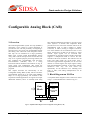
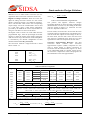
A simplified block diagram of the CAB can be found
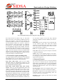
in fig. 2.1, and a detailed one is shown in fig. 2.2
Comparators
Gain
Block
Reference Block
Data
Conversion
Block
Output
Buffers
Fig 2.1: Simplified Block Diagram of the Configurable Analog Block (CAB)
Chapter 3. Configurable Analog Block (CAB)
2