1
SIDSA
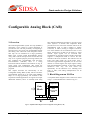
Channels configured as DACs convert the digital word
stored in the corresponding 8-bit register when
controlled by the µP. Channels used as ADCs, set up
their results when the conversion ends. The converted
data can be read in two ways:
• operating to Plselout(2:0) to obtain data through
Plout(7:0) to the programmable logic, or
• addressing the control registers mapped as memory
locations from the µP.
cmp
SAR
Regs.
DAC
IN
Figure 4.3. Successive approximation ADC loop
The beginning of the conversion can be independently
controlled for each channel. The process is depicted
below in table 4.3.
Cycle
1
2
3
4
5
6
7
8
9
10*
result of comparison
A
B
C
D
E
F
G
H
I
-
Semiconductor Design Solutions
Approximation
0111 1111
A011 1111
AB01 1111
ABC0 1111
ABCD 0111
ABCD E011
ABCD EF01
ABCD EFG0
ABCD EFGH
ABCD EFGH
* in continuous conversion mode, this cycle will begin a new
conversion, linking with cycle 1.
Table 4.3: Conversion sequence
When the conversion block is programmed with 9- or
10-bit ADC channels, the corresponding SARs form
groups (SAR#1 & SAR#2 and/or SAR#3 & SAR#4 to
obtain 9-bit ADCs or all of them to obtain a 10-bit
converter); when this occurs, the grouped SARs work
one or two cycles phased, respectively. At the end of
each conversion , SARs send their results to the In/Out
Registers and enable the interrupt generation block. On
continuous conversion modes that would start another
conversion.
During the conversion cycles the conversion command
for each chhanel could be independently issued either
from the programmable logic or the µP. This would
provoke a failure in the running conversion and the
following one. This would be critical in continuous
conversion modes because the error would be
propagated and could lead to unexpected results.
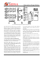
In/Out Registers Block: It consists of four 8-bit and
two 10-bit registers used to store the input or output
digital data from the data conversion block. The 10-bit
registers have read-only access and they are used to
store data in 4-multiplexed channels ADCs
configuration.
Chapter 3. Configurable Analog Block (CAB)
If the conversion block groups any channels to create a
9/10-bit converter, two registers will be needed. In
µP-controlled converters more significant bits must be
written first (see Table 4.4).
PLselout(3:0)
000 (dat1*)
001 (dat2*)
010 (dat3*)
011 (dat4*)
100 (dat5*)
101 (dat6*)
110 (dat7*)
111 (dat*8)
data
Ch#1 (7:0)
Ch#2 (7:0)
Ch#3 (7:0)
Ch#4 (7:0)
-
9-bit ch.+
Ch#A (7:0)
Ch#A (8:1)
Ch#B (7:0)
Ch#B (8:1)
-
10-bit ch +
Ch#A (7:0)
Ch#A (9:2)
Ch#B (7:0) **
Ch#B (9:2) **
Ch#C (7:0) **
Ch#C (9:2) **
Ch#D (7:0) **
Ch#D (9:2) **
* µP control registers (see section 2.4) when µP controlled
** only available in 4-mux channel 10-bit converter
+
PLoutExt(1:0) gives the 2 least significant bits of the channel
selected
(for
example,
if
PLselout(3:0)=’b011,
PLout=Ch#B(9:2) and PLoutExt(1:0)=Ch#B(1:0)).
Table 4.4: Conversion outputs
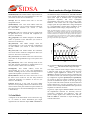
Interrupt Generation Block: This block provides the
end of conversion signals when at least one channel is
configured as ADC. It has independent protocols for
the µP and the Programmable Logic. Both protocols
work simultaneously (it allows different control for the
start and end of conversion).
When a channel reaches the end of the conversion, this
block acts as follows :
• a pulse is sent through the corresponding bit of
PLdone1-4,
• If the corresponding bit is not masked by
adc_enINT(3:0), an interrupt is sent to the µP
(signal ADC_int) and the conversion status in the
nibble mPdone(3:0) is updated. Both adc_INT and
mPdone(3:0) are reset when the µP reads the
nibble.
In 9/10-bit conversion modes only the corresponding
bit of the first channel grouped is used.
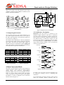
4.2 Configuration
The configuration of this block is controlled from the
µP. To program the conversion block, the µP must
access to the 64 bit memory and write the information
in the corresponding addresses (see Section 7).
Different configurations are listed below in table 4.5:
9