1
SIDSA
Semiconductor Design Solutions
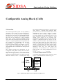
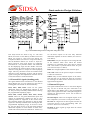
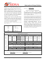
Fig. 3.1: Gain Block
The amplification channels of the Gain Block have a
power down feature which can be used to cut the
power supply for the selected cells. The three gain
stages of each channel share the same power down bit.
To set a complete channel in the power down mode,
the corresponding bit in configuration register
ONamp(3:0) must be reset to zero (ONamp(0)
corresponds to channel #1, ONamp(3) corresponds to
channel #4).
Note: When a gain stage is set to the power down mode, all bias
currents and input resistors are disconnected. Appropriate settling
times must be allowed upon subsequent power up.
3.1 Gain Stage
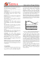
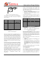
Fig. 3.3 qualitatively shows the structure of a gain
stage.
Note: In figures 3.3 and 3.4 the triangle represents a fully balanced
differential operational amplifier with infinte input impedance. It
does not symbolize a complete gain stage like in figures 2.2 and 3.1.
Different gains are obtained by modulating the input
resistance Rin . A gain select nibble gs(3:0) is used to
program the gain of the stage in linear steps from 0 to
15. The offset of the differential output signal can be
configured by injecting a differential current regulated
by an offset select byte off(7:0) in increasing discrete
values from -128 to 127. Each step correspond
approximately to a 1.5mV of differential voltage at the
output. Four extra bits CMRR(3:0) are used to
intendedly asymmetrize the two branches of the
differential system by slightly modulating only one of
the feedback branches with a small exra resistor RCMRR,
thus giving an extra degree of freedom to adjust the
CMRR, which greatly depends on the exact matching
of the two branches. The CMRR function should have
a minimum within the interval 0 to 15 of the
CMRR(3:0) nibble.
Note: It is not guaranteed the monotonicity nor a good linearity of
the offset control, so this feature should not be used to build an 8bit digital to analog converter (concrete specifications will be given
in the next version of this manual).
3.2 Direct Access to Operational Amplifiers
Fig. 3.3: Internal Structure of a Gain Stage
Chapter 3. Configurable Analog Block (CAB)
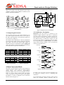
As depicted in fig. 3.3, each gain stage is based on a
fully balanced differential operational amplifier. It is
possible to directly access these cells by selecting the
direct mode, only available for channels #2 and #3. To
select the direct mode, bits Dir2N (for channel #2) or
Dir3N (for channel #3) must be reset to zero (they
have to be set to one for normal operation). In this
mode, pins In2P, In2N, Out2P and Out2N are the
direct inputs and outputs of a fully balanced differential
operational amplifier whose output is also connected to
the two remaining gain stages of channel #2 (In3P,
In3N, Out3P and Out3N can be used the same way in
channel #3). Fig. 3.4 presents channels #3 and #4 in the
6