1
SIDSA
Semiconductor Design Solutions
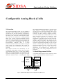
disabled so as to obtain linear conversion (see the
Application Notes section for non-linear conversion).
LS
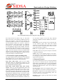
Digital to Analog Converters: Each one of the four
digital to analog converters consists of a 256 resistor
divider connected between two buffered references,
and a 8-bit decoder which selects the corresponding
output voltage. Two 8-bit cascaded DACs can be used
as a 9-bit DAC using a final analog multiplexer
governed by the MSB of the 9-bit word, and ditto for
using two 9-bit DACs to form a 10-bit block.
Vref
− Vref
P
N
256
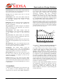
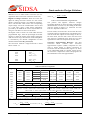
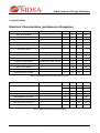
Table 4.1: Conversion table for a single 8-bit DAC
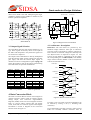
The positive and negative reference voltages
assignment depends on DACs grouping configuration
(described later in section 4.2). According to the labels
used for signals in Figure 4.2., references for each
DAC are depicted on Table 4.2.
In 9-bit modes, two 8-bit DACs are fed with the same
word (the eight less significant bits). The highest one is
used to select their outputs as final voltage. In the 10bit DAC mode, the four DACs share the same word
(the eight less signinficant bits) while the two most
significant bits select the output from the four DACs.
The digital word to convert can come either from the
programmable logic, from the µP through the In/Out
registers or from the output of the SARs (closing the
A/D conversion loop). The selection of this multiplexer
is controlled by the AD/DA configuration of each
channel and the nibble adc_source(3:0).
Successive Approximation Registers: The data
conversion
block
contains
four
successive
approximation registers (SARs) composed of 8 bits
used to obtain analog to digital conversions in
association with the internal DACs (Figure 4.4). There
is one independent SAR per channel, which receives
the successive comparisons results and programs the
associated DAC to the next approximation.
The conversion table for a single 8-bit DAC is listed
below in table 4.1:
Word
0x00
0x01
0x02
.....
0xFE
0xFF
=
where V
Output
VrefN
VrefN + VLS
VrefN + 2 VLS
VrefP - 2 VLS
VrefP - VLS
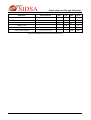
Table 4.2. Reference assignments
DAC #1
adc_group
VrefP
DAC #2
VrefN
VrefP
DAC #3
VrefN
DAC #4
VrefP
VrefN
VrefP
VrefN
Vref3
Vref4
Vref5
Vref4
00XX
Vref1
Vref2
Vref3
Vref2
0101
Vref1
Vref2
Vref3=Vref1
Vref2
Vref3=Vref1 Vref4=Vref2 Vref5=Vref1 Vref4=Vref2
0110
Vref1
Vref2
Vref3=Vref1
Vref2
Vref3=Vref1
Vref4
Vref5
Vref4
0111
Vref1
Vref2
Vref3=Vref1
Vref2
Vref3=Vref1
Vref4
Vref5=Vref3
Vref4
DAC #1234 → VrefP = Vref1, VrefN = Vref5. Vref2 = off, Vref3 = off, Vref4 = off.
1000
1001
Vref1
Vref2
Vref3
Vref2
1010
DAC #12 → VrefP = Vref1, VrefN = Vref3. Vref2 = off.
1011
DAC #12 → VrefP = Vref1, VrefN = Vref3. Vref2 = off.
Vref4
Vref3
Vref4
Vref5
DAC #34 → VrefP = Vref5, VrefN = Vref3. Vref4 = off.
DAC #1234 → VrefP = Vref1, VrefN = Vref5. Vref2 = off, Vref3 = off, Vref4 = off.
1100
DAC #12 → VrefP = Vref1, VrefN = Vref3. Vref2 = off.
1101
1110
Vref1
Vref2
Vref3=Vref1
Vref2
DAC #12 → VrefP = Vref1, VrefN = Vref3. Vref2 = off.
1111
Notes :
DAC #34 → VrefP = Vref3, VrefN = Vref5. Vref4 = off.
Vref4
Vref3
Vref4
Vref5=Vref3
DAC #34 → VrefP = Vref3, VrefN = Vref5. Vref4 = off.
DAC #34 → VrefP=Vref5=Vref1,VrefN=Vref3. Vref4=off.
a) 9/10-bit DACs are referred to as group of the number of the channels used
b) `off´ represents that buffer must be disabled to obtain a constant VLS (see Applications Notes).
c)
V
LS
=
Vref
− Vref
Vref − Vref
P
N
P
N
in 9-bits DACs ; and, V
=
in 10-bit DAC
512
LS
1024
Chapter 3. Configurable Analog Block (CAB)
8