1
Datasheet
RL78/G13
R01DS0131EJ0310
Rev.3.10
Nov 15, 2013
RENESAS MCU
True Low Power Platform (as low as 66 µA/MHz, and 0.57 µA for RTC + LVD), 1.6 V to 5.5 V
operation, 16 to 512 Kbyte Flash, 41 DMIPS at 32 MHz, for General Purpose Applications
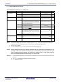
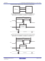
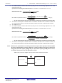
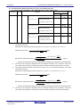
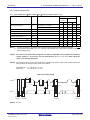
1. OUTLINE
1.1 Features
Ultra-Low Power Technology
• 1.6 V to 5.5 V operation from a single supply
• Stop (RAM retained): 0.23 µA, (LVD enabled): 0.31
µA
• Halt (RTC + LVD): 0.57 µA
• Snooze: 0.70 mA (UART), 1.20 mA (ADC)
• Operating: 66 µA/MHz
16-bit RL78 CPU Core
• Delivers 41 DMIPS at maximum operating frequency
of 32 MHz
• Instruction Execution: 86% of instructions can be
executed in 1 to 2 clock cycles
• CISC Architecture (Harvard) with 3-stage pipeline
• Multiply Signed & Unsigned: 16 x 16 to 32-bit result in
1 clock cycle
• MAC: 16 x 16 to 32-bit result in 2 clock cycles
• 16-bit barrel shifter for shift & rotate in 1 clock cycle
• 1-wire on-chip debug function
Main Flash Memory
• Density: 16 KB to 512 KB
• Block size: 1 KB
• On-chip single voltage flash memory with protection
from block erase/writing
• Self-programming with secure boot swap function
and flash shield window function
Data Flash Memory
• Data Flash with background operation
• Data flash size: 4 KB to 8 KB size options
• Erase Cycles: 1 Million (typ.)
• Erase/programming voltage: 1.8 V to 5.5 V
RAM
• 2 KB to 32 KB size options
• Supports operands or instructions
• Back-up retention in all modes
High-speed On-chip Oscillator
• 32 MHz with +/− 1% accuracy over voltage (1.8 V to
5.5 V) and temperature (−20 °C to 85 °C)
• Pre-configured settings: 32 MHz, 24 MHz, 16 MHz,
12 MHz, 8 MHz, 6 MHz, 4 MHz, 3 MHz, 2 MHz,
and 1 MHz
Reset and Supply Management
• Power-on reset (POR) monitor/generator
• Low voltage detection (LVD) with 14 setting options
(Interrupt and/or reset function)
R01DS0131EJ0310 Rev.3.10
Nov 15, 2013
Data Memory Access (DMA) Controller
• Up to 4 fully programmable channels
• Transfer unit: 8- or 16-bit
Multiple Communication Interfaces
2
• Up to 8 x I C master
2
• Up to 2 x I C multi-master
• Up to 8 x CSI/SPI (7-, 8-bit)
• Up to 4 x UART (7-, 8-, 9-bit)
• Up to 1 x LIN
Extended-Function Timers
• Multi-function 16-bit timers: Up to 16 channels
• Real-time clock (RTC): 1 channel (full calendar and
alarm function with watch correction function)
• Interval Timer: 12-bit, 1 channel
• 15 kHz watchdog timer : 1 channel (window function)
Rich Analog
• ADC: Up to 26 channels, 10-bit resolution, 2.1 µs
conversion time
• Supports 1.6 V
• Internal voltage reference (1.45 V)
• On-chip temperature sensor
Safety Features (IEC or UL 60730 compliance)
• Flash memory CRC calculation
• RAM parity error check
• RAM write protection
• SFR write protection
• Illegal memory access detection
• Clock stop/ frequency detection
• ADC self-test
General Purpose I/O
• 5V tolerant, high-current (up to 20 mA per pin)
• Open-Drain, Internal Pull-up support
• Different potential interface support: Can connect to
a 1.8/2.5/3 V device
Operating Ambient Temperature
• Standard: −40 °C to +85 °C
• Extended: −40 °C to +105 °C
Package Type and Pin Count
From 3mm x 3mm to 14mm x 20mm
QFP: 44, 48, 52, 64, 80, 100, 128
QFN: 24, 32, 40, 48
SSOP: 20, 30
LGA: 25, 36
BGA: 64
Page 1 of 194
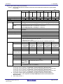
RL78/G13
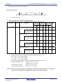
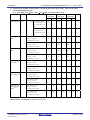
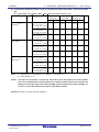
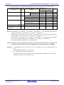
1. OUTLINE
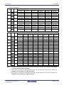
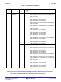
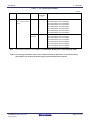
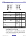
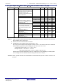
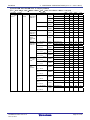
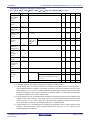
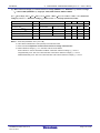
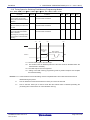
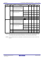
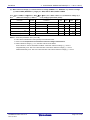
ROM, RAM capacities
Flash
Data
RAM
RL78/G13
ROM
flash
128
KB
8 KB
96
KB
8 KB
64
KB
4 KB
4 KB
R5F1006E
R5F1007E
R5F1008E
R5F100AE
R5F100BE
R5F100CE
−
Note 1
R5F1016E
R5F1017E
R5F1018E
R5F101AE
R5F101BE
R5F101CE
48
KB
4 KB
3 KB
R5F1006D
R5F1007D
R5F1008D
R5F100AD
R5F100BD
R5F100CD
R5F1016D
R5F1017D
R5F1018D
R5F101AD
R5F101BD
R5F101CD
32
KB
4 KB
R5F1006C
R5F1007C
R5F1008C
R5F100AC
R5F100BC
R5F100CC
R5F1016C
R5F1017C
R5F1018C
R5F101AC
R5F101BC
R5F101CC
16
KB
4 KB
R5F1006A
R5F1007A
R5F1008A
R5F100AA
R5F100BA
R5F100CA
R5F1016A
R5F1017A
R5F1018A
R5F101AA
R5F101BA
R5F101CA
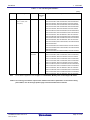
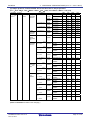
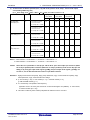
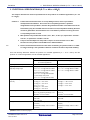
Flash
Data
ROM
flash
512
KB
8 KB
384
KB
8 KB
256
KB
8 KB
192
KB
8 KB
128
KB
8 KB
96
KB
8 KB
64
KB
4 KB
48
KB
4 KB
32
KB
4 KB
16
KB
4 KB
20 pins
24 pins
25 pins
30 pins
32 pins
36 pins
−
−
−
R5F100AG
R5F100BG
R5F100CG
−
−
−
R5F101AG
R5F101BG
R5F101CG
−
−
−
R5F100AF
R5F100BF
R5F100CF
−
−
−
R5F101AF
R5F101BF
R5F101CF
12 KB
−
8 KB
−
−
2 KB
−
2 KB
−
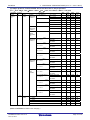
RAM
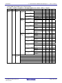
RL78/G13
40 pins
44 pins
48 pins
52 pins
64 pins
80 pins
100 pins
128 pins
−
R5F100FL
R5F100GL
R5F100JL
R5F100LL
R5F100ML
R5F100PL
R5F100SL
−
R5F101FL
R5F101GL
R5F101JL
R5F101LL
R5F101ML
R5F101PL
R5F101SL
−
R5F100FK
R5F100GK
R5F100JK
R5F100LK
R5F100MK R5F100PK
R5F100SK
−
R5F101FK
R5F101GK
R5F101JK
R5F101LK
R5F101MK R5F101PK
R5F101SK
−
R5F100FJ
R5F100GJ
R5F100JJ
R5F100LJ
R5F100MJ
R5F100PJ
R5F100SJ
R5F101FJ
R5F101MJ
32 KB
Note 3
−
24 KB
−
−
20 KB
Note 2
16 KB
−
R5F101JJ
R5F101LJ
R5F101PJ
R5F101SJ
R5F100JH
R5F100LH R5F100MH R5F100PH
R5F100SH
R5F101EH
R5F101FH R5F101GH
R5F101JH
R5F101LH R5F101MH R5F101PH
R5F101SH
R5F100EG R5F100FG R5F100GG R5F100JG
R5F100LG R5F100MG R5F100PG
−
R5F101LG R5F101MG R5F101PG
−
8 KB
R5F100EF
R5F100LF
R5F100MF
R5F100PF
−
R5F101EF
R5F101FF
R5F101GF
R5F101JF
R5F101LF
R5F101MF
R5F101PF
−
4 KB
R5F100EE
R5F100FE
R5F100GE
R5F100JE
R5F100LE
−
−
−
−
R5F100FF
R5F100GF
R5F100JF
Note 1
3 KB
−
2 KB
−
−
R5F101GJ
R5F100FH R5F100GH
R5F101EG R5F101FG R5F101GG R5F101JG
12 KB
−
−
−
R5F100EH
2 KB
R5F101EE
R5F101FE
R5F101GE
R5F101JE
R5F101LE
−
−
−
R5F100ED
R5F100FD R5F100GD
R5F100JD
R5F100LD
−
−
−
R5F101ED
R5F101FD R5F101GD
R5F101JD
R5F101LD
−
−
−
R5F100EC
R5F100FC R5F100GC
R5F100JC
R5F100LC
−
−
−
R5F101EC
R5F101FC R5F101GC
R5F101JC
R5F101LC
−
−
−
R5F100EA
R5F100FA
R5F100GA
−
−
−
−
−
R5F101EA
R5F101FA
R5F101GA
−
−
−
−
−
Notes 1. This is about 3 KB when the self-programming function and data flash function are used. (For details, see CHAPTER
3 in the RL78/G13 User’s Manual Hardware)
2. This is about 19 KB when the self-programming function and data flash function are used. (For details, see
CHAPTER 3 in the RL78/G13 User’s Manual Hardware)
3. This is about 31 KB when the self-programming function and data flash function are used. (For details, see
CHAPTER 3 in the RL78/G13 User’s Manual Hardware)
R01DS0131EJ0310 Rev.3.10
Nov 15, 2013
Page 2 of 194
RL78/G13
1. OUTLINE
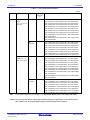
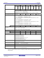
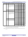
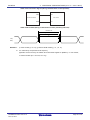
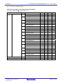
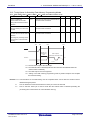
1.2 List of Part Numbers
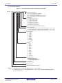
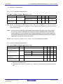
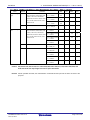
Figure 1-1. Part Number, Memory Size, and Package of RL78/G13
Part No. R 5 F 1 0 0 L E A x x x F B #V0
Packaging specification
#U0
#V0
#W0
#X0
: Tray (HWQFN,VFBGA,WFLGA)
: Tray (LFQFP,LQFP,LSSOP)
: Embossed Tape (HWQFN,VFBGA,WFLGA)
: Embossed Tape (LFQFP, LQFP, LSSOP)
Package type:
SP: LSSOP, 0.65 mm pitch
FP : LFQFP, 0.80 mm pitch
FA : LFQFP, 0.65 mm pitch
FB : LFQFP, 0.50 mm pitch
NA : HWQFN, 0.50 mm pitch
LA : WFLGA, 0.50 mm pitch Note 1
BG : VFBGA, 0.40 mm pitch Note 1
ROM number (Omitted with blank products)
Fields of application:
A : Consumer applications, operating ambient temperature : -40˚C to +85˚C
D : Industrial applications, operating ambient temperature : -40˚C to +85˚C
G : Industrial applications, operating ambient temperature : -40˚C to +105˚C
ROM capacity:
A : 16 KB
C : 32 KB
D : 48 KB
E : 64 KB
F : 96 KB
G : 128 KB
H : 192 KB
J : 256 KB
K : 384 KB Note 2
L : 512 KBNote 2
Pin count:
6 : 20-pin
7 : 24-pin
8 : 25-pin Note 1
A : 30-pin
B : 32-pin
C : 36-pin Note 1
E : 40-pin
F : 44-pin
G : 48-pin
J : 52-pin
L : 64-pin
M : 80-pin
P : 100-pin
S : 128-pin Note 2
RL78/G13 group
Note 2
Memory type:
F : Flash memory
Renesas MCU
Renesas semiconductor product
Notes
1. Products only for “A: Consumer applications (TA = −40 to +85°C)”
2. Products only for “A: Consumer applications (TA = −40 to +85°C)”, and ” D: Industrial applications
(TA = −40 to +85°C)
R01DS0131EJ0310 Rev.3.10
Nov 15, 2013
Page 3 of 194
RL78/G13
1. OUTLINE
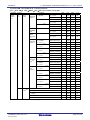
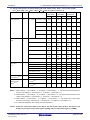
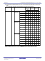
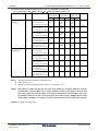
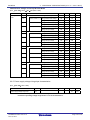
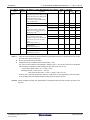
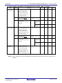
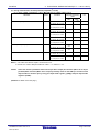
Table 1-1. List of Ordering Part Numbers
(1/12)
Pin
Package
count
Data
Fields of
flash
Application
Ordering Part Number
Note
20 pins
20-pin plastic LSSOP
Mounted
A
R5F1006AASP#V0, R5F1006CASP#V0, R5F1006DASP#V0,
(7.62 mm (300), 0.65
R5F1006EASP#V0
mm pitch)
R5F1006AASP#X0, R5F1006CASP#X0, R5F1006DASP#X0,
R5F1006EASP#X0
D
R5F1006ADSP#V0, R5F1006CDSP#V0, R5F1006DDSP#V0,
R5F1006EDSP#V0
R5F1006ADSP#X0, R5F1006CDSP#X0, R5F1006DDSP#X0,
R5F1006EDSP#X0
G
R5F1006AGSP#V0, R5F1006CGSP#V0, R5F1006DGSP#V0,
R5F1006EGSP#V0
R5F1006AGSP#X0, R5F1006CGSP#X0, R5F1006DGSP#X0,
R5F1006EGSP#X0
Not
A
mounted
R5F1016AASP#V0, R5F1016CASP#V0, R5F1016DASP#V0,
R5F1016EASP#V0
R5F1016AASP#X0, R5F1016CASP#X0, R5F1016DASP#X0,
R5F1016EASP#X0
D
R5F1016ADSP#V0, R5F1016CDSP#V0, R5F1016DDSP#V0,
R5F1016EDSP#V0
R5F1016ADSP#X0, R5F1016CDSP#X0, R5F1016DDSP#X0,
R5F1016EDSP#X0
24 pins
24-pin plastic
Mounted
A
R5F1007AANA#U0, R5F1007CANA#U0, R5F1007DANA#U0,
HWQFN (4 × 4mm,
R5F1007EANA#U0
0.5 mm pitch)
R5F1007AANA#W0, R5F1007CANA#W0, R5F1007DANA#W0,
R5F1007EANA#W0
D
R5F1007ADNA#U0, R5F1007CDNA#U0, R5F1007DDNA#U0,
R5F1007EDNA#U0
R5F1007ADNA#W0, R5F1007CDNA#W0, R5F1007DDNA#W0,
R5F1007EDNA#W0
G
R5F1007AGNA#U0, R5F1007CGNA#U0, R5F1007DGNA#U0,
R5F1007EGNA#U0
R5F1007AGNA#W0, R5F1007CGNA#W0, R5F1007DGNA#W0,
R5F1007EGNA#W0
Not
A
mounted
R5F1017AANA#U0, R5F1017CANA#U0, R5F1017DANA#U0,
R5F1017EANA#U0
R5F1017AANA#W0, R5F1017CANA#W0, R5F1017DANA#W0,
R5F1017EANA#W0
D
R5F1017ADNA#U0, R5F1017CDNA#U0, R5F1017DDNA#U0,
R5F1017EDNA#U0
R5F1017ADNA#W0, R5F1017CDNA#W0, R5F1017DDNA#W0,
R5F1017EDNA#W0
Note
For the fields of application, refer to Figure 1-1 Part Number, Memory Size, and Package of RL78/G13.
Caution The ordering part numbers represent the numbers at the time of publication. For the latest ordering
part numbers, refer to the target product page of the Renesas Electronics website.
R01DS0131EJ0310 Rev.3.10
Nov 15, 2013
Page 4 of 194
RL78/G13
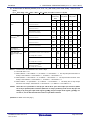
1. OUTLINE
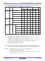
Table 1-1. List of Ordering Part Numbers
(2/12)
Pin
count
Package
Data
flash
Fields of
Application
Ordering Part Number
Note
25 pins
25-pin plastic
WFLGA (3 × 3 mm,
Mounted
A
Not
mounted
A
Mounted
A
0.5 mm pitch)
30 pins
30-pin plastic LSSOP
(7.62 mm (300), 0.65
mm pitch)
D
G
Not
mounted
A
D
32 pins
32-pin plastic
HWQFN (5 × 5 mm,
Mounted
A
0.5 mm pitch)
D
G
Not
mounted
A
D
Note
R5F1008AALA#U0, R5F1008CALA#U0, R5F1008DALA#U0,
R5F1008EALA#U0
R5F1008AALA#W0, R5F1008CALA#W0, R5F1008DALA#W0,
R5F1008EALA#W0
R5F1018AALA#U0, R5F1018CALA#U0, R5F1018DALA#U0,
R5F1018EALA#U0
R5F1018AALA#W0, R5F1018CALA#W0, R5F1018DALA#W0,
R5F1018EALA#W0
R5F100AAASP#V0, R5F100ACASP#V0, R5F100ADASP#V0,
R5F100AEASP#V0, R5F100AFASP#V0, R5F100AGASP#V0
R5F100AAASP#X0, R5F100ACASP#X0, R5F100ADASP#X0
R5F100AEASP#X0, R5F100AFASP#X0, R5F100AGASP#X0
R5F100AADSP#V0, R5F100ACDSP#V0, R5F100ADDSP#V0,
R5F100AEDSP#V0, R5F100AFDSP#V0, R5F100AGDSP#V0
R5F100AADSP#X0, R5F100ACDSP#X0, R5F100ADDSP#X0,
R5F100AEDSP#X0, R5F100AFDSP#X0, R5F100AGDSP#X0
R5F100AAGSP#V0, R5F100ACGSP#V0,
R5F100ADGSP#V0,R5F100AEGSP#V0,
R5F100AFGSP#V0, R5F100AGGSP#V0
R5F100AAGSP#X0, R5F100ACGSP#X0,
R5F100ADGSP#X0,R5F100AEGSP#X0,
R5F100AFGSP#X0, R5F100AGGSP#X0
R5F101AAASP#V0, R5F101ACASP#V0, R5F101ADASP#V0,
R5F101AEASP#V0, R5F101AFASP#V0, R5F101AGASP#V0
R5F101AAASP#X0, R5F101ACASP#X0, R5F101ADASP#X0,
R5F101AEASP#X0, R5F101AFASP#X0, R5F101AGASP#X0
R5F101AADSP#V0, R5F101ACDSP#V0, R5F101ADDSP#V0,
R5F101AEDSP#V0, R5F101AFDSP#V0, R5F101AGDSP#V0
R5F101AADSP#X0, R5F101ACDSP#X0, R5F101ADDSP#X0,
R5F101AEDSP#X0, R5F101AFDSP#X0, R5F101AGDSP#X0
R5F100BAANA#U0, R5F100BCANA#U0, R5F100BDANA#U0,
R5F100BEANA#U0, R5F100BFANA#U0, R5F100BGANA#U0
R5F100BAANA#W0, R5F100BCANA#W0, R5F100BDANA#W0,
R5F100BEANA#W0, R5F100BFANA#W0, R5F100BGANA#W0
R5F100BADNA#U0, R5F100BCDNA#U0, R5F100BDDNA#U0,
R5F100BEDNA#U0, R5F100BFDNA#U0, R5F100BGDNA#U0
R5F100BADNA#W0, R5F100BCDNA#W0, R5F100BDDNA#W0,
R5F100BEDNA#W0, R5F100BFDNA#W0, R5F100BGDNA#W0
R5F100BAGNA#U0, R5F100BCGNA#U0, R5F100BDGNA#U0,
R5F100BEGNA#U0, R5F100BFGNA#U0, R5F100BGGNA#U0
R5F100BAGNA#W0, R5F100BCGNA#W0, R5F100BDGNA#W0,
R5F100BEGNA#W0, R5F100BFGNA#W0, R5F100BGGNA#W0
R5F101BAANA#U0, R5F101BCANA#U0, R5F101BDANA#U0,
R5F101BEANA#U0, R5F101BFANA#U0, R5F101BGANA#U0
R5F101BAANA#W0, R5F101BCANA#W0, R5F101BDANA#W0,
R5F101BEANA#W0, R5F101BFANA#W0, R5F101BGANA#W0
R5F101BADNA#U0, R5F101BCDNA#U0, R5F101BDDNA#U0,
R5F101BEDNA#U0, R5F101BFDNA#U0, R5F101BGDNA#U0
R5F101BADNA#W0, R5F101BCDNA#W0, R5F101BDDNA#W0,
R5F101BEDNA#W0, R5F101BFDNA#W0, R5F101BGDNA#W0
For the fields of application, refer to Figure 1-1 Part Number, Memory Size, and Package of RL78/G13.
Caution The ordering part numbers represent the numbers at the time of publication. For the latest ordering
part numbers, refer to the target product page of the Renesas Electronics website.
R01DS0131EJ0310 Rev.3.10
Nov 15, 2013
Page 5 of 194
RL78/G13
1. OUTLINE
Table 1-1. List of Ordering Part Numbers
(3/12)
Pin
Package
count
Data
Fields of
flash
Application
Ordering Part Number
Note
36 pins
36-pin plastic WFLGA
(4 × 4 mm, 0.5 mm
Mounted
A
R5F100CAALA#U0, R5F100CCALA#U0, R5F100CDALA#U0,
R5F100CEALA#U0, R5F100CFALA#U0, R5F100CGALA#U0
R5F100CAALA#W0, R5F100CCALA#W0, R5F100CDALA#W0,
R5F100CEALA#W0, R5F100CFALA#W0, R5F100CGALA#W0
Not
mounted
A
R5F101CAALA#U0, R5F101CCALA#U0, R5F101CDALA#U0,
R5F101CEALA#U0, R5F101CFALA#U0, R5F101CGALA#U0
R5F101CAALA#W0, R5F101CCALA#W0, R5F101CDALA#W0,
R5F101CEALA#W0, R5F101CFALA#W0, R5F101CGALA#W0
Mounted
A
R5F100EAANA#U0, R5F100ECANA#U0, R5F100EDANA#U0,
pitch)
40 pins
40-pin plastic HWQFN
(6 × 6 mm, 0.5 mm
R5F100EEANA#U0, R5F100EFANA#U0, R5F100EGANA#U0,
pitch)
R5F100EHANA#U0
R5F100EAANA#W0, R5F100ECANA#W0, R5F100EDANA#W0,
R5F100EEANA#W0, R5F100EFANA#W0, R5F100EGANA#W0,
R5F100EHANA#W0
D
R5F100EADNA#U0, R5F100ECDNA#U0, R5F100EDDNA#U0,
R5F100EEDNA#U0, R5F100EFDNA#U0, R5F100EGDNA#U0,
R5F100EHDNA#U0
R5F100EADNA#W0, R5F100ECDNA#W0, R5F100EDDNA#W0,
R5F100EEDNA#W0, R5F100EFDNA#W0, R5F100EGDNA#W0,
R5F100EHDNA#W0
G
R5F100EAGNA#U0, R5F100ECGNA#U0, R5F100EDGNA#U0,
R5F100EEGNA#U0, R5F100EFGNA#U0, R5F100EGGNA#U0,
R5F100EHGNA#U0
R5F100EAGNA#W0, R5F100ECGNA#W0,
R5F100EDGNA#W0, R5F100EEGNA#W0, R5F100EFGNA#W0,
R5F100EGGNA#W0, R5F100EHGNA#W0
Not
A
mounted
R5F101EAANA#U0, R5F101ECANA#U0, R5F101EDANA#U0,
R5F101EEANA#U0, R5F101EFANA#U0, R5F101EGANA#U0,
R5F101EHANA#U0
R5F101EAANA#W0, R5F101ECANA#W0, R5F101EDANA#W0,
R5F101EEANA#W0, R5F101EFANA#W0, R5F101EGANA#W0,
R5F101EHANA#W0
D
R5F101EADNA#U0, R5F101ECDNA#U0, R5F101EDDNA#U0,
R5F101EEDNA#U0, R5F101EFDNA#U0, R5F101EGDNA#U0,
R5F101EHDNA#U0
R5F101EADNA#W0, R5F101ECDNA#W0, R5F101EDDNA#W0,
R5F101EEDNA#W0, R5F101EFDNA#W0, R5F101EGDNA#W0,
R5F101EHDNA#W0
Note
For the fields of application, refer to Figure 1-1 Part Number, Memory Size, and Package of RL78/G13.
Caution The ordering part numbers represent the numbers at the time of publication. For the latest ordering
part numbers, refer to the target product page of the Renesas Electronics website.
R01DS0131EJ0310 Rev.3.10
Nov 15, 2013
Page 6 of 194
RL78/G13
1. OUTLINE
Table 1-1. List of Ordering Part Numbers
(4/12)
Pin
Package
Data flash
count
Ordering Part Number
Fields of
Application
Note
44 pins
44-pin plastic LQFP
Mounted
A
R5F100FAAFP#V0, R5F100FCAFP#V0, R5F100FDAFP#V0,
(10 × 10 mm, 0.8
R5F100FEAFP#V0, R5F100FFAFP#V0, R5F100FGAFP#V0,
mm pitch)
R5F100FHAFP#V0, R5F100FJAFP#V0, R5F100FKAFP#V0,
R5F100FLAFP#V0
R5F100FAAFP#X0, R5F100FCAFP#X0, R5F100FDAFP#X0,
R5F100FEAFP#X0, R5F100FFAFP#X0, R5F100FGAFP#X0,
R5F100FHAFP#X0, R5F100FJAFP#X0, R5F100FKAFP#X0,
R5F100FLAFP#X0
D
R5F100FADFP#V0, R5F100FCDFP#V0, R5F100FDDFP#V0,
R5F100FEDFP#V0, R5F100FFDFP#V0, R5F100FGDFP#V0,
R5F100FHDFP#V0, R5F100FJDFP#V0, R5F100FKDFP#V0,
R5F100FLDFP#V0
R5F100FADFP#X0, R5F100FCDFP#X0, R5F100FDDFP#X0,
R5F100FEDFP#X0, R5F100FFDFP#X0, R5F100FGDFP#X0,
R5F100FHDFP#X0, R5F100FJDFP#X0, R5F100FKDFP#X0,
R5F100FLDFP#X0
G
R5F100FAGFP#V0, R5F100FCGFP#V0, R5F100FDGFP#V0,
R5F100FEGFP#V0, R5F100FFGFP#V0, R5F100FGGFP#V0,
R5F100FHGFP#V0, R5F100FJGFP#V0
R5F100FAGFP#X0, R5F100FCGFP#X0, R5F100FDGFP#X0,
R5F100FEGFP#X0, R5F100FFGFP#X0, R5F100FGGFP#X0,
R5F100FHGFP#X0, R5F100FJGFP#X0
Not
A
mounted
R5F101FAAFP#V0, R5F101FCAFP#V0, R5F101FDAFP#V0,
R5F101FEAFP#V0, R5F101FFAFP#V0, R5F101FGAFP#V0,
R5F101FHAFP#V0, R5F101FJAFP#V0, R5F101FKAFP#V0,
R5F101FLAFP#V0
R5F101FAAFP#X0, R5F101FCAFP#X0, R5F101FDAFP#X0,
R5F101FEAFP#X0, R5F101FFAFP#X0, R5F101FGAFP#X0,
R5F101FHAFP#X0, R5F101FJAFP#X0, R5F101FKAFP#X0,
R5F101FLAFP#X0
D
R5F101FADFP#V0, R5F101FCDFP#V0, R5F101FDDFP#V0,
R5F101FEDFP#V0, R5F101FFDFP#V0, R5F101FGDFP#V0,
R5F101FHDFP#V0, R5F101FJDFP#V0, R5F101FKDFP#V0,
R5F101FLDFP#V0
R5F101FADFP#X0, R5F101FCDFP#X0, R5F101FDDFP#X0,
R5F101FEDFP#X0, R5F101FFDFP#X0, R5F101FGDFP#X0,
R5F101FHDFP#X0, R5F101FJDFP#X0, R5F101FKDFP#X0,
R5F101FLDFP#X0
Note
For the fields of application, refer to Figure 1-1 Part Number, Memory Size, and Package of RL78/G13.
Caution The ordering part numbers represent the numbers at the time of publication. For the latest ordering
part numbers, refer to the target product page of the Renesas Electronics website.
R01DS0131EJ0310 Rev.3.10
Nov 15, 2013
Page 7 of 194
RL78/G13
1. OUTLINE
Table 1-1. List of Ordering Part Numbers
(5/12)
Pin count
Package
Data flash
Ordering Part Number
Fields of
Application
Note
48 pins
48-pin plastic LFQFP
Mounted
A
R5F100GAAFB#V0, R5F100GCAFB#V0, R5F100GDAFB#V0,
(7 × 7 mm, 0.5 mm
R5F100GEAFB#V0, R5F100GFAFB#V0, R5F100GGAFB#V0,
pitch)
R5F100GHAFB#V0, R5F100GJAFB#V0, R5F100GKAFB#V0,
R5F100GLAFB#V0
R5F100GAAFB#X0, R5F100GCAFB#X0, R5F100GDAFB#X0,
R5F100GEAFB#X0, R5F100GFAFB#X0, R5F100GGAFB#X0,
R5F100GHAFB#X0, R5F100GJAFB#X0, R5F100GKAFB#X0,
R5F100GLAFB#X0
D
R5F100GADFB#V0, R5F100GCDFB#V0, R5F100GDDFB#V0,
R5F100GEDFB#V0, R5F100GFDFB#V0, R5F100GGDFB#V0,
R5F100GHDFB#V0, R5F100GJDFB#V0, R5F100GKDFB#V0,
R5F100GLDFB#V0
R5F100GADFB#X0, R5F100GCDFB#X0, R5F100GDDFB#X0,
R5F100GEDFB#X0, R5F100GFDFB#X0, R5F100GGDFB#X0,
R5F100GHDFB#X0, R5F100GJDFB#X0, R5F100GKDFB#X0,
R5F100GLDFB#X0
G
R5F100GAGFB#V0, R5F100GCGFB#V0,
R5F100GDGFB#V0, R5F100GEGFB#V0,
R5F100GFGFB#V0, R5F100GGGFB#V0,
R5F100GHGFB#V0, R5F100GJGFB#V0
R5F100GAGFB#X0, R5F100GCGFB#X0,
R5F100GDGFB#X0, R5F100GEGFB#X0,
R5F100GFGFB#X0, R5F100GGGFB#X0,
R5F100GHGFB#X0, R5F100GJGFB#X0
Not
A
mounted
R5F101GAAFB#V0, R5F101GCAFB#V0, R5F101GDAFB#V0,
R5F101GEAFB#V0, R5F101GFAFB#V0, R5F101GGAFB#V0,
R5F101GHAFB#V0, R5F101GJAFB#V0, R5F101GKAFB#V0,
R5F101GLAFB#V0
R5F101GAAFB#X0, R5F101GCAFB#X0, R5F101GDAFB#X0,
R5F101GEAFB#X0, R5F101GFAFB#X0, R5F101GGAFB#X0,
R5F101GHAFB#X0, R5F101GJAFB#X0, R5F101GKAFB#X0,
R5F101GLAFB#X0
D
R5F101GADFB#V0, R5F101GCDFB#V0, R5F101GDDFB#V0,
R5F101GEDFB#V0, R5F101GFDFB#V0, R5F101GGDFB#V0,
R5F101GHDFB#V0, R5F101GJDFB#V0, R5F101GKDFB#V0,
R5F101GLDFB#V0
R5F101GADFB#X0, R5F101GCDFB#X0, R5F101GDDFB#X0,
R5F101GEDFB#X0, R5F101GFDFB#X0, R5F101GGDFB#X0,
R5F101GHDFB#X0, R5F101GJDFB#X0, R5F101GKDFB#X0,
R5F101GLDFB#X0
Note
For the fields of application, refer to Figure 1-1 Part Number, Memory Size, and Package of RL78/G13.
Caution The ordering part numbers represent the numbers at the time of publication. For the latest ordering
part numbers, refer to the target product page of the Renesas Electronics website.
R01DS0131EJ0310 Rev.3.10
Nov 15, 2013
Page 8 of 194
RL78/G13
1. OUTLINE
Table 1-1. List of Ordering Part Numbers
(6/12)
Pin count
Package
Data flash
Ordering Part Number
Fields of
Application
Note
48 pins
48-pin plastic
Mounted
A
R5F100GAANA#U0, R5F100GCANA#U0, R5F100GDANA#U0,
HWQFN (7 × 7
R5F100GEANA#U0, R5F100GFANA#U0, R5F100GGANA#U0,
mm, 0.5 mm pitch)
R5F100GHANA#U0, R5F100GJANA#U0, R5F100GKANA#U0,
R5F100GLANA#U0
R5F100GAANA#W0, R5F100GCANA#W0,
R5F100GDANA#W0, R5F100GEANA#W0,
R5F100GFANA#W0, R5F100GGANA#W0,
R5F100GHANA#W0, R5F100GJANA#W0, R5F100GKANA#W0,
R5F100GLANA#W0
D
R5F100GADNA#U0, R5F100GCDNA#U0, R5F100GDDNA#U0,
R5F100GEDNA#U0, R5F100GFDNA#U0, R5F100GGDNA#U0,
R5F100GHDNA#U0, R5F100GJDNA#U0, R5F100GKDNA#U0,
R5F100GLDNA#U0
R5F100GADNA#W0, R5F100GCDNA#W0,
R5F100GDDNA#W0, R5F100GEDNA#W0,
R5F100GFDNA#W0, R5F100GGDNA#W0,
R5F100GHDNA#W0, R5F100GJDNA#W0,
R5F100GKDNA#W0, R5F100GLDNA#W0
G
R5F100GAGNA#U0, R5F100GCGNA#U0, R5F100GDGNA#U0,
R5F100GEGNA#U0, R5F100GFGNA#U0, R5F100GGGNA#U0,
R5F100GHGNA#U0, R5F100GJGNA#U0
R5F100GAGNA#W0, R5F100GCGNA#W0,
R5F100GDGNA#W0, R5F100GEGNA#W0,
R5F100GFGNA#W0, R5F100GGGNA#W0,
R5F100GHGNA#W0, R5F100GJGNA#W0
Not
A
mounted
R5F101GAANA#U0, R5F101GCANA#U0, R5F101GDANA#U0,
R5F101GEANA#U0, R5F101GFANA#U0, R5F101GGANA#U0,
R5F101GHANA#U0, R5F101GJANA#U0, R5F101GKANA#U0,
R5F101GLANA#U0
R5F101GAANA#W0, R5F101GCANA#W0,
R5F101GDANA#W0, R5F101GEANA#W0,
R5F101GFANA#W0, R5F101GGANA#W0,
R5F101GHANA#W0, R5F101GJANA#W0, R5F101GKANA#W0,
R5F101GLANA#W0
D
R5F101GADNA#U0, R5F101GCDNA#U0, R5F101GDDNA#U0,
R5F101GEDNA#U0, R5F101GFDNA#U0, R5F101GGDNA#U0,
R5F101GHDNA#U0, R5F101GJDNA#U0, R5F101GKDNA#U0,
R5F101GLDNA#U0
R5F101GADNA#W0, R5F101GCDNA#W0,
R5F101GDDNA#W0, R5F101GEDNA#W0,
R5F101GFDNA#W0, R5F101GGDNA#W0,
R5F101GHDNA#W0, R5F101GJDNA#W0,
R5F101GKDNA#W0, R5F101GLDNA#W0
Note
For the fields of application, refer to Figure 1-1 Part Number, Memory Size, and Package of RL78/G13.
Caution The ordering part numbers represent the numbers at the time of publication. For the latest ordering
part numbers, refer to the target product page of the Renesas Electronics website.
R01DS0131EJ0310 Rev.3.10
Nov 15, 2013
Page 9 of 194
RL78/G13
1. OUTLINE
Table 1-1. List of Ordering Part Numbers
(7/12)
Pin
Package
Data flash
Ordering Part Number
Fields of
count
Application
Note
52 pins
52-pin plastic LQFP
Mounted
A
R5F100JCAFA#V0, R5F100JDAFA#V0, R5F100JEAFA#V0,
(10 × 10 mm, 0.65
R5F100JFAFA#V0, R5F100JGAFA#V0, R5F100JHAFA#V0,
mm pitch)
R5F100JJAFA#V0, R5F100JKAFA#V0, R5F100JLAFA#V0
R5F100JCAFA#X0, R5F100JDAFA#X0, R5F100JEAFA#X0,
R5F100JFAFA#X0, R5F100JGAFA#X0, R5F100JHAFA#X0,
R5F100JJAFA#X0, R5F100JKAFA#X0, R5F100JLAFA#X0
D
R5F100JCDFA#V0, R5F100JDDFA#V0, R5F100JEDFA#V0,
R5F100JFDFA#V0, R5F100JGDFA#V0, R5F100JHDFA#V0,
R5F100JJDFA#V0, R5F100JKDFA#V0, R5F100JLDFA#V0
R5F100JCDFA#X0, R5F100JDDFA#X0, R5F100JEDFA#X0,
R5F100JFDFA#X0, R5F100JGDFA#X0, R5F100JHDFA#X0,
R5F100JJDFA#X0, R5F100JKDFA#X0, R5F100JLDFA#X0
G
R5F100JCGFA#V0, R5F100JDGFA#V0, R5F100JEGFA#V0,
R5F100JFGFA#V0,R5F100JGGFA#V0, R5F100JHGFA#V0,
R5F100JJGFA#V0
R5F100JCGFA#X0, R5F100JDGFA#X0, R5F100JEGFA#X0,
R5F100JFGFA#X0,R5F100JGGFA#X0, R5F100JHGFA#X0,
R5F100JJGFA#X0
Not
A
mounted
R5F101JCAFA#V0, R5F101JDAFA#V0, R5F101JEAFA#V0,
R5F101JFAFA#V0, R5F101JGAFA#V0, R5F101JHAFA#V0,
R5F101JJAFA#V0, R5F101JKAFA#V0, R5F101JLAFA#V0
R5F101JCAFA#X0, R5F101JDAFA#X0, R5F101JEAFA#X0,
R5F101JFAFA#X0, R5F101JGAFA#X0, R5F101JHAFA#X0,
R5F101JJAFA#X0, R5F101JKAFA#X0, R5F101JLAFA#X0
D
R5F101JCDFA#V0, R5F101JDDFA#V0, R5F101JEDFA#V0,
R5F101JFDFA#V0, R5F101JGDFA#V0, R5F101JHDFA#V0,
R5F101JJDFA#V0, R5F101JKDFA#V0, R5F101JLDFA#V0
R5F101JCDFA#X0, R5F101JDDFA#X0, R5F101JEDFA#X0,
R5F101JFDFA#X0, R5F101JGDFA#X0, R5F101JHDFA#X0,
R5F101JJDFA#X0, R5F101JKDFA#X0, R5F101JLDFA#X0
Note
For the fields of application, refer to Figure 1-1 Part Number, Memory Size, and Package of RL78/G13.
Caution The ordering part numbers represent the numbers at the time of publication. For the latest ordering
part numbers, refer to the target product page of the Renesas Electronics website.
R01DS0131EJ0310 Rev.3.10
Nov 15, 2013
Page 10 of 194
RL78/G13
1. OUTLINE
Table 1-1. List of Ordering Part Numbers
(8/12)
Pin count
Package
Data flash
Ordering Part Number
Fields of
Application
Note
64 pins
64-pin plastic LQFP
Mounted
A
R5F100LCAFA#V0, R5F100LDAFA#V0, R5F100LEAFA#V0,
(12 × 12 mm, 0.65
R5F100LFAFA#V0, R5F100LGAFA#V0, R5F100LHAFA#V0,
mm pitch)
R5F100LJAFA#V0, R5F100LKAFA#V0, R5F100LLAFA#V0
R5F100LCAFA#X0, R5F100LDAFA#X0, R5F100LEAFA#X0,
R5F100LFAFA#X0, R5F100LGAFA#X0, R5F100LHAFA#X0,
R5F100LJAFA#X0, R5F100LKAFA#X0, R5F100LLAFA#X0
D
R5F100LCDFA#V0, R5F100LDDFA#V0, R5F100LEDFA#V0,
R5F100LFDFA#V0, R5F100LGDFA#V0, R5F100LHDFA#V0,
R5F100LJDFA#V0, R5F100LKDFA#V0, R5F100LLDFA#V0
R5F100LCDFA#X0, R5F100LDDFA#X0, R5F100LEDFA#X0,
R5F100LFDFA#X0, R5F100LGDFA#X0, R5F100LHDFA#X0,
R5F100LJDFA#X0, R5F100LKDFA#X0, R5F100LLDFA#X0
G
R5F100LCGFA#V0, R5F100LDGFA#V0, R5F100LEGFA#V0,
R5F100LFGFA#V0
R5F100LGGFA#V0, R5F100LHGFA#V0, R5F100LJGFA#V0
R5F100LCGFA#X0, R5F100LDGFA#X0, R5F100LEGFA#X0,
R5F100LFGFA#X0
R5F100LGGFA#X0, R5F100LHGFA#X0, R5F100LJGFA#X0
Not
A
mounted
R5F101LCAFA#V0, R5F101LDAFA#V0, R5F101LEAFA#V0,
R5F101LFAFA#V0, R5F101LGAFA#V0, R5F101LHAFA#V0,
R5F101LJAFA#V0, R5F101LKAFA#V0, R5F101LLAFA#V0
R5F101LCAFA#X0, R5F101LDAFA#X0, R5F101LEAFA#X0,
R5F101LFAFA#X0, R5F101LGAFA#X0, R5F101LHAFA#X0,
R5F101LJAFA#X0, R5F101LKAFA#X0, R5F101LLAFA#X0
D
R5F101LCDFA#V0, R5F101LDDFA#V0, R5F101LEDFA#V0,
R5F101LFDFA#V0, R5F101LGDFA#V0, R5F101LHDFA#V0,
R5F101LJDFA#V0, R5F101LKDFA#V0, R5F101LLDFA#V0
R5F101LCDFA#X0, R5F101LDDFA#X0, R5F101LEDFA#X0,
R5F101LFDFA#X0, R5F101LGDFA#X0, R5F101LHDFA#X0,
R5F101LJDFA#X0, R5F101LKDFA#X0, R5F101LLDFA#X0
Note
For the fields of application, refer to Figure 1-1 Part Number, Memory Size, and Package of RL78/G13.
Caution The ordering part numbers represent the numbers at the time of publication. For the latest ordering
part numbers, refer to the target product page of the Renesas Electronics website.
R01DS0131EJ0310 Rev.3.10
Nov 15, 2013
Page 11 of 194
RL78/G13
1. OUTLINE
Table 1-1. List of Ordering Part Numbers
(9/12)
Pin count
Package
Data flash
Ordering Part Number
Fields of
Application
Note
64 pins
64-pin plastic LFQFP
Mounted
A
R5F100LCAFB#V0, R5F100LDAFB#V0, R5F100LEAFB#V0,
(10 × 10 mm, 0.5 mm
R5F100LFAFB#V0, R5F100LGAFB#V0, R5F100LHAFB#V0,
pitch)
R5F100LJAFB#V0, R5F100LKAFB#V0, R5F100LLAFB#V0
R5F100LCAFB#X0, R5F100LDAFB#X0, R5F100LEAFB#X0,
R5F100LFAFB#X0, R5F100LGAFB#X0, R5F100LHAFB#X0,
R5F100LJAFB#X0, R5F100LKAFB#X0, R5F100LLAFB#X0
D
R5F100LCDFB#V0, R5F100LDDFB#V0, R5F100LEDFB#V0,
R5F100LFDFB#V0, R5F100LGDFB#V0, R5F100LHDFB#V0,
R5F100LJDFB#V0, R5F100LKDFB#V0, R5F100LLDFB#V0
R5F100LCDFB#X0, R5F100LDDFB#X0, R5F100LEDFB#X0,
R5F100LFDFB#X0, R5F100LGDFB#X0, R5F100LHDFB#X0,
R5F100LJDFB#X0, R5F100LKDFB#X0, R5F100LLDFB#X0
G
R5F100LCGFB#V0, R5F100LDGFB#V0, R5F100LEGFB#V0,
R5F100LFGFB#V0
R5F100LGGFB#V0, R5F100LHGFB#V0, R5F100LJGFB#V0
R5F100LCGFB#X0, R5F100LDGFB#X0, R5F100LEGFB#X0,
R5F100LFGFB#X0
R5F100LGGFB#X0, R5F100LHGFB#X0, R5F100LJGFB#X0
Not
A
mounted
R5F101LCAFB#V0, R5F101LDAFB#V0, R5F101LEAFB#V0,
R5F101LFAFB#V0, R5F101LGAFB#V0, R5F101LHAFB#V0,
R5F101LJAFB#V0, R5F101LKAFB#V0, R5F101LLAFB#V0
R5F101LCAFB#X0, R5F101LDAFB#X0, R5F101LEAFB#X0,
R5F101LFAFB#X0, R5F101LGAFB#X0, R5F101LHAFB#X0,
R5F101LJAFB#X0, R5F101LKAFB#X0, R5F101LLAFB#X0
D
R5F101LCDFB#V0, R5F101LDDFB#V0, R5F101LEDFB#V0,
R5F101LFDFB#V0, R5F101LGDFB#V0, R5F101LHDFB#V0,
R5F101LJDFB#V0, R5F101LKDFB#V0, R5F101LLDFB#V0
R5F101LCDFB#X0, R5F101LDDFB#X0, R5F101LEDFB#X0,
R5F101LFDFB#X0, R5F101LGDFB#X0, R5F101LHDFB#X0,
R5F101LJDFB#X0, R5F101LKDFB#X0, R5F101LLDFB#X0
64-pin plastic VFBGA
Mounted
A
R5F100LCABG#U0, R5F100LDABG#U0, R5F100LEABG#U0,
(4 × 4 mm, 0.4 mm
R5F100LFABG#U0, R5F100LGABG#U0, R5F100LHABG#U0,
pitch)
R5F100LJABG#U0
R5F100LCABG#W0, R5F100LDABG#W0,
R5F100LEABG#W0, R5F100LFABG#W0,
R5F100LGABG#W0, R5F100LHABG#W0,
R5F100LJABG#W0
Not
mounted
A
R5F101LCABG#U0, R5F101LDABG#U0, R5F101LEABG#U0,
R5F101LFABG#U0, R5F101LGABG#U0, R5F101LHABG#U0,
R5F101LJABG#U0
R5F101LCABG#W0, R5F101LDABG#W0,
R5F101LEABG#W0, R5F101LFABG#W0,
R5F101LGABG#W0, R5F101LHABG#W0,
R5F101LJABG#W0
Note
For the fields of application, refer to Figure 1-1 Part Number, Memory Size, and Package of RL78/G13.
Caution The ordering part numbers represent the numbers at the time of publication. For the latest ordering
part numbers, refer to the target product page of the Renesas Electronics website.
R01DS0131EJ0310 Rev.3.10
Nov 15, 2013
Page 12 of 194
RL78/G13
1. OUTLINE
Table 1-1. List of Ordering Part Numbers
(10/12)
Pin count
Package
Data flash
Ordering Part Number
Fields of
Application
Note
80 pins
80-pin plastic
Mounted
A
R5F100MFAFA#V0, R5F100MGAFA#V0, R5F100MHAFA#V0,
LQFP
R5F100MJAFA#V0, R5F100MKAFA#V0, R5F100MLAFA#V0
(14 × 14 mm, 0.65
R5F100MFAFA#X0, R5F100MGAFA#X0, R5F100MHAFA#X0,
mm pitch)
R5F100MJAFA#X0, R5F100MKAFA#X0, R5F100MLAFA#X0
D
R5F100MFDFA#V0, R5F100MGDFA#V0, R5F100MHDFA#V0,
R5F100MJDFA#V0, R5F100MKDFA#V0, R5F100MLDFA#V0
R5F100MFDFA#X0, R5F100MGDFA#X0, R5F100MHDFA#X0,
R5F100MJDFA#X0, R5F100MKDFA#X0, R5F100MLDFA#X0
G
R5F100MFGFA#V0, R5F100MGGFA#V0, R5F100MHGFA#V0,
R5F100MJGFA#V0
R5F100MFGFA#X0, R5F100MGGFA#X0, R5F100MHGFA#X0,
R5F100MJGFA#X0
Not
A
mounted
R5F101MFAFA#V0, R5F101MGAFA#V0, R5F101MHAFA#V0,
R5F101MJAFA#V0, R5F101MKAFA#V0, R5F101MLAFA#V0
R5F101MFAFA#X0, R5F101MGAFA#X0, R5F101MHAFA#X0,
R5F101MJAFA#X0, R5F101MKAFA#X0, R5F101MLAFA#X0
D
R5F101MFDFA#V0, R5F101MGDFA#V0, R5F101MHDFA#V0,
R5F101MJDFA#V0, R5F101MKDFA#V0, R5F101MLDFA#V0
R5F101MFDFA#X0, R5F101MGDFA#X0, R5F101MHDFA#X0,
R5F101MJDFA#X0, R5F101MKDFA#X0, R5F101MLDFA#X0
80-pin plastic
Mounted
A
R5F100MFAFB#V0, R5F100MGAFB#V0, R5F100MHAFB#V0,
LFQFP (12 × 12
R5F100MJAFB#V0, R5F100MKAFB#V0, R5F100MLAFB#V0
mm, 0.5 mm pitch)
R5F100MFAFB#X0, R5F100MGAFB#X0, R5F100MHAFB#X0,
R5F100MJAFB#X0, R5F100MKAFB#X0, R5F100MLAFB#X0
D
R5F100MFDFB#V0, R5F100MGDFB#V0, R5F100MHDFB#V0,
R5F100MJDFB#V0, R5F100MKDFB#V0, R5F100MLDFB#V0
R5F100MFDFB#X0, R5F100MGDFB#X0, R5F100MHDFB#X0,
R5F100MJDFB#X0, R5F100MKDFB#X0, R5F100MLDFB#X0
G
R5F100MFGFB#V0, R5F100MGGFB#V0, R5F100MHGFB#V0,
R5F100MJGFB#V0
R5F100MFGFB#X0, R5F100MGGFB#X0, R5F100MHGFB#X0,
R5F100MJGFB#X0
Not
A
mounted
R5F101MFAFB#V0, R5F101MGAFB#V0, R5F101MHAFB#V0,
R5F101MJAFB#V0, R5F101MKAFB#V0, R5F101MLAFB#V0
R5F101MFAFB#X0, R5F101MGAFB#X0, R5F101MHAFB#X0,
R5F101MJAFB#X0, R5F101MKAFB#X0, R5F101MLAFB#X0
D
R5F101MFDFB#V0, R5F101MGDFB#V0, R5F101MHDFB#V0,
R5F101MJDFB#V0, R5F101MKDFB#V0, R5F101MLDFB#V0
R5F101MFDFB#X0, R5F101MGDFB#X0, R5F101MHDFB#X0,
R5F101MJDFB#X0, R5F101MKDFB#X0, R5F101MLDFB#X0
Note
For the fields of application, refer to Figure 1-1 Part Number, Memory Size, and Package of RL78/G13.
Caution The ordering part numbers represent the numbers at the time of publication. For the latest ordering
part numbers, refer to the target product page of the Renesas Electronics website.
R01DS0131EJ0310 Rev.3.10
Nov 15, 2013
Page 13 of 194
RL78/G13
1. OUTLINE
Table 1-1. List of Ordering Part Numbers
(11/12)
Pin count
Package
Data flash
Ordering Part Number
Fields of
Application
Note
100 pins
100-pin plastic
Mounted
A
R5F100PFAFB#V0, R5F100PGAFB#V0, R5F100PHAFB#V0,
LFQFP (14 × 14
R5F100PJAFB#V0, R5F100PKAFB#V0, R5F100PLAFB#V0
mm, 0.65 mm
R5F100PFAFB#X0, R5F100PGAFB#X0, R5F100PHAFB#X0,
pitch)
R5F100PJAFB#X0, R5F100PKAFB#X0, R5F100PLAFB#X0
D
R5F100PFDFB#V0, R5F100PGDFB#V0, R5F100PHDFB#V0,
R5F100PJDFB#V0, R5F100PKDFB#V0, R5F100PLDFB#V0
R5F100PFDFB#X0, R5F100PGDFB#X0, R5F100PHDFB#X0,
R5F100PJDFB#X0, R5F100PKDFB#X0, R5F100PLDFB#X0
G
R5F100PFGFB#V0, R5F100PGGFB#V0, R5F100PHGFB#V0,
R5F100PJGFB#V0
R5F100PFGFB#X0, R5F100PGGFB#X0, R5F100PHGFB#X0,
R5F100PJGFB#X0
Not mounted
A
R5F101PFAFB#V0, R5F101PGAFB#V0, R5F101PHAFB#V0,
R5F101PJAFB#V0, R5F101PKAFB#V0, R5F101PLAFB#V0
R5F101PFAFB#X0, R5F101PGAFB#X0, R5F101PHAFB#X0,
R5F101PJAFB#X0, R5F101PKAFB#X0, R5F101PLAFB#X0
D
R5F101PFDFB#V0, R5F101PGDFB#V0, R5F101PHDFB#V0,
R5F101PJDFB#V0, R5F101PKDFB#V0, R5F101PLDFB#V0
R5F101PFDFB#X0, R5F101PGDFB#X0, R5F101PHDFB#X0,
R5F101PJDFB#X0, R5F101PKDFB#X0, R5F101PLDFB#X0
100-pin plastic
Mounted
A
R5F100PFAFA#V0, R5F100PGAFA#V0, R5F100PHAFA#V0,
LQFP (14 × 20
R5F100PJAFA#V0, R5F100PKAFA#V0, R5F100PLAFA#V0
mm, 0.65 mm
R5F100PFAFA#X0, R5F100PGAFA#X0, R5F100PHAFA#X0,
pitch)
R5F100PJAFA#X0, R5F100PKAFA#X0, R5F100PLAFA#X0
D
R5F100PFDFA#V0, R5F100PGDFA#V0, R5F100PHDFA#V0,
R5F100PJDFA#V0, R5F100PKDFA#V0, R5F100PLDFA#V0
R5F100PFDFA#X0, R5F100PGDFA#X0, R5F100PHDFA#X0,
R5F100PJDFA#X0, R5F100PKDFA#X0, R5F100PLDFA#X0
G
R5F100PFGFA#V0, R5F100PGGFA#V0, R5F100PHGFA#V0,
R5F100PJGFA#V0
R5F100PFGFA#X0, R5F100PGGFA#X0, R5F100PHGFA#X0,
R5F100PJGFA#X0
Not mounted
A
R5F101PFAFA#V0, R5F101PGAFA#V0, R5F101PHAFA#V0,
R5F101PJAFA#V0, R5F101PKAFA#V0, R5F101PLAFA#V0
R5F101PFAFA#X0, R5F101PGAFA#X0, R5F101PHAFA#X0,
R5F101PJAFA#X0, R5F101PKAFA#X0, R5F101PLAFA#X0
D
R5F101PFDFA#V0, R5F101PGDFA#V0, R5F101PHDFA#V0,
R5F101PJDFA#V0, R5F101PKDFA#V0, R5F101PLDFA#V0
R5F101PFDFA#X0, R5F101PGDFA#X0, R5F101PHDFA#X0,
R5F101PJDFA#X0, R5F101PKDFA#X0, R5F101PLDFA#X0
Note
For the fields of application, refer to Figure 1-1 Part Number, Memory Size, and Package of RL78/G13.
Caution The ordering part numbers represent the numbers at the time of publication. For the latest ordering
part numbers, refer to the target product page of the Renesas Electronics website.
R01DS0131EJ0310 Rev.3.10
Nov 15, 2013
Page 14 of 194
RL78/G13
1. OUTLINE
Table 1-1. List of Ordering Part Numbers
(12/12)
Pin count
Package
Data flash
Fields of
Ordering Part Number
Application
Note
128 pins
128-pin plastic LFQFP
Mounted
A
R5F100SHAFB#V0, R5F100SJAFB#V0,
(14 × 20 mm, 0.5 mm
R5F100SKAFB#V0, R5F100SLAFB#V0
pitch)
R5F100SHAFB#X0, R5F100SJAFB#X0,
R5F100SKAFB#X0, R5F100SLAFB#X0
D
R5F100SHDFB#V0, R5F100SJDFB#V0,
R5F100SKDFB#V0, R5F100SLDFB#V0
R5F100SHDFB#X0, R5F100SJDFB#X0,
R5F100SKDFB#X0, R5F100SLDFB#X0
Not
A
mounted
R5F101SHAFB#V0, R5F101SJAFB#V0,
R5F101SKAFB#V0, R5F101SLAFB#V0
R5F101SHAFB#X0, R5F101SJAFB#X0,
R5F101SKAFB#X0, R5F101SLAFB#X0
D
R5F101SHDFB#V0, R5F101SJDFB#V0,
R5F101SKDFB#V0, R5F101SLDFB#V0
R5F101SHDFB#X0, R5F101SJDFB#X0,
R5F101SKDFB#X0, R5F101SLDFB#X0
Note
For the fields of application, refer to Figure 1-1 Part Number, Memory Size, and Package of RL78/G13.
Caution The ordering part numbers represent the numbers at the time of publication. For the latest ordering
part numbers, refer to the target product page of the Renesas Electronics website.
R01DS0131EJ0310 Rev.3.10
Nov 15, 2013
Page 15 of 194
RL78/G13
1. OUTLINE
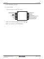
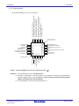
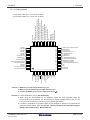
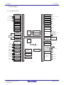
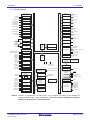
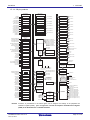
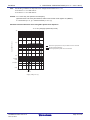
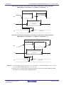
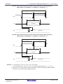
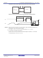
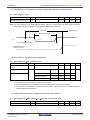
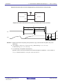
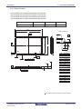
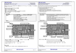
1.3 Pin Configuration (Top View)
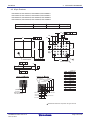
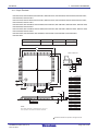
1.3.1 20-pin products
• 20-pin plastic LSSOP (7.62 mm (300), 0.65 mm pitch)
P01/ANI16/TO00/RxD1
P00/ANI17/TI00/TxD1
P40/TOOL0
RESET
P137/INTP0
P122/X2/EXCLK
P121/X1
REGC
VSS
VDD
1
2
3
4
5
6
7
8
9
10
20
19
18
17
16
15
14
13
12
11
P20/ANI0/AVREFP
P21/ANI1/AVREFM
P22/ANI2
P147/ANI18
P10/SCK00/SCL00
P11/SI00/RxD0/TOOLRxD/SDA00
P12/SO00/TxD0/TOOLTxD
P16/TI01/TO01/INTP5/SO11
P17/TI02/TO02/SI11/SDA11
P30/INTP3/SCK11/SCL11
Caution Connect the REGC pin to Vss via a capacitor (0.47 to 1 μF).
Remark For pin identification, see 1.4 Pin Identification.
R01DS0131EJ0310 Rev.3.10
Nov 15, 2013
Page 16 of 194
RL78/G13
1. OUTLINE
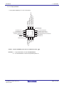
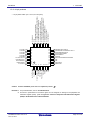
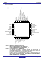
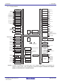
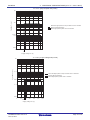
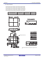
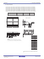
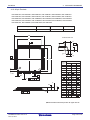
1.3.2 24-pin products
P22/ANI2
P147/ANI18
P10/SCK00/SCL00
P11/SI00/RxD0/TOOLRxD/SDA00
P12/SO00/TxD0/TOOLTxD
P16/TI01/TO01/INTP5
• 24-pin plastic HWQFN (4 × 4 mm, 0.5 mm pitch)
exposed die pad
P21/ANI1/AVREFM
P20/ANI0/AVREFP
P01/ANI16/TO00/RxD1
P00/ANI17/TI00/TxD1
P40/TOOL0
RESET
18 17 16 15 14 13
19
12
20
11
21
10
22
9
23
8
24
7
1 2 3 4 5 6
P17/TI02/TO02/SO11
P50/INTP1/SI11/SDA11
P30/INTP3/SCK11/SCL11
P31/TI03/TO03/INTP4/PCLBUZ0
P61/SDAA0
P60/SCLA0
P137/INTP0
P122/X2/EXCLK
P121/X1
REGC
VSS
VDD
INDEX MARK
Caution Connect the REGC pin to Vss via a capacitor (0.47 to 1 μF).
Remarks 1.
2.
For pin identification, see 1.4 Pin Identification.
It is recommended to connect an exposed die pad to Vss.
R01DS0131EJ0310 Rev.3.10
Nov 15, 2013
Page 17 of 194
RL78/G13
1. OUTLINE
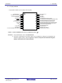
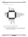
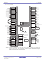
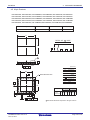
1.3.3 25-pin products
• 25-pin plastic WFLGA (3 × 3 mm, 0.50 mm pitch)
Bottom View
Top View
5
4
3
2
1
A
B
C
D
E
E
A
B
RESET
5
4
P122/X2/
EXCLK
P137/INTP0
P121/X1
VDD
3
REGC
VSS
2
P60/SCLA0
P61/SDAA0
1
A
B
C
B
A
INDEX MARK
INDEX MARK
P40/TOOL0
D
C
D
E
P01/ANI16/
TO00/RxD1
P22/ANI2
P147/ANI18
P00/ANI17/
TI00/TxD1
P21/ANI1/
AVREFM
P10/SCK00/
SCL00
P20/ANI0/
AVREFP
P12/SO00/
TxD0/
TOOLTxD
P30/INTP3/
SCK11/SCL11
P17/TI02/
TO02/SO11
P11/SI00/
RxD0/
TOOLRxD/
SDA00
P50/INTP1/
SI11/SDA11
P31/TI03/
TO03/INTP4/
PCLBUZ0
P16/TI01/
TO01/INTP5
5
C
D
4
3
2
P130
1
E
Caution Connect the REGC pin to Vss via a capacitor (0.47 to 1 μF).
Remark For pin identification, see 1.4 Pin Identification.
R01DS0131EJ0310 Rev.3.10
Nov 15, 2013
Page 18 of 194
RL78/G13
1. OUTLINE
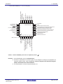
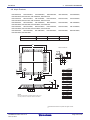
1.3.4 30-pin products
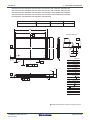
• 30-pin plastic LSSOP (7.62 mm (300), 0.65 mm pitch)
P20/ANI0/AVREFP
P01/ANI16/TO00/RxD1
P00/ANI17/TI00/TxD1
P120/ANI19
P40/TOOL0
RESET
P137/INTP0
P122/X2/EXCLK
P121/X1
REGC
VSS
VDD
P60/SCLA0
P61/SDAA0
P31/TI03/TO03/INTP4/PCLBUZ0
1
2
3
4
5
6
7
8
9
10
11
12
13
14
15
30
29
28
27
26
25
24
23
22
21
20
19
18
17
16
P21/ANI1/AVREFM
P22/ANI2
P23/ANI3
P147/ANI18
P10/SCK00/SCL00/(TI07)/(TO07)
P11/SI00/RxD0/TOOLRxD/SDA00/(TI06)/(TO06)
P12/SO00/TxD0/TOOLTxD/(TI05)/(TO05)
P13/TxD2/SO20/(SDAA0)/(TI04)/(TO04)
P14/RxD2/SI20/SDA20/(SCLA0)/(TI03)/(TO03)
P15/PCLBUZ1/SCK20/SCL20/(TI02)/(TO02)
P16/TI01/TO01/INTP5/(RXD0)
P17/TI02/TO02/(TXD0)
P51/INTP2/SO11
P50/INTP1/SI11/SDA11
P30/INTP3/SCK11/SCL11
Caution Connect the REGC pin to Vss via a capacitor (0.47 to 1 μF).
Remarks 1. For pin identification, see 1.4 Pin Identification.
2. Functions in parentheses in the above figure can be assigned via settings in the peripheral I/O
redirection register (PIOR). Refer to Figure 4-8 Format of Peripheral I/O Redirection Register
(PIOR) in the RL78/G13 User’s Manual Hardware.
R01DS0131EJ0310 Rev.3.10
Nov 15, 2013
Page 19 of 194
RL78/G13
1. OUTLINE
1.3.5 32-pin products
P10/SCK00/SCL00/(TI07)/(TO07)
P11/SI00/RxD0/TOOLRxD/SDA00/(TI06)/(TO06)
P12/SO00/TxD0/TOOLTxD/(TI05)/(TO05)
P13/TxD2/SO20/(SDAA0)/(TI04)/(TO04)
P14/RxD2/SI20/SDA20/(SCLA0)/(TI03)/(TO03)
P15/PCLBUZ1/SCK20/SCL20/(TI02)/(TO02)
P16/TI01/TO01/INTP5/(RXD0)
P17/TI02/TO02/(TXD0)
• 32-pin plastic HWQFN (5 × 5 mm, 0.5 mm pitch)
exposed die pad
P147/ANI18
P23/ANI3
P22/ANI2
P21/ANI1/AVREFM
P20/ANI0/AVREFP
P01/ANI16/TO00/RxD1
P00/ANI17/TI00/TxD1
P120/ANI19
24 23 22 21 20 19 18 17
25
16
26
15
27
14
28
13
29
12
30
11
31
10
32
9
1 2 3 4 5 6 7 8
P51/INTP2/SO11
P50/INTP1/SI11/SDA11
P30/INTP3/SCK11/SCL11
P70
P31/TI03/TO03/INTP4/PCLBUZ0
P62
P61/SDAA0
P60/SCLA0
P40/TOOL0
RESET
P137/INTP0
P122/X2/EXCLK
P121/X1
REGC
VSS
VDD
INDEX MARK
Caution Connect the REGC pin to Vss via a capacitor (0.47 to 1 μF).
Remarks 1. For pin identification, see 1.4 Pin Identification.
2. Functions in parentheses in the above figure can be assigned via settings in the peripheral I/O
redirection register (PIOR). Refer to Figure 4-8 Format of Peripheral I/O Redirection Register
(PIOR) in the RL78/G13 User’s Manual Hardware.
3. It is recommended to connect an exposed die pad to Vss.
R01DS0131EJ0310 Rev.3.10
Nov 15, 2013
Page 20 of 194
RL78/G13
1. OUTLINE
1.3.6 36-pin products
• 36-pin plastic WFLGA (4 × 4 mm, 0.5 mm pitch)
Top View
Bottom View
6
5
4
3
2
1
A
B
C
D
E
F
F
E
D
C
B
A
INDEX MARK
A
P60/SCLA0
B
VDD
C
P121/X1
D
P122/X2/EXCLK
E
P137/INTP0
F
P40/TOOL0
6
6
P62
P61/SDAA0
VSS
REGC
RESET
P120/ANI19
5
5
P71/SI21/
SDA21
P14/RxD2/SI20/
SDA20/(SCLA0)
/(TI03)/(TO03)
P31/TI03/TO03/
INTP4/
PCLBUZ0
P00/TI00/TxD1
P50/INTP1/
SI11/SDA11
P70/SCK21/
SCL21
P15/PCLBUZ1/
SCK20/SCL20/
(TI02)/(TO02)
P22/ANI2
P20/ANI0/
AVREFP
P21/ANI1/
AVREFM
P30/INTP3/
SCK11/SCL11
P16/TI01/TO01/
INTP5/(RxD0)
P12/SO00/
TxD0/TOOLTxD
/(TI05)/(TO05)
P24/ANI4
P23/ANI3
P51/INTP2/
SO11
P17/TI02/TO02/
(TxD0)
P13/TxD2/
SO20/(SDAA0)/
(TI04)/(TO04)
P11/SI00/RxD0/
TOOLRxD/
SDA00/(TI06)/
(TO06)
P10/SCK00/
SCL00/(TI07)/
(TO07)
B
C
D
P72/SO21
4
3
2
1
A
P01/TO00/RxD1
4
3
2
P147/ANI18
P25/ANI5
1
E
F
Caution Connect the REGC pin to Vss via a capacitor (0.47 to 1 μF).
Remarks 1. For pin identification, see 1.4 Pin Identification.
2. Functions in parentheses in the above figure can be assigned via settings in the peripheral I/O
redirection register (PIOR). Refer to Figure 4-8 Format of Peripheral I/O Redirection Register
(PIOR) in the RL78/G13 User’s Manual Hardware.
R01DS0131EJ0310 Rev.3.10
Nov 15, 2013
Page 21 of 194
RL78/G13
1. OUTLINE
1.3.7 40-pin products
P147/ANI18
P10/SCK00/SCL00/(TI07)/(TO07)
P11/SI00/RxD0/TOOLRxD/SDA00/(TI06)/(TO06)
P12/SO00/TxD0/TOOLTxD/(TI05)/(TO05)
P13/TxD2/SO20/(SDAA0)/(TI04)/(TO04)
P14/RxD2/SI20/SDA20/(SCLA0)/(TI03)/(TO03)
P15/PCLBUZ1/SCK20/SCL20/(TI02)/(TO02)
P16/TI01/TO01/INTP5/(RXD0)
P17/TI02/TO02/(TXD0)
P51/INTP2/SO11
• 40-pin plastic HWQFN (6 × 6 mm, 0.5 mm pitch)
P26/ANI6
P25/ANI5
P24/ANI4
P23/ANI3
P22/ANI2
P21/ANI1/AVREFM
P20/ANI0/AVREFP
P01/TO00/RxD1
P00/TI00/TxD1
P120/ANI19
30 29 28 27 26 25 24 23 22 21
31
20
exposed die pad
32
19
33
18
34
17
35
16
36
15
37
14
38
13
39
12
40
11
1 2 3 4 5 6 7 8 9 10
P50/INTP1/SI11/SDA11
P30/INTP3/RTC1HZ/SCK11/SCL11
P70/KR0/SCK21/SCL21
P71/KR1/SI21/SDA21
P72/KR2/SO21
P73/KR3
P31/TI03/TO03/INTP4/PCLBUZ0
P62
P61/SDAA0
P60/SCLA0
P40/TOOL0
RESET
P124/XT2/EXCLKS
P123/XT1
P137/INTP0
P122/X2/EXCLK
P121/X1
REGC
VSS
VDD
INDEX MARK
Caution Connect the REGC pin to Vss via a capacitor (0.47 to 1 μF).
Remarks 1. For pin identification, see 1.4 Pin Identification.
2. Functions in parentheses in the above figure can be assigned via settings in the peripheral I/O
redirection register (PIOR). Refer to Figure 4-8 Format of Peripheral I/O Redirection Register
(PIOR) in the RL78/G13 User’s Manual Hardware.
3. It is recommended to connect an exposed die pad to Vss.
R01DS0131EJ0310 Rev.3.10
Nov 15, 2013
Page 22 of 194
RL78/G13
1. OUTLINE
1.3.8 44-pin products
P147/ANI18
P146
P10/SCK00/SCL00/(TI07)/(TO07)
P11/SI00/RxD0/TOOLRxD/SDA00/(TI06)/(TO06)
P12/SO00/TxD0/TOOLTxD/(TI05)/(TO05)
P13/TxD2/SO20/(SDAA0)/(TI04)/(TO04)
P14/RxD2/SI20/SDA20/(SCLA0)/(TI03)/(TO03)
P15/PCLBUZ1/SCK20/SCL20/(TI02)/(TO02)
P16/TI01/TO01/INTP5/(RXD0)
P17/TI02/TO02/(TXD0)
P51/INTP2/SO11
• 44-pin plastic LQFP (10 × 10 mm, 0.8 mm pitch)
33 32 31 30 29 28 27 26 25 24 23
34
35
36
37
38
39
40
41
42
43
44
22
21
20
19
18
17
16
15
14
13
12
1 2 3 4 5 6 7 8 9 10 11
P50/INTP1/SI11/SDA11
P30/INTP3/RTC1HZ/SCK11/SCL11
P70/KR0/SCK21/SCL21
P71/KR1/SI21/SDA21
P72/KR2/SO21
P73/KR3
P31/TI03/TO03/INTP4/PCLBUZ0
P63
P62
P61/SDAA0
P60/SCLA0
P41/TI07/TO07
P40/TOOL0
RESET
P124/XT2/EXCLKS
P123/XT1
P137/INTP0
P122/X2/EXCLK
P121/X1
REGC
VSS
VDD
P27/ANI7
P26/ANI6
P25/ANI5
P24/ANI4
P23/ANI3
P22/ANI2
P21/ANI1/AVREFM
P20/ANI0/AVREFP
P01/TO00/RxD1
P00/TI00/TxD1
P120/ANI19
Caution Connect the REGC pin to Vss via a capacitor (0.47 to 1 μF).
Remarks 1. For pin identification, see 1.4 Pin Identification.
2. Functions in parentheses in the above figure can be assigned via settings in the peripheral I/O
redirection register (PIOR). Refer to Figure 4-8 Format of Peripheral I/O Redirection Register
(PIOR) in the RL78/G13 User’s Manual Hardware.
R01DS0131EJ0310 Rev.3.10
Nov 15, 2013
Page 23 of 194
RL78/G13
1. OUTLINE
1.3.9 48-pin products
P140/PCLBUZ0/INTP6
P00/TI00/TxD1
P01/TO00/RxD1
P130
P20/ANI0/AVREFP
P21/ANI1/AVREFM
P22/ANI2
P23/ANI3
P24/ANI4
P25/ANI5
P26/ANI6
P27/ANI7
• 48-pin plastic LFQFP (7 × 7 mm, 0.5 mm pitch)
36 35 34 33 32 31 30 29 28 27 26 25
24
37
23
38
22
39
21
40
20
41
19
42
18
43
17
44
16
45
15
46
14
47
13
48
1 2 3 4 5 6 7 8 9 10 11 12
P147/ANI18
P146
P10/SCK00/SCL00/(TI07)/(TO07)
P11/SI00/RxD0/TOOLRxD/SDA00/(TI06)/(TO06)
P12/SO00/TxD0/TOOLTxD/(TI05)/(TO05)
P13/TxD2/SO20/(SDAA0)/(TI04)/(TO04)
P14/RxD2/SI20/SDA20/(SCLA0)/(TI03)/(TO03)
P15/PCLBUZ1/SCK20/SCL20/(TI02)/(TO02)
P16/TI01/TO01/INTP5/(RXD0)
P17/TI02/TO02/(TXD0)
P51/INTP2/SO11
P50/INTP1/SI11/SDA11
P60/SCLA0
P61/SDAA0
P62
P63
P31/TI03/TO03/INTP4/(PCLBUZ0)
P75/KR5/INTP9/SCK01/SCL01
P74/KR4/INTP8/SI01/SDA01
P73/KR3/SO01
P72/KR2/SO21
P71/KR1/SI21/SDA21
P70/KR0/SCK21/SCL21
P30/INTP3/RTC1HZ/SCK11/SCL11
P120/ANI19
P41/TI07/TO07
P40/TOOL0
RESET
P124/XT2/EXCLKS
P123/XT1
P137/INTP0
P122/X2/EXCLK
P121/X1
REGC
VSS
VDD
Caution Connect the REGC pin to Vss via a capacitor (0.47 to 1 μF).
Remarks 1. For pin identification, see 1.4 Pin Identification.
2. Functions in parentheses in the above figure can be assigned via settings in the peripheral I/O
redirection register (PIOR). Refer to Figure 4-8 Format of Peripheral I/O Redirection Register
(PIOR) in the RL78/G13 User’s Manual Hardware.
R01DS0131EJ0310 Rev.3.10
Nov 15, 2013
Page 24 of 194
RL78/G13
1. OUTLINE
P140/PCLBUZ0/INTP6
P00/TI00/TxD1
P01/TO00/RxD1
P130
P20/ANI0/AVREFP
P21/ANI1/AVREFM
P22/ANI2
P23/ANI3
P24/ANI4
P25/ANI5
P26/ANI6
P27/ANI7
• 48-pin plastic HWQFN (7 × 7 mm, 0.5 mm pitch)
P120/ANI19
P41/TI07/TO07
P40/TOOL0
RESET
P124/XT2/EXCLKS
P123/XT1
P137/INTP0
P122/X2/EXCLK
P121/X1
REGC
VSS
VDD
36 35 34 33 32 31 30 29 28 27 26 25
37
24
38
23
exposed die pad
22
39
40
21
41
20
42
19
43
18
44
17
45
16
46
15
14
47
48
13
1 2 3 4 5 6 7 8 9 10 11 12
P147/ANI18
P146
P10/SCK00/SCL00/(TI07)/(TO07)
P11/SI00/RxD0/TOOLRxD/SDA00/(TI06)/(TO06)
P12/SO00/TxD0/TOOLTxD/(TI05)/(TO05)
P13/TxD2/SO20/(SDAA0)/(TI04)/(TO04)
P14/RxD2/SI20/SDA20/(SCLA0)/(TI03)/(TO03)
P15/PCLBUZ1/SCK20/SCL20/(TI02)/(TO02)
P16/TI01/TO01/INTP5/(RXD0)
P17/TI02/TO02/(TXD0)
P51/INTP2/SO11
P50/INTP1/SI11/SDA11
P60/SCLA0
P61/SDAA0
P62
P63
P31/TI03/TO03/INTP4/(PCLBUZ0)
P75/KR5/INTP9/SCK01/SCL01
P74/KR4/INTP8/SI01/SDA01
P73/KR3/SO01
P72/KR2/SO21
P71/KR1/SI21/SDA21
P70/KR0/SCK21/SCL21
P30/INTP3/RTC1HZ/SCK11/SCL11
INDEX MARK
Caution Connect the REGC pin to Vss via a capacitor (0.47 to 1 μF).
Remarks 1. For pin identification, see 1.4 Pin Identification.
2. Functions in parentheses in the above figure can be assigned via settings in the peripheral I/O
redirection register (PIOR). Refer to Figure 4-8 Format of Peripheral I/O Redirection Register
(PIOR) in the RL78/G13 User’s Manual Hardware.
3. It is recommended to connect an exposed die pad to Vss.
R01DS0131EJ0310 Rev.3.10
Nov 15, 2013
Page 25 of 194
RL78/G13
1. OUTLINE
1.3.10 52-pin products
P30/INTP3/RTC1HZ/SCK11/SCL11
P50/INTP1/SI11/SDA11
P51/INTP2/SO11
P17/TI02/TO02/(TXD0)
P16/TI01/TO01/INTP5/(RXD0)
P15/PCLBUZ1/SCK20/SCL20/(TI02)/(TO02)
P14/RxD2/SI20/SDA20/(SCLA0)/(TI03)/(TO03)
P13/TxD2/SO20/(SDAA0)/(TI04)/(TO04)
P12/SO00/TxD0/TOOLTxD/(TI05)/(TO05)
P11/SI00/RxD0/TOOLRxD/SDA00/(TI06)/(TO06)
P10/SCK00/SCL00/(TI07)/(TO07)
P146
P147/ANI18
• 52-pin plastic LQFP (10 × 10 mm, 0.65 mm pitch)
39 38 37 36 35 34 33 32 31 30 29 28 27
42
24
P72/KR2/SO21
P24/ANI4
43
23
P73/KR3/SO01
P23/ANI3
44
22
P74/KR4/INTP8/SI01/SDA01
P22/ANI2
45
21
P75/KR5/INTP9/SCK01/SCL01
P21/ANI1/AVREFM
46
20
P76/KR6/INTP10/(RXD2)
P20/ANI0/AVREFP
47
19
P77/KR7/INTP11/(TXD2)
P130
48
18
P31/TI03/TO03/INTP4/(PCLBUZ0)
P03/ANI16/RxD1
49
17
P63
P02/ANI17/TxD1
50
16
P62
P01/TO00
51
15
P61/SDAA0
P00/TI00
52
14
P60/SCLA0
VDD
VSS
8 9 10 11 12 13
REGC
6 7
P121/X1
5
P122/X2/EXCLK
3 4
P123/XT1
2
P40/TOOL0
P140/PCLBUZ0/INTP6
1
P137/INTP0
P71/KR1/SI21/SDA21
P25/ANI5
P124/XT2/EXCLKS
P70/KR0/SCK21/SCL21
25
RESET
26
41
P120/ANI19
40
P26/ANI6
P41/TI07/TO07
P27/ANI7
Caution Connect the REGC pin to Vss via a capacitor (0.47 to 1 μF).
Remarks 1. For pin identification, see 1.4 Pin Identification.
2. Functions in parentheses in the above figure can be assigned via settings in the peripheral I/O
redirection register (PIOR). Refer to Figure 4-8 Format of Peripheral I/O Redirection Register
(PIOR) in the RL78/G13 User’s Manual Hardware.
R01DS0131EJ0310 Rev.3.10
Nov 15, 2013
Page 26 of 194
RL78/G13
1. OUTLINE
1.3.11 64-pin products
• 64-pin plastic LQFP (12 × 12 mm, 0.65 mm pitch)
P147/ANI18
P146
P10/SCK00/SCL00/(TI07)/(TO07)
P11/SI00/RxD0/TOOLRxD/SDA00/(TI06)/(TO06)
P12/SO00/TxD0/TOOLTxD/(INTP5)/(TI05)/(TO05)
P13/TxD2/SO20/(SDAA0)/(TI04)/(TO04)
P14/RxD2/SI20/SDA20/(SCLA0)/(TI03)/(TO03)
P15/SCK20/SCL20/(TI02)/(TO02)
P16/TI01/TO01/INTP5/(SI00)/(RXD0)
P17/TI02/TO02/(SO00)/(TXD0)
P55/(PCLBUZ1)/(SCK00)
P54
P53/(INTP11)
P52/(INTP10)
P51/INTP2/SO11
P50/INTP1/SI11/SDA11
• 64-pin plastic LFQFP (10 × 10 mm, 0.5 mm pitch)
48 47 46 45 44 43 42 41 40 39 38 37 36 35 34 33
P27/ANI7
P26/ANI6
P25/ANI5
P24/ANI4
P23/ANI3
P22/ANI2
P21/ANI1/AVREFM
P20/ANI0/AVREFP
P130
P04/SCK10/SCL10
P03/ANI16/SI10/RxD1/SDA10
P02/ANI17/SO10/TxD1
P01/TO00
P00/TI00
P141/PCLBUZ1/INTP7
P140/PCLBUZ0/INTP6
49
50
51
52
53
54
55
56
57
58
59
60
61
62
63
64
32
31
30
29
28
27
26
25
24
23
22
21
20
19
18
17
6 7 8 9 10 11 12 13 14 15 16
P120/ANI19
P43
P42/TI04/TO04
P41/TI07/TO07
P40/TOOL0
RESET
P124/XT2/EXCLKS
P123/XT1
P137/INTP0
P122/X2/EXCLK
P121/X1
REGC
VSS
EVSS0
VDD
EVDD0
1 2 3 4 5
P30/INTP3/RTC1HZ/SCK11/SCL11
P05/TI05/TO05
P06/TI06/TO06
P70/KR0/SCK21/SCL21
P71/KR1/SI21/SDA21
P72/KR2/SO21
P73/KR3/SO01
P74/KR4/INTP8/SI01/SDA01
P75/KR5/INTP9/SCK01/SCL01
P76/KR6/INTP10/(RXD2)
P77/KR7/INTP11/(TXD2)
P31/TI03/TO03/INTP4/(PCLBUZ0)
P63
P62
P61/SDAA0
P60/SCLA0
Cautions 1. Make EVSS0 pin the same potential as VSS pin.
2. Make VDD pin the potential that is higher than EVDD0 pin.
3. Connect the REGC pin to Vss via a capacitor (0.47 to 1 μF).
Remarks 1. For pin identification, see 1.4 Pin Identification.
2. When using the microcontroller for an application where the noise generated inside the
microcontroller must be reduced, it is recommended to supply separate powers to the VDD and
EVDD0 pins and connect the VSS and EVSS0 pins to separate ground lines.
3. Functions in parentheses in the above figure can be assigned via settings in the peripheral I/O
redirection register (PIOR). Refer to Figure 4-8 Format of Peripheral I/O Redirection Register
(PIOR) in the RL78/G13 User’s Manual Hardware.
R01DS0131EJ0310 Rev.3.10
Nov 15, 2013
Page 27 of 194
RL78/G13
1. OUTLINE
• 64-pin plastic VFBGA (4 × 4 mm, 0.4 mm pitch)
Top View
Bottom View
8
7
6
5
4
3
2
1
A
B
C D E
F
G H
H
G
F
E D
C
B A
Index mark
Pin No.
Name
Pin No.
Name
Pin No.
Name
Pin No.
Name
A1
P05/TI05/TO05
C1
P51/INTP2/SO11
E1
P13/TxD2/SO20/
G1
(SDAA0)/(TI04)/(TO04)
P146
A2
P30/INTP3/RTC1HZ
/SCK11/SCL11
C2
P71/KR1/SI21/SDA21
E2
P14/RxD2/SI20/SDA20 G2
/(SCLA0)/(TI03)/(TO03)
P25/ANI5
A3
P70/KR0/SCK21
/SCL21
C3
P74/KR4/INTP8/SI01
/SDA01
E3
P15/SCK20/SCL20/
(TI02)/(TO02)
G3
P24/ANI4
A4
P75/KR5/INTP9
/SCK01/SCL01
C4
P52/(INTP10)
E4
P16/TI01/TO01/INTP5 G4
/(SI00)/(RxD0)
P22/ANI2
A5
P77/KR7/INTP11/
(TxD2)
C5
P53/(INTP11)
E5
P03/ANI16/SI10/RxD1 G5
/SDA10
P130
A6
P61/SDAA0
C6
P63
E6
P41/TI07/TO07
P02/ANI17/SO10/TxD1
A7
P60/SCLA0
C7
VSS
E7
RESET
G7
P00/TI00
A8
EVDD0
C8
P121/X1
E8
P137/INTP0
G8
P124/XT2/EXCLKS
B1
P50/INTP1/SI11
/SDA11
D1
P55/(PCLBUZ1)/
(SCK00)
F1
P10/SCK00/SCL00/
(TI07)/(TO07)
H1
P147/ANI18
B2
P72/KR2/SO21
D2
P06/TI06/TO06
F2
P11/SI00/RxD0
/TOOLRxD/SDA00/
(TI06)/(TO06)
H2
P27/ANI7
B3
P73/KR3/SO01
D3
P17/TI02/TO02/
(SO00)/(TxD0)
F3
P12/SO00/TxD0
/TOOLTxD/(INTP5)/
H3
P26/ANI6
G6
(TI05)/(TO05)
B4
P76/KR6/INTP10/
(RxD2)
D4
P54
F4
P21/ANI1/AVREFM
H4
P23/ANI3
B5
P31/TI03/TO03
/INTP4/(PCLBUZ0)
D5
P42/TI04/TO04
F5
P04/SCK10/SCL10
H5
P20/ANI0/AVREFP
B6
P62
D6
P40/TOOL0
F6
P43
H6
P141/PCLBUZ1/INTP7
B7
VDD
D7
REGC
F7
P01/TO00
H7
P140/PCLBUZ0/INTP6
B8
EVSS0
D8
P122/X2/EXCLK
F8
P123/XT1
H8
P120/ANI19
Cautions 1. Make EVSS0 pin the same potential as VSS pin.
2. Make VDD pin the potential that is higher than EVDD0 pin.
3. Connect the REGC pin to Vss via a capacitor (0.47 to 1 μF).
Remarks 1. For pin identification, see 1.4 Pin Identification.
2. When using the microcontroller for an application where the noise generated inside the
microcontroller must be reduced, it is recommended to supply separate powers to the VDD and
EVDD0 pins and connect the VSS and EVSS0 pins to separate ground lines.
3. Functions in parentheses in the above figure can be assigned via settings in the peripheral I/O
redirection register (PIOR). Refer to Figure 4-8 Format of Peripheral I/O Redirection Register
(PIOR) in the RL78/G13 User’s Manual Hardware.
R01DS0131EJ0310 Rev.3.10
Nov 15, 2013
Page 28 of 194
RL78/G13
1. OUTLINE
1.3.12 80-pin products
• 80-pin plastic LQFP (14 × 14 mm, 0.65 mm pitch)
P153/ANI11
P100/ANI20
P147/ANI18
P146
P111/(INTP11)
P110/(INTP10)
P10/SCK00/SCL00/(TI07)/(TO07)
P11/SI00/RxD0/TOOLRxD/SDA00/(TI06)/(TO06)
P12/SO00/TxD0/TOOLTxD/(INTP5)/(TI05)/(TO05)
P13/TxD2/SO20/(SDAA0)/(TI04)/(TO04)
P14/RxD2/SI20/SDA20/(SCLA0)/(TI03)/(TO03)
P15/SCK20/SCL20/(TI02)/(TO02)
P16/TI01/TO01/INTP5/(SI00)/(RXD0)
P17/TI02/TO02/(SO00)/(TXD0)
P55/(PCLBUZ1)/(SCK00)
P54/SCK31/SCL31
P53/SI31/SDA31
P52/SO31
P51/INTP2/SO11
P50/INTP1/SI11/SDA11
• 80-pin plastic LFQFP (12 × 12 mm, 0.5 mm pitch)
60 59 58 57 56 55 54 53 52 51 50 49 48 47 46 45 44 43 42 41
P152/ANI10
P151/ANI9
P150/ANI8
P27/ANI7
P26/ANI6
P25/ANI5
P24/ANI4
P23/ANI3
P22/ANI2
P21/ANI1/AVREFM
P20/ANI0/AVREFP
P130
P04/SCK10/SCL10
P03/ANI16/SI10/RxD1/SDA10
P02/ANI17/SO10/TxD1
P01/TO00
P00/TI00
P144/SO30/TxD3
P143/SI30/RxD3/SDA30
P142/SCK30/SCL30
40
39
38
37
36
35
34
33
32
31
30
29
28
27
26
25
24
23
22
21
61
62
63
64
65
66
67
68
69
70
71
72
73
74
75
76
77
78
79
80
P30/INTP3/RTC1HZ/SCK11/SCL11
P05/TI05/TO05
P06/TI06/TO06
P70/KR0/SCK21/SCL21
P71/KR1/SI21/SDA21
P72/KR2/SO21
P73/KR3
P74/KR4/INTP8
P75/KR5/INTP9
P76/KR6/INTP10/(RXD2)
P77/KR7/INTP11/(TXD2)
P67/TI13/TO13
P66/TI12/TO12
P65/TI11/TO11
P64/TI10/TO10
P31/TI03/TO03/INTP4/(PCLBUZ0)
P63/SDAA1
P62/SCLA1
P61/SDAA0
P60/SCLA0
P141/PCLBUZ1/INTP7
P140/PCLBUZ0/INTP6
P120/ANI19
P45/SO01
P44/SI01/SDA01
P43/SCK01/SCL01
P42/TI04/TO04
P41/TI07/TO07
P40/TOOL0
RESET
P124/XT2/EXCLKS
P123/XT1
P137/INTP0
P122/X2/EXCLK
P121/X1
REGC
VSS
EVSS0
VDD
EVDD0
1 2 3 4 5 6 7 8 9 10 11 12 13 14 15 16 17 18 19 20
Cautions 1. Make EVSS0 pin the same potential as VSS pin.
2. Make VDD pin the potential that is higher than EVDD0 pin.
3. Connect the REGC pin to Vss via a capacitor (0.47 to 1 μF).
Remarks 1. For pin identification, see 1.4 Pin Identification.
2. When using the microcontroller for an application where the noise generated inside the
microcontroller must be reduced, it is recommended to supply separate powers to the VDD and
EVDD0 pins and connect the VSS and EVSS0 pins to separate ground lines.
3. Functions in parentheses in the above figure can be assigned via settings in the peripheral I/O
redirection register (PIOR). Refer to Figure 4-8 Format of Peripheral I/O Redirection Register
(PIOR) in the RL78/G13 User’s Manual Hardware.
R01DS0131EJ0310 Rev.3.10
Nov 15, 2013
Page 29 of 194
RL78/G13
1. OUTLINE
1.3.13 100-pin products
P100/ANI20
P147/ANI18
P146/(INTP4)
P111/(INTP11)
P110/(INTP10)
P101
P10/SCK00/SCL00/(TI07)/(TO07)
P11/SI00/RxD0/TOOLRxD/SDA00/(TI06)/(TO06)
P12/SO00/TxD0/TOOLTxD/(INTP5)/(TI05)/(TO05)
P13/TxD2/SO20/(SDAA0)/(TI04)/(TO04)
P14/RxD2/SI20/SDA20/(SCLA0)/(TI03)/(TO03)
P15/SCK20/SCL20/(TI02)/(TO02)
P16/TI01/TO01/INTP5/(SI00)/(RXD0)
P17/TI02/TO02/(SO00)/(TXD0)
P57/(INTP3)
P56/(INTP1)
P55/(PCLBUZ1)/(SCK00)
P54/SCK31/SCL31
P53/SI31/SDA31
P52/SO31
P51/SO11
P50/SI11/SDA11
EVDD1
P30/INTP3/RTC1HZ/SCK11/SCL11
P87/(INTP9)
• 100-pin plastic LQFP (14 × 14 mm, 0.65 mm pitch)
75 74 73 72 71 70 69 68 67 66 65 64 63 62 61 60 59 58 57 56 55 54 53 52 51
50
76
49
77
48
78
47
79
46
80
45
81
44
82
43
83
42
84
41
85
40
86
39
87
38
88
37
89
36
90
35
91
34
92
33
93
32
94
31
95
30
96
29
97
28
98
27
99
26
100
1 2 3 4 5 6 7 8 9 10 11 12 13 14 15 16 17 18 19 20 21 22 23 24 25
P86/(INTP8)
P85/(INTP7)
P84/(INTP6)
P83
P82/(SO10)/(TXD1)
P81/(SI10)/(RXD1)/(SDA10)
P80/(SCK10)/(SCL10)
EVSS1
P05
P06
P70/KR0/SCK21/SCL21
P71/KR1/SI21/SDA21
P72/KR2/SO21
P73/KR3
P74/KR4/INTP8
P75/KR5/INTP9
P76/KR6/INTP10/(RXD2)
P77/KR7/INTP11/(TXD2)
P67/TI13/TO13
P66/TI12/TO12
P65/TI11/TO11
P64/TI10/TO10
P31/TI03/TO03/INTP4/(PCLBUZ0)
P63/SDAA1
P62/SCLA1
P142/SCK30/SCL30
P141/PCLBUZ1/INTP7
P140/PCLBUZ0/INTP6
P120/ANI19
P47/INTP2
P46/INTP1/TI05/TO05
P45/SO01
P44/SI01/SDA01
P43/SCK01/SCL01
P42/TI04/TO04
P41
P40/TOOL0
RESET
P124/XT2/EXCLKS
P123/XT1
P137/INTP0
P122/X2/EXCLK
P121/X1
REGC
VSS
EVSS0
VDD
EVDD0
P60/SCLA0
P61/SDAA0
P156/ANI14
P155/ANI13
P154/ANI12
P153/ANI11
P152/ANI10
P151/ANI9
P150/ANI8
P27/ANI7
P26/ANI6
P25/ANI5
P24/ANI4
P23/ANI3
P22/ANI2
P21/ANI1/AVREFM
P20/ANI0/AVREFP
P130
P102/TI06/TO06
P04/SCK10/SCL10
P03/ANI16/SI10/RxD1/SDA10
P02/ANI17/SO10/TxD1
P01/TO00
P00/TI00
P145/TI07/TO07
P144/SO30/TxD3
P143/SI30/RxD3/SDA30
Cautions 1. Make EVSS0, EVSS1 pins the same potential as VSS pin.
2. Make VDD pin the potential that is higher than EVDD0, EVDD1 pins (EVDD0 = EVDD1).
3. Connect the REGC pin to Vss via a capacitor (0.47 to 1 μF).
Remarks 1. For pin identification, see 1.4 Pin Identification.
2. When using the microcontroller for an application where the noise generated inside the
microcontroller must be reduced, it is recommended to supply separate powers to the VDD, EVDD0
and EVDD1 pins and connect the VSS, EVSS0 and EVSS1 pins to separate ground lines.
3. Functions in parentheses in the above figure can be assigned via settings in the peripheral I/O
redirection register (PIOR). Refer to Figure 4-8 Format of Peripheral I/O Redirection Register
(PIOR) in the RL78/G13 User’s Manual Hardware.
R01DS0131EJ0310 Rev.3.10
Nov 15, 2013
Page 30 of 194
RL78/G13
1. OUTLINE
P140/PCLBUZ0/INTP6
P141/PCLBUZ1/INTP7
P142/SCK30/SCL30
P143/SI30/RxD3/SDA30
P144/SO30/TxD3
P145/TI07/TO07
P00/TI00
P01/TO00
P02/ANI17/SO10/TxD1
P03/ANI16/SI10/RxD1/SDA10
P04/SCK10/SCL10
P102/TI06/TO06
P130
P20/ANI0/AVREFP
P21/ANI1/AVREFM
P22/ANI2
P23/ANI3
P24/ANI4
P25/ANI5
P26/ANI6
P27/ANI7
P150/ANI8
P151/ANI9
P152/ANI10
P153/ANI11
P154/ANI12
P155/ANI13
P156/ANI14
P100/ANI20
P147/ANI18
• 100-pin plastic LQFP (14 × 20 mm, 0.65 mm pitch)
80 79 78 77 76 75 74 73 72 71 70 69 68 67 66 65 64 63 62 61 60 59 58 57 56 55 54 53 52 51
50
81
49
82
48
83
47
84
46
85
45
86
44
87
43
88
42
89
41
90
40
91
39
92
38
93
37
94
36
95
35
96
34
97
33
98
32
99
31
100
1 2 3 4 5 6 7 8 9 10 11 12 13 14 15 16 17 18 19 20 21 22 23 24 25 26 27 28 29 30
P146/(INTP4)
P111/(INTP11)
P110/(INTP10)
P101
P10/SCK00/SCL00/(TI07)/(TO07)
P11/SI00/RxD0/TOOLRxD/SDA00/(TI06)/(TO06)
P12/SO00/TxD0/TOOLTxD/(INTP5)/(TI05)/(TO05)
P13/TxD2/SO20/(SDAA0)/(TI04)/(TO04)
P14/RxD2/SI20/SDA20/(SCLA0)/(TI03)/(TO03)
P15/SCK20/SCL20/(TI02)/(TO02)
P16/TI01/TO01/INTP5/(SI00)/(RXD0)
P17/TI02/TO02/(SO00)/(TXD0)
P57/(INTP3)
P56/(INTP1)
P55/(PCLBUZ1)/(SCK00)
P54/SCK31/SCL31
P53/SI31/SDA31
P52/SO31
P51/SO11
P50/SI11/SDA11
P60/SCLA0
P61/SDAA0
P62/SCLA1
P63/SDAA1
P31/TI03/TO03/INTP4/(PCLBUZ0)
P64/TI10/TO10
P65/TI11/TO11
P66/TI12/TO12
P67/TI13/TO13
P77/KR7/INTP11/(TXD2)
P76/KR6/INTP10/(RXD2)
P75/KR5/INTP9
P74/KR4/INTP8
P73/KR3
P72/KR2/SO21
P71/KR1/SI21/SDA21
P70/KR0/SCK21/SCL21
P06
P05
EVSS1
P80/(SCK10)/(SCL10)
P81/(SI10)/(RXD1)/(SDA10)
P82/(SO10)/(TXD1)
P83
P84/(INTP6)
P85/(INTP7)
P86/(INTP8)
P87/(INTP9)
P30/INTP3/RTC1HZ/SCK11/SCL11
EVDD1
P120/ANI19
P47/INTP2
P46/INTP1/TI05/TO05
P45/SO01
P44/SI01/SDA01
P43/SCK01/SCL01
P42/TI04/TO04
P41
P40/TOOL0
RESET
P124/XT2/EXCLKS
P123/XT1
P137/INTP0
P122/X2/EXCLK
P121/X1
REGC
VSS
EVSS0
VDD
EVDD0
Cautions 1. Make EVSS0, EVSS1 pins the same potential as VSS pin.
2. Make VDD pin the potential that is higher than EVDD0, EVDD1 pins (EVDD0 = EVDD1).
3. Connect the REGC pin to Vss via a capacitor (0.47 to 1 μF).
Remarks 1. For pin identification, see 1.4 Pin Identification.
2. When using the microcontroller for an application where the noise generated inside the
microcontroller must be reduced, it is recommended to supply separate powers to the VDD, EVDD0
and EVDD1 pins and connect the VSS, EVSS0 and EVSS1 pins to separate ground lines.
3. Functions in parentheses in the above figure can be assigned via settings in the peripheral I/O
redirection register (PIOR). Refer to Figure 4-8 Format of Peripheral I/O Redirection Register
(PIOR) in the RL78/G13 User’s Manual Hardware.
R01DS0131EJ0310 Rev.3.10
Nov 15, 2013
Page 31 of 194
RL78/G13
1. OUTLINE
1.3.14 128-pin products
P100/ANI20
P147/ANI18
P146/(INTP4)
P111/(INTP11)
P110/(INTP10)
P101
P117/ANI24
P116/ANI25
P115/ANI26
P114
P113
P112
P97/SO11
P96/SI11/SDA11
P95/SCK11/SCL11
P94
P93
P92
P91
P90
P10/SCK00/SCL00/(TI07)/(TO07)
P11/SI00/RxD0/TOOLRxD/SDA00/(TI06)/(TO06)
P12/SO00/TxD0/TOOLTxD/(INTP5)/(TI05)/(TO05)
P13/TxD2/SO20/(SDAA0)/(TI04)/(TO04)
P14/RxD2/SI20/SDA20/(SCLA0)/(TI03)/(TO03)
P15/SCK20/SCL20/(TI02)/(TO02)
P16/TI01/TO01/INTP5/(SI00)/(RXD0)
P17/TI02/TO02/(SO00)/(TXD0)
P57/(INTP3)
P56/(INTP1)
P55/(PCLBUZ1)/(SCK00)
P54/SCK31/SCL31
P53/SI31/SDA31
P52/SO31
P51
P50
P30/INTP3/RTC1HZ
P87/(INTP9)
• 128-pin plastic LFQFP (14 × 20 mm, 0.5 mm pitch)
102 101 100 99 98 97 96 95 94 93 92 91 90 89 88 87 86 85 84 83 82 81 80 79 78 77 76 75 74 73 72 71 70 69 68 67 66 65
103
64
104
63
105
62
106
61
107
60
108
59
109
58
110
57
111
56
112
55
113
54
114
53
115
52
51
116
50
117
49
118
48
119
47
120
46
121
45
122
44
123
43
124
42
125
41
126
40
127
39
128
1 2 3 4 5 6 7 8 9 10 11 12 13 14 15 16 17 18 19 20 21 22 23 24 25 26 27 28 29 30 31 32 33 34 35 36 37 38
P86/(INTP8)
P85/(INTP7)
P84/(INTP6)
P83
P82/(SO10)/(TXD1)
P81/(SI10)/(RXD1)/(SDA10)
P80/(SCK10)/(SCL10)
EVDD1
EVSS1
P05
P06
P70/KR0/SCK21/SCL21
P71/KR1/SI21/SDA21
P72/KR2/SO21
P73/KR3
P74/KR4/INTP8
P75/KR5/INTP9
P76/KR6/INTP10/(RXD2)
P77/KR7/INTP11/(TXD2)
P67/TI13/TO13
P66/TI12/TO12
P65/TI11/TO11
P64/TI10/TO10
P31/TI03/TO03/INTP4/(PCLBUZ0)
P63/SDAA1
P62/SCLA1
P142/SCK30/SCL30
P141/PCLBUZ1/INTP7
P140/PCLBUZ0/INTP6
P120/ANI19
P37/ANI21
P36/ANI22
P35/ANI23
P34
P33
P32
P106/TI17/TO17
P105/TI16/TO16
P104/TI15/TO15
P103/TI14/TO14
P47/INTP2
P46/INTP1/TI05/TO05
P45/SO01
P44/SI01/SDA01
P43/SCK01/SCL01
P42/TI04/TO04
P41
P40/TOOL0
P127
P126
P125
RESET
P124/XT2/EXCLKS
P123/XT1
P137/INTP0
P122/X2/EXCLK
P121/X1
REGC
VSS
EVSS0
VDD
EVDD0
P60/SCLA0
P61/SDAA0
P156/ANI14
P155/ANI13
P154/ANI12
P153/ANI11
P152/ANI10
P151/ANI9
P150/ANI8
P27/ANI7
P26/ANI6
P25/ANI5
P24/ANI4
P23/ANI3
P22/ANI2
P21/ANI1/AVREFM
P20/ANI0/AVREFP
P130
P102/TI06/TO06
P07
P04/SCK10/SCL10
P03/ANI16/SI10/RxD1/SDA10
P02/ANI17/SO10/TxD1
P01/TO00
P00/TI00
P145/TI07/TO07
P144/SO30/TxD3
P143/SI30/RxD3/SDA30
Cautions 1. Make EVSS0, EVSS1 pins the same potential as VSS pin.
2. Make VDD pin the potential that is higher than EVDD0, EVDD1 pins (EVDD0 = EVDD1).
3. Connect the REGC pin to Vss via a capacitor (0.47 to 1 μF).
Remarks 1. For pin identification, see 1.4 Pin Identification.
2. When using the microcontroller for an application where the noise generated inside the
microcontroller must be reduced, it is recommended to supply separate powers to the VDD, EVDD0
and EVDD1 pins and connect the VSS, EVSS0 and EVSS1 pins to separate ground lines.
3. Functions in parentheses in the above figure can be assigned via settings in the peripheral I/O
redirection register (PIOR). Refer to Figure 4-8 Format of Peripheral I/O Redirection Register
(PIOR) in the RL78/G13 User’s Manual Hardware.
R01DS0131EJ0310 Rev.3.10
Nov 15, 2013
Page 32 of 194
RL78/G13
1. OUTLINE
1.4 Pin Identification
ANI0 to ANI14,
REGC:
Regulator capacitance
ANI16 to ANI26:
Analog input
RESET:
Reset
AVREFM:
A/D converter reference
RTC1HZ:
Real-time clock correction clock
(1 Hz) output
potential (− side) input
A/D converter reference
RxD0 to RxD3:
potential (+ side) input
SCK00, SCK01, SCK10,
EVDD0, EVDD1:
Power supply for port
SCK11, SCK20, SCK21,
EVSS0, EVSS1:
Ground for port
SCLA0, SCLA1:
EXCLK:
External clock input (Main SCLA0, SCLA1, SCL00,
AVREFP:
Receive data
Serial clock input/output
system clock)
SCL01, SCL10, SCL11,
External clock input
SCL20,SCL21, SCL30,
(Subsystem clock)
SCL31:
Interrupt request from
SDAA0, SDAA1, SDA00,
peripheral
SDA01,SDA10, SDA11,
KR0 to KR7:
Key return
SDA20,SDA21, SDA30,
P00 to P07:
Port 0
SDA31:
P10 to P17:
Port 1
SI00, SI01, SI10, SI11,
P20 to P27:
Port 2
SI20, SI21, SI30, SI31:
P30 to P37:
Port 3
SO00, SO01, SO10,
P40 to P47:
Port 4
SO11, SO20, SO21,
P50 to P57:
Port 5
SO30, SO31:
P60 to P67:
Port 6
TI00 to TI07,
P70 to P77:
Port 7
TI10 to TI17:
P80 to P87:
Port 8
TO00 to TO07,
P90 to P97:
Port 9
TO10 to TO17:
Timer output
P100 to P106:
Port 10
TOOL0:
Data input/output for tool
P110 to P117:
Port 11
TOOLRxD, TOOLTxD:
Data input/output for external device
P120 to P127:
Port 12
TxD0 to TxD3:
Transmit data
P130, P137:
Port 13
VDD:
Power supply
P140 to P147:
Port 14
VSS:
Ground
P150 to P156:
Port 15
X1, X2:
Crystal oscillator (main system clock)
XT1, XT2:
Crystal oscillator (subsystem clock)
EXCLKS:
INTP0 to INTP11:
PCLBUZ0, PCLBUZ1: Programmable clock
Serial clock output
Serial data input/output
Serial data input
Serial data output
Timer input
output/buzzer output
R01DS0131EJ0310 Rev.3.10
Nov 15, 2013
Page 33 of 194
RL78/G13
1. OUTLINE
1.5 Block Diagram
1.5.1 20-pin products
TIMER ARRAY
UNIT (8ch)
PORT 0
2
P00, P01
TI00/P00
TO00/P01
ch0
PORT 1
5
P10 to P12, P16, P17
TI01/TO01/P16
ch1
PORT 2
3
P20 to P22
TI02/TO02/P17
ch2
PORT 3
P30
PORT 4
P40
ch3
ch4
PORT 12
ch5
ch6
ch7
WINDOW
WATCHDOG
TIMER
LOW-SPEED
ON-CHIP
OSCILLATOR
RL78
CPU
CORE
P121, P122
PORT 13
P137
PORT 14
P147
CODE FLASH MEMORY
DATA FLASH MEMORY
2
A/D CONVERTER
3
ANI0/P20 to
ANI2/P22
3
ANI16/P01, ANI17/P00,
ANI18/P147
AVREFP/P20
AVREFM/P21
12-BIT INTERVAL
TIMER
POWER ON RESET/
VOLTAGE
DETECTOR
REAL-TIME
CLOCK
POR/LVD
CONTROL
RAM
SERIAL ARRAY
UNIT0 (4ch)
RxD0/P11
TxD0/P12
RESET CONTROL
ON-CHIP DEBUG
UART0
VDD
RxD1/P01
TxD1/P00
VSS TOOLRxD/P11,
TOOLTxD/P12
UART1
SYSTEM
CONTROL
HIGH-SPEED
ON-CHIP
SCK00/P10
SI00/P11
SO00/P12
CSI00
SCK11/P30
SI11/P17
SO11/P16
CSI11
SCL00/P10
SDA00/P11
IIC00
SCL11/P30
SDA11/P17
IIC11
R01DS0131EJ0310 Rev.3.10
Nov 15, 2013
MULTIPLIER&
DIVIDER,
MULITIPLYACCUMULATOR
CRC
OSCILLATOR
VOLTAGE
REGULATOR
DIRECT MEMORY
ACCESS CONTROL
BCD
ADJUSTMENT
TOOL0/P40
RESET
X1/P121
X2/EXCLK/P122
REGC
INTP0/P137
INTERRUPT
CONTROL
INTP3/P30
INTP5/P16
Page 34 of 194
RL78/G13
1. OUTLINE
1.5.2 24-pin products
TIMER ARRAY
UNIT (8ch)
PORT 0
2
P00, P01
TI00/P00
TO00/P01
ch0
PORT 1
5
P10 to P12, P16, P17
TI01/TO01/P16
ch1
PORT 2
3
P20 to P22
TI02/TO02/P17
ch2
PORT 3
2
P30, P31
TI03/TO03/P31
ch3
PORT 4
P40
PORT 5
P50
ch4
ch5
ch6
ch7
WINDOW
WATCHDOG
TIMER
LOW-SPEED
ON-CHIP
OSCILLATOR
12-BIT INTERVAL
TIMER
RL78
CPU
CORE
PORT 6
2
P60, P61
PORT 12
2
P121, P122
PORT 13
P137
PORT 14
P147
CODE FLASH MEMORY
3
ANI0/P20 to
ANI2/P22
3
ANI16/P01, ANI17/P00,
ANI18/P147
DATA FLASH MEMORY
A/D CONVERTER
REAL-TIME
CLOCK
SERIAL ARRAY
UNIT0 (4ch)
RxD0/P11
TxD0/P12
UART0
RxD1/P01
TxD1/P00
UART1
SCK00/P10
SI00/P11
SO00/P12
CSI00
SCK11/P30
SI11/P50
SO11/P17
CSI11
AVREFP/P20
AVREFM/P21
POWER ON RESET/
VOLTAGE
DETECTOR
RAM
POR/LVD
CONTROL
RESET CONTROL
VDD
VSS TOOLRxD/P11,
TOOLTxD/P12
TOOL0/P40
ON-CHIP DEBUG
SYSTEM
CONTROL
SERIAL
INTERFACE IICA0
SDAA0/P61
SCLA0/P60
RESET
X1/P121
HIGH-SPEED
ON-CHIP
X2/EXCLK/P122
OSCILLATOR
SCL00/P10
SDA00/P11
IIC00
SCL11/P30
SDA11/P50
IIC11
BUZZER OUTPUT
PCLBUZ0/P31
CLOCK OUTPUT
CONTROL
DIRECT MEMORY
ACCESS CONTROL
BCD
ADJUSTMENT
MULTIPLIER&
DIVIDER,
MULITIPLYACCUMULATOR
VOLTAGE
REGULATOR
REGC
INTP0/P137
CRC
INTP1/P50
INTERRUPT
CONTROL
2
INTP3/P30,
INTP4/P31
INTP5/P16
R01DS0131EJ0310 Rev.3.10
Nov 15, 2013
Page 35 of 194
RL78/G13
1. OUTLINE
1.5.3 25-pin products
TIMER ARRAY
UNIT (8ch)
PORT 0
2
P00, P01
TI00/P00
TO00/P01
ch0
PORT 1
5
P10 to P12, P16, P17
TI01/TO01/P16
ch1
PORT 2
3
P20 to P22
TI02/TO02/P17
ch2
PORT 3
2
P30, P31
TI03/TO03/P31
ch3
PORT 4
P40
PORT 5
P50
ch4
ch5
ch6
ch7
WINDOW
WATCHDOG
TIMER
LOW-SPEED
ON-CHIP
OSCILLATOR
12-BIT INTERVAL
TIMER
RL78
CPU
CORE
PORT 6
2
P60, P61
PORT 12
2
P121, P122
PORT 13
P130
P137
PORT 14
P147
CODE FLASH MEMORY
3
ANI0/P20 to
ANI2/P22
3
ANI16/P01, ANI17/P00,
ANI18/P147
DATA FLASH MEMORY
A/D CONVERTER
AVREFP/P20
AVREFM/P21
REAL-TIME
CLOCK
SERIAL ARRAY
UNIT0 (4ch)
RxD0/P11
TxD0/P12
UART0
RxD1/P01
TxD1/P00
UART1
SCK00/P10
SI00/P11
SO00/P12
CSI00
SCK11/P30
SI11/P50
SO11/P17
CSI11
POWER ON RESET/
VOLTAGE
DETECTOR
RAM
POR/LVD
CONTROL
RESET CONTROL
VDD
VSS TOOLRxD/P11,
TOOLTxD/P12
TOOL0/P40
ON-CHIP DEBUG
SYSTEM
CONTROL
SCL00/P10
SDA00/P11
IIC00
SCL11/P30
SDA11/P50
IIC11
SERIAL
INTERFACE IICA0
SDAA0/P61
SCLA0/P60
RESET
X1/P121
HIGH-SPEED
ON-CHIP
X2/EXCLK/P122
OSCILLATOR
BUZZER OUTPUT
PCLBUZ0/P31
CLOCK OUTPUT
CONTROL
DIRECT MEMORY
ACCESS CONTROL
BCD
ADJUSTMENT
MULTIPLIER&
DIVIDER,
MULITIPLYACCUMULATOR
VOLTAGE
REGULATOR
REGC
INTP0/P137
CRC
INTP1/P50
INTERRUPT
CONTROL
2
INTP3/P30,
INTP4/P31
INTP5/P16
R01DS0131EJ0310 Rev.3.10
Nov 15, 2013
Page 36 of 194
RL78/G13
1. OUTLINE
1.5.4 30-pin products
TIMER ARRAY
UNIT (8ch)
PORT 0
2
P00, P01
TI00/P00
TO00/P01
ch0
PORT 1
8
P10 to P17
TI01/TO01/P16
ch1
PORT 2
4
P20 to P23
TI02/TO02/P17
(TI02/TO02/P15)
ch2
PORT 3
2
P30, P31
TI03/TO03/P31
(TI03/TO03/P14)
ch3
(TI04/TO04/P13)
ch4
(TI05/TO05/P12)
ch5
(TI06/TO06/P11)
ch6
(TI07/TO07/P10)
RxD2/P14
ch7
PORT 4
LOW-SPEED
ON-CHIP
OSCILLATOR
PORT 5
2
P50, P51
PORT 6
2
P60, P61
PORT 12
WINDOW
WATCHDOG
TIMER
RxD0/P11(RxD0/P16)
TxD0/P12(TxD0/P17)
UART0
RxD1/P01
TxD1/P00
UART1
SCK00/P10
SI00/P11
SO00/P12
CSI00
SCK11/P30
SI11/P50
SO11/P51
CSI11
SCL00/P10
SDA00/P11
IIC00
P137
PORT 14
P147
4
ANI0/P20 to
ANI3/P23
4
ANI16/P01, ANI17/P00,
ANI18/P147, ANI19/P120
CODE FLASH MEMORY
RL78
CPU
CORE
A/D CONVERTER
AVREFP/P20
AVREFM/P21
DATA FLASH MEMORY
POWER ON RESET/
VOLTAGE
DETECTOR
POR/LVD
CONTROL
RAM
RESET CONTROL
VDD
VSS TOOLRxD/P11,
TOOLTxD/P12
SDAA0/P61(SDAA0/P13)
SERIAL
INTERFACE IICA0
SCLA0/P60(SCLA0/P14)
IIC11
BUZZER OUTPUT
2
SERIAL ARRAY
UNIT1 (2ch)
UART2
LINSEL
SCK20/P15
SI20/P14
SO20/P13
CSI20
SCL20/P15
SDA20/P14
IIC20
Remark
P121, P122
12-BIT INTERVAL
TIMER
SERIAL ARRAY
UNIT0 (4ch)
RxD2/P14
TxD2/P13
P120
2
PORT 13
REAL-TIME
CLOCK
SCL11/P30
SDA11/P50
P40
CLOCK OUTPUT
CONTROL
PCLBUZ0/P31,
PCLBUZ1/P15
MULTIPLIER&
DIVIDER,
MULITIPLYACCUMULATOR
DIRECT MEMORY
ACCESS CONTROL
BCD
ADJUSTMENT
TOOL0/P40
ON-CHIP DEBUG
SYSTEM
CONTROL
RESET
X1/P121
HIGH-SPEED
ON-CHIP
OSCILLATOR
X2/EXCLK/P122
VOLTAGE
REGULATOR
REGC
CRC
RxD2/P14
INTP0/P137
INTERRUPT
CONTROL
2
2
INTP1/P50,
INTP2/P51
INTP3/P30,
INTP4/P31
INTP5/P16
Functions in parentheses in the above figure can be assigned via settings in the peripheral I/O
redirection register (PIOR). Refer to Figure 4-8 Format of Peripheral I/O Redirection Register
(PIOR) in the RL78/G13 User’s Manual Hardware.
R01DS0131EJ0310 Rev.3.10
Nov 15, 2013
Page 37 of 194
RL78/G13
1. OUTLINE
1.5.5 32-pin products
TIMER ARRAY
UNIT (8ch)
PORT 0
2
P00, P01
TI00/P00
TO00/P01
ch0
PORT 1
8
P10 to P17
TI01/TO01/P16
ch1
PORT 2
4
P20 to P23
TI02/TO02/P17
(TI02/TO02/P15)
ch2
PORT 3
2
P30, P31
TI03/TO03/P31
(TI03/TO03/P14)
ch3
(TI04/TO04/P13)
ch4
(TI05/TO05/P12)
ch5
(TI06/TO06/P11)
(TI07/TO07/P10)
RxD2/P14
PORT 4
PORT 5
2
P50, P51
ch6
PORT 6
3
P60 to P62
ch7
PORT 7
PORT 12
WINDOW
WATCHDOG
TIMER
LOW-SPEED
ON-CHIP
OSCILLATOR
12-BIT INTERVAL
TIMER
REAL-TIME
CLOCK
RxD0/P11(RxD0/P16)
TxD0/P12(TxD0/P17)
UART0
RxD1/P01
TxD1/P00
UART1
SCK00/P10
SI00/P11
SO00/P12
CSI00
P120
P121, P122
2
PORT 13
P137
PORT 14
P147
DATA FLASH MEMORY
A/D CONVERTER
4
ANI0/P20 to
ANI3/P23
4
ANI16/P01, ANI17/P00,
ANI18/P147, ANI19/P120
AVREFP/P20
AVREFM/P21
POWER ON RESET/
VOLTAGE
DETECTOR
RAM
POR/LVD
CONTROL
RESET CONTROL
VDD
SCK11/P30
SI11/P50
SO11/P51
CSI11
SCL00/P10
SDA00/P11
IIC00
SCL11/P30
SDA11/P50
IIC11
VSS TOOLRxD/P11,
TOOLTxD/P12
TOOL0/P40
ON-CHIP DEBUG
SDAA0/P61(SDAA0/P13)
SERIAL
INTERFACE IICA0
SCLA0/P60(SCLA0/P14)
BUZZER OUTPUT
2
CLOCK OUTPUT
CONTROL
SERIAL ARRAY
UNIT1 (2ch)
LINSEL
MULTIPLIER&
DIVIDER,
MULITIPLYACCUMULATOR
SCK20/P15
SI20/P14
SO20/P13
CSI20
DIRECT MEMORY
ACCESS CONTROL
SCL20/P15
SDA20/P14
IIC20
BCD
ADJUSTMENT
Remark
P70
CODE FLASH MEMORY
RL78
CPU
CORE
SERIAL ARRAY
UNIT0 (4ch)
RxD2/P14
TxD2/P13
P40
UART2
PCLBUZ0/P31,
PCLBUZ1/P15
CRC
SYSTEM
CONTROL
RESET
X1/P121
HIGH-SPEED
ON-CHIP
OSCILLATOR
X2/EXCLK/P122
VOLTAGE
REGULATOR
REGC
RxD2/P14
INTP0/P137
INTERRUPT
CONTROL
2
2
INTP1/P50,
INTP2/P51
INTP3/P30,
INTP4/P31
INTP5/P16
Functions in parentheses in the above figure can be assigned via settings in the peripheral I/O
redirection register (PIOR). Refer to Figure 4-8 Format of Peripheral I/O Redirection Register
(PIOR) in the RL78/G13 User’s Manual Hardware.
R01DS0131EJ0310 Rev.3.10
Nov 15, 2013
Page 38 of 194
RL78/G13
1. OUTLINE
1.5.6 36-pin products
TIMER ARRAY
UNIT (8ch)
PORT 0
2
P00, P01
TI00/P00
TO00/P01
ch0
PORT 1
8
P10 to P17
TI01/TO01/P16
ch1
PORT 2
6
P20 to P25
TI02/TO02/P17
(TI02/TO02/P15)
ch2
PORT 3
2
P30, P31
TI03/TO03/P31
(TI03/TO03/P14)
ch3
(TI04/TO04/P13)
ch4
(TI05/TO05/P12)
ch5
(TI06/TO06/P11)
(TI07/TO07/P10)
RxD2/P14
PORT 4
PORT 5
2
P50, P51
ch6
PORT 6
3
P60 to P62
ch7
PORT 7
3
P70 to P72
2
P121, P122
WINDOW
WATCHDOG
TIMER
LOW-SPEED
ON-CHIP
OSCILLATOR
PORT 12
RxD0/P11(RxD0/P16)
TxD0/P12(TxD0/P17)
UART0
RxD1/P01
TxD1/P00
UART1
SCK00/P10
SI00/P11
SO00/P12
CSI00
SCK11/P30
SI11/P50
SO11/P51
CSI11
SCL00/P10
SDA00/P11
IIC00
SCL11/P30
SDA11/P50
IIC11
P137
PORT 14
P147
DATA FLASH MEMORY
A/D CONVERTER
POWER ON RESET/
VOLTAGE
DETECTOR
RAM
VSS TOOLRxD/P11,
TOOLTxD/P12
SDAA0/P61(SDAA0/P13)
CSI20
MULTIPLIER&
DIVIDER,
MULITIPLYACCUMULATOR
SCL21/P70
SDA21/P71
IIC21
SCLA0/P60(SCLA0/P14)
2
CLOCK OUTPUT
CONTROL
IIC20
ANI18/P147, ANI19/P120
POR/LVD
CONTROL
TOOL0/P40
ON-CHIP DEBUG
SYSTEM
CONTROL
RESET
X1/P121
X2/EXCLK/P122
HIGH-SPEED
ON-CHIP
OSCILLATOR
UART2
SCL20/P15
SDA20/P14
2
BUZZER OUTPUT
LINSEL
CSI21
ANI0/P20 to
ANI5/P25
RESET CONTROL
VDD
SERIAL ARRAY
UNIT1 (2ch)
6
AVREFP/P20
AVREFM/P21
SERIAL
INTERFACE IICA0
Remark
PORT 13
CODE FLASH MEMORY
RL78
CPU
CORE
SERIAL ARRAY
UNIT0 (4ch)
SCK20/P15
SI20/P14
SO20/P13
SCK21/P70
SI21/P71
SO21/P72
P120
12-BIT INTERVAL
TIMER
REAL-TIME
CLOCK
RxD2/P14
TxD2/P13
P40
PCLBUZ0/P31,
PCLBUZ1/P15
VOLTAGE
REGULATOR
REGC
RxD2/P14
INTP0/P137
CRC
INTERRUPT
CONTROL
2
2
DIRECT MEMORY
ACCESS CONTROL
INTP1/P50,
INTP2/P51
INTP3/P30,
INTP4/P31
INTP5/P16
BCD
ADJUSTMENT
Functions in parentheses in the above figure can be assigned via settings in the peripheral I/O
redirection register (PIOR). Refer to Figure 4-8 Format of Peripheral I/O Redirection Register
(PIOR) in the RL78/G13 User’s Manual Hardware.
R01DS0131EJ0310 Rev.3.10
Nov 15, 2013
Page 39 of 194
RL78/G13
1. OUTLINE
1.5.7 40-pin products
TIMER ARRAY
UNIT (8ch)
PORT 0
2
P00, P01
TI00/P00
TO00/P01
ch0
PORT 1
8
P10 to P17
TI01/TO01/P16
ch1
PORT 2
7
P20 to P26
TI02/TO02/P17
(TI02/TO02/P15)
ch2
PORT 3
2
P30, P31
TI03/TO03/P31
(TI03/TO03/P14)
ch3
(TI04/TO04/P13)
ch4
(TI05/TO05/P12)
ch5
(TI06/TO06/P11)
(TI07/TO07/P10)
RxD2/P14
PORT 4
PORT 5
2
P50, P51
ch6
PORT 6
3
P60 to P62
ch7
PORT 7
4
P70 to P73
4
P121 to P124
WINDOW
WATCHDOG
TIMER
LOW-SPEED
ON-CHIP
OSCILLATOR
RTC1HZ/P30
PORT 12
REAL-TIME
CLOCK
RxD0/P11(RxD0/P16)
TxD0/P12(TxD0/P17)
UART0
RxD1/P01
TxD1/P00
UART1
CSI00
SCK11/P30
SI11/P50
SO11/P51
CSI11
SCL00/P10
SDA00/P11
IIC00
SCL11/P30
SDA11/P50
IIC11
P137
PORT 14
P147
CODE FLASH MEMORY
RL78
CPU
CORE
DATA FLASH MEMORY
A/D CONVERTER
POWER ON RESET/
VOLTAGE
DETECTOR
VSS TOOLRxD/P11,
TOOLTxD/P12
SDAA0/P61(SDAA0/P13)
CSI20
MULTIPLIER&
DIVIDER,
MULITIPLYACCUMULATOR
SCL21/P70
SDA21/P71
IIC21
KR0/P70 to
KR3/P73
4
POR/LVD
CONTROL
RESET CONTROL
TOOL0/P40
ON-CHIP DEBUG
SCLA0/P60(SCLA0/P14)
2
CLOCK OUTPUT
CONTROL
IIC20
ANI18/P147, ANI19/P120
SYSTEM
CONTROL
UART2
SCL20/P15
SDA20/P14
2
RESET
X1/P121
X2/EXCLK/P122
BUZZER OUTPUT
LINSEL
CSI21
ANI0/P20 to
ANI6/P26
RAM
VDD
SERIAL ARRAY
UNIT1 (2ch)
7
AVREFP/P20
AVREFM/P21
SERIAL
INTERFACE IICA0
Remark
PORT 13
KEY RETURN
SCK00/P10
SI00/P11
SO00/P12
SCK20/P15
SI20/P14
SO20/P13
SCK21/P70
SI21/P71
SO21/P72
P120
12-BIT INTERVAL
TIMER
SERIAL ARRAY
UNIT0 (4ch)
RxD2/P14
TxD2/P13
P40
PCLBUZ0/P31,
PCLBUZ1/P15
DIRECT MEMORY
ACCESS CONTROL
CRC
HIGH-SPEED
XT1/P123
ON-CHIP
OSCILLATOR
XT2/EXCLKS/P124
VOLTAGE
REGULATOR
REGC
RxD2/P14
INTP0/P137
INTERRUPT
CONTROL
2
2
BCD
ADJUSTMENT
INTP1/P50,
INTP2/P51
INTP3/P30,
INTP4/P31
INTP5/P16
Functions in parentheses in the above figure can be assigned via settings in the peripheral I/O
redirection register (PIOR). Refer to Figure 4-8 Format of Peripheral I/O Redirection Register
(PIOR) in the RL78/G13 User’s Manual Hardware.
R01DS0131EJ0310 Rev.3.10
Nov 15, 2013
Page 40 of 194
RL78/G13
1. OUTLINE
1.5.8 44-pin products
TIMER ARRAY
UNIT (8ch)
PORT 0
2
P00, P01
TI00/P00
TO00/P01
ch0
PORT 1
8
P10 to P17
TI01/TO01/P16
ch1
PORT 2
8
P20 to P27
TI02/TO02/P17
(TI02/TO02/P15)
ch2
PORT 3
2
P30, P31
TI03/TO03/P31
(TI03/TO03/P14)
ch3
PORT 4
2
P40, P41
(TI04/TO04/P13)
ch4
(TI05/TO05/P12)
ch5
PORT 5
2
P50, P51
(TI06/TO06/P11)
TI07/TO07/P41
(TI07/TO07/P10)
RxD2/P14
ch6
PORT 6
4
P60 to P63
ch7
PORT 7
4
P70 to P73
4
P121 to P124
WINDOW
WATCHDOG
TIMER
LOW-SPEED
ON-CHIP
OSCILLATOR
RTC1HZ/P30
PORT 12
PORT 13
TxD0/P12(TxD0/P17)
RxD1/P01
TxD1/P00
REAL-TIME
CLOCK
CODE FLASH MEMORY
RL78
CPU
CORE
DATA FLASH MEMORY
A/D CONVERTER
P146, P147
8
ANI0/P20 to
ANI7/P27
2
ANI18/P147, ANI19/P120
AVREFP/P20
AVREFM/P21
KEY RETURN
SCK11/P30
SI11/P50
SO11/P51
CSI11
SCL00/P10
SDA00/P11
IIC00
SCL11/P30
SDA11/P50
IIC11
KR0/P70 to
KR3/P73
4
RAM
POWER ON RESET/
VOLTAGE
DETECTOR
VDD
SERIAL ARRAY
UNIT1 (2ch)
POR/LVD
CONTROL
VSS TOOLRxD/P11,
TOOLTxD/P12
RESET CONTROL
SDAA0/P61(SDAA0/P13)
SERIAL
INTERFACE IICA0
UART2
SYSTEM
CONTROL
2
CLOCK OUTPUT
CONTROL
CSI20
MULTIPLIER&
DIVIDER,
MULITIPLYACCUMULATOR
TOOL0/P40
ON-CHIP DEBUG
SCLA0/P60(SCLA0/P14)
BUZZER OUTPUT
LINSEL
PCLBUZ0/P31,
PCLBUZ1/P15
RESET
X1/P121
X2/EXCLK/P122
HIGH-SPEED
XT1/P123
ON-CHIP
OSCILLATOR
CRC
XT2/EXCLKS/P124
VOLTAGE
REGULATOR
REGC
RxD2/P14
INTP0/P137
CSI21
SCL20/P15
SDA20/P14
IIC20
SCL21/P70
SDA21/P71
IIC21
Remark
2
UART1
CSI00
SCK20/P15
SI20/P14
SO20/P13
SCK21/P70
SI21/P71
SO21/P72
PORT 14
UART0
SCK00/P10
SI00/P11
SO00/P12
RxD2/P14
TxD2/P13
P137
12-BIT INTERVAL
TIMER
SERIAL ARRAY
UNIT0 (4ch)
RxD0/P11(RxD0/P16)
P120
DIRECT MEMORY
ACCESS CONTROL
INTERRUPT
CONTROL
2
2
BCD
ADJUSTMENT
INTP1/P50,
INTP2/P51
INTP3/P30,
INTP4/P31
INTP5/P16
Functions in parentheses in the above figure can be assigned via settings in the peripheral I/O
redirection register (PIOR). Refer to Figure 4-8 Format of Peripheral I/O Redirection Register
(PIOR) in the RL78/G13 User’s Manual Hardware.
R01DS0131EJ0310 Rev.3.10
Nov 15, 2013
Page 41 of 194
RL78/G13
1. OUTLINE
1.5.9 48-pin products
TIMER ARRAY
UNIT (8ch)
PORT 0
2
P00, P01
TI00/P00
TO00/P01
ch0
PORT 1
8
P10 to P17
TI01/TO01/P16
ch1
PORT 2
8
P20 to P27
TI02/TO02/P17
(TI02/TO02/P15)
ch2
PORT 3
2
P30, P31
TI03/TO03/P31
(TI03/TO03/P14)
ch3
PORT 4
2
P40, P41
(TI04/TO04/P13)
ch4
(TI05/TO05/P12)
ch5
PORT 5
2
P50, P51
(TI06/TO06/P11)
ch6
PORT 6
4
P60 to P63
TI07/TO07/P41
(TI07/TO07/P10)
RxD2/P14
ch7
PORT 7
6
P70 to P75
4
P121 to P124
PORT 12
WINDOW
WATCHDOG
TIMER
LOW-SPEED
ON-CHIP
OSCILLATOR
RTC1HZ/P30
PORT 14
REAL-TIME
CLOCK
RxD0/P11(RxD0/P16)
TxD0/P12(TxD0/P17)
UART0
RxD1/P01
TxD1/P00
UART1
DATA FLASH MEMORY
8
ANI0/P20 to
ANI7/P27
A/D CONVERTER
2
ANI18/P147, ANI19/P120
AVREFP/P20
AVREFM/P21
RAM
POWER ON RESET/
VOLTAGE
DETECTOR
CSI01
SCL00/P10
SDA00/P11
IIC00
SCL01/P75
SDA01/P74
IIC01
SCL11/P30
SDA11/P50
IIC11
VDD
KR0/P70 to
KR5/P75
6
VSS TOOLRxD/P11,
TOOLTxD/P12
POR/LVD
CONTROL
RESET CONTROL
TOOL0/P40
ON-CHIP DEBUG
SYSTEM
CONTROL
SERIAL ARRAY
UNIT1 (2ch)
SERIAL
INTERFACE IICA0
HIGH-SPEED
SCLA0/P60(SCLA0/P14)
BUZZER OUTPUT
CSI20
CLOCK OUTPUT
CONTROL
PCLBUZ0/P140
(PCLBUZ0/P31),
PCLBUZ1/P15
MULTIPLIER&
DIVIDER,
MULITIPLYACCUMULATOR
CSI21
DIRECT MEMORY
ACCESS CONTROL
SCL20/P15
SDA20/P14
IIC20
SCL21/P70
SDA21/P71
IIC21
RESET
X1/P121
X2/EXCLK/P122
SDAA0/P61(SDAA0/P13)
2
UART2
LINSEL
Remark
P140,
P146, P147
CSI00
CSI11
SCK20/P15
SI20/P14
SO20/P13
SCK21/P70
SI21/P71
SO21/P72
3
CODE FLASH MEMORY
RL78
CPU
CORE
KEY RETURN
SCK11/P30
SI11/P50
SO11/P51
RxD2/P14
TxD2/P13
P130
P137
PORT 13
12-BIT INTERVAL
TIMER
SERIAL ARRAY
UNIT0 (4ch)
SCK00/P10
SI00/P11
SO00/P12
SCK01/P75
SI01/P74
SO01/P73
P120
BCD
ADJUSTMENT
ON-CHIP
XT1/P123
OSCILLATOR
XT2/EXCLKS/P124
VOLTAGE
REGULATOR
REGC
RxD2/P14
INTP0/P137
CRC
2
INTERRUPT
CONTROL
2
INTP1/P50,
INTP2/P51
INTP3/P30,
INTP4/P31
INTP5/P16
INTP6/P140
2
INTP8/P74,
INTP9/P75
Functions in parentheses in the above figure can be assigned via settings in the peripheral I/O
redirection register (PIOR). Refer to Figure 4-8 Format of Peripheral I/O Redirection Register
(PIOR) in the RL78/G13 User’s Manual Hardware.
R01DS0131EJ0310 Rev.3.10
Nov 15, 2013
Page 42 of 194
RL78/G13
1. OUTLINE
1.5.10 52-pin products
TIMER ARRAY
UNIT (8ch)
PORT 0
4
P00 to P03
TI00/P00
TO00/P01
ch0
PORT 1
8
P10 to P17
TI01/TO01/P16
ch1
PORT 2
8
P20 to P27
TI02/TO02/P17
(TI02/TO02/P15)
ch2
PORT 3
2
P30, P31
TI03/TO03/P31
(TI03/TO03/P14)
ch3
PORT 4
2
P40, P41
(TI04/TO04/P13)
ch4
(TI05/TO05/P12)
ch5
PORT 5
2
P50, P51
(TI06/TO06/P11)
ch6
PORT 6
4
P60 to P63
TI07/TO07/P41
(TI07/TO07/P10)
RxD2/P14
(RxD2/P76)
ch7
PORT 7
8
P70 to P77
PORT 12
WINDOW
WATCHDOG
TIMER
P120
4
P121 to P124
P130
P137
PORT 13
LOW-SPEED
ON-CHIP
OSCILLATOR
RTC1HZ/P30
12-BIT INTERVAL
TIMER
REAL-TIME
CLOCK
SERIAL ARRAY
UNIT0 (4ch)
RxD0/P11(RxD0/P16)
TxD0/P12(TxD0/P17)
UART0
RxD1/P03
TxD1/P02
UART1
SCK00/P10
SI00/P11
SO00/P12
SCK01/P75
SI01/P74
SO01/P73
PORT 14
RL78
CPU
CORE
KEY RETURN
8
ANI16/P03, ANI17/P02,
ANI18/P147, ANI19/P120
AVREFP/P20
AVREFM/P21
DATA FLASH MEMORY
KR0/P70 to
KR7/P77
CSI00
POWER ON RESET/
VOLTAGE
DETECTOR
RAM
CSI01
IIC00
SCL01/P75
SDA01/P74
IIC01
SYSTEM
CONTROL
SCL11/P30
SDA11/P50
IIC11
HIGH-SPEED
POR/LVD
CONTROL
RESET CONTROL
VDD
VSS TOOLRxD/P11,
TOOLTxD/P12
TOOL0/P40
ON-CHIP DEBUG
RESET
X1/P121
X2/EXCLK/P122
XT1/P123
ON-CHIP
SDAA0/P61(SDAA0/P13)
SERIAL
INTERFACE IICA0
SERIAL ARRAY
UNIT1 (2ch)
LINSEL
OSCILLATOR
XT2/EXCLKS/P124
SCLA0/P60(SCLA0/P14)
VOLTAGE
REGULATOR
BUZZER OUTPUT
UART2
2
CLOCK OUTPUT
CONTROL
REGC
PCLBUZ0/P140
(PCLBUZ0/P31),
PCLBUZ1/P15
RxD2/P14 (RxD2/P76)
INTP0/P137
2
CSI20
CSI21
MULTIPLIER&
DIVIDER,
MULITIPLYACCUMULATOR
CRC
INTERRUPT
CONTROL
2
INTP1/P50,
INTP2/P51
INTP3/P30,
INTP4/P31
INTP5/P16
INTP6/P140
SCL20/P15
SDA20/P14
IIC20
SCL21/P70
SDA21/P71
IIC21
Remark
ANI0/P20 to
ANI7/P27
4
SCL00/P10
SDA00/P11
SCK20/P15
SI20/P14
SO20/P13
SCK21/P70
SI21/P71
SO21/P72
8
A/D CONVERTER
CSI11
TxD2/P13(TxD2/P77)
P140,
P146, P147
CODE FLASH MEMORY
SCK11/P30
SI11/P50
SO11/P51
RxD2/P14(RxD2/P76)
3
DIRECT MEMORY
ACCESS CONTROL
4
INTP8/P74 to
INTP11/P77
BCD
ADJUSTMENT
Functions in parentheses in the above figure can be assigned via settings in the peripheral I/O
redirection register (PIOR). Refer to Figure 4-8 Format of Peripheral I/O Redirection Register
(PIOR) in the RL78/G13 User’s Manual Hardware.
R01DS0131EJ0310 Rev.3.10
Nov 15, 2013
Page 43 of 194
RL78/G13
1. OUTLINE
1.5.11 64-pin products
TIMER ARRAY
UNIT (8ch)
PORT 0
7
P00 to P06
TI00/P00
TO00/P01
ch0
PORT 1
8
P10 to P17
PORT 2
8
P20 to P27
PORT 3
2
P30, P31
PORT 4
4
P40 to P43
PORT 5
6
P50 to P55
ch6
PORT 6
4
P60 to P63
ch7
PORT 7
8
P70 to P77
4
P121 to P124
TI01/TO01/P16
ch1
TI02/TO02/P17
(TI02/TO02/P15)
ch2
TI03/TO03/P31
(TI03/TO03/P14)
ch3
TI04/TO04/P42
(TI04/TO04/P13)
ch4
TI05/TO05/P05
(TI05/TO05/P12)
ch5
TI06/TO06/P06
(TI06/TO06/P11)
TI07/TO07/P41
(TI07/TO07/P10)
RxD2/P14
(RxD2/P76)
PORT 12
WINDOW
WATCHDOG
TIMER
LOW-SPEED
ON-CHIP
OSCILLATOR
P130
P137
PORT 13
12-BIT INTERVAL
TIMER
PORT 14
4
P140, P141,
P146, P147
8
ANI0/P20 to
ANI7/P27
REAL-TIME
CLOCK
RTC1HZ/P30
SERIAL ARRAY
UNIT0 (4ch)
RxD0/P11(RxD0/P16)
TxD0/P12(TxD0/P17)
UART0
RxD1/P03
TxD1/P02
UART1
SCK00/P10(SCK00/P55)
SI00/P11(SI00/P16)
SO00/P12(SO00/P17)
SCK01/P75
SI01/P74
SO01/P73
A/D CONVERTER
4
KEY RETURN
8
ANI16/P03, ANI17/P02,
ANI18/P147, ANI19/P120
AVREFP/P20
AVREFM/P21
CODE FLASH MEMORY
RL78
CPU
CORE
DATA FLASH MEMORY
KR0/P70 to
KR7/P77
CSI00
POWER ON RESET/
VOLTAGE
DETECTOR
CSI01
SCK10/P04
SI10/P03
SO10/P02
CSI10
SCK11/P30
SI11/P50
SO11/P51
CSI11
SCL00/P10
SDA00/P11
IIC00
SCL01/P75
SDA01/P74
IIC01
POR/LVD
CONTROL
RAM
RESET CONTROL
TOOL0/P40
ON-CHIP DEBUG
VDD, VSS, TOOLRxD/P11,
EVDD0 EVSS0 TOOLTxD/P12
SYSTEM
CONTROL
RESET
X1/P121
X2/EXCLK/P122
HIGH-SPEED
XT1/P123
ON-CHIP
SCL10/P04
SDA10/P03
IIC10
SCL11/P30
SDA11/P50
IIC11
SERIAL
INTERFACE IICA0
SDAA0/P61(SDAA0/P13)
BUZZER OUTPUT
PCLBUZ0/P140
(PCLBUZ0/P31),
PCLBUZ1/P141
(PCLBUZ1/P55)
RxD2/P14(RxD2/P76)
TxD2/P13(TxD2/P77)
SCK20/P15
SI20/P14
SO20/P13
SCK21/P70
SI21/P71
SO21/P72
OSCILLATOR
XT2/EXCLKS/P124
SCLA0/P60(SCLA0/P14)
VOLTAGE
REGULATOR
2
SERIAL ARRAY
UNIT1 (2ch)
Remark
P120
CLOCK OUTPUT
CONTROL
REGC
RxD2/P14 (RxD2/P76)
INTP0/P137
2
UART2
LINSEL
MULTIPLIER&
DIVIDER,
MULITIPLYACCUMULATOR
CSI20
DIRECT MEMORY
ACCESS CONTROL
CRC
2
INTERRUPT
CONTROL
INTP5/P16(INTP5/P12)
2
INTP6/P140,
INTP7/P141
2
INTP8/P74,
INTP9/P75
2
INTP10/P76(INTP10/P52),
INTP11/P77(INTP11/P53)
CSI21
SCL20/P15
SDA20/P14
IIC20
SCL21/P70
SDA21/P71
IIC21
BCD
ADJUSTMENT
INTP1/P50,
INTP2/P51
INTP3/P30,
INTP4/P31
Functions in parentheses in the above figure can be assigned via settings in the peripheral I/O
redirection register (PIOR). Refer to Figure 4-8 Format of Peripheral I/O Redirection Register
(PIOR) in the RL78/G13 User’s Manual Hardware.
R01DS0131EJ0310 Rev.3.10
Nov 15, 2013
Page 44 of 194
RL78/G13
1. OUTLINE
1.5.12 80-pin products
TIMER ARRAY
UNIT0 (8ch)
TIMER ARRAY
UNIT1 (4ch)
TI00/P00
TO00/P01
ch0
ch0
TI10/TO10/P64
PORT 0
7
P00 to P06
TI01/TO01/P16
ch1
ch1
TI11/TO11/P65
PORT 1
8
P10 to P17
TI02/TO02/P17
(TI02/TO02/P15)
ch2
ch2
TI12/TO12/P66
PORT 2
8
P20 to P27
TI03/TO03/P31
(TI03/TO03/P14)
ch3
ch3
TI13/TO13/P67
PORT 3
2
P30, P31
TI04/TO04/P42
(TI04/TO04/P13)
ch4
PORT 4
6
P40 to P45
TI05/TO05/P05
(TI05/TO05/P12)
ch5
PORT 5
6
P50 to P55
PORT 6
8
P60 to P67
PORT 7
8
P70 to P77
TI06/TO06/P06
(TI06/TO06/P11)
TI07/TO07/P41
(TI07/TO07/P10)
RxD2/P14
(RxD2/P76)
ch6
ch7
SERIAL ARRAY
UNIT0 (4ch)
RxD0/P11(RxD0/P16)
TxD0/P12(TxD0/P17)
UART0
RxD1/P03
TxD1/P02
UART1
SCK00/P10(SCK00/P55)
SI00/P11(SI00/P16)
SO00/P12(SO00/P17)
SCK01/P43
SI01/P44
SO01/P45
PORT 11
PORT 12
SCL00/P10
SDA00/P11
IIC00
SCL01/P43
SDA01/P44
IIC01
SCL10/P04
SDA10/P03
IIC10
SCL11/P30
SDA11/P50
IIC11
CODE FLASH MEMORY
RL78
CPU
CORE
SERIAL ARRAY
UNIT1 (4ch)
P110, P111
2
BUZZER OUTPUT
CSI21
CLOCK OUTPUT
CONTROL
PCLBUZ0/P140
(PCLBUZ0/P31),
PCLBUZ1/P141
(PCLBUZ1/P55)
2
IIC20
P140 to P144,
P146, P147
PORT 15
4
P150 to P153
KEY RETURN
8
KR0/P70 to
KR7/P77
POR/LVD
CONTROL
RESET CONTROL
CSI20
SCL20/P15
SDA20/P14
7
SDAA0/P61(SDAA0/P13)
SDAA1/P63
SCLA1/P62
CSI31
PORT 14
VDD, VSS, TOOLRxD/P11,
EVDD0 EVSS0 TOOLTxD/P12
UART3
SCK31/P54
SI31/P53
SO31/P52
P130
P137
PORT 13
POWER ON RESET/
VOLTAGE
DETECTOR
SCLA0/P60(SCLA0/P14)
CSI30
P121 to P124
RAM
SERIAL
INTERFACE IICA1
LINSEL
P120
4
DATA FLASH MEMORY
SERIAL
INTERFACE IICA0
UART2
SCK30/P142
MULTIPLIER&
DIVIDER,
MULITIPLYACCUMULATOR
CRC
TOOL0/P40
ON-CHIP DEBUG
SYSTEM
CONTROL
RESET
X1/P121
X2/EXCLK/P122
HIGH-SPEED
XT1/P123
ON-CHIP
OSCILLATOR
XT2/EXCLKS/P124
VOLTAGE
REGULATOR
REGC
RxD2/P14 (RxD2/P76)
INTP0/P137
DIRECT MEMORY
ACCESS CONTROL
2
SCL21/P70
SDA21/P71
IIC21
SCL30/P142
SDA30/P143
IIC30
SCL31/P54
SDA31/P53
IIC31
BCD
ADJUSTMENT
2
WINDOW
WATCHDOG
TIMER
LOW-SPEED
ON-CHIP
OSCILLATOR
RTC1HZ/P30
Remark
P100
PORT 10
CSI01
CSI11
SI30/P143
SO30/P144
A/D CONVERTER
AVREFP/P20
AVREFM/P21
SCK11/P30
SI11/P50
SO11/P51
SCK20/P15
SI20/P14
SO20/P13
SCK21/P70
SI21/P71
SO21/P72
ANI8/P150 to ANI11/P153
ANI16/P03, ANI17/P02,
ANI18/P147, ANI19/P120,
ANI20/P100
CSI00
CSI10
RxD3/P143
TxD3/P144
ANI0/P20 to ANI7/P27
4
5
SCK10/P04
SI10/P03
SO10/P02
RxD2/P14(RxD2/P76)
TxD2/P13(TxD2/P77)
8
12-BIT INTERVAL
TIMER
REAL-TIME
CLOCK
INTP1/P50,
INTP2/P51
INTP3/P30,
INTP4/P31
INTP5/P16(INTP5/P12)
INTERRUPT
CONTROL
2
INTP6/P140,
INTP7/P141
2
INTP8/P74,
INTP9/P75
2
INTP10/P76(INTP10/P110),
INTP11/P77(INTP11/P111)
Functions in parentheses in the above figure can be assigned via settings in the peripheral I/O
redirection register (PIOR). Refer to Figure 4-8 Format of Peripheral I/O Redirection Register
(PIOR) in the RL78/G13 User’s Manual Hardware.
R01DS0131EJ0310 Rev.3.10
Nov 15, 2013
Page 45 of 194
RL78/G13
1. OUTLINE
1.5.13 100-pin products
TIMER ARRAY
UNIT0 (8ch)
TIMER ARRAY
UNIT1 (4ch)
TI00/P00
TO00/P01
ch0
ch0
TI10/TO10/P64
PORT 0
7
P00 to P06
TI01/TO01/P16
ch1
ch1
TI11/TO11/P65
PORT 1
8
P10 to P17
TI02/TO02/P17
(TI02/TO02/P15)
ch2
ch2
TI12/TO12/P66
PORT 2
8
P20 to P27
TI03/TO03/P31
(TI03/TO03/P14)
ch3
ch3
TI13/TO13/P67
PORT 3
2
P30, P31
TI04/TO04/P42
(TI04/TO04/P13)
ch4
PORT 4
8
TI05/TO05/P46
(TI05/TO05/P12)
P40 to P47
ch5
PORT 5
8
P50 to P57
PORT 6
8
P60 to P67
PORT 7
8
P70 to P77
PORT 8
8
P80 to P87
PORT 10
3
P100 to P102
PORT 11
2
P110, P111
4
P121 to P124
TI06/TO06/P102
(TI06/TO06/P11)
TI07/TO07/P145
(TI07/TO07/P10)
RxD2/P14
(RxD2/P76)
ch6
ch7
SERIAL ARRAY
UNIT0 (4ch)
RxD0/P11(RxD0/P16)
TxD0/P12(TxD0/P17)
UART0
RxD1/P03(RxD1/P81)
TxD1/P02(TxD1/P82)
UART1
SCK00/P10(SCK00/P55)
SI00/P11(SI00/P16)
SO00/P12(SO00/P17)
SCK01/P43
SI01/P44
SO01/P45
7
ANI8/P150 to ANI14/P156
ANI16/P03, ANI17/P02,
ANI18/P147, ANI19/P120,
ANI20/P100
A/D CONVERTER
CSI00
AVREFP/P20
AVREFM/P21
CSI01
PORT 12
CSI10
SCK11/P30
SI11/P50
SO11/P51
CSI11
SCL00/P10
SDA00/P11
IIC00
SCL01/P43
SDA01/P44
IIC01
SCL10/P04(SCL10/P80)
SDA10/P03(SDA10/P81)
IIC10
SCL11/P30
SDA11/P50
IIC11
CODE FLASH MEMORY
RL78
CPU
CORE
SERIAL ARRAY
UNIT1 (4ch)
LINSEL
RxD3/P143
TxD3/P144
UART3
CSI20
P120
P130
P137
PORT 13
DATA FLASH MEMORY
PORT 14
8
P140 to P147
PORT 15
7
P150 to P156
KEY RETURN
8
KR0/P70 to
KR7/P77
RAM
POWER ON RESET/
VOLTAGE
DETECTOR
VDD, VSS, TOOLRxD/P11,
EVDD0, EVSS0, TOOLTxD/P12
EVDD1 EVSS1
UART2
RxD2/P14(RxD2/P76)
TxD2/P13(TxD2/P77)
SERIAL
INTERFACE IICA0
SDAA0/P61(SDAA0/P13)
SCLA0/P60(SCLA0/P14)
SERIAL
INTERFACE IICA1
SDAA1/P63
SCLA1/P62
BUZZER OUTPUT
2
CSI21
CLOCK OUTPUT
CONTROL
SCK30/P142
SI30/P143
SO30/P144
CSI30
MULTIPLIER&
DIVIDER,
MULITIPLYACCUMULATOR
SCK31/P54
SI31/P53
SO31/P52
CSI31
DIRECT MEMORY
ACCESS CONTROL
SCL20/P15
SDA20/P14
IIC20
SCL21/P70
SDA21/P71
IIC21
SCL30/P142
SDA30/P143
IIC30
SCL31/P54
SDA31/P53
IIC31
PCLBUZ0/P140
(PCLBUZ0/P31),
PCLBUZ1/P141
(PCLBUZ1/P55)
CRC
RESET CONTROL
TOOL0/P40
ON-CHIP DEBUG
SYSTEM
CONTROL
RESET
X1/P121
X2/EXCLK/P122
HIGH-SPEED
XT1/P123
ON-CHIP
OSCILLATOR
XT2/EXCLKS/P124
VOLTAGE
REGULATOR
REGC
2
2
WINDOW
WATCHDOG
TIMER
LOW-SPEED
ON-CHIP
OSCILLATOR
POR/LVD
CONTROL
RxD2/P14 (RxD2/P76)
INTP0/P137
BCD
ADJUSTMENT
RTC1HZ/P30
Remark
ANI0/P20 to ANI7/P27
5
SCK10/P04(SCK10/P80)
SI10/P03(SI10/P81)
SO10/P02(SO10/P82)
SCK20/P15
SI20/P14
SO20/P13
SCK21/P70
SI21/P71
SO21/P72
8
12-BIT INTERVAL
TIMER
INTERRUPT
CONTROL
INTP1/P46(INTP1/P56),
INTP2/P47
INTP3/P30(INTP3/P57),
INTP4/P31(INTP4/P146)
INTP5/P16(INTP5/P12)
2
INTP6/P140(INTP6/P84),
INTP7/P141(INTP7/P85)
2
INTP8/P74(INTP8/P86),
INTP9/P75(INTP9/P87)
2
INTP10/P76(INTP10/P110),
INTP11/P77(INTP11/P111)
REAL-TIME
CLOCK
Functions in parentheses in the above figure can be assigned via settings in the peripheral I/O
redirection register (PIOR). Refer to Figure 4-8 Format of Peripheral I/O Redirection Register
(PIOR) in the RL78/G13 User’s Manual Hardware.
R01DS0131EJ0310 Rev.3.10
Nov 15, 2013
Page 46 of 194
RL78/G13
1. OUTLINE
1.5.14 128-pin products
TIMER ARRAY
UNIT0 (8ch)
TIMER ARRAY
UNIT1 (8ch)
TI00/P00
TO00/P01
ch0
ch0
TI10/TO10/P64
PORT 0
8
P00 to P07
TI01/TO01/P16
ch1
ch1
TI11/TO11/P65
PORT 1
8
P10 to P17
TI02/TO02/P17
(TI02/TO02/P15)
ch2
ch2
TI12/TO12/P66
PORT 2
8
P20 to P27
TI03/TO03/P31
(TI03/TO03/P14)
ch3
ch3
TI13/TO13/P67
PORT 3
8
P30 to P37
TI04/TO04/P42
(TI04/TO04/P13)
ch4
ch4
TI14/TO14/P103
PORT 4
8
TI05/TO05/P46
(TI05/TO05/P12)
P40 to P47
ch5
ch5
TI15/TO15/P104
PORT 5
8
P50 to P57
ch6
ch6
TI16/TO16/P105
ch7
ch7
TI17/TO17/P106
PORT 6
8
P60 to P67
PORT 7
8
P70 to P77
PORT 8
8
P80 to P87
PORT 9
8
P90 to P97
PORT 10
7
P100 to P106
PORT 11
8
P110 to P117
TI06/TO06/P102
(TI06/TO06/P11)
TI07/TO07/P145
(TI07/TO07/P10)
RxD2/P14
(RxD2/P76)
SERIAL ARRAY
UNIT0 (4ch)
RxD0/P11(RxD0/P16)
TxD0/P12(TxD0/P17)
UART0
RxD1/P03(RxD1/P81)
TxD1/P02(TxD1/P82)
UART1
SCK00/P10(SCK00/P55)
SI00/P11(SI00/P16)
SO00/P12(SO00/P17)
SCK01/P43
SI01/P44
SO01/P45
CSI00
SCK11/P95
SI11/P96
SO11/P97
CSI11
SCL00/P10
SDA00/P11
IIC00
SCL01/P43
SDA01/P44
IIC01
SCL10/P04(SCL10/P80)
SDA10/P03(SDA10/P81)
IIC10
SCL11/P95
SDA11/P96
IIC11
A/D CONVERTER
AVREFP/P20
AVREFM/P21
UART2
P121 to P124
P130
P137
PORT 13
DATA FLASH MEMORY
PORT 14
8
P140 to P147
PORT 15
7
P150 to P156
KEY RETURN
8
POWER ON RESET/
VOLTAGE
DETECTOR
VDD, VSS, TOOLRxD/P11,
EVDD0, EVSS0, TOOLTxD/P12
EVDD1 EVSS1
SDAA0/P61(SDAA0/P13)
SCLA0/P60(SCLA0/P14)
UART3
SERIAL
INTERFACE IICA1
SDAA1/P63
SCLA1/P62
CSI20
BUZZER OUTPUT
CSI21
CLOCK OUTPUT
CONTROL
PCLBUZ0/P140
(PCLBUZ0/P31),
PCLBUZ1/P141
(PCLBUZ1/P55)
2
MULTIPLIER&
DIVIDER,
MULITIPLYACCUMULATOR
SCK31/P54
SI31/P53
SO31/P52
CSI31
DIRECT MEMORY
ACCESS CONTROL
SCL20/P15
SDA20/P14
IIC20
KR0/P70 to
KR7/P77
CRC
POR/LVD
CONTROL
RESET CONTROL
TOOL0/P40
ON-CHIP DEBUG
SYSTEM
CONTROL
RESET
X1/P121
X2/EXCLK/P122
HIGH-SPEED
XT1/P123
ON-CHIP
OSCILLATOR
XT2/EXCLKS/P124
VOLTAGE
REGULATOR
REGC
RxD2/P14 (RxD2/P76)
INTP0/P137
2
SCL21/P70
SDA21/P71
IIC21
SCL30/P142
SDA30/P143
IIC30
SCL31/P54
SDA31/P53
IIC31
BCD
ADJUSTMENT
2
WINDOW
WATCHDOG
TIMER
LOW-SPEED
ON-CHIP
OSCILLATOR
RTC1HZ/P30
Remark
P120, P125 to P127
4
CODE FLASH MEMORY
SERIAL
INTERFACE IICA0
LINSEL
4
RAM
CSI30
SCK30/P142
SI30/P143
SO30/P144
ANI8/P150 to ANI14/P156
ANI16/P03, ANI17/P02,
ANI18/P147, ANI19/P120,
ANI20/P100, ANI21/37,
ANI22/P36, ANI23/P35,
ANI24/P117, ANI25/P116,
ANI26/P115
RL78
CPU
CORE
SERIAL ARRAY
UNIT1 (4ch)
SCK20/P15
SI20/P14
SO20/P13
SCK21/P70
SI21/P71
SO21/P72
7
11
PORT 12
CSI10
RxD3/P143
TxD3/P144
ANI0/P20 to ANI7/P27
CSI01
SCK10/P04(SCK10/P80)
SI10/P03(SI10/P81)
SO10/P02(SO10/P82)
RxD2/P14(RxD2/P76)
TxD2/P13(TxD2/P77)
8
12-BIT INTERVAL
TIMER
REAL-TIME
CLOCK
INTERRUPT
CONTROL
INTP1/P46 (INTP1/P56),
INTP2/P47
INTP3/P30 (INTP3/P57),
INTP4/P31 (INTP4/P146)
INTP5/P16 (INTP5/P12)
2
INTP6/P140 (INTP6/P84),
INTP7/P141 (INTP7/P85)
2
INTP8/P74 (INTP8/P86),
INTP9/P75 (INTP9/P87)
2
INTP10/P76 (INTP10/P110),
INTP11/P77 (INTP11/P111)
Functions in parentheses in the above figure can be assigned via settings in the peripheral I/O
redirection register (PIOR). Refer to Figure 4-8 Format of Peripheral I/O Redirection Register
(PIOR) in the RL78/G13 User’s Manual Hardware.
R01DS0131EJ0310 Rev.3.10
Nov 15, 2013
Page 47 of 194
RL78/G13
1. OUTLINE
1.6 Outline of Functions
[20-pin, 24-pin, 25-pin, 30-pin, 32-pin, 36-pin products]
Caution
This outline describes the functions at the time when Peripheral I/O redirection register (PIOR)
is set to 00H.
(1/2)
Item
20-pin
2 to 12Note1
16 to 128
−
4 to 8
R5F101Cx
−
4 to 8
2 to 4Note1
16 to 128
R5F100Cx
−
4
36-pin
R5F101Bx
16 to 128
R5F100Bx
Main system
clock
16 to 64
32-pin
R5F101Ax
Address space
−
4
2 to 4Note1
R5F100Ax
2 to 4Note1
30-pin
R5F1018x
4
RAM (KB)
16 to 64
R5F1008x
−
Data flash memory (KB)
25-pin
R5F1017x
16 to 64
R5F1007x
R5F1016x
R5F1006x
Code flash memory (KB)
24-pin
−
4 to 8
2 to 12Note1
2 to 12Note1
1 MB
High-speed system
clock
X1 (crystal/ceramic) oscillation, external main system clock input (EXCLK)
1 to 20 MHz: VDD = 2.7 to 5.5 V, 1 to 8 MHz: VDD = 1.8 to 2.7 V, 1 to 4 MHz: VDD = 1.6 to 1.8 V
High-speed on-chip
oscillator
HS (High-speed main) mode: 1 to 32 MHz (VDD = 2.7 to 5.5 V),
HS (High-speed main) mode: 1 to 16 MHz (VDD = 2.4 to 5.5 V),
LS (Low-speed main) mode: 1 to 8 MHz (VDD = 1.8 to 5.5 V),
LV (Low-voltage main) mode: 1 to 4 MHz (VDD = 1.6 to 5.5 V)
−
Subsystem clock
Low-speed on-chip oscillator
15 kHz (TYP.)
General-purpose registers
(8-bit register × 8) × 4 banks
Minimum instruction execution time
0.03125 μs (High-speed on-chip oscillator: fIH = 32 MHz operation)
Instruction set
•
•
•
•
0.05 μs (High-speed system clock: fMX = 20 MHz operation)
I/O port
Total
CMOS I/O
Timer
Data transfer (8/16 bits)
Adder and subtractor/logical operation (8/16 bits)
Multiplication (8 bits × 8 bits)
Rotate, barrel shift, and bit manipulation (Set, reset, test, and Boolean operation), etc.
16
20
21
26
28
32
13
(N-ch O.D. I/O
[VDD withstand
voltage]: 5)
15
(N-ch O.D.
I/O [VDD
withstand
voltage]: 6)
15
(N-ch O.D.
I/O [VDD
withstand
voltage]: 6)
21
(N-ch O.D.
I/O [VDD
withstand
voltage]: 9)
22
(N-ch O.D.
I/O [VDD
withstand
voltage]: 9)
26
(N-ch O.D.
I/O [VDD
withstand
voltage]: 10)
CMOS input
3
3
3
3
3
3
CMOS output
−
−
1
−
−
−
N-ch O.D. I/O
(withstand voltage:
6 V)
−
2
2
2
3
3
16-bit timer
8 channels
Watchdog timer
1 channel Note 2
12-bit interval timer (IT)
1 channel
Timer output
RTC output
Notes 1.
2.
3.
4.
1 channel
Real-time clock (RTC)
3 channels
(PWM outputs:
2 Note 3)
4 channels (PWM outputs: 3 Note 3),
4 channels
(PWM outputs: 3 Note 3)
8 channels (PWM outputs: 7 Note 3) Note 4
−
In the case of the 4 KB, this is about 3 KB when the self-programming function and data flash
function are used. (For details, see CHAPTER 3 in the RL78/G13 User’s Manual Hardware)
Only the constant-period interrupt function when the low-speed on-chip oscillator clock (fIL) is
selected
The number of PWM outputs varies depending on the setting of channels in use (the number of
masters and slaves). (6.9.3 Operation as multiple PWM output function in the RL78/G13 User’s
Manual Hardware)
When setting to PIOR = 1
R01DS0131EJ0310 Rev.3.10
Nov 15, 2013
Page 48 of 194
RL78/G13
1. OUTLINE
(2/2)
Item
20-pin
24-pin
R5F101Cx
R5F100Cx
2
36-pin
R5F101Bx
1
32-pin
R5F100Bx
R5F101Ax
R5F100Ax
1
30-pin
R5F1018x
R5F1008x
R5F1017x
R5F1007x
R5F1016x
R5F1006x
−
Clock output/buzzer output
25-pin
2
2
• 2.44 kHz, 4.88 kHz, 9.76 kHz, 1.25 MHz, 2.5 MHz, 5 MHz, 10 MHz
(Main system clock: fMAIN = 20 MHz operation)
8/10-bit resolution A/D converter
6 channels
6 channels
Serial interface
[20-pin, 24-pin, 25-pin products]
6 channels
8 channels
8 channels
8 channels
• CSI: 1 channel/simplified I2C: 1 channel/UART: 1 channel
• CSI: 1 channel/simplified I2C: 1 channel/UART: 1 channel
[30-pin, 32-pin products]
• CSI: 1 channel/simplified I2C: 1 channel/UART: 1 channel
• CSI: 1 channel/simplified I2C: 1 channel/UART: 1 channel
• CSI: 1 channel/simplified I2C: 1 channel/UART (UART supporting LIN-bus): 1 channel
[36-pin products]
• CSI: 1 channel/simplified I2C: 1 channel/UART: 1 channel
• CSI: 1 channel/simplified I2C: 1 channel/UART: 1 channel
• CSI: 2 channels/simplified I2C: 2 channels/UART (UART supporting LIN-bus): 1 channel
−
I2C bus
1 channel
1 channel
1 channel
Multiplier and divider/multiplyaccumulator
• 16 bits × 16 bits = 32 bits (Unsigned or signed)
• 32 bits ÷ 32 bits = 32 bits (Unsigned)
• 16 bits × 16 bits + 32 bits = 32 bits (Unsigned or signed)
DMA controller
2 channels
Vectored interrupt Internal
sources
External
1 channel
23
24
24
27
27
27
3
5
5
6
6
6
−
Key interrupt
•
•
•
•
•
Reset
1 channel
Reset by RESET pin
Internal reset by watchdog timer
Internal reset by power-on-reset
Internal reset by voltage detector
Internal reset by illegal instruction execution Note
• Internal reset by RAM parity error
• Internal reset by illegal-memory access
Power-on-reset circuit
• Power-on-reset:
1.51 V (TYP.)
• Power-down-reset: 1.50 V (TYP.)
Voltage detector
• Rising edge :
• Falling edge :
On-chip debug function
Provided
Power supply voltage
VDD = 1.6 to 5.5 V
Operating ambient temperature
TA = 40 to +85°C (A: Consumer applications, D: Industrial applications )
1.67 V to 4.06 V (14 stages)
1.63 V to 3.98 V (14 stages)
TA = 40 to +105°C (G: Industrial applications)
Note
The illegal instruction is generated when instruction code FFH is executed.
Reset by the illegal instruction execution not issued by emulation with the in-circuit emulator or on-chip
debug emulator.
R01DS0131EJ0310 Rev.3.10
Nov 15, 2013
Page 49 of 194
RL78/G13
1. OUTLINE
[40-pin, 44-pin, 48-pin, 52-pin, 64-pin products]
Caution This outline describes the functions at the time when Peripheral I/O redirection register (PIOR)
is set to 00H.
(1/2)
Item
40-pin
32 to 512
−
4 to 8
2 to 32Note1
2 to 32Note1
R5F101Lx
−
R5F100Lx
2 to 32Note1
16 to 512
4 to 8
64-pin
R5F101Jx
−
R5F100Jx
16 to 512
4 to 8
52-pin
R5F101Gx
2 to 16Note1
RAM (KB)
R5F100Gx
−
4 to 8
48-pin
R5F101Fx
16 to 192
Data flash memory (KB)
R5F100Fx
R5F101Ex
R5F100Ex
Code flash memory (KB)
44-pin
32 to 512
−
4 to 8
2 to 32Note1
Address space
1 MB
Main system High-speed system
clock
clock
X1 (crystal/ceramic) oscillation, external main system clock input (EXCLK)
1 to 20 MHz: VDD = 2.7 to 5.5 V, 1 to 8 MHz: VDD = 1.8 to 2.7 V, 1 to 4 MHz: VDD = 1.6 to 1.8 V
High-speed on-chip
oscillator
HS (High-speed main) mode:
HS (High-speed main) mode:
LS (Low-speed main) mode:
LV (Low-voltage main) mode:
1 to 32 MHz (VDD = 2.7 to 5.5 V),
1 to 16 MHz (VDD = 2.4 to 5.5 V),
1 to 8 MHz (VDD = 1.8 to 5.5 V),
1 to 4 MHz (VDD = 1.6 to 5.5 V)
Subsystem clock
XT1 (crystal) oscillation, external subsystem clock input (EXCLKS)
32.768 kHz
Low-speed on-chip oscillator
15 kHz (TYP.)
General-purpose registers
(8-bit register × 8) × 4 banks
Minimum instruction execution time
0.03125 μs (High-speed on-chip oscillator: fIH = 32 MHz operation)
0.05 μs (High-speed system clock: fMX = 20 MHz operation)
30.5 μs (Subsystem clock: fSUB = 32.768 kHz operation)
•
•
•
•
Instruction set
I/O port
Total
CMOS I/O
Timer
Data transfer (8/16 bits)
Adder and subtractor/logical operation (8/16 bits)
Multiplication (8 bits × 8 bits)
Rotate, barrel shift, and bit manipulation (Set, reset, test, and Boolean operation), etc.
36
40
44
48
58
28
(N-ch O.D. I/O
[VDD withstand
voltage]: 10)
31
(N-ch O.D. I/O
[VDD withstand
voltage]: 10)
34
(N-ch O.D. I/O
[VDD withstand
voltage]: 11)
38
(N-ch O.D. I/O
[VDD withstand
voltage]: 13)
48
(N-ch O.D. I/O
[VDD withstand
voltage]: 15)
CMOS input
5
5
5
5
5
CMOS output
−
−
1
1
1
N-ch O.D. I/O
(withstand voltage: 6
V)
3
4
4
4
4
16-bit timer
Notes 1.
2.
3.
8 channels
Watchdog timer
1 channel
Real-time clock (RTC)
1 channel
12-bit interval timer (IT)
1 channel
5 channels (PWM outputs: 4 Note 2),
8 channels (PWM outputs: 7 Note 2) Note 3
Timer output
4 channels (PWM
outputs: 3 Note 2),
8 channels (PWM
outputs: 7 Note 2)Note 3
RTC output
1 channel
• 1 Hz (subsystem clock: fSUB = 32.768 kHz)
8 channels (PWM
outputs: 7 Note 2)
In the case of the 4 KB, this is about 3 KB when the self-programming function and data flash
function are used. (For details, see CHAPTER 3 in the RL78/G13 User’s Manual Hardware)
In the case of the 20 KB, this is about 19 KB when the self-programming function and data flash
function are used. (For details, see CHAPTER 3 in the RL78/G13 User’s Manual Hardware)
In the case of the 32 KB, this is about 31 KB when the self-programming function and data flash
function are used. (For details, see CHAPTER 3 in the RL78/G13 User’s Manual Hardware)
The number of PWM outputs varies depending on the setting of channels in use (the number of
masters and slaves) . (6.9.3 Operation as multiple PWM output function in the RL78/G13 User’s
Manual Hardware)
When setting to PIOR = 1
R01DS0131EJ0310 Rev.3.10
Nov 15, 2013
Page 50 of 194
RL78/G13
1. OUTLINE
(2/2)
Item
40-pin
64-pin
R5F101Lx
R5F100Lx
R5F101Jx
2
R5F100Jx
2
52-pin
R5F101Gx
R5F100Gx
2
48-pin
R5F101Fx
R5F100Fx
R5F101Ex
R5F100Ex
Clock output/buzzer output
44-pin
2
2
• 2.44 kHz, 4.88 kHz, 9.76 kHz, 1.25 MHz, 2.5 MHz, 5 MHz, 10 MHz
(Main system clock: fMAIN = 20 MHz operation)
• 256 Hz, 512 Hz, 1.024 kHz, 2.048 kHz, 4.096 kHz, 8.192 kHz, 16.384 kHz, 32.768 kHz
(Subsystem clock: fSUB = 32.768 kHz operation)
8/10-bit resolution A/D converter
9 channels
10 channels
Serial interface
[40-pin, 44-pin products]
10 channels
12 channels
12 channels
• CSI: 1 channel/simplified I2C: 1 channel/UART: 1 channel
• CSI: 1 channel/simplified I2C: 1 channel/UART: 1 channel
• CSI: 2 channels/simplified I2C: 2 channels/UART (UART supporting LIN-bus): 1 channel
[48-pin, 52-pin products]
• CSI: 2 channels/simplified I2C: 2 channels/UART: 1 channel
• CSI: 1 channel/simplified I2C: 1 channel/UART: 1 channel
• CSI: 2 channels/simplified I2C: 2 channesl/UART (UART supporting LIN-bus): 1 channel
[64-pin products]
• CSI: 2 channels/simplified I2C: 2 channels/UART: 1 channel
• CSI: 2 channels/simplified I2C: 2 channels/UART: 1 channel
• CSI: 2 channels/simplified I2C: 2 channels/UART (UART supporting LIN-bus): 1 channel
I2C bus
Multiplier and divider/multiplyaccumulator
1 channel
1 channel
1 channel
1 channel
1 channel
• 16 bits × 16 bits = 32 bits (Unsigned or signed)
• 32 bits ÷ 32 bits = 32 bits (Unsigned)
• 16 bits × 16 bits + 32 bits = 32 bits (Unsigned or signed)
DMA controller
Vectored
interrupt sources
2 channels
Internal
27
27
27
27
27
External
7
7
10
12
13
4
4
6
8
8
Key interrupt
• Reset by RESET pin
Reset
•
•
•
•
Internal reset by watchdog timer
Internal reset by power-on-reset
Internal reset by voltage detector
Internal reset by illegal instruction execution Note
• Internal reset by RAM parity error
• Internal reset by illegal-memory access
Power-on-reset circuit
• Power-on-reset: 1.51 V (TYP.)
• Power-down-reset: 1.50 V (TYP.)
Voltage detector
• Rising edge :
• Falling edge :
On-chip debug function
Provided
Power supply voltage
VDD = 1.6 to 5.5 V
Operating ambient temperature
TA = 40 to +85°C (A: Consumer applications, D: Industrial applications )
1.67 V to 4.06 V (14 stages)
1.63 V to 3.98 V (14 stages)
TA = 40 to +105°C (G: Industrial applications)
Note
The illegal instruction is generated when instruction code FFH is executed.
Reset by the illegal instruction execution not issued by emulation with the in-circuit emulator or on-chip
debug emulator.
R01DS0131EJ0310 Rev.3.10
Nov 15, 2013
Page 51 of 194
RL78/G13
1. OUTLINE
[80-pin, 100-pin, 128-pin products]
Caution
This outline describes the functions at the time when Peripheral I/O redirection register (PIOR)
is set to 00H.
(1/2)
Item
80-pin
R5F100Mx
Code flash memory (KB)
100-pin
R5F101Mx
R5F100Px
96 to 512
Data flash memory (KB)
8 to 32
RAM (KB)
R5F101Px
R5F100Sx
96 to 512
−
8
128-pin
−
8
Note 1
8 to 32
R5F101Sx
192 to 512
Note 1
−
8
16 to 32
Note 1
Address space
1 MB
Main system High-speed system
clock
clock
X1 (crystal/ceramic) oscillation, external main system clock input (EXCLK)
1 to 20 MHz: VDD = 2.7 to 5.5 V, 1 to 8 MHz: VDD = 1.8 to 2.7 V, 1 to 4 MHz: VDD = 1.6 to 1.8 V
High-speed on-chip
oscillator
HS (High-speed main) mode:
HS (High-speed main) mode:
LS (Low-speed main) mode:
LV (Low-voltage main) mode:
1 to 32 MHz (VDD = 2.7 to 5.5 V),
1 to 16 MHz (VDD = 2.4 to 5.5 V),
1 to 8 MHz (VDD = 1.8 to 5.5 V),
1 to 4 MHz (VDD = 1.6 to 5.5 V)
Subsystem clock
XT1 (crystal) oscillation, external subsystem clock input (EXCLKS)
32.768 kHz
Low-speed on-chip oscillator
15 kHz (TYP.)
General-purpose register
(8-bit register × 8) × 4 banks
Minimum instruction execution time
0.03125 μs (High-speed on-chip oscillator: fIH = 32 MHz operation)
0.05 μs (High-speed system clock: fMX = 20 MHz operation)
30.5 μs (Subsystem clock: fSUB = 32.768 kHz operation)
•
•
•
•
Instruction set
I/O port
Total
74
92
120
64
(N-ch O.D. I/O [EVDD withstand
voltage]: 21)
82
(N-ch O.D. I/O [EVDD withstand
voltage]: 24)
110
(N-ch O.D. I/O [EVDD withstand
voltage]: 25)
CMOS input
5
5
5
CMOS output
1
1
1
N-ch O.D. I/O
(withstand voltage: 6
V)
4
4
4
12 channels
12 channels
16 channels
CMOS I/O
Timer
16-bit timer
Watchdog timer
1 channel
1 channel
1 channel
Real-time clock (RTC)
1 channel
1 channel
1 channel
12-bit interval timer (IT)
Notes 1.
Data transfer (8/16 bits)
Adder and subtractor/logical operation (8/16 bits)
Multiplication (8 bits × 8 bits)
Rotate, barrel shift, and bit manipulation (Set, reset, test, and Boolean operation), etc.
1 channel
1 channel
Timer output
12 channels
(PWM outputs: 10 Note 2)
RTC output
1 channel
• 1 Hz (subsystem clock: fSUB = 32.768 kHz)
12 channels
(PWM outputs: 10 Note 2)
1 channel
16 channels
(PWM outputs: 14 Note 2)
In the case of the 20 KB, this is about 19 KB when the self-programming function and data flash
function are used. (For details, see CHAPTER 3 in the RL78/G13 User’s Manual Hardware)
In the case of the 32 KB, this is about 31 KB when the self-programming function and data flash
function are used. (For details, see CHAPTER 3 in the RL78/G13 User’s Manual Hardware)
2.
The number of PWM outputs varies depending on the setting of channels in use (the number of
masters and slaves) . (6.9.3 Operation as multiple PWM output function in the RL78/G13 User’s
Manual Hardware)
R01DS0131EJ0310 Rev.3.10
Nov 15, 2013
Page 52 of 194
RL78/G13
1. OUTLINE
(2/2)
Item
80-pin
R5F100Mx
Clock output/buzzer output
100-pin
R5F101Mx
R5F100Px
2
R5F101Px
128-pin
R5F100Sx
2
R5F101Sx
2
• 2.44 kHz, 4.88 kHz, 9.76 kHz, 1.25 MHz, 2.5 MHz, 5 MHz, 10 MHz
(Main system clock: fMAIN = 20 MHz operation)
• 256 Hz, 512 Hz, 1.024 kHz, 2.048 kHz, 4.096 kHz, 8.192 kHz, 16.384 kHz, 32.768 kHz
(Subsystem clock: fSUB = 32.768 kHz operation)
8/10-bit resolution A/D converter
17 channels
Serial interface
[80-pin, 100-pin, 128-pin products]
•
•
•
•
I2C bus
Multiplier and divider/multiplyaccumulator
20 channels
26 channels
CSI: 2 channels/simplified I2C: 2 channels/UART: 1 channel
CSI: 2 channels/simplified I2C: 2 channels/UART: 1 channel
CSI: 2 channels/simplified I2C: 2 channels/UART (UART supporting LIN-bus): 1 channel
CSI: 2 channels/simplified I2C: 2 channels/UART: 1 channel
2 channels
2 channels
2 channels
• 16 bits × 16 bits = 32 bits (Unsigned or signed)
• 32 bits ÷ 32 bits = 32 bits (Unsigned)
• 16 bits × 16 bits + 32 bits = 32 bits (Unsigned or signed)
DMA controller
Vectored
interrupt sources
4 channels
Internal
37
37
41
External
13
13
13
8
8
8
Key interrupt
• Reset by RESET pin
Reset
•
•
•
•
Internal reset by watchdog timer
Internal reset by power-on-reset
Internal reset by voltage detector
Internal reset by illegal instruction execution Note
• Internal reset by RAM parity error
• Internal reset by illegal-memory access
Power-on-reset circuit
• Power-on-reset: 1.51 V (TYP.)
• Power-down-reset: 1.50 V (TYP.)
Voltage detector
• Rising edge :
• Falling edge :
On-chip debug function
Provided
Power supply voltage
VDD = 1.6 to 5.5 V
Operating ambient temperature
TA = 40 to +85°C (A: Consumer applications, D: Industrial applications )
1.67 V to 4.06 V (14 stages)
1.63 V to 3.98 V (14 stages)
TA = 40 to +105°C (G: Industrial applications)
Note
The illegal instruction is generated when instruction code FFH is executed.
Reset by the illegal instruction execution not issued by emulation with the in-circuit emulator or on-chip
debug emulator.
R01DS0131EJ0310 Rev.3.10
Nov 15, 2013
Page 53 of 194
RL78/G13
2. ELECTRICAL SPECIFICATIONS (A, D: TA = -40 to +85°C)
2. ELECTRICAL SPECIFICATIONS (A, D: TA = -40 to +85°C)
This chapter describes the electrical specifications for the products "A: Consumer applications (TA = -40 to +85°C)"
and "D: Industrial applications (TA = -40 to +85°C)".
Cautions 1. The RL78 microcontrollers have an on-chip debug function, which is provided for
development and evaluation. Do not use the on-chip debug function in products
designated for mass production, because the guaranteed number of rewritable times of the
flash memory may be exceeded when this function is used, and product reliability therefore
cannot be guaranteed. Renesas Electronics is not liable for problems occurring when the
on-chip debug function is used.
2. With products not provided with an EVDD0, EVDD1, EVSS0, or EVSS1 pin, replace EVDD0 and EVDD1
with VDD, or replace EVSS0 and EVSS1 with VSS.
3. The pins mounted depend on the product. Refer to 2.1 Port Function to 2.2.1 With
functions for each product in the RL78/G13 User’s Manual Hardware.
R01DS0131EJ0310 Rev.3.10
Nov 15, 2013
Page 54 of 194
RL78/G13
2. ELECTRICAL SPECIFICATIONS (A, D: TA = -40 to +85°C)
2.1 Absolute Maximum Ratings
Absolute Maximum Ratings (TA = 25°C) (1/2)
Parameter
Supply voltage
Symbols
Conditions
Ratings
Unit
VDD
−0.5 to +6.5
V
EVDD0, EVDD1 EVDD0 = EVDD1
−0.5 to +6.5
V
EVSS0, EVSS1
−0.5 to +0.3
V
−0.3 to +2.8
and −0.3 to VDD +0.3Note 1
V
−0.3 to EVDD0 +0.3
V
EVSS0 = EVSS1
REGC pin input voltage VIREGC
REGC
Input voltage
P00 to P07, P10 to P17, P30 to P37, P40 to P47,
P50 to P57, P64 to P67, P70 to P77, P80 to P87,
P90 to P97, P100 to P106, P110 to P117, P120,
P125 to P127, P140 to P147
VI1
VI2
Output voltage
P60 to P63 (N-ch open-drain)
VI3
P20 to P27, P121 to P124, P137, P150 to P156,
EXCLK, EXCLKS, RESET
VO1
P00 to P07, P10 to P17, P30 to P37, P40 to P47,
P50 to P57, P60 to P67, P70 to P77, P80 to P87,
P90 to P97, P100 to P106, P110 to P117, P120,
P125 to P127, P130, P140 to P147
Analog input voltage
and −0.3 to VDD +0.3
Note 2
−0.3 to +6.5
V
−0.3 to VDD +0.3
V
Note 2
−0.3 to EVDD0 +0.3
and −0.3 to VDD +0.3
V
Note 2
−0.3 to VDD +0.3 Note 2
V
ANI16 to ANI26
−0.3 to EVDD0 +0.3
and −0.3 to AVREF(+) +0.3Notes 2, 3
V
ANI0 to ANI14
−0.3 to VDD +0.3
and −0.3 to AVREF(+) +0.3Notes 2, 3
V
VO2
P20 to P27, P150 to P156
VAI1
VAI2
Notes 1. Connect the REGC pin to Vss via a capacitor (0.47 to 1 μF). This value regulates the absolute
maximum rating of the REGC pin. Do not use this pin with voltage applied to it.
2.
Must be 6.5 V or lower.
3.
Do not exceed AV REF (+) + 0.3 V in case of A/D conversion target pin.
Caution Product quality may suffer if the absolute maximum rating is exceeded even momentarily for any
parameter. That is, the absolute maximum ratings are rated values at which the product is on the
verge of suffering physical damage, and therefore the product must be used under conditions
that ensure that the absolute maximum ratings are not exceeded.
Remarks 1.
Unless specified otherwise, the characteristics of alternate-function pins are the same as those of the
port pins.
2.
AVREF (+) : + side reference voltage of the A/D converter.
3.
VSS : Reference voltage
R01DS0131EJ0310 Rev.3.10
Nov 15, 2013
Page 55 of 194
RL78/G13
2. ELECTRICAL SPECIFICATIONS (A, D: TA = -40 to +85°C)
Absolute Maximum Ratings (TA = 25°C) (2/2)
Parameter
Output current, high
Symbols
IOH1
IOH2
Conditions
IOL1
IOL2
P00 to P07, P10 to P17,
P30 to P37, P40 to P47,
P50 to P57, P64 to P67,
P70 to P77, P80 to P87,
P90 to P97, P100 to P106,
P110 to P117, P120,
P125 to P127, P130, P140 to
P147
−40
mA
Total of all pins
−170 mA
P00 to P04, P07, P32 to P37,
P40 to P47, P102 to P106, P120,
P125 to P127, P130, P140 to
P145
−70
mA
P05, P06, P10 to P17, P30, P31,
P50 to P57, P64 to P67,
P70 to P77, P80 to P87,
P90 to P97, P100, P101,
P110 to P117, P146, P147
−100
mA
P20 to P27, P150 to P156
−0.5
mA
−2
mA
Per pin
Per pin
P00 to P07, P10 to P17,
P30 to P37, P40 to P47,
P50 to P57, P60 to P67,
P70 to P77, P80 to P87,
P90 to P97, P100 to P106,
P110 to P117, P120,
P125 to P127, P130, P140 to
P147
40
mA
Total of all pins
170 mA
P00 to P04, P07, P32 to P37,
P40 to P47, P102 to P106, P120,
P125 to P127, P130, P140 to
P145
70
mA
P05, P06, P10 to P17, P30, P31,
P50 to P57, P60 to P67,
P70 to P77, P80 to P87,
P90 to P97, P100, P101,
P110 to P117, P146, P147
100
mA
1
mA
5
mA
−40 to +85
°C
−65 to +150
°C
Per pin
P20 to P27, P150 to P156
Total of all pins
Operating ambient
temperature
TA
Storage temperature
Tstg
Unit
Per pin
Total of all pins
Output current, low
Ratings
In normal operation mode
In flash memory programming mode
Caution Product quality may suffer if the absolute maximum rating is exceeded even momentarily for any
parameter. That is, the absolute maximum ratings are rated values at which the product is on the
verge of suffering physical damage, and therefore the product must be used under conditions
that ensure that the absolute maximum ratings are not exceeded.
Remark Unless specified otherwise, the characteristics of alternate-function pins are the same as those of the port
pins.
R01DS0131EJ0310 Rev.3.10
Nov 15, 2013
Page 56 of 194
RL78/G13
2. ELECTRICAL SPECIFICATIONS (A, D: TA = -40 to +85°C)
2.2 Oscillator Characteristics
2.2.1 X1, XT1 oscillator characteristics
(TA = −40 to +85°C, 1.6 V ≤ VDD ≤ 5.5 V, VSS = 0 V)
Parameter
X1 clock oscillation
frequency (fX)Note
XT1 clock oscillation
frequency (fX)Note
Resonator
Ceramic resonator/
crystal resonator
Conditions
MIN.
TYP.
MAX.
Unit
2.7 V ≤ VDD ≤ 5.5 V
1.0
20.0
MHz
2.4 V ≤ VDD < 2.7 V
1.0
16.0
MHz
1.8 V ≤ VDD < 2.4 V
1.0
8.0
MHz
1.6 V ≤ VDD < 1.8 V
1.0
4.0
MHz
35
kHz
Crystal resonator
32
32.768
Note Indicates only permissible oscillator frequency ranges. Refer to AC Characteristics for instruction execution
time. Request evaluation by the manufacturer of the oscillator circuit mounted on a board to check the
oscillator characteristics.
Caution Since the CPU is started by the high-speed on-chip oscillator clock after a reset release, check
the X1 clock oscillation stabilization time using the oscillation stabilization time counter status
register (OSTC) by the user. Determine the oscillation stabilization time of the OSTC register and
the oscillation stabilization time select register (OSTS) after sufficiently evaluating the oscillation
stabilization time with the resonator to be used.
Remark When using the X1 oscillator and XT1 oscillator, refer to 5.4 System Clock Oscillator in the RL78/G13
User’s Manual Hardware.
2.2.2 On-chip oscillator characteristics
(TA = −40 to +85°C, 1.6 V ≤ VDD ≤ 5.5 V, VSS = 0 V)
Oscillators
High-speed on-chip oscillator
clock frequency Notes 1, 2
Parameters
Conditions
−20 to +85 °C
High-speed on-chip oscillator
clock frequency accuracy
−40 to −20 °C
Low-speed on-chip oscillator
clock frequency
MAX.
Unit
1
32
MHz
1.8 V ≤ VDD ≤ 5.5 V
−1.0
+1.0
%
1.6 V ≤ VDD < 1.8 V
−5.0
+5.0
%
1.8 V ≤ VDD ≤ 5.5 V
−1.5
+1.5
%
1.6 V ≤ VDD < 1.8 V
−5.5
+5.5
%
fIH
MIN.
fIL
Low-speed on-chip oscillator
clock frequency accuracy
TYP.
15
−15
kHz
+15
%
Notes 1. High-speed on-chip oscillator frequency is selected by bits 0 to 3 of option byte (000C2H/010C2H) and
bits 0 to 2 of HOCODIV register.
2. This indicates the oscillator characteristics only. Refer to AC Characteristics for instruction execution
time.
R01DS0131EJ0310 Rev.3.10
Nov 15, 2013
Page 57 of 194
RL78/G13
2. ELECTRICAL SPECIFICATIONS (A, D: TA = -40 to +85°C)
2.3 DC Characteristics
2.3.1 Pin characteristics
(TA = −40 to +85°C, 1.6 V ≤ EVDD0 = EVDD1 ≤ VDD ≤ 5.5 V, VSS = EVSS0 = EVSS1 = 0 V) (1/5)
Items
Symbol
Output current,
highNote 1
IOH1
MAX.
Unit
1.6 V ≤ EVDD0 ≤ 5.5 V
Per pin for P00 to P07, P10 to P17,
P30 to P37, P40 to P47, P50 to P57, P64
to P67, P70 to P77, P80 to P87, P90 to
P97, P100 to P106,
P110 to P117, P120, P125 to P127,
P130, P140 to P147
Conditions
−10.0
mA
4.0 V ≤ EVDD0 ≤ 5.5 V
−55.0
mA
2.7 V ≤ EVDD0 < 4.0 V
−10.0
mA
1.8 V ≤ EVDD0 < 2.7 V
−5.0
mA
1.6 V ≤ EVDD0 < 1.8 V
−2.5
mA
4.0 V ≤ EVDD0 ≤ 5.5 V
−80.0
mA
2.7 V ≤ EVDD0 < 4.0 V
−19.0
mA
1.8 V ≤ EVDD0 < 2.7 V
−10.0
mA
1.6 V ≤ EVDD0 < 1.8 V
−5.0
mA
Total of all pins
(When duty ≤ 70% Note 3)
1.6 V ≤ EVDD0 ≤ 5.5 V
−135.0
mA
Per pin for P20 to P27, P150 to P156
1.6 V ≤ VDD ≤ 5.5 V
Total of P00 to P04, P07, P32 to P37,
P40 to P47, P102 to P106, P120,
P125 to P127, P130, P140 to P145
(When duty ≤ 70% Note 3)
Total of P05, P06, P10 to P17, P30, P31,
P50 to P57, P64 to P67, P70 to P77, P80
to P87, P90 to P97, P100, P101, P110 to
P117, P146, P147
(When duty ≤ 70% Note 3)
IOH2
MIN.
TYP.
Note 2
Note 4
−0.1Note
mA
2
Total of all pins
(When duty ≤ 70% Note 3)
Notes 1.
1.6 V ≤ VDD ≤ 5.5 V
−1.5
mA
Value of current at which the device operation is guaranteed even if the current flows from the EVDD0,
EVDD1, VDD pins to an output pin.
2.
However, do not exceed the total current value.
3.
Specification under conditions where the duty factor ≤ 70%.
The output current value that has changed to the duty factor > 70% the duty ratio can be calculated
with the following expression (when changing the duty factor from 70% to n%).
• Total output current of pins = (IOH × 0.7)/(n × 0.01)
<Example> Where n = 80% and IOH = −10.0 mA
Total output current of pins = (−10.0 × 0.7)/(80 × 0.01) ≅ −8.7 mA
However, the current that is allowed to flow into one pin does not vary depending on the duty factor.
A current higher than the absolute maximum rating must not flow into one pin.
4.
The applied current for the products for industrial application (R5F100xxDxx, R5F101xxDxx) is −100
mA.
Caution P00, P02 to P04, P10 to P15, P17, P43 to P45, P50, P52 to P55, P71, P74, P80 to P82, P96, and
P142 to P144 do not output high level in N-ch open-drain mode.
Remark Unless specified otherwise, the characteristics of alternate-function pins are the same as those of the
port pins.
R01DS0131EJ0310 Rev.3.10
Nov 15, 2013
Page 58 of 194
RL78/G13
2. ELECTRICAL SPECIFICATIONS (A, D: TA = -40 to +85°C)
(TA = −40 to +85°C, 1.6 V ≤ EVDD0 = EVDD1 ≤ VDD ≤ 5.5 V, VSS = EVSS0 = EVSS1 = 0 V) (2/5)
Items
Symbol
Output current,
lowNote 1
IOL1
Conditions
MIN.
TYP.
Per pin for P00 to P07, P10 to P17,
P30 to P37, P40 to P47, P50 to P57,
P64 to P67, P70 to P77, P80 to P87,
P90 to P97, P100 to P106,
P110 to P117, P120, P125 to P127,
P130, P140 to P147
20.0
mA
Per pin for P60 to P63
15.0 Note 2
mA
Total of P05, P06, P10 to P17, P30,
P31, P50 to P57, P60 to P67,
P70 to P77, P80 to P87, P90 to P97,
P100, P101, P110 to P117, P146,
P147
(When duty ≤ 70% Note 3)
4.0 V ≤ EVDD0 ≤ 5.5 V
70.0
mA
2.7 V ≤ EVDD0 < 4.0 V
15.0
mA
1.8 V ≤ EVDD0 < 2.7 V
9.0
mA
1.6 V ≤ EVDD0 < 1.8 V
4.5
mA
4.0 V ≤ EVDD0 ≤ 5.5 V
80.0
mA
2.7 V ≤ EVDD0 < 4.0 V
35.0
mA
1.8 V ≤ EVDD0 < 2.7 V
20.0
mA
1.6 V ≤ EVDD0 < 1.8 V
10.0
mA
150.0
mA
0.4 Note 2
mA
5.0
mA
Total of all pins
(When duty ≤ 70% Note 3)
Per pin for P20 to P27, P150 to P156
Total of all pins
(When duty ≤ 70%Note 3)
Notes 1.
Unit
Note 2
Total of P00 to P04, P07, P32 to
P37,
P40 to P47, P102 to P106, P120,
P125 to P127, P130, P140 to P145
(When duty ≤ 70% Note 3)
IOL2
MAX.
1.6 V ≤ VDD ≤ 5.5 V
Value of current at which the device operation is guaranteed even if the current flows from an output
pin to the EVSS0, EVSS1 and VSS pin.
2.
However, do not exceed the total current value.
3.
Specification under conditions where the duty factor ≤ 70%.
The output current value that has changed to the duty factor > 70% the duty ratio can be calculated
with the following expression (when changing the duty factor from 70% to n%).
• Total output current of pins = (IOL × 0.7)/(n × 0.01)
<Example> Where n = 80% and IOL = 10.0 mA
Total output current of pins = (10.0 × 0.7)/(80 × 0.01) ≅ 8.7 mA
However, the current that is allowed to flow into one pin does not vary depending on the duty factor.
A current higher than the absolute maximum rating must not flow into one pin.
Remark Unless specified otherwise, the characteristics of alternate-function pins are the same as those of the
port pins.
R01DS0131EJ0310 Rev.3.10
Nov 15, 2013
Page 59 of 194
RL78/G13
2. ELECTRICAL SPECIFICATIONS (A, D: TA = -40 to +85°C)
(TA = −40 to +85°C, 1.6 V ≤ EVDD0 = EVDD1 ≤ VDD ≤ 5.5 V, VSS = EVSS0 = EVSS1 = 0 V) (3/5)
Items
Input voltage,
high
Input voltage,
low
Symbol
Conditions
MIN.
VIH1
P00 to P07, P10 to P17, P30 to P37, Normal input buffer
P40 to P47, P50 to P57, P64 to P67,
P70 to P77, P80 to P87, P90 to P97,
P100 to P106, P110 to P117, P120,
P125 to P127, P140 to P147
VIH2
P01, P03, P04, P10, P11,
P13 to P17, P43, P44, P53 to P55,
P80, P81, P142, P143
TYP.
MAX.
Unit
0.8EVDD0
EVDD0
V
TTL input buffer
4.0 V ≤ EVDD0 ≤ 5.5 V
2.2
EVDD0
V
TTL input buffer
3.3 V ≤ EVDD0 < 4.0 V
2.0
EVDD0
V
TTL input buffer
1.6 V ≤ EVDD0 < 3.3 V
1.5
EVDD0
V
0.7VDD
VDD
V
0.7EVDD0
6.0
V
0.8VDD
VDD
V
VIH3
P20 to P27, P150 to P156
VIH4
P60 to P63
VIH5
P121 to P124, P137, EXCLK, EXCLKS, RESET
VIL1
P00 to P07, P10 to P17, P30 to P37, Normal input buffer
P40 to P47, P50 to P57, P64 to P67,
P70 to P77, P80 to P87, P90 to P97,
P100 to P106, P110 to P117, P120,
P125 to P127, P140 to P147
0
0.2EVDD0
V
VIL2
P01, P03, P04, P10, P11,
P13 to P17, P43, P44, P53 to P55,
P80, P81, P142, P143
TTL input buffer
4.0 V ≤ EVDD0 ≤ 5.5 V
0
0.8
V
TTL input buffer
3.3 V ≤ EVDD0 < 4.0 V
0
0.5
V
TTL input buffer
1.6 V ≤ EVDD0 < 3.3 V
0
0.32
V
VIL3
P20 to P27, P150 to P156
0
0.3VDD
V
VIL4
P60 to P63
0
0.3EVDD0
V
VIL5
P121 to P124, P137, EXCLK, EXCLKS, RESET
0
0.2VDD
V
Caution The maximum value of VIH of pins P00, P02 to P04, P10 to P15, P17, P43 to P45, P50, P52 to P55,
P71, P74, P80 to P82, P96, and P142 to P144 is EVDD0, even in the N-ch open-drain mode.
Remark Unless specified otherwise, the characteristics of alternate-function pins are the same as those of the
port pins.
R01DS0131EJ0310 Rev.3.10
Nov 15, 2013
Page 60 of 194
RL78/G13
2. ELECTRICAL SPECIFICATIONS (A, D: TA = -40 to +85°C)
(TA = −40 to +85°C, 1.6 V ≤ EVDD0 = EVDD1 ≤ VDD ≤ 5.5 V, VSS = EVSS0 = EVSS1 = 0 V) (4/5)
Items
Symbol
Output voltage,
high
Output voltage,
low
VOH1
Conditions
P00 to P07, P10 to P17, P30 to
P37, P40 to P47, P50 to P57, P64
to P67, P70 to P77, P80 to P87,
P90 to P97, P100 to P106, P110 to
P117, P120, P125 to P127, P130,
P140 to P147
MIN.
TYP.
MAX.
Unit
4.0 V ≤ EVDD0 ≤ 5.5 V, EVDD0 −
IOH1 = −10.0 mA
1.5
V
4.0 V ≤ EVDD0 ≤ 5.5 V, EVDD0 −
IOH1 = −3.0 mA
0.7
V
2.7 V ≤ EVDD0 ≤ 5.5 V, EVDD0 −
IOH1 = −2.0 mA
0.6
V
1.8 V ≤ EVDD0 ≤ 5.5 V, EVDD0 −
IOH1 = −1.5 mA
0.5
V
1.6 V ≤ EVDD0 < 5.5 V, EVDD0 −
IOH1 = −1.0 mA
0.5
V
V
VOH2
P20 to P27, P150 to P156
1.6 V ≤ VDD ≤ 5.5 V, VDD − 0.5
IOH2 = −100 μ A
VOL1
P00 to P07, P10 to P17, P30 to
P37, P40 to P47, P50 to P57, P64
to P67, P70 to P77, P80 to P87,
P90 to P97, P100 to P106, P110 to
P117, P120, P125 to P127, P130,
P140 to P147
4.0 V ≤ EVDD0 ≤ 5.5 V,
IOL1 = 20 mA
1.3
V
4.0 V ≤ EVDD0 ≤ 5.5 V,
IOL1 = 8.5 mA
0.7
V
2.7 V ≤ EVDD0 ≤ 5.5 V,
IOL1 = 3.0 mA
0.6
V
2.7 V ≤ EVDD0 ≤ 5.5 V,
IOL1 = 1.5 mA
0.4
V
1.8 V ≤ EVDD0 ≤ 5.5 V,
IOL1 = 0.6 mA
0.4
V
1.6 V ≤ EVDD0 < 5.5 V,
IOL1 = 0.3 mA
0.4
V
VOL2
P20 to P27, P150 to P156
1.6 V ≤ VDD ≤ 5.5 V,
IOL2 = 400 μ A
0.4
V
VOL3
P60 to P63
4.0 V ≤ EVDD0 ≤ 5.5 V,
IOL3 = 15.0 mA
2.0
V
4.0 V ≤ EVDD0 ≤ 5.5 V,
IOL3 = 5.0 mA
0.4
V
2.7 V ≤ EVDD0 ≤ 5.5 V,
IOL3 = 3.0 mA
0.4
V
1.8 V ≤ EVDD0 ≤ 5.5 V,
IOL3 = 2.0 mA
0.4
V
1.6 V ≤ EVDD0 < 5.5 V,
IOL3 = 1.0 mA
0.4
V
Caution P00, P02 to P04, P10 to P15, P17, P43 to P45, P50, P52 to P55, P71, P74, P80 to P82, P96, and
P142 to P144 do not output high level in N-ch open-drain mode.
Remark Unless specified otherwise, the characteristics of alternate-function pins are the same as those of the
port pins.
R01DS0131EJ0310 Rev.3.10
Nov 15, 2013
Page 61 of 194
RL78/G13
2. ELECTRICAL SPECIFICATIONS (A, D: TA = -40 to +85°C)
(TA = −40 to +85°C, 1.6 V ≤ EVDD0 = EVDD1 ≤ VDD ≤ 5.5 V, VSS = EVSS0 = EVSS1 = 0 V) (5/5)
Items
Input leakage
current, high
Symbol
Conditions
MIN.
TYP.
P00 to P07, P10 to P17,
P30 to P37, P40 to P47,
P50 to P57, P60 to P67,
P70 to P77, P80 to P87,
P90 to P97, P100 to P106,
P110 to P117, P120,
P125 to P127, P140 to P147
VI = EVDD0
1
μA
ILIH2
P20 to P27, P137,
P150 to P156, RESET
VI = VDD
1
μA
P121 to P124
VI = VDD
1
μA
10
μA
(X1, X2, XT1, XT2, EXCLK,
EXCLKS)
In input port or
external clock
input
In resonator
connection
ILIL1
P00 to P07, P10 to P17,
P30 to P37, P40 to P47,
P50 to P57, P60 to P67,
P70 to P77, P80 to P87,
P90 to P97, P100 to P106,
P110 to P117, P120,
P125 to P127, P140 to P147
VI = EVSS0
−1
μA
ILIL2
P20 to P27, P137,
P150 to P156, RESET
VI = VSS
−1
μA
ILIL3
P121 to P124
VI = VSS
−1
μA
−10
μA
100
kΩ
(X1, X2, XT1, XT2, EXCLK,
EXCLKS)
In input port or
external clock
input
In resonator
connection
On-chip pll-up
resistance
Unit
ILIH1
ILIH3
Input leakage
current, low
MAX.
RU
P00 to P07, P10 to P17,
P30 to P37, P40 to P47,
P50 to P57, P64 to P67,
P70 to P77, P80 to P87,
P90 to P97, P100 to P106,
P110 to P117, P120,
P125 to P127, P140 to P147
VI = EVSS0, In input port
10
20
Remark Unless specified otherwise, the characteristics of alternate-function pins are the same as those of the
port pins.
R01DS0131EJ0310 Rev.3.10
Nov 15, 2013
Page 62 of 194
RL78/G13
2. ELECTRICAL SPECIFICATIONS (A, D: TA = -40 to +85°C)
2.3.2 Supply current characteristics
(1) Flash ROM: 16 to 64 KB of 20- to 64-pin products
(TA = −40 to +85°C, 1.6 V ≤ EVDD0 ≤ VDD ≤ 5.5 V, VSS = EVSS0 = 0 V) (1/2)
Parameter
Supply
current Note 1
Symbol
IDD1
Conditions
fIH = 32 MHz
Operating HS (highmode
speed main)
mode Note 5
Note 3
MIN.
TYP.
MAX.
Unit
Basic
operation
VDD = 5.0 V
2.1
mA
VDD = 3.0 V
2.1
mA
Normal
operation
VDD = 5.0 V
4.6
7.0
mA
VDD = 3.0 V
4.6
7.0
mA
Normal
operation
VDD = 5.0 V
3.7
5.5
mA
VDD = 3.0 V
3.7
5.5
mA
Normal
operation
VDD = 5.0 V
2.7
4.0
mA
VDD = 3.0 V
2.7
4.0
mA
Normal
operation
VDD = 3.0 V
1.2
1.8
mA
VDD = 2.0 V
1.2
1.8
mA
Normal
operation
VDD = 3.0 V
1.2
1.7
mA
VDD = 2.0 V
1.2
1.7
mA
fMX = 20 MHzNote
HS (high2
speed main) ,
mode Note 5 VDD = 5.0 V
Normal
operation
Square wave input
3.0
4.6
mA
Resonator
connection
3.2
4.8
mA
fMX = 20 MHzNote
2
,
Normal
operation
Square wave input
3.0
4.6
mA
Resonator
connection
3.2
4.8
mA
Normal
operation
Square wave input
1.9
2.7
mA
Resonator
connection
1.9
2.7
mA
Normal
operation
Square wave input
1.9
2.7
mA
Resonator
connection
1.9
2.7
mA
fMX = 8 MHzNote 2,
LS (lowspeed main) VDD = 3.0 V
mode Note 5
Normal
operation
Square wave input
1.1
1.7
mA
Resonator
connection
1.1
1.7
mA
fMX = 8 MHzNote 2,
Normal
operation
Square wave input
1.1
1.7
mA
Resonator
connection
1.1
1.7
mA
Normal
operation
Square wave input
4.1
4.9
μA
Resonator
connection
4.2
5.0
μA
Normal
operation
Square wave input
4.1
4.9
μA
Resonator
connection
4.2
5.0
μA
Normal
operation
Square wave input
4.2
5.5
μA
Resonator
connection
4.3
5.6
μA
Normal
operation
Square wave input
4.3
6.3
μA
Resonator
connection
4.4
6.4
μA
Normal
operation
Square wave input
4.6
7.7
μA
Resonator
connection
4.7
7.8
μA
fIH = 24 MHz
fIH = 16 MHz
fIH = 8 MHz
LS (lowspeed main)
mode Note 5
LV (lowvoltage
main) mode
Note 3
Note 3
Note 3
fIH = 4 MHz Note 3
Note 5
VDD = 3.0 V
fMX = 10 MHzNote
2
,
VDD = 5.0 V
fMX = 10 MHzNote
2
,
VDD = 3.0 V
VDD = 2.0 V
Subsystem
clock
operation
fSUB = 32.768 kHz
Note 4
TA = −40°C
fSUB = 32.768 kHz
Note 4
TA = +25°C
fSUB = 32.768 kHz
Note 4
TA = +50°C
fSUB = 32.768 kHz
Note 4
TA = +70°C
fSUB = 32.768 kHz
Note 4
TA = +85°C
(Notes and Remarks are listed on the next page.)
R01DS0131EJ0310 Rev.3.10
Nov 15, 2013
Page 63 of 194
RL78/G13
2. ELECTRICAL SPECIFICATIONS (A, D: TA = -40 to +85°C)
Notes 1. Total current flowing into VDD and EVDD0, including the input leakage current flowing when the level of the
input pin is fixed to VDD, EVDD0 or VSS, EVSS0. The values below the MAX. column include the peripheral
operation current. However, not including the current flowing into the A/D converter, LVD circuit, I/O port,
and on-chip pull-up/pull-down resistors and the current flowing during data flash rewrite.
2. When high-speed on-chip oscillator and subsystem clock are stopped.
3. When high-speed system clock and subsystem clock are stopped.
4. When high-speed on-chip oscillator and high-speed system clock are stopped. When AMPHS1 = 1
(Ultra-low power consumption oscillation). However, not including the current flowing into the RTC, 12bit interval timer, and watchdog timer.
5. Relationship between operation voltage width, operation frequency of CPU and operation mode is as
below.
HS (high-speed main) mode: 2.7 V ≤ VDD ≤ 5.5 V@1 MHz to 32 MHz
2.4 V ≤ VDD ≤ 5.5 V@1 MHz to 16 MHz
LS (low-speed main) mode:
1.8 V ≤ VDD ≤ 5.5 V@1 MHz to 8 MHz
LV (low-voltage main) mode: 1.6 V ≤ VDD ≤ 5.5 V@1 MHz to 4 MHz
Remarks 1. fMX: High-speed system clock frequency (X1 clock oscillation frequency or external main system
clock frequency)
2. fIH:
High-speed on-chip oscillator clock frequency
3. fSUB: Subsystem clock frequency (XT1 clock oscillation frequency)
4. Except subsystem clock operation, temperature condition of the TYP. value is TA = 25°C
R01DS0131EJ0310 Rev.3.10
Nov 15, 2013
Page 64 of 194
RL78/G13
2. ELECTRICAL SPECIFICATIONS (A, D: TA = -40 to +85°C)
(1) Flash ROM: 16 to 64 KB of 20- to 64-pin products
(TA = −40 to +85°C, 1.6 V ≤ EVDD0 ≤ VDD ≤ 5.5 V, VSS = EVSS0 = 0 V) (2/2)
Parameter Symbol
Supply
current
IDD2
Note 2
Conditions
HALT
mode
Note 1
HS (highspeed main)
mode Note 7
LS (lowspeed main)
mode Note 7
LV (lowvoltage
main) mode
MIN.
TYP.
MAX.
Unit
VDD = 5.0 V
0.54
1.63
mA
VDD = 3.0 V
0.54
1.63
mA
VDD = 5.0 V
0.44
1.28
mA
VDD = 3.0 V
0.44
1.28
mA
VDD = 5.0 V
0.40
1.00
mA
VDD = 3.0 V
0.40
1.00
mA
VDD = 3.0 V
260
530
μA
VDD = 2.0 V
260
530
μA
VDD = 3.0 V
420
640
μA
VDD = 2.0 V
420
640
μA
fMX = 20 MHzNote 3,
Square wave input
0.28
1.00
mA
VDD = 5.0 V
Resonator connection
0.45
1.17
mA
Square wave input
0.28
1.00
mA
Resonator connection
0.45
1.17
mA
Square wave input
0.19
0.60
mA
Resonator connection
0.26
0.67
mA
fIH = 32 MHz
Note 4
fIH = 24 MHz
Note 4
fIH = 16 MHz
Note 4
fIH = 8 MHz
Note 4
fIH = 4 MHz
Note 4
Note 7
HS (highspeed main)
mode Note 7
Note 3
fMX = 20 MHz
,
VDD = 3.0 V
Note 3
fMX = 10 MHz
,
VDD = 5.0 V
Note 3
fMX = 10 MHz
LS (lowspeed main)
mode Note 7
,
Square wave input
0.19
0.60
mA
VDD = 3.0 V
Resonator connection
0.26
0.67
mA
fMX = 8 MHzNote 3,
Square wave input
95
330
μA
VDD = 3.0 V
Resonator connection
145
380
μA
Square wave input
95
330
μA
Resonator connection
145
380
μA
fSUB = 32.768 kHz
Square wave input
0.25
0.57
μA
TA = −40°C
Resonator connection
0.44
0.76
μA
Note 3
fMX = 8 MHz
,
VDD = 2.0 V
Subsystem
clock
operation
Note 5
fSUB = 32.768 kHz
Square wave input
0.30
0.57
μA
TA = +25°C
Resonator connection
0.49
0.76
μA
fSUB = 32.768 kHzNote 5
Square wave input
0.37
1.17
μA
TA = +50°C
Resonator connection
0.56
1.36
μA
fSUB = 32.768 kHz
Square wave input
0.53
1.97
μA
TA = +70°C
Resonator connection
0.72
2.16
μA
fSUB = 32.768 kHz
Square wave input
0.82
3.37
μA
TA = +85°C
Resonator connection
1.01
3.56
μA
TA = −40°C
STOP
modeNote 8 TA = +25°C
0.18
0.50
μA
0.23
0.50
μA
TA = +50°C
0.30
1.10
μA
TA = +70°C
0.46
1.90
μA
TA = +85°C
0.75
3.30
μA
Note 5
Note 5
Note 5
IDD3Note 6
(Notes and Remarks are listed on the next page.)
R01DS0131EJ0310 Rev.3.10
Nov 15, 2013
Page 65 of 194
RL78/G13
2. ELECTRICAL SPECIFICATIONS (A, D: TA = -40 to +85°C)
Notes 1. Total current flowing into VDD and EVDD0, including the input leakage current flowing when the level of the
input pin is fixed to VDD, EVDD0 or VSS, EVSS0. The values below the MAX. column include the peripheral
operation current. However, not including the current flowing into the A/D converter, LVD circuit, I/O port,
and on-chip pull-up/pull-down resistors and the current flowing during data flash rewrite.
2. During HALT instruction execution by flash memory.
3. When high-speed on-chip oscillator and subsystem clock are stopped.
4. When high-speed system clock and subsystem clock are stopped.
5. When high-speed on-chip oscillator and high-speed system clock are stopped. When RTCLPC = 1 and
setting ultra-low current consumption (AMPHS1 = 1). The current flowing into the RTC is included.
However, not including the current flowing into the 12-bit interval timer and watchdog timer.
6. Not including the current flowing into the RTC, 12-bit interval timer, and watchdog timer.
7. Relationship between operation voltage width, operation frequency of CPU and operation mode is as
below.
HS (high-speed main) mode: 2.7 V ≤ VDD ≤ 5.5 V@1 MHz to 32 MHz
2.4 V ≤ VDD ≤ 5.5 V@1 MHz to 16 MHz
LS (low-speed main) mode:
1.8 V ≤ VDD ≤ 5.5 V@1 MHz to 8 MHz
LV (low-voltage main) mode: 1.6 V ≤ VDD ≤ 5.5 V@1 MHz to 4 MHz
8. Regarding the value for current to operate the subsystem clock in STOP mode, refer to that in HALT
mode.
Remarks 1. fMX: High-speed system clock frequency (X1 clock oscillation frequency or external main system
clock frequency)
2. fIH:
High-speed on-chip oscillator clock frequency
3. fSUB: Subsystem clock frequency (XT1 clock oscillation frequency)
4. Except subsystem clock operation and STOP mode, temperature condition of the TYP. value is TA =
25°C
R01DS0131EJ0310 Rev.3.10
Nov 15, 2013
Page 66 of 194
RL78/G13
2. ELECTRICAL SPECIFICATIONS (A, D: TA = -40 to +85°C)
(2) Flash ROM: 96 to 256 KB of 30- to 100-pin products
(TA = −40 to +85°C, 1.6 V ≤ EVDD0 = EVDD1 ≤ VDD ≤ 5.5 V, VSS = EVSS0 = EVSS1 = 0 V) (1/2)
Parameter
Symbol
IDD1
Supply
currentNote 1
Conditions
Operating
mode
HS (highspeed main)
mode Note 5
MIN.
fIH = 32 MHz Note 3
Basic
VDD = 5.0 V
operation VDD = 3.0 V
Normal
VDD = 5.0 V
operation VDD = 3.0 V
TYP.
MAX.
2.3
Unit
mA
2.3
mA
5.2
8.5
mA
5.2
8.5
mA
4.1
6.6
mA
4.1
6.6
mA
3.0
4.7
mA
fIH = 24 MHz Note 3
Normal
VDD = 5.0 V
operation VDD = 3.0 V
fIH = 16 MHz Note 3
Normal
VDD = 5.0 V
operation VDD = 3.0 V
3.0
4.7
mA
LS (lowspeed main)
mode Note 5
fIH = 8 MHz Note 3
Normal
VDD = 3.0 V
operation VDD = 2.0 V
1.3
2.1
mA
1.3
2.1
mA
LV (lowvoltage
main) mode
fIH = 4 MHz Note 3
Normal
VDD = 3.0 V
operation VDD = 2.0 V
1.3
1.8
mA
1.3
1.8
mA
Normal
Square wave input
operation Resonator connection
3.4
5.5
mA
3.6
5.7
mA
Normal
Square wave input
operation Resonator connection
3.4
5.5
mA
3.6
5.7
mA
Normal
Square wave input
operation Resonator connection
2.1
3.2
mA
2.1
3.2
mA
Normal
Square wave input
operation Resonator connection
2.1
3.2
mA
2.1
3.2
mA
Normal
Square wave input
operation Resonator connection
1.2
2.0
mA
1.2
2.0
mA
Normal
Square wave input
operation Resonator connection
1.2
2.0
mA
1.2
2.0
mA
Normal
Square wave input
operation Resonator connection
4.8
5.9
μA
4.9
6.0
μA
Normal
Square wave input
operation Resonator connection
4.9
5.9
μA
5.0
6.0
μA
Normal
Square wave input
operation Resonator connection
5.0
7.6
μA
5.1
7.7
μA
Normal
Square wave input
operation Resonator connection
5.2
9.3
μA
5.3
9.4
μA
Normal
Square wave input
operation Resonator connection
5.7
13.3
μA
5.8
13.4
μA
Note 5
HS (highspeed main)
mode Note 5
fMX = 20 MHzNote 2,
VDD = 5.0 V
Note 2
fMX = 20 MHz
,
VDD = 3.0 V
fMX = 10 MHzNote 2,
VDD = 5.0 V
fMX = 10 MHzNote 2,
VDD = 3.0 V
LS (lowspeed main)
mode Note 5
fMX = 8 MHzNote 2,
VDD = 3.0 V
Note 2
fMX = 8 MHz
,
VDD = 2.0 V
Subsystem
clock
operation
fSUB = 32.768 kHz
Note 4
TA = −40°C
fSUB = 32.768 kHz
Note 4
TA = +25°C
fSUB = 32.768 kHz
Note 4
TA = +50°C
fSUB = 32.768 kHz
Note 4
TA = +70°C
fSUB = 32.768 kHz
Note 4
TA = +85°C
(Notes and Remarks are listed on the next page.)
R01DS0131EJ0310 Rev.3.10
Nov 15, 2013
Page 67 of 194
RL78/G13
2. ELECTRICAL SPECIFICATIONS (A, D: TA = -40 to +85°C)
Notes 1. Total current flowing into VDD, EVDD0, and EVDD1, including the input leakage current flowing when the
level of the input pin is fixed to VDD, EVDD0, and EVDD1, or VSS, EVSS0, and EVSS1. The values below the
MAX. column include the peripheral operation current. However, not including the current flowing into the
A/D converter, LVD circuit, I/O port, and on-chip pull-up/pull-down resistors and the current flowing during
data flash rewrite.
2. When high-speed on-chip oscillator and subsystem clock are stopped.
3. When high-speed system clock and subsystem clock are stopped.
4. When high-speed on-chip oscillator and high-speed system clock are stopped. When AMPHS1 = 1
(Ultra-low power consumption oscillation). However, not including the current flowing into the 12-bit
interval timer and watchdog timer.
5. Relationship between operation voltage width, operation frequency of CPU and operation mode is as
below.
HS (high-speed main) mode: 2.7 V ≤ VDD ≤ 5.5 V@1 MHz to 32 MHz
2.4 V ≤ VDD ≤ 5.5 V@1 MHz to 16 MHz
LS (low-speed main) mode:
1.8 V ≤ VDD ≤ 5.5 V@1 MHz to 8 MHz
LV (low-voltage main) mode: 1.6 V ≤ VDD ≤ 5.5 V@1 MHz to 4 MHz
Remarks 1. fMX: High-speed system clock frequency (X1 clock oscillation frequency or external main system
clock frequency)
2. fIH:
High-speed on-chip oscillator clock frequency
3. fSUB: Subsystem clock frequency (XT1 clock oscillation frequency)
4. Except subsystem clock operation, temperature condition of the TYP. value is TA = 25°C
R01DS0131EJ0310 Rev.3.10
Nov 15, 2013
Page 68 of 194
RL78/G13
2. ELECTRICAL SPECIFICATIONS (A, D: TA = -40 to +85°C)
(2) Flash ROM: 96 to 256 KB of 30- to 100-pin products
(TA = −40 to +85°C, 1.6 V ≤ EVDD0 = EVDD1 ≤ VDD ≤ 5.5 V, VSS = EVSS0 = EVSS1 = 0 V) (2/2)
Parameter Symbol
Supply
current
IDD2
Note 2
Conditions
HALT
mode
Note 1
HS (highspeed main)
mode Note 7
fIH = 32 MHz Note 4
fIH = 24 MHz Note 4
fIH = 16 MHz Note 4
LS (lowspeed main)
mode Note 7
fIH = 8 MHz Note 4
LV (lowvoltage
main) mode
fIH = 4 MHz Note 4
MIN.
VDD = 5.0 V
TYP.
MAX.
Unit
0.62
1.86
mA
VDD = 3.0 V
0.62
1.86
mA
VDD = 5.0 V
0.50
1.45
mA
VDD = 3.0 V
0.50
1.45
mA
VDD = 5.0 V
0.44
1.11
mA
VDD = 3.0 V
0.44
1.11
mA
VDD = 3.0 V
290
620
μA
VDD = 2.0 V
290
620
μA
VDD = 3.0 V
440
680
μA
VDD = 2.0 V
440
680
μA
fMX = 20 MHzNote 3,
Square wave input
0.31
1.08
mA
VDD = 5.0 V
Resonator
connection
0.48
1.28
mA
fMX = 20 MHzNote 3,
Square wave input
0.31
1.08
mA
VDD = 3.0 V
Resonator
connection
0.48
1.28
mA
fMX = 10 MHzNote 3,
Square wave input
0.21
0.63
mA
VDD = 5.0 V
Resonator
connection
0.28
0.71
mA
fMX = 10 MHzNote 3,
Square wave input
0.21
0.63
mA
VDD = 3.0 V
Resonator
connection
0.28
0.71
mA
fMX = 8 MHzNote 3,
Square wave input
110
360
μA
VDD = 3.0 V
Resonator
connection
160
420
μA
fMX = 8 MHzNote 3,
Square wave input
110
360
μA
VDD = 2.0 V
Resonator
connection
160
420
μA
fSUB = 32.768 kHzNote 5
Square wave input
0.28
0.61
μA
TA = −40°C
Resonator
connection
0.47
0.80
μA
Note 7
HS (highspeed main)
mode Note 7
LS (lowspeed main)
mode Note 7
Subsystem
clock
operation
fSUB = 32.768 kHzNote 5
Square wave input
0.34
0.61
μA
TA = +25°C
Resonator
connection
0.53
0.80
μA
fSUB = 32.768 kHzNote 5
Square wave input
0.41
2.30
μA
TA = +50°C
Resonator
connection
0.60
2.49
μA
fSUB = 32.768 kHzNote 5
Square wave input
0.64
4.03
μA
TA = +70°C
Resonator
connection
0.83
4.22
μA
fSUB = 32.768 kHzNote 5
Square wave input
1.09
8.04
μA
TA = +85°C
Resonator
connection
1.28
8.23
μA
TA = −40°C
IDD3Note 6 STOP
modeNote 8 TA = +25°C
0.19
0.52
μA
0.25
0.52
μA
TA = +50°C
0.32
2.21
μA
TA = +70°C
0.55
3.94
μA
TA = +85°C
1.00
7.95
μA
(Notes and Remarks are listed on the next page.)
R01DS0131EJ0310 Rev.3.10
Nov 15, 2013
Page 69 of 194
RL78/G13
2. ELECTRICAL SPECIFICATIONS (A, D: TA = -40 to +85°C)
Notes 1. Total current flowing into VDD, EVDD0, and EVDD1, including the input leakage current flowing when the
level of the input pin is fixed to VDD, EVDD0, and EVDD1, or VSS, EVSS0, and EVSS1. The values below the
MAX. column include the peripheral operation current . However, not including the current flowing into
the A/D converter, LVD circuit, I/O port, and on-chip pull-up/pull-down resistors and the current flowing
during data flash rewrite.
2. During HALT instruction execution by flash memory.
3. When high-speed on-chip oscillator and subsystem clock are stopped.
4. When high-speed system clock and subsystem clock are stopped.
5. When high-speed on-chip oscillator and high-speed system clock are stopped. When RTCLPC = 1 and
setting ultra-low current consumption (AMPHS1 = 1). The current flowing into the RTC is included.
However, not including the current flowing into the 12-bit interval timer and watchdog timer.
6. Not including the current flowing into the RTC, 12-bit interval timer, and watchdog timer.
7. Relationship between operation voltage width, operation frequency of CPU and operation mode is as
below.
HS (high-speed main) mode: 2.7 V ≤ VDD ≤ 5.5 V@1 MHz to 32 MHz
2.4 V ≤ VDD ≤ 5.5 V@1 MHz to 16 MHz
LS (low-speed main) mode:
1.8 V ≤ VDD ≤ 5.5 V@1 MHz to 8 MHz
LV (low-voltage main) mode: 1.6 V ≤ VDD ≤ 5.5 V@1 MHz to 4 MHz
8. Regarding the value for current to operate the subsystem clock in STOP mode, refer to that in HALT
mode.
Remarks 1. fMX: High-speed system clock frequency (X1 clock oscillation frequency or external main system clock
frequency)
2. fIH: High-speed on-chip oscillator clock frequency
3. fSUB: Subsystem clock frequency (XT1 clock oscillation frequency)
4. Except subsystem clock operation and STOP mode, temperature condition of the TYP. value is TA =
25°C
R01DS0131EJ0310 Rev.3.10
Nov 15, 2013
Page 70 of 194
RL78/G13
2. ELECTRICAL SPECIFICATIONS (A, D: TA = -40 to +85°C)
(3) 128-pin products, and flash ROM: 384 to 512 KB of 44- to 100-pin products
(TA = −40 to +85°C, 1.6 V ≤ EVDD0 = EVDD1 ≤ VDD ≤ 5.5 V, VSS = EVSS0 = EVSS1 = 0 V) (1/2)
Parameter Symbol
IDD1
Supply
current Note
1
Conditions
fIH = 32 MHz Note 3
Operating HS (highmode
speed main)
mode Note 5
fIH = 24 MHz
fIH = 16 MHz
fIH = 8 MHz
LS (lowspeed main)
mode Note 5
LV (lowvoltage
main) mode
Note 3
Note 3
Note 3
fIH = 4 MHz Note 3
MIN.
TYP.
MAX.
Unit
Basic
operation
VDD = 5.0 V
2.6
mA
VDD = 3.0 V
2.6
mA
Normal
operation
VDD = 5.0 V
6.1
9.5
mA
VDD = 3.0 V
6.1
9.5
mA
Normal
operation
VDD = 5.0 V
4.8
7.4
mA
VDD = 3.0 V
4.8
7.4
mA
Normal
operation
VDD = 5.0 V
3.5
5.3
mA
VDD = 3.0 V
3.5
5.3
mA
Normal
operation
VDD = 3.0 V
1.5
2.3
mA
VDD = 2.0 V
1.5
2.3
mA
Normal
operation
VDD = 3.0 V
1.5
2.0
mA
VDD = 2.0 V
1.5
2.0
mA
Note 5
fMX = 20 MHzNote 2, Normal
HS (highoperation
speed main) VDD = 5.0 V
mode Note 5
fMX = 20 MHzNote 2, Normal
operation
VDD = 3.0 V
fMX = 10 MHzNote 2, Normal
operation
VDD = 5.0 V
fMX = 10 MHzNote 2, Normal
operation
VDD = 3.0 V
fMX = 8 MHzNote 2,
LS (lowspeed main) VDD = 3.0 V
mode Note 5
Normal
operation
fMX = 8 MHzNote 2,
Normal
operation
VDD = 2.0 V
Subsystem
clock
operation
fSUB =
Note 4
32.768 kHz
Normal
operation
TA = −40°C
fSUB = 32.768 kHz
Note 4
Normal
operation
TA = +25°C
fSUB = 32.768 kHz
Note 4
Normal
operation
TA = +50°C
fSUB = 32.768 kHz
Note 4
Normal
operation
TA = +70°C
fSUB = 32.768 kHz
Note 4
TA = +85°C
Normal
operation
Square wave input
3.9
6.1
mA
Resonator
connection
4.1
6.3
mA
Square wave input
3.9
6.1
mA
Resonator
connection
4.1
6.3
mA
Square wave input
2.5
3.7
mA
Resonator
connection
2.5
3.7
mA
Square wave input
2.5
3.7
mA
Resonator
connection
2.5
3.7
mA
Square wave input
1.4
2.2
mA
Resonator
connection
1.4
2.2
mA
Square wave input
1.4
2.2
mA
Resonator
connection
1.4
2.2
mA
Square wave input
5.4
6.5
μA
Resonator
connection
5.5
6.6
μA
Square wave input
5.5
6.5
μA
Resonator
connection
5.6
6.6
μA
Square wave input
5.6
9.4
μA
Resonator
connection
5.7
9.5
μA
Square wave input
5.9
12.0
μA
Resonator
connection
6.0
12.1
μA
Square wave input
6.6
16.3
μA
Resonator
connection
6.7
16.4
μA
(Notes and Remarks are listed on the next page.)
R01DS0131EJ0310 Rev.3.10
Nov 15, 2013
Page 71 of 194
RL78/G13
2. ELECTRICAL SPECIFICATIONS (A, D: TA = -40 to +85°C)
Notes 1. Total current flowing into VDD, EVDD0, and EVDD1, including the input leakage current flowing when the
level of the input pin is fixed to VDD, EVDD0, and EVDD1, or VSS, EVSS0, and EVSS1. The values below the
MAX. column include the peripheral operation current. However, not including the current flowing into the
A/D converter, LVD circuit, I/O port, and on-chip pull-up/pull-down resistors and the current flowing during
data flash rewrite.
2. When high-speed on-chip oscillator and subsystem clock are stopped.
3. When high-speed system clock and subsystem clock are stopped.
4. When high-speed on-chip oscillator and high-speed system clock are stopped. When AMPHS1 = 1
(Ultra-low power consumption oscillation). However, not including the current flowing into the RTC, 12-bit
interval timer, and watchdog timer.
5. Relationship between operation voltage width, operation frequency of CPU and operation mode is as
below.
HS (high-speed main) mode: 2.7 V ≤ VDD ≤ 5.5 V@1 MHz to 32 MHz
2.4 V ≤ VDD ≤ 5.5 V@1 MHz to 16 MHz
LS (low-speed main) mode:
1.8 V ≤ VDD ≤ 5.5 V @1 MHz to 8 MHz
LV (low-voltage main) mode: 1.6 V ≤ VDD ≤ 5.5 V@1 MHz to 4 MHz
Remarks 1. fMX: High-speed system clock frequency (X1 clock oscillation frequency or external main system
clock frequency)
2. fIH:
High-speed on-chip oscillator clock frequency
3. fSUB: Subsystem clock frequency (XT1 clock oscillation frequency)
4. Except subsystem clock operation, temperature condition of the TYP. value is TA = 25°C
R01DS0131EJ0310 Rev.3.10
Nov 15, 2013
Page 72 of 194
RL78/G13
2. ELECTRICAL SPECIFICATIONS (A, D: TA = -40 to +85°C)
(3) 128-pin products, and flash ROM: 384 to 512 KB of 44- to 100-pin products
(TA = −40 to +85°C, 1.6 V ≤ EVDD0 = EVDD1 ≤ VDD ≤ 5.5 V, VSS = EVSS0 = EVSS1 = 0 V) (2/2)
Parameter Symbol
Supply
current
IDD2
Note 2
Conditions
HALT
mode
Note 1
HS (highspeed main)
mode Note 7
fIH = 32 MHz Note 4
fIH = 24 MHz Note 4
fIH = 16 MHz Note 4
LS (lowspeed main)
mode Note 7
fIH = 8 MHz Note 4
LV (lowvoltage
main) mode
fIH = 4 MHz Note 4
TYP.
MAX.
Unit
VDD = 5.0 V
MIN.
0.62
1.89
mA
VDD = 3.0 V
0.62
1.89
mA
VDD = 5.0 V
0.50
1.48
mA
VDD = 3.0 V
0.50
1.48
mA
VDD = 5.0 V
0.44
1.12
mA
VDD = 3.0 V
0.44
1.12
mA
VDD = 3.0 V
290
620
μA
VDD = 2.0 V
290
620
μA
VDD = 3.0 V
460
700
μA
VDD = 2.0 V
460
700
μA
fMX = 20 MHzNote 3,
Square wave input
0.31
1.14
mA
VDD = 5.0 V
Resonator
connection
0.48
1.34
mA
fMX = 20 MHzNote 3,
Square wave input
0.31
1.14
mA
VDD = 3.0 V
Resonator
connection
0.48
1.34
mA
fMX = 10 MHzNote 3,
Square wave input
0.21
0.68
mA
VDD = 5.0 V
Resonator
connection
0.28
0.76
mA
fMX = 10 MHzNote 3,
Square wave input
0.21
0.68
mA
VDD = 3.0 V
Resonator
connection
0.28
0.76
mA
fMX = 8 MHzNote 3,
Square wave input
110
390
μA
VDD = 3.0 V
Resonator
connection
160
450
μA
fMX = 8 MHzNote 3,
Square wave input
110
390
μA
VDD = 2.0 V
Resonator
connection
160
450
μA
fSUB = 32.768 kHzNote 5
Square wave input
0.31
0.66
μA
TA = −40°C
Resonator
connection
0.50
0.85
μA
fSUB = 32.768 kHzNote 5
Square wave input
0.38
0.66
μA
TA = +25°C
Resonator
connection
0.57
0.85
μA
fSUB = 32.768 kHzNote 5
Square wave input
0.47
3.49
μA
TA = +50°C
Resonator
connection
0.66
3.68
μA
fSUB = 32.768 kHzNote 5
Square wave input
0.80
6.10
μA
TA = +70°C
Resonator
connection
0.99
6.29
μA
fSUB = 32.768 kHzNote 5
Square wave input
1.52
10.46
μA
TA = +85°C
Resonator
connection
1.71
10.65
μA
TA = −40°C
STOP
modeNote 8 TA = +25°C
0.19
0.54
μA
0.26
0.54
μA
TA = +50°C
0.35
3.37
μA
TA = +70°C
0.68
5.98
μA
TA = +85°C
1.40
10.34
μA
Note 7
HS (highspeed main)
mode Note 7
LS (lowspeed main)
mode Note 7
Subsystem
clock
operation
IDD3Note 6
(Notes and Remarks are listed on the next page.)
R01DS0131EJ0310 Rev.3.10
Nov 15, 2013
Page 73 of 194
RL78/G13
2. ELECTRICAL SPECIFICATIONS (A, D: TA = -40 to +85°C)
Notes 1. Total current flowing into VDD, EVDD0, and EVDD1, including the input leakage current flowing when the
level of the input pin is fixed to VDD, EVDD0, and EVDD1, or VSS, EVSS0, and EVSS1. The values below the
MAX. column include the peripheral operation current . However, not including the current flowing into
the A/D converter, LVD circuit, I/O port, and on-chip pull-up/pull-down resistors and the current flowing
during data flash rewrite.
2. During HALT instruction execution by flash memory.
3. When high-speed on-chip oscillator and subsystem clock are stopped.
4. When high-speed system clock and subsystem clock are stopped.
5. When high-speed on-chip oscillator and high-speed system clock are stopped. When RTCLPC = 1 and
setting ultra-low current consumption (AMPHS1 = 1). The current flowing into the RTC is included.
However, not including the current flowing into the 12-bit interval timer and watchdog timer.
6. Not including the current flowing into the RTC, 12-bit interval timer, and watchdog timer.
7. Relationship between operation voltage width, operation frequency of CPU and operation mode is as
below.
HS (high-speed main) mode: 2.7 V ≤ VDD ≤ 5.5 V@1 MHz to 32 MHz
2.4 V ≤ VDD ≤ 5.5 V@1 MHz to 16 MHz
LS (low-speed main) mode:
1.8 V ≤ VDD ≤ 5.5 V @1 MHz to 8 MHz
LV (low-voltage main) mode: 1.6 V ≤ VDD ≤ 5.5 V@1 MHz to 4 MHz
8. Regarding the value for current to operate the subsystem clock in STOP mode, refer to that in HALT
mode.
Remarks 1. fMX: High-speed system clock frequency (X1 clock oscillation frequency or external main system clock
frequency)
2. fIH: High-speed on-chip oscillator clock frequency
3. fSUB: Subsystem clock frequency (XT1 clock oscillation frequency)
4. Except subsystem clock operation and STOP mode, temperature condition of the TYP. value is TA =
25°C
R01DS0131EJ0310 Rev.3.10
Nov 15, 2013
Page 74 of 194
RL78/G13
2. ELECTRICAL SPECIFICATIONS (A, D: TA = -40 to +85°C)
(4) Peripheral Functions (Common to all products)
(TA = −40 to +85°C, 1.6 V ≤ EVDD0 = EVDD1 ≤ VDD ≤ 5.5 V, VSS = EVSS0 = EVSS1 = 0 V)
Parameter
Symbol
Conditions
MIN.
TYP.
MAX.
Unit
IFILNote 1
0.20
μA
RTC operating
current
IRTC Notes 1, 2, 3
0.02
μA
12-bit interval
IIT Notes 1, 2, 4
0.02
μA
0.22
μA
Low-speed onchip oscillator
operating
current
timer operating
current
Notes 1, 2, 5
Watchdog timer IWDT
operating
current
fIL = 15 kHz
A/D converter
operating
current
IADC Notes 1, 6
A/D converter
reference
voltage current
IADREF Note 1
75.0
μA
Temperature
sensor
operating
current
ITMPS Note 1
75.0
μA
LVD operating
current
ILVD Notes 1, 7
0.08
μA
Selfprogramming
operating
current
IFSP Notes 1, 9
2.50
12.20
mA
BGO operating
current
IBGO Notes 1, 8
2.50
12.20
mA
SNOOZE
operating
current
ISNOZ Note 1
The mode is performed Note 10
0.50
0.60
mA
The A/D conversion operations are
1.20
1.44
mA
0.70
0.84
mA
When
conversion at
maximum
speed
ADC operation
Normal mode, AVREFP = VDD = 5.0 V
1.3
1.7
mA
Low voltage mode, AVREFP = VDD = 3.0 V
0.5
0.7
mA
performed, Low voltage mode, AVREFP =
VDD = 3.0 V
CSI/UART operation
Notes 1. Current flowing to VDD.
2. When high speed on-chip oscillator and high-speed system clock are stopped.
3. Current flowing only to the real-time clock (RTC) (excluding the operating current of the low-speed onchip ocsillator and the XT1 oscillator). The supply current of the RL78 microcontrollers is the sum of the
values of either IDD1 or IDD2, and IRTC, when the real-time clock operates in operation mode or HALT mode.
When the low-speed on-chip oscillator is selected, IFIL should be added. IDD2 subsystem clock operation
includes the operational current of the real-time clock.
4. Current flowing only to the 12-bit interval timer (excluding the operating current of the low-speed on-chip
ocsillator and the XT1 oscillator). The supply current of the RL78 microcontrollers is the sum of the
values of either IDD1 or IDD2, and IIT, when the 12-bit interval timer operates in operation mode or HALT
mode. When the low-speed on-chip oscillator is selected, IFIL should be added.
5. Current flowing only to the watchdog timer (including the operating current of the low-speed on-chip
oscillator). The supply current of the RL78 microcontrollers is the sum of IDD1, IDD2 or IDD3 and IWDT when
the watchdog timer is in operation.
R01DS0131EJ0310 Rev.3.10
Nov 15, 2013
Page 75 of 194
RL78/G13
2. ELECTRICAL SPECIFICATIONS (A, D: TA = -40 to +85°C)
6. Current flowing only to the A/D converter. The supply current of the RL78 microcontrollers is the sum of
IDD1 or IDD2 and IADC when the A/D converter operates in an operation mode or the HALT mode.
7. Current flowing only to the LVD circuit. The supply current of the RL78 microcontrollers is the sum of IDD1,
IDD2 or IDD3 and ILVD when the LVD circuit is in operation.
8. Current flowing only during data flash rewrite.
9. Current flowing only during self programming.
10. For shift time to the SNOOZE mode, see 18.3.3 SNOOZE mode in the RL78/G13 User’s Manual Hardware.
Remarks 1. fIL:
Low-speed on-chip oscillator clock frequency
2. fSUB: Subsystem clock frequency (XT1 clock oscillation frequency)
3. fCLK: CPU/peripheral hardware clock frequency
4. Temperature condition of the TYP. value is TA = 25°C
R01DS0131EJ0310 Rev.3.10
Nov 15, 2013
Page 76 of 194
RL78/G13
2. ELECTRICAL SPECIFICATIONS (A, D: TA = -40 to +85°C)
2.4 AC Characteristics
(TA = −40 to +85°C, 1.6 V ≤ EVDD0 = EVDD1 ≤ VDD ≤ 5.5 V, VSS = EVSS0 = EVSS1 = 0 V)
Items
Instruction cycle (minimum
instruction execution time)
Symbol
TCY
Conditions
Main
HS (highsystem
speed main)
clock (fMAIN) mode
operation
MIN.
MAX.
Unit
2.7 V ≤ VDD ≤ 5.5 V 0.03125
1
μs
2.4 V ≤ VDD < 2.7 V 0.0625
1
μs
0.125
1
μs
1.6 V ≤ VDD ≤ 5.5 V
0.25
1
μs
1.8 V ≤ VDD ≤ 5.5 V
28.5
31.3
μs
2.7 V ≤ VDD ≤ 5.5 V 0.03125
1
μs
2.4 V ≤ VDD < 2.7 V 0.0625
1
μs
0.125
1
μs
0.25
1
μs
MHz
LS (low-speed 1.8 V ≤ VDD ≤ 5.5 V
main) mode
LV (lowvoltage main)
mode
Subsystem clock (fSUB)
TYP.
30.5
operation
In the self
HS (highprogramming speed main)
mode
mode
LS (low-speed 1.8 V ≤ VDD ≤ 5.5 V
main) mode
LV (lowvoltage main)
mode
External system clock
frequency
fEX
1.8 V ≤ VDD ≤ 5.5 V
2.7 V ≤ VDD ≤ 5.5 V
1.0
20.0
2.4 V ≤ VDD < 2.7 V
1.0
16.0
MHz
1.8 V ≤ VDD < 2.4 V
1.0
8.0
MHz
1.6 V ≤ VDD < 1.8 V
1.0
4.0
MHz
32
35
kHz
fEXS
External system clock input
tEXH, tEXL
high-level width, low-level width
2.7 V ≤ VDD ≤ 5.5 V
24
ns
2.4 V ≤ VDD < 2.7 V
30
ns
1.8 V ≤ VDD < 2.4 V
60
ns
1.6 V ≤ VDD < 1.8 V
tEXHS, tEXLS
TI00 to TI07, TI10 to TI17 input tTIH,
high-level width, low-level width tTIL
TO00 to TO07, TO10 to TO17
output frequency
PCLBUZ0, PCLBUZ1 output
frequency
fTO
fPCL
HS (high-speed
main) mode
120
ns
13.7
μs
1/fMCK+10
nsNote
4.0 V ≤ EVDD0 ≤ 5.5 V
16
MHz
2.7 V ≤ EVDD0 < 4.0 V
8
MHz
1.8 V ≤ EVDD0 < 2.7 V
4
MHz
1.6 V ≤ EVDD0 < 1.8 V
2
MHz
MHz
LS (low-speed
main) mode
1.8 V ≤ EVDD0 ≤ 5.5 V
4
1.6 V ≤ EVDD0 < 1.8 V
2
MHz
LV (low-voltage
main) mode
1.6 V ≤ EVDD0 ≤ 5.5 V
2
MHz
HS (high-speed
main) mode
4.0 V ≤ EVDD0 ≤ 5.5 V
16
MHz
2.7 V ≤ EVDD0 < 4.0 V
8
MHz
1.8 V ≤ EVDD0 < 2.7 V
4
MHz
1.6 V ≤ EVDD0 < 1.8 V
2
MHz
LS (low-speed
main) mode
1.8 V ≤ EVDD0 ≤ 5.5 V
4
MHz
1.6 V ≤ EVDD0 < 1.8 V
2
MHz
LV (low-voltage
main) mode
1.8 V ≤ EVDD0 ≤ 5.5 V
4
MHz
2
MHz
1.6 V ≤ EVDD0 < 1.8 V
Interrupt input high-level width,
low-level width
tINTH,
tINTL
INTP0
1.6 V ≤ VDD ≤ 5.5 V
1
μs
INTP1 to INTP11
1.6 V ≤ EVDD0 ≤ 5.5 V
1
μs
Key interrupt input low-level
width
tKR
KR0 to KR7
1.8 V ≤ EVDD0 ≤ 5.5 V
250
ns
1
μs
RESET low-level width
tRSL
10
μs
1.6 V ≤ EVDD0 < 1.8 V
(Note and Remark are listed on the next page.)
R01DS0131EJ0310 Rev.3.10
Nov 15, 2013
Page 77 of 194
RL78/G13
2. ELECTRICAL SPECIFICATIONS (A, D: TA = -40 to +85°C)
Note The following conditions are required for low voltage interface when EVDD0 < VDD
1.8 V ≤ EVDD0 < 2.7 V : MIN. 125 ns
1.6 V ≤ EVDD0 < 1.8 V : MIN. 250 ns
Remark fMCK: Timer array unit operation clock frequency
(Operation clock to be set by the CKSmn0, CKSmn1 bits of timer mode register mn (TMRmn).
m: Unit number (m = 0, 1), n: Channel number (n = 0 to 7))
Minimum Instruction Execution Time during Main System Clock Operation
TCY vs VDD (HS (high-speed main) mode)
Cycle time TCY [µs]
10
1.0
When the high-speed on-chip oscillator clock is selected
During self programming
When high-speed system clock is selected
0.1
0.0625
0.05
0.03125
0.01
0
1.0
2.0
3.0
2.4 2.7
4.0
5.0 5.5 6.0
Supply voltage VDD [V]
R01DS0131EJ0310 Rev.3.10
Nov 15, 2013
Page 78 of 194
RL78/G13
2. ELECTRICAL SPECIFICATIONS (A, D: TA = -40 to +85°C)
TCY vs VDD (LS (low-speed main) mode)
Cycle time TCY [µs]
10
1.0
When the high-speed on-chip oscillator clock is selected
During self programming
When high-speed system clock is selected
0.125
0.1
0.01
0
1.0
2.0
1.8
3.0
4.0
5.0 5.5 6.0
Supply voltage VDD [V]
TCY vs VDD (LV (low-voltage main) mode)
Cycle time TCY [µs]
10
1.0
When the high-speed on-chip oscillator clock is selected
During self programming
When high-speed system clock is selected
0.25
0.1
0.01
0
1.0
2.0
1.6 1.8
3.0
4.0
5.0 5.5 6.0
Supply voltage VDD [V]
R01DS0131EJ0310 Rev.3.10
Nov 15, 2013
Page 79 of 194
RL78/G13
2. ELECTRICAL SPECIFICATIONS (A, D: TA = -40 to +85°C)
AC Timing Test Points
VIH/VOH
VIL/VOL
VIH/VOH
Test points
VIL/VOL
External System Clock Timing
1/fEX/
1/fEXS
tEXL/
tEXLS
tEXH/
tEXHS
EXCLK/EXCLKS
TI/TO Timing
tTIH
tTIL
TI00 to TI07, TI10 to TI17
1/fTO
TO00 to TO07, TO10 to TO17
Interrupt Request Input Timing
tINTH
tINTL
INTP0 to INTP11
Key Interrupt Input Timing
tKR
KR0 to KR7
RESET Input Timing
tRSL
RESET
R01DS0131EJ0310 Rev.3.10
Nov 15, 2013
Page 80 of 194
RL78/G13
2. ELECTRICAL SPECIFICATIONS (A, D: TA = -40 to +85°C)
2.5 Peripheral Functions Characteristics
AC Timing Test Points
VIH/VOH
VIH/VOH
Test points
VIL/VOL
VIL/VOL
2.5.1 Serial array unit
(1) During communication at same potential (UART mode)
(TA = −40 to +85°C, 1.6 V ≤ EVDD0 = EVDD1 ≤ VDD ≤ 5.5 V, VSS = EVSS0 = EVSS1 = 0 V)
Parameter
Symbol
Conditions
HS (high-speed LS (low-speed LV (low-voltage
main) Mode
main) Mode
main) Mode
MIN.
Transfer rate
Note 1
MAX.
2.4 V≤ EVDD0 ≤ 5.5 V
fMCK/6
MIN.
MAX.
MIN.
Unit
MAX.
fMCK/6
fMCK/6
bps
5.3
1.3
0.6
Mbps
fMCK/6
fMCK/6
fMCK/6
bps
5.3
1.3
0.6
Mbps
fMCK/6
fMCK/6
fMCK/6
bps
Note 2
Note 2
5.3
1.3
0.6
Mbps
fMCK/6
fMCK/6
bps
0.6
Mbps
Note 2
Theoretical value of the
maximum transfer rate
fMCK = fCLK Note 3
1.8 V ≤ EVDD0 ≤ 5.5 V
Note 2
Theoretical value of the
maximum transfer rate
fMCK = fCLK Note 3
1.7 V ≤ EVDD0 ≤ 5.5 V
Theoretical value of the
maximum transfer rate
fMCK = fCLK Note 3
1.6 V ≤ EVDD0 ≤ 5.5 V
⎯
Note 2
Theoretical value of the
maximum transfer rate
fMCK = fCLK Note 3
⎯
1.3
Notes 1. Transfer rate in the SNOOZE mode is 4800 bps only.
2. The following conditions are required for low voltage interface when EVDD0 < VDD.
2.4 V ≤ EVDD0 < 2.7 V : MAX. 2.6 Mbps
1.8 V ≤ EVDD0 < 2.4 V : MAX. 1.3 Mbps
1.6 V ≤ EVDD0 < 1.8 V : MAX. 0.6 Mbps
3. The maximum operating frequencies of the CPU/peripheral hardware clock (fCLK) are:
HS (high-speed main) mode:
32 MHz (2.7 V ≤ VDD ≤ 5.5 V)
16 MHz (2.4 V ≤ VDD ≤ 5.5 V)
LS (low-speed main) mode:
8 MHz (1.8 V ≤ VDD ≤ 5.5 V)
LV (low-voltage main) mode:
4 MHz (1.6 V ≤ VDD ≤ 5.5 V)
Caution Select the normal input buffer for the RxDq pin and the normal output mode for the TxDq pin by
using port input mode register g (PIMg) and port output mode register g (POMg).
R01DS0131EJ0310 Rev.3.10
Nov 15, 2013
Page 81 of 194
RL78/G13
2. ELECTRICAL SPECIFICATIONS (A, D: TA = -40 to +85°C)
UART mode connection diagram (during communication at same potential)
Rx
TxDq
User device
RL78 microcontroller
RxDq
Tx
UART mode bit width (during communication at same potential) (reference)
1/Transfer rate
High-/Low-bit width
Baud rate error tolerance
TxDq
RxDq
Remarks 1.
2.
q: UART number (q = 0 to 3), g: PIM and POM number (g = 0, 1, 8, 14)
fMCK: Serial array unit operation clock frequency
(Operation clock to be set by the CKSmn bit of serial mode register mn (SMRmn). m: Unit number,
n: Channel number (mn = 00 to 03, 10 to 13))
R01DS0131EJ0310 Rev.3.10
Nov 15, 2013
Page 82 of 194
RL78/G13
2. ELECTRICAL SPECIFICATIONS (A, D: TA = -40 to +85°C)
(2) During communication at same potential (CSI mode) (master mode, SCKp... internal clock output,
corresponding CSI00 only)
(TA = −40 to +85°C, 2.7 V ≤ EVDD0 = EVDD1 ≤ VDD ≤ 5.5 V, VSS = EVSS0 = EVSS1 = 0 V)
Parameter
Symbol
Conditions
HS (high-speed LS (low-speed LV (low-voltage Unit
main) Mode
main) Mode
main) Mode
MIN.
SCKp cycle time
SCKp high-/low-level
width
tKCY1
tKH1,
tKL1
SIp setup time (to SCKp↑) tSIK1
Note 1
SIp hold time (from
SCKp↑) Note 2
tKSI1
Delay time from SCKp↓ to tKSO1
SOp output Note 3
MAX.
MIN.
MAX.
MIN.
MAX.
tKCY1 ≥ 2/fCLK 4.0 V ≤ EVDD0 ≤ 5.5 V 62.5
250
500
ns
2.7 V ≤ EVDD0 ≤ 5.5 V 83.3
250
500
ns
4.0 V ≤ EVDD0 ≤ 5.5 V
tKCY1/2 −
7
tKCY1/2 −
50
tKCY1/2 −
50
ns
2.7 V ≤ EVDD0 ≤ 5.5 V
tKCY1/2 −
10
tKCY1/2 −
50
tKCY1/2 −
50
ns
4.0 V ≤ EVDD0 ≤ 5.5 V
23
110
110
ns
2.7 V ≤ EVDD0 ≤ 5.5 V
33
110
110
ns
2.7 V ≤ EVDD0 ≤ 5.5 V
10
10
10
ns
C = 20 pF Note 4
10
10
10
ns
Notes 1. When DAPmn = 0 and CKPmn = 0, or DAPmn = 1 and CKPmn = 1. The SIp setup time becomes “to
SCKp↓” when DAPmn = 0 and CKPmn = 1, or DAPmn = 1 and CKPmn = 0.
2. When DAPmn = 0 and CKPmn = 0, or DAPmn = 1 and CKPmn = 1. The SIp hold time becomes “from
SCKp↓” when DAPmn = 0 and CKPmn = 1, or DAPmn = 1 and CKPmn = 0.
3. When DAPmn = 0 and CKPmn = 0, or DAPmn = 1 and CKPmn = 1. The delay time to SOp output
becomes “from SCKp↑” when DAPmn = 0 and CKPmn = 1, or DAPmn = 1 and CKPmn = 0.
4. C is the load capacitance of the SCKp and SOp output lines.
Caution Select the normal input buffer for the SIp pin and the normal output mode for the SOp pin and
SCKp pin by using port input mode register g (PIMg) and port output mode register g (POMg).
Remarks 1.
2.
This value is valid only when CSI00’s peripheral I/O redirect function is not used.
p: CSI number (p = 00), m: Unit number (m = 0), n: Channel number (n = 0),
g: PIM and POM numbers (g = 1)
3.
fMCK: Serial array unit operation clock frequency
(Operation clock to be set by the CKSmn bit of serial mode register mn (SMRmn). m: Unit number,
n: Channel number (mn = 00))
R01DS0131EJ0310 Rev.3.10
Nov 15, 2013
Page 83 of 194
RL78/G13
2. ELECTRICAL SPECIFICATIONS (A, D: TA = -40 to +85°C)
(3) During communication at same potential (CSI mode) (master mode, SCKp... internal clock output)
(TA = −40 to +85°C, 1.6 V ≤ EVDD0 = EVDD1 ≤ VDD ≤ 5.5 V, VSS = EVSS0 = EVSS1 = 0 V)
Parameter
Symbol
Conditions
HS (high-speed
main) Mode
MIN.
SCKp cycle time
tKCY1
SCKp high-/low-level tKH1,
width
tKL1
SIp setup time
(to SCKp↑)
tSIK1
Note 1
SIp hold time
(from SCKp↑) Note 2
tKSI1
Delay time from
tKSO1
SCKp↓ to SOp
output Note 3
MAX.
LS (low-speed
main) Mode
MIN.
MAX.
LV (low-voltage
main) Mode
MIN.
Unit
MAX.
tKCY1 ≥ 4/fCLK 2.7 V ≤ EVDD0 ≤ 5.5
V
125
500
1000
ns
2.4 V ≤ EVDD0 ≤ 5.5
V
250
500
1000
ns
1.8 V ≤ EVDD0 ≤ 5.5
V
500
500
1000
ns
1.7 V ≤ EVDD0 ≤ 5.5
V
1000
1000
1000
ns
1.6 V ≤ EVDD0 ≤ 5.5
V
⎯
1000
1000
ns
4.0 V ≤ EVDD0 ≤ 5.5 V
tKCY1/2 −
12
tKCY1/2 −
50
tKCY1/2 −
50
ns
2.7 V ≤ EVDD0 ≤ 5.5 V
tKCY1/2 −
18
tKCY1/2 −
50
tKCY1/2 −
50
ns
2.4 V ≤ EVDD0 ≤ 5.5 V
tKCY1/2 −
38
tKCY1/2 −
50
tKCY1/2 −
50
ns
1.8 V ≤ EVDD0 ≤ 5.5 V
tKCY1/2 −
50
tKCY1/2 −
50
tKCY1/2 −
50
ns
1.7 V ≤ EVDD0 ≤ 5.5 V
tKCY1/2 −
100
tKCY1/2 −
100
tKCY1/2 −
100
ns
1.6 V ≤ EVDD0 ≤ 5.5 V
⎯
tKCY1/2 −
100
tKCY1/2 −
100
ns
4.0 V ≤ EVDD0 ≤ 5.5 V
44
110
110
ns
2.7 V ≤ EVDD0 ≤ 5.5 V
44
110
110
ns
2.4 V ≤ EVDD0 ≤ 5.5 V
75
110
110
ns
1.8 V ≤ EVDD0 ≤ 5.5 V
110
110
110
ns
1.7 V ≤ EVDD0 ≤ 5.5 V
220
220
220
ns
1.6 V ≤ EVDD0 ≤ 5.5 V
⎯
220
220
ns
1.7 V ≤ EVDD0 ≤ 5.5 V
19
19
19
ns
1.6 V ≤ EVDD0 ≤ 5.5 V
⎯
19
19
ns
1.7 V ≤ EVDD0 ≤ 5.5 V
C = 30 pFNote 4
25
25
25
ns
1.6 V ≤ EVDD0 ≤ 5.5 V
C = 30 pFNote 4
⎯
25
25
ns
Notes 1. When DAPmn = 0 and CKPmn = 0, or DAPmn = 1 and CKPmn = 1. The SIp setup time becomes “to
SCKp↓” when DAPmn = 0 and CKPmn = 1, or DAPmn = 1 and CKPmn = 0.
2. When DAPmn = 0 and CKPmn = 0, or DAPmn = 1 and CKPmn = 1. The SIp hold time becomes “from
SCKp↓” when DAPmn = 0 and CKPmn = 1, or DAPmn = 1 and CKPmn = 0.
3. When DAPmn = 0 and CKPmn = 0, or DAPmn = 1 and CKPmn = 1. The delay time to SOp output
becomes “from SCKp↑” when DAPmn = 0 and CKPmn = 1, or DAPmn = 1 and CKPmn = 0.
4. C is the load capacitance of the SCKp and SOp output lines.
Caution Select the normal input buffer for the SIp pin and the normal output mode for the SOp pin and
SCKp pin by using port input mode register g (PIMg) and port output mode register g (POMg).
R01DS0131EJ0310 Rev.3.10
Nov 15, 2013
Page 84 of 194
RL78/G13
2. ELECTRICAL SPECIFICATIONS (A, D: TA = -40 to +85°C)
Remarks 1.
p: CSI number (p = 00, 01, 10, 11, 20, 21, 30, 31), m: Unit number (m = 0, 1), n: Channel number (n = 0
to 3),
g: PIM and POM numbers (g = 0, 1, 4, 5, 8, 14)
2.
fMCK: Serial array unit operation clock frequency
(Operation clock to be set by the CKSmn bit of serial mode register mn (SMRmn). m: Unit number,
n: Channel number (mn = 00 to 03, 10 to 13))
(4) During communication at same potential (CSI mode) (slave mode, SCKp... external clock input) (1/2)
(TA = −40 to +85°C, 1.6 V ≤ EVDD0 = EVDD1 ≤ VDD ≤ 5.5 V, VSS = EVSS0 = EVSS1 = 0 V)
Parameter
SCKp cycle time
Symbol
tKCY2
Note 5
Conditions
MIN.
MIN.
MAX.
MAX.
MIN.
MAX.
20 MHz < fMCK
8/fMCK
⎯
⎯
ns
fMCK ≤ 20 MHz
6/fMCK
6/fMCK
6/fMCK
ns
2.7 V ≤ EVDD0 ≤ 5.5
V
16 MHz < fMCK
8/fMCK
⎯
⎯
ns
fMCK ≤ 16 MHz
6/fMCK
6/fMCK
6/fMCK
ns
6/fMCK
and 500
6/fMCK
6/fMCK
ns
and
500
and
500
6/fMCK
and 750
6/fMCK
6/fMCK
and
750
and
750
6/fMCK
and
1500
6/fMCK
and
1500
6/fMCK
and
1500
ns
⎯
6/fMCK
and
1500
6/fMCK
and
1500
ns
4.0 V ≤ EVDD0 ≤ 5.5 V
tKCY2/2 −
7
tKCY2/2
−7
tKCY2/2
−7
ns
2.7 V ≤ EVDD0 ≤ 5.5 V
tKCY2/2 −
8
tKCY2/2
−8
tKCY2/2
−8
ns
1.8 V ≤ EVDD0 ≤ 5.5 V
tKCY2/2 −
18
tKCY2/2
− 18
tKCY2/2
− 18
ns
1.7 V ≤ EVDD0 ≤ 5.5 V
tKCY2/2 −
66
tKCY2/2
− 66
tKCY2/2
− 66
ns
⎯
tKCY2/2
− 66
tKCY2/2
− 66
ns
1.8 V ≤ EVDD0 ≤ 5.5 V
1.7 V ≤ EVDD0 ≤ 5.5 V
1.6 V ≤ EVDD0 ≤ 5.5 V
tKH2,
tKL2
LS (low-speed LV (low-voltage Unit
main) Mode
main) Mode
4.0 V ≤ EVDD0 ≤ 5.5
V
2.4 V ≤ EVDD0 ≤ 5.5 V
SCKp high-/lowlevel width
HS (high-speed
main) Mode
1.6 V ≤ EVDD0 ≤ 5.5 V
ns
(Notes, Caution, and Remarks are listed on the next page.)
R01DS0131EJ0310 Rev.3.10
Nov 15, 2013
Page 85 of 194
RL78/G13
2. ELECTRICAL SPECIFICATIONS (A, D: TA = -40 to +85°C)
(4) During communication at same potential (CSI mode) (slave mode, SCKp... external clock input) (2/2)
(TA = −40 to +85°C, 1.6 V ≤ EVDD0 = EVDD1 ≤ VDD ≤ 5.5 V, VSS = EVSS0 = EVSS1 = 0 V)
Parameter
Symbol
Conditions
HS (high-speed
main) Mode
MIN.
SIp setup time
(to SCKp↑) Note
tSIK2
1
tKSI2
Note 2
tKSO2
MAX.
MIN.
MAX.
1/fMCK+2
0
1/fMCK+30
1/fMCK+3
0
ns
1.8 V ≤ EVDD0 ≤ 5.5 V
1/fMCK+3
0
1/fMCK+30
1/fMCK+3
0
ns
1.7 V ≤ EVDD0 ≤ 5.5 V
1/fMCK+4
0
1/fMCK+40
1/fMCK+4
0
ns
⎯
1/fMCK+40
1/fMCK+4
0
ns
1.8 V ≤ EVDD0 ≤ 5.5 V
1/fMCK+3
1
1/fMCK+31
1/fMCK+3
1
ns
1.7 V ≤ EVDD0 ≤ 5.5 V
1/fMCK+
250
1/fMCK+
250
1/fMCK+
250
ns
⎯
1/fMCK+
250
1/fMCK+
250
ns
1.6 V ≤ EVDD0 ≤ 5.5 V
Delay time
from SCKp↓ to
SOp output Note
MIN.
2.7 V ≤ EVDD0 ≤ 5.5 V
1.6 V ≤ EVDD0 ≤ 5.5 V
SIp hold time
(from SCKp↑)
MAX.
LS (low-speed main) LV (low-voltage main) Unit
Mode
Mode
C = 30 2.7 V ≤ EVDD0 ≤ 5.5 V
pF Note 4
2/fMCK+
44
2/fMCK+
110
2/fMCK+
110
ns
2.4 V ≤ EVDD0 ≤ 5.5 V
2/fMCK+
75
2/fMCK+
110
2/fMCK+
110
ns
1.8 V ≤ EVDD0 ≤ 5.5 V
2/fMCK+
110
2/fMCK+
110
2/fMCK+
110
ns
1.7 V ≤ EVDD0 ≤ 5.5 V
2/fMCK+
220
2/fMCK+
220
2/fMCK+
220
ns
1.6 V ≤ EVDD0 ≤ 5.5 V
⎯
2/fMCK+
220
2/fMCK+
220
ns
3
Notes 1. When DAPmn = 0 and CKPmn = 0, or DAPmn = 1 and CKPmn = 1. The SIp setup time becomes “to
SCKp↓” when DAPmn = 0 and CKPmn = 1, or DAPmn = 1 and CKPmn = 0.
2. When DAPmn = 0 and CKPmn = 0, or DAPmn = 1 and CKPmn = 1. The SIp hold time becomes “from
SCKp↓” when DAPmn = 0 and CKPmn = 1, or DAPmn = 1 and CKPmn = 0.
3. When DAPmn = 0 and CKPmn = 0, or DAPmn = 1 and CKPmn = 1. The delay time to SOp output
becomes “from SCKp↑” when DAPmn = 0 and CKPmn = 1, or DAPmn = 1 and CKPmn = 0.
4. C is the load capacitance of the SOp output lines.
5. Transfer rate in the SNOOZE mode: MAX. 1 Mbps
Caution Select the normal input buffer for the SIp pin and SCKp pin and the normal output mode for the
SOp pin by using port input mode register g (PIMg) and port output mode register g (POMg).
Remarks 1.
p: CSI number (p = 00, 01, 10, 11, 20, 21, 30, 31), m: Unit number (m = 0, 1),
n: Channel number (n = 0 to 3), g: PIM number (g = 0, 1, 4, 5, 8, 14)
2.
fMCK: Serial array unit operation clock frequency
(Operation clock to be set by the CKSmn bit of serial mode register mn (SMRmn). m: Unit number,
n: Channel number (mn = 00 to 03, 10 to 13))
R01DS0131EJ0310 Rev.3.10
Nov 15, 2013
Page 86 of 194
RL78/G13
2. ELECTRICAL SPECIFICATIONS (A, D: TA = -40 to +85°C)
CSI mode connection diagram (during communication at same potential)
SCK
SCKp
RL78
microcontroller
SIp
SO User device
SOp
SI
CSI mode serial transfer timing (during communication at same potential)
(When DAPmn = 0 and CKPmn = 0, or DAPmn = 1 and CKPmn = 1.)
tKCY1, 2
tKL1, 2
tKH1, 2
SCKp
tSIK1, 2
SIp
tKSI1, 2
Input data
tKSO1, 2
Output data
SOp
CSI mode serial transfer timing (during communication at same potential)
(When DAPmn = 0 and CKPmn = 1, or DAPmn = 1 and CKPmn = 0.)
tKCY1, 2
tKH1, 2
tKL1, 2
SCKp
tSIK1, 2
SIp
tKSI1, 2
Input data
tKSO1, 2
SOp
R01DS0131EJ0310 Rev.3.10
Nov 15, 2013
Output data
Page 87 of 194
RL78/G13
2. ELECTRICAL SPECIFICATIONS (A, D: TA = -40 to +85°C)
Remarks 1.
2.
p: CSI number (p = 00, 01, 10, 11, 20, 21, 30, 31)
m: Unit number, n: Channel number (mn = 00 to 03, 10 to 13)
2
(5) During communication at same potential (simplified I C mode) (1/2)
(TA = −40 to +85°C, 1.6 V ≤ EVDD0 = EVDD1 ≤ VDD ≤ 5.5 V, VSS = EVSS0 = EVSS1 = 0 V)
Parameter
Symbol
Conditions
HS (high-speed LS (low-speed LV (low-voltage
main) Mode
main) Mode
main) Mode
MIN.
SCLr clock frequency
fSCL
2.7 V ≤ EVDD0 ≤ 5.5 V,
Cb = 50 pF, Rb = 2.7 kΩ
Hold time when SCLr = “H”
tLOW
tHIGH
MIN.
MAX.
MIN.
MAX.
1000
400
400
Note 1
Note 1
Note 1
1.8 V ≤ EVDD0 ≤ 5.5 V,
Cb = 100 pF, Rb = 3 kΩ
400
400
400
Note 1
Note 1
Note 1
1.8 V ≤ EVDD0 < 2.7 V,
Cb = 100 pF, Rb = 5 kΩ
300
300
300
Note 1
Note 1
Note 1
1.7 V ≤ EVDD0 < 1.8 V,
Cb = 100 pF, Rb = 5 kΩ
250
250
250
Note 1
Note 1
Note 1
⎯
1.6 V ≤ EVDD0 < 1.8 V,
Cb = 100 pF, Rb = 5 kΩ
Hold time when SCLr = “L”
MAX.
Unit
250
250
Note 1
Note 1
kHz
kHz
kHz
kHz
kHz
2.7 V ≤ EVDD0 ≤ 5.5 V,
Cb = 50 pF, Rb = 2.7 kΩ
475
1150
1150
ns
1.8 V ≤ EVDD0 ≤ 5.5 V,
Cb = 100 pF, Rb = 3 kΩ
1150
1150
1150
ns
1.8 V ≤ EVDD0 < 2.7 V,
Cb = 100 pF, Rb = 5 kΩ
1550
1550
1550
ns
1.7 V ≤ EVDD0 < 1.8 V,
Cb = 100 pF, Rb = 5 kΩ
1850
1850
1850
ns
1.6 V ≤ EVDD0 < 1.8 V,
Cb = 100 pF, Rb = 5 kΩ
⎯
1850
1850
ns
(Notes and Caution are listed on the next page, and Remarks are listed on the page after the next page.)
R01DS0131EJ0310 Rev.3.10
Nov 15, 2013
Page 88 of 194
RL78/G13
2. ELECTRICAL SPECIFICATIONS (A, D: TA = -40 to +85°C)
2
(5) During communication at same potential (simplified I C mode) (2/2)
(TA = −40 to +85°C, 1.6 V ≤ EVDD0 = EVDD1 ≤ VDD ≤ 5.5 V, VSS = EVSS0 = EVSS1 = 0 V)
Parameter
Symbol
Conditions
HS (high-speed LS (low-speed LV (low-voltage
main) Mode
main) Mode
main) Mode
MIN.
Data setup time (reception)
Data hold time
(transmission)
tSU:DAT
tHD:DAT
MAX.
MIN.
MAX.
MIN.
Unit
MAX.
2.7 V ≤ EVDD0 ≤ 5.5 V,
Cb = 50 pF, Rb = 2.7 kΩ
1/fMCK
+ 85
1/fMCK
+ 145
1/fMCK
+ 145
Note2
Note2
Note2
1.8 V ≤ EVDD0 ≤ 5.5 V,
Cb = 100 pF, Rb = 3 kΩ
1/fMCK
+ 145
1/fMCK
+ 145
1/fMCK
+ 145
Note2
Note2
Note2
1.8 V ≤ EVDD0 < 2.7 V,
Cb = 100 pF, Rb = 5 kΩ
1/fMCK
+ 230
1/fMCK
+ 230
1/fMCK
+ 230
Note2
Note2
Note2
1.7 V ≤ EVDD0 < 1.8 V,
Cb = 100 pF, Rb = 5 kΩ
1/fMCK
+ 290
1/fMCK
+ 290
1/fMCK
+ 290
Note2
Note2
Note2
1.6 V ≤ EVDD0 < 1.8 V,
Cb = 100 pF, Rb = 5 kΩ
⎯
1/fMCK
+ 290
1/fMCK
+ 290
Note2
Note2
2.7 V ≤ EVDD0 ≤ 5.5 V,
Cb = 50 pF, Rb = 2.7 kΩ
0
305
0
305
0
305
ns
1.8 V ≤ EVDD0 ≤ 5.5 V,
Cb = 100 pF, Rb = 3 kΩ
0
355
0
355
0
355
ns
1.8 V ≤ EVDD0 < 2.7 V,
Cb = 100 pF, Rb = 5 kΩ
0
405
0
405
0
405
ns
1.7 V ≤ EVDD0 < 1.8 V,
Cb = 100 pF, Rb = 5 kΩ
0
405
0
405
0
405
ns
0
405
0
405
ns
1.6 V ≤ EVDD0 < 1.8 V,
Cb = 100 pF, Rb = 5 kΩ
⎯
ns
ns
ns
ns
ns
Notes 1. The value must also be equal to or less than fMCK/4.
2. Set the fMCK value to keep the hold time of SCLr = "L" and SCLr = "H".
Caution
Select the normal input buffer and the N-ch open drain output (VDD tolerance (When 20- to 52-pin
products)/EVDD tolerance (When 64- to 128-pin products)) mode for the SDAr pin and the normal
output mode for the SCLr pin by using port input mode register g (PIMg) and port output mode
register h (POMh).
(Remarks are listed on the next page.)
R01DS0131EJ0310 Rev.3.10
Nov 15, 2013
Page 89 of 194
RL78/G13
2. ELECTRICAL SPECIFICATIONS (A, D: TA = -40 to +85°C)
2
Simplified I C mode mode connection diagram (during communication at same potential)
VDD
Rb
SDA
SDAr
User device
RL78 microcontroller
SCLr
SCL
2
Simplified I C mode serial transfer timing (during communication at same potential)
1/fSCL
tLOW
tHIGH
SCLr
SDAr
tHD:DAT
tSU:DAT
Remarks 1. Rb[Ω]:Communication line (SDAr) pull-up resistance, Cb[F]: Communication line (SDAr, SCLr) load
capacitance
2. r: IIC number (r = 00, 01, 10, 11, 20, 21, 30, 31), g: PIM number (g = 0, 1, 4, 5, 8, 14),
h: POM number (g = 0, 1, 4, 5, 7 to 9, 14)
3. fMCK: Serial array unit operation clock frequency
(Operation clock to be set by the CKSmn bit of serial mode register mn (SMRmn). m: Unit number (m
= 0, 1), n: Channel number (n = 0 to 3), mn = 00 to 03, 10 to 13)
R01DS0131EJ0310 Rev.3.10
Nov 15, 2013
Page 90 of 194
RL78/G13
2. ELECTRICAL SPECIFICATIONS (A, D: TA = -40 to +85°C)
(6) Communication at different potential (1.8 V, 2.5 V, 3 V) (UART mode) (1/2)
(TA = −40 to +85°C, 1.8 V ≤ EVDD0 = EVDD1 ≤ VDD ≤ 5.5 V, VSS = EVSS0 = EVSS1 = 0 V)
Parameter
Symbol
Conditions
HS (high- LS (low-speed
LV (lowspeed main) main) Mode voltage main)
Mode
Mode
MIN.
Transfer
rate
Reception
4.0 V ≤ EVDD0 ≤ 5.5 V,
2.7 V ≤ Vb ≤ 4.0 V
Theoretical value
MAX.
MIN.
MAX.
MIN.
Unit
MAX.
fMCK/6
fMCK/6
fMCK/6
Note 1
Note 1
Note 1
5.3
1.3
0.6
Mbps
fMCK/6
fMCK/6
fMCK/6
bps
Note 1
Note 1
Note 1
5.3
1.3
0.6
Mbps
bps
bps
of the maximum
transfer rate
fMCK = fCLK Note 4
2.7 V ≤ EVDD0 < 4.0 V,
2.3 V ≤ Vb ≤ 2.7 V
Theoretical value
of the maximum
transfer rate
fMCK = fCLK Note 4
1.8 V ≤ EVDD0 < 3.3 V,
1.6 V ≤ Vb ≤ 2.0 V
fMCK/6
fMCK/6
fMCK/6
Notes 1 to
Notes 1, 2
Notes 1, 2
1.3
0.6
3
Theoretical value
of the maximum
transfer rate
fMCK = fCLK Note 4
5.3
Mbps
Notes 1. Transfer rate in the SNOOZE mode is 4800 bps only.
2. Use it with EVDD0≥Vb.
3. The following conditions are required for low voltage interface when EVDD0 < VDD.
2.4 V ≤ EVDD0 < 2.7 V : MAX. 2.6 Mbps
1.8 V ≤ EVDD0 < 2.4 V : MAX. 1.3 Mbps
4. The maximum operating frequencies of the CPU/peripheral hardware clock (fCLK) are:
HS (high-speed main) mode:
32 MHz (2.7 V ≤ VDD ≤ 5.5 V)
LS (low-speed main) mode:
8 MHz (1.8 V ≤ VDD ≤ 5.5 V)
LV (low-voltage main) mode:
4 MHz (1.6 V ≤ VDD ≤ 5.5 V)
16 MHz (2.4 V ≤ VDD ≤ 5.5 V)
Caution
Select the TTL input buffer for the RxDq pin and the N-ch open drain output (VDD tolerance (When
20- to 52-pin products)/EVDD tolerance (When 64- to 128-pin products)) mode for the TxDq pin by
using port input mode register g (PIMg) and port output mode register g (POMg). For VIH and VIL,
see the DC characteristics with TTL input buffer selected.
Remarks 1.
Vb[V]: Communication line voltage
2.
q: UART number (q = 0 to 3), g: PIM and POM number (g = 0, 1, 8, 14)
3.
fMCK: Serial array unit operation clock frequency
(Operation clock to be set by the CKSmn bit of serial mode register mn (SMRmn). m: Unit number,
n: Channel number (mn = 00 to 03, 10 to 13)
4.
UART2 cannot communicate at different potential when bit 1 (PIOR1) of peripheral I/O redirection
register (PIOR) is 1.
R01DS0131EJ0310 Rev.3.10
Nov 15, 2013
Page 91 of 194
RL78/G13
2. ELECTRICAL SPECIFICATIONS (A, D: TA = -40 to +85°C)
(6) Communication at different potential (1.8 V, 2.5 V, 3 V) (UART mode) (2/2)
(TA = −40 to +85°C, 1.8 V ≤ EVDD0 = EVDD1 ≤ VDD ≤ 5.5 V, VSS = EVSS0 = EVSS1 = 0 V)
Parameter
Symbol
Conditions
HS (highLS (lowLV (lowspeed main) speed main)
voltage
Mode
Mode
main) Mode
Unit
MIN. MAX. MIN. MAX. MIN. MAX.
Transfer rate
Transmission 4.0 V ≤ EVDD0 ≤ 5.5 V,
Note
1
2.7 V ≤ Vb ≤ 4.0 V
Theoretical
value of the
maximum
transfer rate
Note
1
Note
1
bps
Mbps
2.8
2.8
2.8
Note 2
Note 2
Note 2
Note
3
Note
3
Note
3
bps
Mbps
Cb = 50 pF, Rb =
1.4 kΩ, Vb = 2.7
V
2.7 V ≤ EVDD0 < 4.0 V,
2.3 V ≤ Vb ≤ 2.7 V
Theoretical
value of the
maximum
transfer rate
1.2
1.2
1.2
Note 4
Note 4
Note 4
Notes
5, 6
Notes
5, 6
Notes
5, 6
bps
0.43
0.43
0.43
Mbps
Note 7
Note 7
Note 7
Cb = 50 pF, Rb =
2.7 kΩ, Vb = 2.3
V
1.8 V ≤ EVDD0 < 3.3 V,
1.6 V ≤ Vb ≤ 2.0 V
Theoretical
value of the
maximum
transfer rate
Cb = 50 pF, Rb =
5.5 kΩ, Vb = 1.6
V
Notes 1.
The smaller maximum transfer rate derived by using fMCK/6 or the following expression is the valid
maximum transfer rate.
Expression for calculating the transfer rate when 4.0 V ≤ EVDD0 ≤ 5.5 V and 2.7 V ≤ Vb ≤ 4.0 V
Maximum transfer rate =
1
2.2
{−Cb × Rb × ln (1 − Vb )} × 3
Baud rate error (theoretical value) =
[bps]
1
2.2
− {−Cb × Rb × ln (1 − Vb )}
Transfer rate × 2
1
( Transfer rate ) × Number of transferred bits
× 100 [%]
* This value is the theoretical value of the relative difference between the transmission and reception sides.
2.
This value as an example is calculated when the conditions described in the “Conditions” column are
met. Refer to Note 1 above to calculate the maximum transfer rate under conditions of the customer.
R01DS0131EJ0310 Rev.3.10
Nov 15, 2013
Page 92 of 194
RL78/G13
3.
2. ELECTRICAL SPECIFICATIONS (A, D: TA = -40 to +85°C)
The smaller maximum transfer rate derived by using fMCK/6 or the following expression is the valid
maximum transfer rate.
Expression for calculating the transfer rate when 2.7 V ≤ EVDD0 < 4.0 V and 2.3 V ≤ Vb ≤ 2.7 V
Maximum transfer rate =
1
2.0
{−Cb × Rb × ln (1 − Vb )} × 3
Baud rate error (theoretical value) =
[bps]
1
2.0
− {−Cb × Rb × ln (1 − Vb )}
Transfer rate × 2
1
( Transfer rate ) × Number of transferred bits
× 100 [%]
* This value is the theoretical value of the relative difference between the transmission and reception sides.
4.
This value as an example is calculated when the conditions described in the “Conditions” column are
met. Refer to Note 3 above to calculate the maximum transfer rate under conditions of the customer.
5.
Use it with EVDD0 ≥ Vb.
6.
The smaller maximum transfer rate derived by using fMCK/6 or the following expression is the valid
maximum transfer rate.
Expression for calculating the transfer rate when 1.8 V ≤ EVDD0 < 3.3 V and 1.6 V ≤ Vb ≤ 2.0 V
Maximum transfer rate =
1
1.5
{−Cb × Rb × ln (1 − Vb )} × 3
Baud rate error (theoretical value) =
[bps]
1.5
1
− {−Cb × Rb × ln (1 − Vb )}
Transfer rate × 2
1
( Transfer rate ) × Number of transferred bits
× 100 [%]
* This value is the theoretical value of the relative difference between the transmission and reception sides.
7.
This value as an example is calculated when the conditions described in the “Conditions” column are
met. Refer to Note 6 above to calculate the maximum transfer rate under conditions of the customer.
Caution Select the TTL input buffer for the RxDq pin and the N-ch open drain output (VDD tolerance (When
20- to 52-pin products)/EVDD tolerance (When 64- to 128-pin products)) mode for the TxDq pin by
using port input mode register g (PIMg) and port output mode register g (POMg). For VIH and VIL,
see the DC characteristics with TTL input buffer selected.
UART mode connection diagram (during communication at different potential)
Vb
Rb
TxDq
Rx
User device
RL78 microcontroller
RxDq
R01DS0131EJ0310 Rev.3.10
Nov 15, 2013
Tx
Page 93 of 194
RL78/G13
2. ELECTRICAL SPECIFICATIONS (A, D: TA = -40 to +85°C)
UART mode bit width (during communication at different potential) (reference)
1/Transfer rate
Low-bit width
High-bit width
Baud rate error tolerance
TxDq
1/Transfer rate
High-/Low-bit width
Baud rate error tolerance
RxDq
Remarks 1.
Rb[Ω]:Communication line (TxDq) pull-up resistance,
Cb[F]: Communication line (TxDq) load capacitance, Vb[V]: Communication line voltage
2.
q: UART number (q = 0 to 3), g: PIM and POM number (g = 0, 1, 8, 14)
3.
fMCK: Serial array unit operation clock frequency
(Operation clock to be set by the CKSmn bit of serial mode register mn (SMRmn).
m: Unit number, n: Channel number (mn = 00 to 03, 10 to 13))
4. UART2 cannot communicate at different potential when bit 1 (PIOR1) of peripheral I/O redirection
register (PIOR) is 1.
R01DS0131EJ0310 Rev.3.10
Nov 15, 2013
Page 94 of 194
RL78/G13
2. ELECTRICAL SPECIFICATIONS (A, D: TA = -40 to +85°C)
(7) Communication at different potential (2.5 V, 3 V) (CSI mode) (master mode, SCKp... internal clock output,
corresponding CSI00 only) (1/2)
(TA = −40 to +85°C, 2.7 V ≤ EVDD0 = EVDD1 ≤ VDD ≤ 5.5 V, VSS = EVSS0 = EVSS1 = 0 V)
Parameter
Symbol
Conditions
HS (high-speed
main) Mode
MIN.
SCKp cycle time
tKCY1
tKCY1 ≥ 2/fCLK 4.0 V ≤ EVDD0 ≤ 5.5 V,
2.7 V ≤ Vb ≤ 4.0 V,
MAX.
LS (low-speed
main) Mode
MIN.
MAX.
LV (low-voltage
main) Mode
MIN.
Unit
MAX.
200
1150
1150
ns
300
1150
1150
ns
tKCY1/2 −
50
tKCY1/2 −
50
tKCY1/2 −
50
ns
tKCY1/2 −
120
tKCY1/2 −
120
tKCY1/2 −
120
ns
tKCY1/2 −
7
tKCY1/2 −
50
tKCY1/2 −
50
ns
tKCY1/2 −
10
tKCY1/2 −
50
tKCY1/2 −
50
ns
58
479
479
ns
121
479
479
ns
10
10
10
ns
10
10
10
ns
Cb = 20 pF, Rb = 1.4
kΩ
2.7 V ≤ EVDD0 < 4.0 V,
2.3 V ≤ Vb ≤ 2.7 V,
Cb = 20 pF, Rb = 2.7
kΩ
SCKp high-level
width
tKH1
4.0 V ≤ EVDD0 ≤ 5.5 V,
2.7 V ≤ Vb ≤ 4.0 V,
Cb = 20 pF, Rb = 1.4 kΩ
2.7 V ≤ EVDD0 < 4.0 V,
2.3 V ≤ Vb ≤ 2.7 V,
Cb = 20 pF, Rb = 2.7 kΩ
SCKp low-level
width
tKL1
4.0 V ≤ EVDD0 ≤ 5.5 V,
2.7 V ≤ Vb ≤ 4.0 V,
Cb = 20 pF, Rb = 1.4 kΩ
2.7 V ≤ EVDD0 < 4.0 V,
2.3 V ≤ Vb ≤ 2.7 V,
Cb = 20 pF, Rb = 2.7 kΩ
SIp setup time
(to SCKp↑) Note 1
tSIK1
4.0 V ≤ EVDD0 ≤ 5.5 V,
2.7 V ≤ Vb ≤ 4.0 V,
Cb = 20 pF, Rb = 1.4 kΩ
2.7 V ≤ EVDD0 < 4.0 V,
2.3 V ≤ Vb ≤ 2.7 V,
Cb = 20 pF, Rb = 2.7 kΩ
SIp hold time
tKSI1
(from SCKp↑) Note
4.0 V ≤ EVDD0 ≤ 5.5 V,
2.7 V ≤ Vb ≤ 4.0 V,
1
Cb = 20 pF, Rb = 1.4 kΩ
2.7 V ≤ EVDD0 < 4.0 V,
2.3 V ≤ Vb ≤ 2.7 V,
Cb = 20 pF, Rb = 2.7 kΩ
Delay time from
SCKp↓ to SOp
output Note 1
tKSO1
4.0 V ≤ EVDD0 ≤ 5.5 V,
2.7 V ≤ Vb ≤ 4.0 V,
60
60
60
ns
130
130
130
ns
Cb = 20 pF, Rb = 1.4 kΩ
2.7 V ≤ EVDD0 < 4.0 V,
2.3 V ≤ Vb ≤ 2.7 V,
Cb = 20 pF, Rb = 2.7 kΩ
(Notes, Caution, and Remarks are listed on the next page.)
R01DS0131EJ0310 Rev.3.10
Nov 15, 2013
Page 95 of 194
RL78/G13
2. ELECTRICAL SPECIFICATIONS (A, D: TA = -40 to +85°C)
(7) Communication at different potential (2.5 V, 3 V) (CSI mode) (master mode, SCKp... internal clock output,
corresponding CSI00 only) (2/2)
(TA = −40 to +85°C, 2.7 V ≤ EVDD0 = EVDD1 ≤ VDD ≤ 5.5 V, VSS = EVSS0 = EVSS1 = 0 V)
Parameter
Symbol
Conditions
HS (high-speed
main) Mode
MIN.
SIp setup time
(to SCKp↓) Note 2
tSIK1
4.0 V ≤ EVDD0 ≤ 5.5 V,
2.7 V ≤ Vb ≤ 4.0 V,
MAX.
LS (low-speed
main) Mode
MIN.
MAX.
LV (low-voltage
main) Mode
MIN.
Unit
MAX.
23
110
110
ns
33
110
110
ns
10
10
10
ns
10
10
10
ns
Cb = 20 pF, Rb = 1.4 kΩ
2.7 V ≤ EVDD0 < 4.0 V,
2.3 V ≤ Vb ≤ 2.7 V,
Cb = 20 pF, Rb = 2.7 kΩ
SIp hold time
(from SCKp↓) Note 2
tKSI1
4.0 V ≤ EVDD0 ≤ 5.5 V,
2.7 V ≤ Vb ≤ 4.0 V,
Cb = 20 pF, Rb = 1.4 kΩ
2.7 V ≤ EVDD0 < 4.0 V,
2.3 V ≤ Vb ≤ 2.7 V,
Cb = 20 pF, Rb = 2.7 kΩ
Delay time from SCKp↑ tKSO1
to
SOp output Note 2
4.0 V ≤ EVDD0 ≤ 5.5 V,
2.7 V ≤ Vb ≤ 4.0 V,
10
10
10
ns
10
10
10
ns
Cb = 20 pF, Rb = 1.4 kΩ
2.7 V ≤ EVDD0 < 4.0 V,
2.3 V ≤ Vb ≤ 2.7 V,
Cb = 20 pF, Rb = 2.7 kΩ
Notes 1. When DAPmn = 0 and CKPmn = 0, or DAPmn = 1 and CKPmn = 1.
2. When DAPmn = 0 and CKPmn = 1, or DAPmn = 1 and CKPmn = 0.
Caution
Select the TTL input buffer for the SIp pin and the N-ch open drain output (VDD tolerance (When
20- to 52-pin products)/EVDD tolerance (When 64- to 128-pin products)) mode for the SOp pin and
SCKp pin by using port input mode register g (PIMg) and port output mode register g (POMg). For
VIH and VIL, see the DC characteristics with TTL input buffer selected.
Remarks 1. Rb[Ω]:Communication line (SCKp, SOp) pull-up resistance, Cb[F]: Communication line (SCKp, SOp)
load capacitance, Vb[V]: Communication line voltage
2. p: CSI number (p = 00), m: Unit number (m = 0), n: Channel number (n = 0),
g: PIM and POM number (g = 1)
3. fMCK: Serial array unit operation clock frequency
(Operation clock to be set by the CKSmn bit of serial mode register mn (SMRmn). m: Unit number,
n: Channel number (mn = 00))
4. This value is valid only when CSI00’s peripheral I/O redirect function is not used.
R01DS0131EJ0310 Rev.3.10
Nov 15, 2013
Page 96 of 194
RL78/G13
2. ELECTRICAL SPECIFICATIONS (A, D: TA = -40 to +85°C)
(8) Communication at different potential (1.8 V, 2.5 V, 3 V) (CSI mode) (master mode, SCKp... internal clock output)
(1/3)
(TA = −40 to +85°C, 1.8 V ≤ EVDD0 = EVDD1 ≤ VDD ≤ 5.5 V, VSS = EVSS0 = EVSS1 = 0 V)
Parameter
SCKp cycle
time
Symbol
tKCY1
Conditions
tKCY1 ≥ 4/fCLK 4.0 V ≤ EVDD0 ≤ 5.5 V,
2.7 V ≤ Vb ≤ 4.0 V,
HS (high-speed
main) Mode
LS (low-speed
main) Mode
LV (low-voltage
main) Mode
MIN.
MIN.
MIN.
MAX.
MAX.
Unit
MAX.
300
1150
1150
ns
500
1150
1150
ns
1150
1150
1150
ns
tKCY1/2 −
75
tKCY1/2 −
75
tKCY1/2 −
75
ns
tKCY1/2 −
170
tKCY1/2 −
170
tKCY1/2 −
170
ns
tKCY1/2 −
458
tKCY1/2 −
458
tKCY1/2 −
458
ns
tKCY1/2 −
12
tKCY1/2 −
50
tKCY1/2 −
50
ns
tKCY1/2 −
18
tKCY1/2 −
50
tKCY1/2 −
50
ns
tKCY1/2 −
50
tKCY1/2 −
50
tKCY1/2 −
50
ns
Cb = 30 pF, Rb = 1.4 kΩ
2.7 V ≤ EVDD0 < 4.0 V,
2.3 V ≤ Vb ≤ 2.7 V,
Cb = 30 pF, Rb = 2.7 kΩ
1.8 V ≤ EVDD0 < 3.3 V,
1.6 V ≤ Vb ≤ 2.0 V Note,
Cb = 30 pF, Rb = 5.5 kΩ
SCKp high-level tKH1
width
4.0 V ≤ EVDD0 ≤ 5.5 V,
2.7 V ≤ Vb ≤ 4.0 V,
Cb = 30 pF, Rb = 1.4 kΩ
2.7 V ≤ EVDD0 < 4.0 V,
2.3 V ≤ Vb ≤ 2.7 V,
Cb = 30 pF, Rb = 2.7 kΩ
1.8 V ≤ EVDD0 < 3.3 V,
1.6 V ≤ Vb ≤ 2.0 V Note,
Cb = 30 pF, Rb = 5.5 kΩ
SCKp low-level
width
tKL1
4.0 V ≤ EVDD0 ≤ 5.5 V,
2.7 V ≤ Vb ≤ 4.0 V,
Cb = 30 pF, Rb = 1.4 kΩ
2.7 V ≤ EVDD0 < 4.0 V,
2.3 V ≤ Vb ≤ 2.7 V,
Cb = 30 pF, Rb = 2.7 kΩ
1.8 V ≤ EVDD0 < 3.3 V,
1.6 V ≤ Vb ≤ 2.0 V Note,
Cb = 30 pF, Rb = 5.5 kΩ
Note
Caution
Use it with EVDD0 ≥ Vb.
Select the TTL input buffer for the SIp pin and the N-ch open drain output (VDD tolerance (When
20- to 52-pin products)/EVDD tolerance (When 64- to 128-pin products)) mode for the SOp pin and
SCKp pin by using port input mode register g (PIMg) and port output mode register g (POMg). For
VIH and VIL, see the DC characteristics with TTL input buffer selected.
(Remarks are listed two pages after the next page.)
R01DS0131EJ0310 Rev.3.10
Nov 15, 2013
Page 97 of 194
RL78/G13
2. ELECTRICAL SPECIFICATIONS (A, D: TA = -40 to +85°C)
(8) Communication at different potential (1.8 V, 2.5 V, 3 V) (CSI mode) (master mode, SCKp... internal clock output)
(2/3)
(TA = −40 to +85°C, 1.8 V ≤ EVDD0 = EVDD1 ≤ VDD ≤ 5.5 V, VSS = EVSS0 = EVSS1 = 0 V)
Parameter
SIp setup time
(to SCKp↑) Note 1
Symbol
tSIK1
Conditions
4.0 V ≤ EVDD0 ≤ 5.5 V,
2.7 V ≤ Vb ≤ 4.0 V,
HS (high-speed
main) Mode
LS (low-speed
main) Mode
LV (low-voltage
main) Mode
MIN.
MIN.
MIN.
MAX.
MAX.
Unit
MAX.
81
479
479
ns
177
479
479
ns
479
479
479
ns
19
19
19
ns
19
19
19
ns
19
19
19
ns
Cb = 30 pF, Rb = 1.4 kΩ
2.7 V ≤ EVDD0 < 4.0 V,
2.3 V ≤ Vb ≤ 2.7 V,
Cb = 30 pF, Rb = 2.7 kΩ
1.8 V ≤ EVDD0 < 3.3 V,
1.6 V ≤ Vb ≤ 2.0 V Note 2,
Cb = 30 pF, Rb = 5.5 kΩ
SIp hold time
(from SCKp↑) Note 1
tKSI1
4.0 V ≤ EVDD0 ≤ 5.5 V,
2.7 V ≤ Vb ≤ 4.0 V,
Cb = 30 pF, Rb = 1.4 kΩ
2.7 V ≤ EVDD0 < 4.0 V,
2.3 V ≤ Vb ≤ 2.7 V,
Cb = 30 pF, Rb = 2.7 kΩ
1.8 V ≤ EVDD0 < 3.3 V,
1.6 V ≤ Vb ≤ 2.0 V Note 2,
Cb = 30 pF, Rb = 5.5 kΩ
Delay time from SCKp↓ tKSO1
to
SOp output Note 1
4.0 V ≤ EVDD0 ≤ 5.5 V,
2.7 V ≤ Vb ≤ 4.0 V,
100
100
100
ns
195
195
195
ns
483
483
483
ns
Cb = 30 pF, Rb = 1.4 kΩ
2.7 V ≤ EVDD0 < 4.0 V,
2.3 V ≤ Vb ≤ 2.7 V,
Cb = 30 pF, Rb = 2.7 kΩ
1.8 V ≤ EVDD0 < 3.3 V,
1.6 V ≤ Vb ≤ 2.0 V Note 2,
Cb = 30 pF, Rb = 5.5 kΩ
Notes
1. When DAPmn = 0 and CKPmn = 0, or DAPmn = 1 and CKPmn = 1.
2. Use it with EVDD0 ≥ Vb.
Caution
Select the TTL input buffer for the SIp pin and the N-ch open drain output (VDD tolerance (When
20- to 52-pin products)/EVDD tolerance (When 64- to 128-pin products)) mode for the SOp pin and
SCKp pin by using port input mode register g (PIMg) and port output mode register g (POMg). For
VIH and VIL, see the DC characteristics with TTL input buffer selected.
(Remarks are listed on the page after the next page.)
R01DS0131EJ0310 Rev.3.10
Nov 15, 2013
Page 98 of 194
RL78/G13
2. ELECTRICAL SPECIFICATIONS (A, D: TA = -40 to +85°C)
(8) Communication at different potential (1.8 V, 2.5 V, 3 V) (CSI mode) (master mode, SCKp... internal clock output)
(3/3)
(TA = −40 to +85°C, 1.8 V ≤ EVDD0 = EVDD1 ≤ VDD ≤ 5.5 V, VSS = EVSS0 = EVSS1 = 0 V)
Parameter
SIp setup time
(to SCKp↓) Note 1
Symbol
tSIK1
Conditions
4.0 V ≤ EVDD0 ≤ 5.5 V,
2.7 V ≤ Vb ≤ 4.0 V,
HS (high-speed
main) Mode
LS (low-speed
main) Mode
LV (low-voltage
main) Mode
MIN.
MIN.
MIN.
MAX.
MAX.
Unit
MAX.
44
110
110
ns
44
110
110
ns
110
110
110
ns
19
19
19
ns
19
19
19
ns
19
19
19
ns
Cb = 30 pF, Rb = 1.4 kΩ
2.7 V ≤ EVDD0 < 4.0 V,
2.3 V ≤ Vb ≤ 2.7 V,
Cb = 30 pF, Rb = 2.7 kΩ
1.8 V ≤ EVDD0 < 3.3 V,
1.6 V ≤ Vb ≤ 2.0 V Note 2,
Cb = 30 pF, Rb = 5.5 kΩ
SIp hold time
(from SCKp↓) Note 1
tKSI1
4.0 V ≤ EVDD0 ≤ 5.5 V,
2.7 V ≤ Vb ≤ 4.0 V,
Cb = 30 pF, Rb = 1.4 kΩ
2.7 V ≤ EVDD0 < 4.0 V,
2.3 V ≤ Vb ≤ 2.7 V,
Cb = 30 pF, Rb = 2.7 kΩ
1.8 V ≤ EVDD0 < 3.3 V,
1.6 V ≤ Vb ≤ 2.0 V Note 2,
Cb = 30 pF, Rb = 5.5 kΩ
Delay time from SCKp↑ tKSO1
to
SOp output Note 1
4.0 V ≤ EVDD0 ≤ 5.5 V,
2.7 V ≤ Vb ≤ 4.0 V,
25
25
25
ns
25
25
25
ns
25
25
25
ns
Cb = 30 pF, Rb = 1.4 kΩ
2.7 V ≤ EVDD0 < 4.0 V,
2.3 V ≤ Vb ≤ 2.7 V,
Cb = 30 pF, Rb = 2.7 kΩ
1.8 V ≤ EVDD0 < 3.3 V,
1.6 V ≤ Vb ≤ 2.0 V Note 2,
Cb = 30 pF, Rb = 5.5 kΩ
Notes
1. When DAPmn = 0 and CKPmn = 1, or DAPmn = 1 and CKPmn = 0.
2. Use it with EVDD0 ≥ Vb.
Caution
Select the TTL input buffer for the SIp pin and the N-ch open drain output (VDD tolerance (When
20- to 52-pin products)/EVDD tolerance (When 64- to 128-pin products)) mode for the SOp pin and
SCKp pin by using port input mode register g (PIMg) and port output mode register g (POMg). For
VIH and VIL, see the DC characteristics with TTL input buffer selected.
(Remarks are listed on the next page.)
R01DS0131EJ0310 Rev.3.10
Nov 15, 2013
Page 99 of 194
RL78/G13
2. ELECTRICAL SPECIFICATIONS (A, D: TA = -40 to +85°C)
CSI mode connection diagram (during communication at different potential)
<Master>
Vb
Rb
Vb
Rb
SCKp
SIp
RL78
microcontroller
SOp
SCK
SO
User device
SI
Remarks 1. Rb[Ω]:Communication line (SCKp, SOp) pull-up resistance, Cb[F]: Communication line (SCKp, SOp)
load capacitance, Vb[V]: Communication line voltage
2. p: CSI number (p = 00, 01, 10, 20, 30, 31), m: Unit number , n: Channel number (mn = 00, 01, 02,
10, 12, 13), g: PIM and POM number (g = 0, 1, 4, 5, 8, 14)
3. fMCK: Serial array unit operation clock frequency
(Operation clock to be set by the CKSmn bit of serial mode register mn (SMRmn).
m: Unit number, n: Channel number (mn = 00))
4. CSI01 of 48-, 52-, 64-pin products, and CSI11 and CSI21 cannot communicate at different potential.
Use other CSI for communication at different potential.
R01DS0131EJ0310 Rev.3.10
Nov 15, 2013
Page 100 of 194
RL78/G13
2. ELECTRICAL SPECIFICATIONS (A, D: TA = -40 to +85°C)
CSI mode serial transfer timing (master mode) (during communication at different potential)
(When DAPmn = 0 and CKPmn = 0, or DAPmn = 1 and CKPmn = 1.)
tKCY1
tKL1
tKH1
SCKp
tSIK1
SIp
tKSI1
Input data
tKSO1
SOp
Output data
CSI mode serial transfer timing (master mode) (during communication at different potential)
(When DAPmn = 0 and CKPmn = 1, or DAPmn = 1 and CKPmn = 0.)
tKCY1
tKL1
tKH1
SCKp
tSIK1
SIp
tKSI1
Input data
tKSO1
SOp
Output data
Remarks 1. p: CSI number (p = 00, 01, 10, 20, 30, 31), m: Unit number , n: Channel number (mn = 00, 01, 02, 10,
12, 13), g: PIM and POM number (g = 0, 1, 4, 5, 8, 14)
2. CSI01 of 48-, 52-, 64-pin products, and CSI11 and CSI21 cannot communicate at different potential.
Use other CSI for communication at different potential.
R01DS0131EJ0310 Rev.3.10
Nov 15, 2013
Page 101 of 194
RL78/G13
2. ELECTRICAL SPECIFICATIONS (A, D: TA = -40 to +85°C)
(9) Communication at different potential (1.8 V, 2.5 V, 3 V) (CSI mode) (slave mode, SCKp... external clock
input)
(TA = −40 to +85°C, 1.8 V ≤ EVDD0 = EVDD1 ≤ VDD ≤ 5.5 V, VSS = EVSS0 = EVSS1 = 0 V) (1/2)
Parameter
Symbol
Conditions
HS (highLS (low-speed LV (low-voltage Unit
main) Mode
main) Mode
speed main)
Mode
MIN.
SCKp cycle time
Note 1
tKCY2
4.0 V ≤ EVDD0 ≤ 5.5 V, 24 MHz < fMCK
MAX.
MIN.
MAX.
⎯
⎯
ns
20 MHz < fMCK ≤ 24 MHz
12/
fMCK
⎯
⎯
ns
8 MHz < fMCK ≤ 20 MHz
10/
fMCK
⎯
⎯
ns
4 MHz < fMCK ≤ 8 MHz
8/fMCK
16/
fMCK
⎯
ns
fMCK ≤ 4 MHz
6/fMCK
10/
fMCK
10/
fMCK
ns
20/
fMCK
⎯
⎯
ns
20 MHz < fMCK ≤ 24 MHz
16/
fMCK
⎯
⎯
ns
16 MHz < fMCK ≤ 20 MHz
14/
fMCK
⎯
⎯
ns
8 MHz < fMCK ≤ 16 MHz
12/
fMCK
⎯
⎯
ns
4 MHz < fMCK ≤ 8 MHz
8/fMCK
16/
fMCK
⎯
ns
fMCK ≤ 4 MHz
6/fMCK
10/
fMCK
10/
fMCK
ns
48/
fMCK
⎯
⎯
ns
20 MHz < fMCK ≤ 24 MHz
36/
fMCK
⎯
⎯
ns
16 MHz < fMCK ≤ 20 MHz
32/
fMCK
⎯
⎯
ns
8 MHz < fMCK ≤ 16 MHz
26/
fMCK
⎯
⎯
ns
4 MHz < fMCK ≤ 8 MHz
16/
fMCK
16/
fMCK
⎯
ns
fMCK ≤ 4 MHz
10/
fMCK
10/
fMCK
10/
fMCK
ns
2.7 V ≤ EVDD0 < 4.0 V, 24 MHz < fMCK
2.3 V ≤ Vb ≤ 2.7 V
1.8 V ≤ EVDD0 < 3.3 V, 24 MHz < fMCK
2
MIN.
14/
fMCK
2.7 V ≤ Vb ≤ 4.0 V
1.6 V ≤ Vb ≤ 2.0 V
MAX.
Note
(Notes and Caution are listed on the next page, and Remarks are listed on the page after the next page.)
R01DS0131EJ0310 Rev.3.10
Nov 15, 2013
Page 102 of 194
RL78/G13
2. ELECTRICAL SPECIFICATIONS (A, D: TA = -40 to +85°C)
(9) Communication at different potential (1.8 V, 2.5 V, 3 V) (CSI mode) (slave mode, SCKp... external clock
input)
(TA = −40 to +85°C, 1.8 V ≤ EVDD0 = EVDD1 ≤ VDD ≤ 5.5 V, VSS = EVSS0 = EVSS1 = 0 V) (2/2)
Parameter
Symbol
Conditions
HS (highLS (low-speed LV (low-voltage Unit
main) Mode
main) Mode
speed main)
Mode
MIN.
SCKp high-/low-level
width
SIp setup time
(to SCKp↑) Note 3
tKH2,
tKL2
tSIK2
MIN.
MAX.
tKCY2/2
− 50
tKCY2/2
− 50
ns
2.7 V ≤ EVDD0 < 4.0 V,
2.3 V ≤ Vb ≤ 2.7 V
tKCY2/2
− 18
tKCY2/2
− 50
tKCY2/2
− 50
ns
1.8 V ≤ EVDD0 < 3.3 V,
1.6 V ≤ Vb ≤ 2.0 V Note 2
tKCY2/2
− 50
tKCY2/2
− 50
tKCY2/2
− 50
ns
4.0 V ≤ EVDD0 ≤ 5.5 V,
1/fMCK
+ 20
1/fMCK
+ 30
1/fMCK
+ 30
ns
1/fMCK
+ 20
1/fMCK
+ 30
1/fMCK
+ 30
ns
1/fMCK
+ 30
1/fMCK
+ 30
1/fMCK
+ 30
ns
1/fMCK +
31
1/fMCK
+ 31
1/fMCK
+ 31
ns
2.3 V ≤ Vb ≤ 2.7 V
1.8 V ≤ EVDD0 < 3.3 V,
1.6 V ≤ Vb ≤ 2.0 V Note 2
tKSI2
Note 5
MAX.
tKCY2/2
− 12
2.7 V ≤ Vb ≤ 4.0 V
Delay time from
tKSO2
SCKp↓ to SOp output
MIN.
4.0 V ≤ EVDD0 ≤ 5.5 V,
2.7 V ≤ Vb ≤ 4.0 V
2.7 V ≤ EVDD0 < 4.0 V,
SIp hold time
(from SCKp↑) Note 4
MAX.
4.0 V ≤ EVDD0 ≤ 5.5 V, 2.7 V ≤ Vb ≤ 4.0
V,
Cb = 30 pF, Rb = 1.4 kΩ
2/fMCK
+ 120
2/fMCK
+ 573
2/fMCK
+ 573
ns
2.7 V ≤ EVDD0 < 4.0 V, 2.3 V ≤ Vb ≤ 2.7
V,
Cb = 30 pF, Rb = 2.7 kΩ
2/fMCK
+ 214
2/fMCK
+ 573
2/fMCK
+ 573
ns
1.8 V ≤ EVDD0 < 3.3 V,
1.6 V ≤ Vb ≤ 2.0 V Note 2,
Cb = 30 pF, Rb = 5.5 kΩ
2/fMCK
+ 573
2/fMCK
+ 573
2/fMCK
+ 573
ns
Notes 1. Transfer rate in the SNOOZE mode : MAX. 1 Mbps
2. Use it with EVDD0 ≥ Vb.
3. When DAPmn = 0 and CKPmn = 0, or DAPmn = 1 and CKPmn = 1. The SIp setup time becomes “to
SCKp↓” when DAPmn = 0 and CKPmn = 1, or DAPmn = 1 and CKPmn = 0.
4. When DAPmn = 0 and CKPmn = 0, or DAPmn = 1 and CKPmn = 1. The SIp hold time becomes “from
SCKp↓” when DAPmn = 0 and CKPmn = 1, or DAPmn = 1 and CKPmn = 0.
5. When DAPmn = 0 and CKPmn = 0, or DAPmn = 1 and CKPmn = 1. The delay time to SOp output
becomes “from SCKp↑” when DAPmn = 0 and CKPmn = 1, or DAPmn = 1 and CKPmn = 0.
Caution
Select the TTL input buffer for the SIp pin and the N-ch open drain output (VDD tolerance (When
20- to 52-pin products)/EVDD tolerance (When 64- to 128-pin products)) mode for the SOp pin and
SCKp pin by using port input mode register g (PIMg) and port output mode register g (POMg). For
VIH and VIL, see the DC characteristics with TTL input buffer selected.
(Remarks are listed on the next page.)
R01DS0131EJ0310 Rev.3.10
Nov 15, 2013
Page 103 of 194
RL78/G13
2. ELECTRICAL SPECIFICATIONS (A, D: TA = -40 to +85°C)
CSI mode connection diagram (during communication at different potential)
Vb
<Slave>
Rb
SCKp
RL78
microcontroller SIp
SOp
SCK
SO
User device
SI
Remarks 1. Rb[Ω]:Communication line (SOp) pull-up resistance, Cb[F]: Communication line (SOp) load
capacitance, Vb[V]: Communication line voltage
2. p: CSI number (p = 00, 01, 10, 20, 30, 31), m: Unit number, n: Channel number (mn = 00, 01, 02, 10,
12, 13), g: PIM and POM number (g = 0, 1, 4, 5, 8, 14)
3. fMCK: Serial array unit operation clock frequency
(Operation clock to be set by the CKSmn bit of serial mode register mn (SMRmn).
m: Unit number, n: Channel number (mn = 00, 01, 02, 10, 12, 13))
4. CSI01 of 48-, 52-, 64-pin products, and CSI11 and CSI21 cannot communicate at different potential.
Use other CSI for communication at different potential.
R01DS0131EJ0310 Rev.3.10
Nov 15, 2013
Page 104 of 194
RL78/G13
2. ELECTRICAL SPECIFICATIONS (A, D: TA = -40 to +85°C)
CSI mode serial transfer timing (slave mode) (during communication at different potential)
(When DAPmn = 0 and CKPmn = 0, or DAPmn = 1 and CKPmn = 1.)
tKCY2
tKL2
tKH2
SCKp
tSIK2
SIp
tKSI2
Input data
tKSO2
Output data
SOp
CSI mode serial transfer timing (slave mode) (during communication at different potential)
(When DAPmn = 0 and CKPmn = 1, or DAPmn = 1 and CKPmn = 0.)
tKCY2
tKL2
tKH2
SCKp
tSIK2
SIp
tKSI2
Input data
tKSO2
SOp
Output data
Remarks 1. p: CSI number (p = 00, 01, 10, 20, 30, 31), m: Unit number,
n: Channel number (mn = 00, 01, 02, 10, 12. 13), g: PIM and POM number (g = 0, 1, 4, 5, 8, 14)
2. CSI01 of 48-, 52-, 64-pin products, and CSI11 and CSI21 cannot communicate at different potential.
Use other CSI for communication at different potential.
R01DS0131EJ0310 Rev.3.10
Nov 15, 2013
Page 105 of 194
RL78/G13
2. ELECTRICAL SPECIFICATIONS (A, D: TA = -40 to +85°C)
2
(10) Communication at different potential (1.8 V, 2.5 V, 3 V) (simplified I C mode) (1/2)
(TA = −40 to +85°C, 1.8 V ≤ EVDD0 = EVDD1 ≤ VDD ≤ 5.5 V, VSS = EVSS0 = EVSS1 = 0 V)
Parameter
Symbol
Conditions
HS (high-speed
main) Mode
MIN.
SCLr clock frequency
fSCL
MAX.
MIN.
4.0 V ≤ EVDD0 ≤ 5.5 V,
2.7 V ≤ Vb ≤ 4.0 V,
Cb = 50 pF, Rb = 2.7 kΩ
300
Note 1
Note 1
Note 1
2.7 V ≤ EVDD0 < 4.0 V,
2.3 V ≤ Vb ≤ 2.7 V,
Cb = 50 pF, Rb = 2.7 kΩ
1000
300
300
Note 1
Note 1
Note 1
2.7 V ≤ EVDD0 < 4.0 V,
1.8 V ≤ EVDD0 < 3.3 V,
1.6 V ≤ Vb ≤ 2.0 V Note 2,
Cb = 100 pF, Rb = 5.5 kΩ
Unit
MAX.
300
2.3 V ≤ Vb ≤ 2.7 V,
Cb = 100 pF, Rb = 2.7 kΩ
tLOW
MIN.
LV (low-voltage
main) Mode
1000
4.0 V ≤ EVDD0 ≤ 5.5 V,
2.7 V ≤ Vb ≤ 4.0 V,
Cb = 100 pF, Rb = 2.8 kΩ
Hold time when SCLr
= “L”
MAX.
LS (low-speed
main) Mode
400
300
300
Note 1
Note 1
Note 1
400
300
300
Note 1
Note 1
ote 1
300
300
300
Note 1
Note 1
Note 1
kHz
kHz
kHz
kHz
kHz
4.0 V ≤ EVDD0 ≤ 5.5 V,
2.7 V ≤ Vb ≤ 4.0 V,
Cb = 50 pF, Rb = 2.7 kΩ
475
1550
1550
ns
2.7 V ≤ EVDD0 < 4.0 V,
2.3 V ≤ Vb ≤ 2.7 V,
Cb = 50 pF, Rb = 2.7 kΩ
475
1550
1550
ns
4.0 V ≤ EVDD0 ≤ 5.5 V,
2.7 V ≤ Vb ≤ 4.0 V,
Cb = 100 pF, Rb = 2.8 kΩ
1150
1550
1550
ns
2.7 V ≤ EVDD0 < 4.0 V,
2.3 V ≤ Vb ≤ 2.7 V,
Cb = 100 pF, Rb = 2.7 kΩ
1150
1550
1550
ns
1.8 V ≤ EVDD0 < 3.3 V,
1550
1550
1550
ns
245
610
610
ns
2.7 V ≤ EVDD0 < 4.0 V,
2.3 V ≤ Vb ≤ 2.7 V,
Cb = 50 pF, Rb = 2.7 kΩ
200
610
610
ns
4.0 V ≤ EVDD0 ≤ 5.5 V,
2.7 V ≤ Vb ≤ 4.0 V,
Cb = 100 pF, Rb = 2.8 kΩ
675
610
610
ns
2.7 V ≤ EVDD0 < 4.0 V,
2.3 V ≤ Vb ≤ 2.7 V,
Cb = 100 pF, Rb = 2.7 kΩ
600
610
610
ns
1.8 V ≤ EVDD0 < 3.3 V,
1.6 V ≤ Vb ≤ 2.0 V Note 2,
Cb = 100 pF, Rb = 5.5 kΩ
610
610
610
ns
1.6 V ≤ Vb ≤ 2.0 V Note 2,
Cb = 100 pF, Rb = 5.5 kΩ
Hold time when SCLr
= “H”
tHIGH
R01DS0131EJ0310 Rev.3.10
Nov 15, 2013
4.0 V ≤ EVDD0 ≤ 5.5 V,
2.7 V ≤ Vb ≤ 4.0 V,
Cb = 50 pF, Rb = 2.7 kΩ
Page 106 of 194
RL78/G13
2. ELECTRICAL SPECIFICATIONS (A, D: TA = -40 to +85°C)
2
(10) Communication at different potential (1.8 V, 2.5 V, 3 V) (simplified I C mode) (2/2)
(TA = −40 to +85°C, 1.8 V ≤ EVDD0 = EVDD1 ≤ VDD ≤ 5.5 V, VSS = EVSS0 = EVSS1 = 0 V)
Parameter
Symbol
Conditions
HS (high-speed
main) Mode
MIN.
Data setup time
(reception)
Data hold time
(transmission)
tSU:DAT
tHD:DAT
MAX.
LS (low-speed
main) Mode
MIN.
MAX.
LV (low-voltage
main) Mode
MIN.
Unit
MAX.
4.0 V ≤ EVDD0 ≤ 5.5 V,
2.7 V ≤ Vb ≤ 4.0 V,
Cb = 50 pF, Rb = 2.7 kΩ
1/fMCK +
135 Note
2.7 V ≤ EVDD0 < 4.0 V,
2.3 V ≤ Vb ≤ 2.7 V,
Cb = 50 pF, Rb = 2.7 kΩ
1/fMCK +
135 Note
4.0 V ≤ EVDD0 ≤ 5.5 V,
2.7 V ≤ Vb ≤ 4.0 V,
Cb = 100 pF, Rb = 2.8 kΩ
1/fMCK +
190 Note
2.7 V ≤ EVDD0 < 4.0 V,
2.3 V ≤ Vb ≤ 2.7 V,
Cb = 100 pF, Rb = 2.7 kΩ
1/fMCK +
190 Note
1.8 V ≤ EVDD0 < 3.3 V,
1.6 V ≤ Vb ≤ 2.0 V Note 2,
Cb = 100 pF, Rb = 5.5 kΩ
1/fMCK +
190 Note
4.0 V ≤ EVDD0 ≤ 5.5 V,
2.7 V ≤ Vb ≤ 4.0 V,
Cb = 50 pF, Rb = 2.7 kΩ
0
305
0
305
0
305
ns
2.7 V ≤ EVDD0 < 4.0 V,
2.3 V ≤ Vb ≤ 2.7 V,
Cb = 50 pF, Rb = 2.7 kΩ
0
305
0
305
0
305
ns
4.0 V ≤ EVDD0 ≤ 5.5 V,
2.7 V ≤ Vb ≤ 4.0 V,
Cb = 100 pF, Rb = 2.8 kΩ
0
355
0
355
0
355
ns
2.7 V ≤ EVDD0 < 4.0 V,
2.3 V ≤ Vb ≤ 2.7 V,
Cb = 100 pF, Rb = 2.7 kΩ
0
355
0
355
0
355
ns
1.8 V ≤ EVDD0 < 3.3 V,
1.6 V ≤ Vb ≤ 2.0 V Note 2,
Cb = 100 pF, Rb = 5.5 kΩ
0
405
0
405
0
405
ns
3
3
3
3
3
1/fMCK
+ 190
1/fMCK
+ 190
Note 3
Note 3
1/fMCK
+ 190
1/fMCK
+ 190
Note 3
Note 3
1/fMCK
+ 190
1/fMCK
+ 190
Note 3
Note 3
1/fMCK
+ 190
1/fMCK
+ 190
Note 3
Note 3
1/fMCK
+ 190
1/fMCK
+ 190
Note 3
Note 3
kHz
kHz
kHz
kHz
kHz
Notes 1. The value must also be equal to or less than fMCK/4.
2. Use it with EVDD0 ≥ Vb.
3. Set the fMCK value to keep the hold time of SCLr = "L" and SCLr = "H".
Caution
Select the TTL input buffer and the N-ch open drain output (VDD tolerance (When 20- to 52-pin
products)/EVDD tolerance (When 64- to 128-pin products)) mode for the SDAr pin and the N-ch
open drain output (VDD tolerance (When 20- to 52-pin products)/EVDD tolerance (When 64- to 128pin products)) mode for the SCLr pin by using port input mode register g (PIMg) and port output
mode register g (POMg). For VIH and VIL, see the DC characteristics with TTL input buffer selected.
(Remarks are listed on the next page.)
R01DS0131EJ0310 Rev.3.10
Nov 15, 2013
Page 107 of 194
RL78/G13
2. ELECTRICAL SPECIFICATIONS (A, D: TA = -40 to +85°C)
2
Simplified I C mode connection diagram (during communication at different potential)
Vb
Vb
Rb
Rb
SDA
SDAr
RL78
microcontroller
User device
SCLr
SCL
2
Simplified I C mode serial transfer timing (during communication at different potential)
1/fSCL
tLOW
tHIGH
SCLr
SDAr
tHD:DAT
tSU:DAT
Remarks 1. Rb[Ω]:Communication line (SDAr, SCLr) pull-up resistance, Cb[F]: Communication line (SDAr, SCLr)
load capacitance, Vb[V]: Communication line voltage
2. r: IIC number (r = 00, 01, 10, 20, 30, 31), g: PIM, POM number (g = 0, 1, 4, 5, 8, 14)
3. fMCK: Serial array unit operation clock frequency
(Operation clock to be set by the CKSmn bit of serial mode register mn (SMRmn). m: Unit number,
n: Channel number (mn = 00, 01, 02, 10, 12, 13)
R01DS0131EJ0310 Rev.3.10
Nov 15, 2013
Page 108 of 194
RL78/G13
2. ELECTRICAL SPECIFICATIONS (A, D: TA = -40 to +85°C)
2.5.2 Serial interface IICA
2
(1) I C standard mode
(TA = −40 to +85°C, 1.6 V ≤ EVDD0 = EVDD1 ≤ VDD ≤ 5.5 V, VSS = EVSS0 = EVSS1 = 0 V)
Parameter
SCLA0 clock frequency
Symbol
fSCL
Conditions
Standard
mode:
fCLK ≥ 1 MHz
HS (high-speed LS (low-speed LV (low-voltage Unit
main) Mode
main) Mode
main) Mode
MIN.
MAX.
MIN.
MAX.
MIN.
MAX.
2.7 V ≤ EVDD0 ≤ 5.5 V
0
100
0
100
0
100
kHz
1.8 V ≤ EVDD0 ≤ 5.5 V
0
100
0
100
0
100
kHz
1.7 V ≤ EVDD0 ≤ 5.5 V
0
100
0
100
0
100
kHz
0
100
0
100
kHz
1.6 V ≤ EVDD0 ≤ 5.5 V
Setup time of restart
condition
tSU:STA
⎯
2.7 V ≤ EVDD0 ≤ 5.5 V
4.7
4.7
4.7
μs
1.8 V ≤ EVDD0 ≤ 5.5 V
4.7
4.7
4.7
μs
1.7 V ≤ EVDD0 ≤ 5.5 V
4.7
4.7
4.7
μs
4.7
4.7
μs
1.6 V ≤ EVDD0 ≤ 5.5 V
Note 1
Hold time
tHD:STA
⎯
2.7 V ≤ EVDD0 ≤ 5.5 V
4.0
4.0
4.0
μs
1.8 V ≤ EVDD0 ≤ 5.5 V
4.0
4.0
4.0
μs
1.7 V ≤ EVDD0 ≤ 5.5 V
4.0
4.0
4.0
μs
4.0
4.0
μs
1.6 V ≤ EVDD0 ≤ 5.5 V
Hold time when SCLA0 = tLOW
“L”
⎯
2.7 V ≤ EVDD0 ≤ 5.5 V
4.7
4.7
4.7
μs
1.8 V ≤ EVDD0 ≤ 5.5 V
4.7
4.7
4.7
μs
1.7 V ≤ EVDD0 ≤ 5.5 V
4.7
4.7
4.7
μs
4.7
4.7
μs
1.6 V ≤ EVDD0 ≤ 5.5 V
Hold time when SCLA0 = tHIGH
“H”
⎯
2.7 V ≤ EVDD0 ≤ 5.5 V
4.0
4.0
4.0
μs
1.8 V ≤ EVDD0 ≤ 5.5 V
4.0
4.0
4.0
μs
1.7 V ≤ EVDD0 ≤ 5.5 V
4.0
4.0
4.0
μs
4.0
4.0
μs
1.6 V ≤ EVDD0 ≤ 5.5 V
Data setup time
(reception)
tSU:DAT
⎯
2.7 V ≤ EVDD0 ≤ 5.5 V
250
250
250
ns
1.8 V ≤ EVDD0 ≤ 5.5 V
250
250
250
ns
1.7 V ≤ EVDD0 ≤ 5.5 V
250
250
250
ns
250
250
ns
1.6 V ≤ EVDD0 ≤ 5.5 V
Data hold time
(transmission)Note 2
tHD:DAT
⎯
2.7 V ≤ EVDD0 ≤ 5.5 V
0
3.45
0
3.45
0
3.45
μs
1.8 V ≤ EVDD0 ≤ 5.5 V
0
3.45
0
3.45
0
3.45
μs
1.7 V ≤ EVDD0 ≤ 5.5 V
0
3.45
0
3.45
0
3.45
μs
0
3.45
0
3.45
μs
1.6 V ≤ EVDD0 ≤ 5.5 V
Setup time of stop
condition
tSU:STO
⎯
2.7 V ≤ EVDD0 ≤ 5.5 V
4.0
4.0
4.0
μs
1.8 V ≤ EVDD0 ≤ 5.5 V
4.0
4.0
4.0
μs
1.7 V ≤ EVDD0 ≤ 5.5 V
4.0
4.0
4.0
μs
4.0
4.0
μs
4.7
μs
1.6 V ≤ EVDD0 ≤ 5.5 V
Bus-free time
tBUF
⎯
2.7 V ≤ EVDD0 ≤ 5.5 V
4.7
4.7
1.8 V ≤ EVDD0 ≤ 5.5 V
4.7
4.7
4.7
μs
1.7 V ≤ EVDD0 ≤ 5.5 V
4.7
4.7
4.7
μs
4.7
4.7
μs
1.6 V ≤ EVDD0 ≤ 5.5 V
⎯
(Notes, Caution and Remark are listed on the next page.)
R01DS0131EJ0310 Rev.3.10
Nov 15, 2013
Page 109 of 194
RL78/G13
Notes 1.
2.
2. ELECTRICAL SPECIFICATIONS (A, D: TA = -40 to +85°C)
The first clock pulse is generated after this period when the start/restart condition is detected.
The maximum value (MAX.) of tHD:DAT is during normal transfer and a wait state is inserted in the ACK
(acknowledge) timing.
Caution The values in the above table are applied even when bit 2 (PIOR2) in the peripheral I/O redirection
register (PIOR) is 1. At this time, the pin characteristics (IOH1, IOL1, VOH1, VOL1) must satisfy the
values in the redirect destination.
Remark The maximum value of Cb (communication line capacitance) and the value of Rb (communication line
pull-up resistor) at that time in each mode are as follows.
Standard mode: Cb = 400 pF, Rb = 2.7 kΩ
R01DS0131EJ0310 Rev.3.10
Nov 15, 2013
Page 110 of 194
RL78/G13
2. ELECTRICAL SPECIFICATIONS (A, D: TA = -40 to +85°C)
2
(2) I C fast mode
(TA = −40 to +85°C, 1.6 V ≤ EVDD0 = EVDD1 ≤ VDD ≤ 5.5 V, VSS = EVSS0 = EVSS1 = 0 V)
Parameter
SCLA0 clock frequency
Symbol
fSCL
Conditions
Fast mode:
fCLK ≥ 3.5 MHz
Setup time of restart
condition
Note 1
Hold time
tSU:STA
tHD:STA
Hold time when SCLA0 =
“L”
tLOW
Hold time when SCLA0 =
“H”
tHIGH
Data setup time
(reception)
tSU:DAT
Data hold time
(transmission)Note 2
tHD:DAT
Setup time of stop
condition
tSU:STO
Bus-free time
tBUF
Notes 1.
2.
2.7 V ≤ EVDD0 ≤ 5.5 V
1.8 V ≤ EVDD0 ≤ 5.5 V
HS (high-speed
main) Mode
LS (low-speed
main) Mode
LV (low-voltage
main) Mode
Unit
MIN.
MAX.
MIN.
MAX.
MIN.
MAX.
0
400
0
400
0
400
kHz
0
400
0
400
0
400
kHz
2.7 V ≤ EVDD0 ≤ 5.5 V
0.6
0.6
0.6
μs
1.8 V ≤ EVDD0 ≤ 5.5 V
0.6
0.6
0.6
μs
2.7 V ≤ EVDD0 ≤ 5.5 V
0.6
0.6
0.6
μs
1.8 V ≤ EVDD0 ≤ 5.5 V
0.6
0.6
0.6
μs
2.7 V ≤ EVDD0 ≤ 5.5 V
1.3
1.3
1.3
μs
1.8 V ≤ EVDD0 ≤ 5.5 V
1.3
1.3
1.3
μs
2.7 V ≤ EVDD0 ≤ 5.5 V
0.6
0.6
0.6
μs
1.8 V ≤ EVDD0 ≤ 5.5 V
0.6
0.6
0.6
μs
2.7 V ≤ EVDD0 ≤ 5.5 V
100
100
100
μs
1.8 V ≤ EVDD0 ≤ 5.5 V
100
100
100
μs
2.7 V ≤ EVDD0 ≤ 5.5 V
0
0.9
0
0.9
0
0.9
μs
1.8 V ≤ EVDD0 ≤ 5.5 V
0
0.9
0
0.9
0
0.9
μs
2.7 V ≤ EVDD0 ≤ 5.5 V
0.6
0.6
0.6
μs
1.8 V ≤ EVDD0 ≤ 5.5 V
0.6
0.6
0.6
μs
2.7 V ≤ EVDD0 ≤ 5.5 V
1.3
1.3
1.3
μs
1.8 V ≤ EVDD0 ≤ 5.5 V
1.3
1.3
1.3
μs
The first clock pulse is generated after this period when the start/restart condition is detected.
The maximum value (MAX.) of tHD:DAT is during normal transfer and a wait state is inserted in the ACK
(acknowledge) timing.
Caution The values in the above table are applied even when bit 2 (PIOR2) in the peripheral I/O redirection
register (PIOR) is 1. At this time, the pin characteristics (IOH1, IOL1, VOH1, VOL1) must satisfy the
values in the redirect destination.
Remark The maximum value of Cb (communication line capacitance) and the value of Rb (communication line
pull-up resistor) at that time in each mode are as follows.
Fast mode:
R01DS0131EJ0310 Rev.3.10
Nov 15, 2013
Cb = 320 pF, Rb = 1.1 kΩ
Page 111 of 194
RL78/G13
2. ELECTRICAL SPECIFICATIONS (A, D: TA = -40 to +85°C)
2
(3) I C fast mode plus
(TA = −40 to +85°C, 1.6 V ≤ EVDD0 = EVDD1 ≤ VDD ≤ 5.5 V, VSS = EVSS0 = EVSS1 = 0 V)
Parameter
Symbol
Conditions
HS (high-speed
main) Mode
Fast mode plus: 2.7 V ≤ EVDD0 ≤ 5.5 V
fCLK ≥ 10 MHz
MIN.
MAX.
0
1000
LS (low-speed
main) Mode
MIN.
MAX.
LV (low-voltage
main) Mode
MIN.
Unit
MAX.
⎯
⎯
kHz
0.26
⎯
⎯
μs
2.7 V ≤ EVDD0 ≤ 5.5 V
0.26
⎯
⎯
μs
tLOW
2.7 V ≤ EVDD0 ≤ 5.5 V
0.5
⎯
⎯
μs
Hold time when SCLA0 =
“H”
tHIGH
2.7 V ≤ EVDD0 ≤ 5.5 V
0.26
⎯
⎯
μs
Data setup time
(reception)
tSU:DAT
2.7 V ≤ EVDD0 ≤ 5.5 V
50
⎯
⎯
μs
Data hold time
(transmission)Note 2
tHD:DAT
2.7 V ≤ EVDD0 ≤ 5.5 V
0
⎯
⎯
μs
Setup time of stop
condition
tSU:STO
2.7 V ≤ EVDD0 ≤ 5.5 V
0.26
⎯
⎯
μs
Bus-free time
tBUF
2.7 V ≤ EVDD0 ≤ 5.5 V
0.5
⎯
⎯
μs
SCLA0 clock frequency
fSCL
Setup time of restart
condition
tSU:STA
2.7 V ≤ EVDD0 ≤ 5.5 V
Hold timeNote 1
tHD:STA
Hold time when SCLA0 =
“L”
Notes 1.
2.
0.45
The first clock pulse is generated after this period when the start/restart condition is detected.
The maximum value (MAX.) of tHD:DAT is during normal transfer and a wait state is inserted in the ACK
(acknowledge) timing.
Caution The values in the above table are applied even when bit 2 (PIOR2) in the peripheral I/O redirection
register (PIOR) is 1. At this time, the pin characteristics (IOH1, IOL1, VOH1, VOL1) must satisfy the
values in the redirect destination.
Remark The maximum value of Cb (communication line capacitance) and the value of Rb (communication line
pull-up resistor) at that time in each mode are as follows.
Fast mode plus: Cb = 120 pF, Rb = 1.1 kΩ
IICA serial transfer timing
tLOW
tR
SCLAn
tHD:DAT
tHD:STA
tHIGH
tF
tSU:STA
tHD:STA
tSU:STO
tSU:DAT
SDAAn
tBUF
Stop
condition
Start
condition
Restart
condition
Stop
condition
Remark n = 0, 1
R01DS0131EJ0310 Rev.3.10
Nov 15, 2013
Page 112 of 194
RL78/G13
2. ELECTRICAL SPECIFICATIONS (A, D: TA = -40 to +85°C)
2.6 Analog Characteristics
2.6.1 A/D converter characteristics
Classification of A/D converter characteristics
Reference Voltage
Input channel
Reference voltage (+) =
AVREFP
Reference voltage (−) =
AVREFM
Reference voltage (+) = VDD
Reference voltage (−) = VSS
Reference voltage (+) = VBGR
Reference voltage (−) =
AVREFM
ANI0 to ANI14
Refer to 2.6.1 (1).
Refer to 2.6.1 (3).
Refer to 2.6.1 (4).
ANI16 to ANI26
Refer to 2.6.1 (2).
Internal reference voltage
Refer to 2.6.1 (1).
−
Temperature sensor output
voltage
(1) When reference voltage (+)= AVREFP/ANI0 (ADREFP1 = 0, ADREFP0 = 1), reference voltage (−) =
AVREFM/ANI1 (ADREFM = 1), target pin : ANI2 to ANI14, internal reference voltage, and temperature
sensor output voltage
(TA = −40 to +85°C, 1.6 V ≤ AVREFP ≤ VDD ≤ 5.5 V, VSS = 0 V, Reference voltage (+) = AVREFP, Reference voltage
(−) = AVREFM = 0 V)
Parameter
Symbol
Resolution
RES
Overall errorNote 1
AINL
Conversion time
tCONV
Conditions
MIN.
TYP.
MAX.
10
bit
1.8 V ≤ AVREFP ≤ 5.5 V
1.2
±3.5
LSB
1.6 V ≤ AVREFP ≤ 5.5 V Note 4
1.2
±7.0
LSB
8
10-bit resolution
AVREFP = VDD Note 3
10-bit resolution
Target pin: ANI2 to
ANI14
3.6 V ≤ VDD ≤ 5.5 V
2.125
39
μs
2.7 V ≤ VDD ≤ 5.5 V
3.1875
39
μs
1.8 V ≤ VDD ≤ 5.5 V
17
39
μs
1.6 V ≤ VDD ≤ 5.5 V
57
95
μs
2.375
39
μs
3.5625
39
μs
17
39
μs
3.6 V ≤ VDD ≤ 5.5 V
10-bit resolution
Target pin: Internal
2.7 V ≤ VDD ≤ 5.5 V
reference voltage, and
2.4 V ≤ VDD ≤ 5.5 V
temperature sensor
output voltage
(HS (high-speed main)
mode)
Zero-scale errorNotes 1, 2
Full-scale errorNotes 1, 2
EZS
EFS
10-bit resolution
AVREFP = VDD Note 3
10-bit resolution
AVREFP = VDD Note 3
Unit
1.8 V ≤ AVREFP ≤ 5.5 V
±0.25
%FSR
1.6 V ≤ AVREFP ≤ 5.5 V Note 4
±0.50
%FSR
1.8 V ≤ AVREFP ≤ 5.5 V
±0.25
%FSR
±0.50
%FSR
1.6 V ≤ AVREFP ≤ 5.5 V
Note
4
Integral linearity errorNote 1
Differential linearity error
ILE
DLE
Note 1
Analog input voltage
VAIN
10-bit resolution
AVREFP = VDD Note 3
10-bit resolution
AVREFP = VDD Note 3
1.8 V ≤ AVREFP ≤ 5.5 V
±2.5
LSB
1.6 V ≤ AVREFP ≤ 5.5 V Note 4
±5.0
LSB
1.8 V ≤ AVREFP ≤ 5.5 V
±1.5
LSB
±2.0
LSB
AVREFP
V
1.6 V ≤ AVREFP ≤ 5.5 V
Note 4
ANI2 to ANI14
0
Internal reference voltage
(2.4 V ≤ VDD ≤ 5.5 V, HS (high-speed main) mode)
VBGR Note 5
V
Temperature sensor output voltage
(2.4 V ≤ VDD ≤ 5.5 V, HS (high-speed main) mode)
VTMPS25 Note 5
V
(Notes are listed on the next page.)
R01DS0131EJ0310 Rev.3.10
Nov 15, 2013
Page 113 of 194
RL78/G13
2. ELECTRICAL SPECIFICATIONS (A, D: TA = -40 to +85°C)
Notes 1. Excludes quantization error (±1/2 LSB).
2. This value is indicated as a ratio (%FSR) to the full-scale value.
3. When AVREFP < VDD, the MAX. values are as follows.
Overall error: Add ±1.0 LSB to the MAX. value when AVREFP = VDD.
Zero-scale error/Full-scale error: Add ±0.05%FSR to the MAX. value when AVREFP = VDD.
Integral linearity error/ Differential linearity error: Add ±0.5 LSB to the MAX. value when AVREFP = VDD.
4. Values when the conversion time is set to 57 μs (min.) and 95 μs (max.).
5. Refer to 2.6.2 Temperature sensor/internal reference voltage characteristics.
R01DS0131EJ0310 Rev.3.10
Nov 15, 2013
Page 114 of 194
RL78/G13
2. ELECTRICAL SPECIFICATIONS (A, D: TA = -40 to +85°C)
(2) When reference voltage (+) = AVREFP/ANI0 (ADREFP1 = 0, ADREFP0 = 1), reference voltage (−) =
AVREFM/ANI1 (ADREFM = 1), target pin : ANI16 to ANI26
(TA = −40 to +85°C, 1.6 V ≤ EVDD0 = EVDD1 ≤ VDD ≤ 5.5 V, 1.6 V ≤ AVREFP ≤ VDD ≤ 5.5 V, VSS = EVSS0 = EVSS1 = 0 V,
Reference voltage (+) = AVREFP, Reference voltage (−) = AVREFM = 0 V)
Parameter
Resolution
Symbol
Conditions
RES
Note 1
Overall error
AINL
Notes 1, 2
Zero-scale error
tCONV
EZS
TYP.
8
10-bit resolution
1.8 V ≤ AVREFP ≤ 5.5 V
EVDD0 = AVREFP = VDD Notes 3, 1.6 V ≤ AVREFP ≤ 5.5 V
4
Conversion time
MIN.
10-bit resolution
Target ANI pin : ANI16 to
ANI26
10-bit resolution
EVDD0 = AVREFP = VDD Notes
3, 4
MAX.
Unit
10
bit
1.2
±5.0
LSB
1.2
±8.5
LSB
Note 5
3.6 V ≤ VDD ≤ 5.5 V
2.125
39
μs
2.7 V ≤ VDD ≤ 5.5 V
3.1875
39
μs
1.8 V ≤ VDD ≤ 5.5 V
17
39
μs
1.6 V ≤ VDD ≤ 5.5 V
57
95
μs
1.8 V ≤ AVREFP ≤ 5.5 V
±0.35
%FSR
1.6 V ≤ AVREFP ≤ 5.5 V
±0.60
%FSR
Note 5
Full-scale errorNotes 1, 2
EFS
10-bit resolution
EVDD0 = AVREFP = VDD Notes
3, 4
1.8 V ≤ AVREFP ≤ 5.5 V
±0.35
%FSR
1.6 V ≤ AVREFP ≤ 5.5 V
±0.60
%FSR
±3.5
LSB
±6.0
LSB
±2.0
LSB
±2.5
LSB
AVREFP
and EVDD0
V
Note 5
Integral linearity errorNote ILE
1
10-bit resolution
1.8 V ≤ AVREFP ≤ 5.5 V
EVDD0 = AVREFP = VDD Notes 3, 1.6 V ≤ AVREFP ≤ 5.5 V
4
Differential linearity
error Note 1
DLE
10-bit resolution
1.8 V ≤ AVREFP ≤ 5.5 V
EVDD0 = AVREFP = VDD Notes 3, 1.6 V ≤ AVREFP ≤ 5.5 V
4
Analog input voltage
VAIN
Note 5
Note 5
ANI16 to ANI26
0
Notes 1. Excludes quantization error (±1/2 LSB).
2. This value is indicated as a ratio (%FSR) to the full-scale value.
3. When AVREFP < VDD, the MAX. values are as follows.
Overall error: Add ±1.0 LSB to the MAX. value when AVREFP = VDD.
Zero-scale error/Full-scale error: Add ±0.05%FSR to the MAX. value when AVREFP = VDD.
Integral linearity error/ Differential linearity error: Add ±0.5 LSB to the MAX. value when AVREFP = VDD.
4. When AVREFP < EVDD0 ≤ VDD, the MAX. values are as follows.
Overall error: Add ±4.0 LSB to the MAX. value when AVREFP = VDD.
Zero-scale error/Full-scale error: Add ±0.20%FSR to the MAX. value when AVREFP = VDD.
Integral linearity error/ Differential linearity error: Add ±2.0 LSB to the MAX. value when AVREFP = VDD.
5. When the conversion time is set to 57 μs (min.) and 95 μs (max.).
R01DS0131EJ0310 Rev.3.10
Nov 15, 2013
Page 115 of 194
RL78/G13
2. ELECTRICAL SPECIFICATIONS (A, D: TA = -40 to +85°C)
(3) When reference voltage (+) = VDD (ADREFP1 = 0, ADREFP0 = 0), reference voltage (−) = VSS (ADREFM =
0), target pin : ANI0 to ANI14, ANI16 to ANI26, internal reference voltage, and temperature sensor output
voltage
(TA = −40 to +85°C, 1.6 V ≤ EVDD0 = EVDD1 ≤ VDD ≤ 5.5 V, VSS = EVSS0 = EVSS1 = 0 V, Reference voltage (+) = VDD,
Reference voltage (−) = VSS)
Parameter
Resolution
Symbol
Conditions
RES
Note 1
Overall error
AINL
MIN.
TYP.
8
10-bit resolution
MAX.
Unit
10
bit
1.8 V ≤ VDD ≤ 5.5 V
1.2
±7.0
LSB
1.6 V ≤ VDD ≤ 5.5 V
1.2
±10.5
LSB
2.125
39
μs
3.1875
39
μs
Note 3
Conversion time
Conversion time
Zero-scale errorNotes 1, 2
tCONV
tCONV
EZS
10-bit resolution
3.6 V ≤ VDD ≤ 5.5 V
Target pin: ANI0 to ANI14, 2.7 V ≤ VDD ≤ 5.5 V
ANI16 to ANI26
1.8 V ≤ VDD ≤ 5.5 V
17
39
μs
1.6 V ≤ VDD ≤ 5.5 V
57
95
μs
3.6 V ≤ VDD ≤ 5.5 V
2.375
39
μs
Target pin: Internal
2.7 V ≤ VDD ≤ 5.5 V
reference voltage, and
2.4 V ≤ VDD ≤ 5.5 V
temperature sensor output
voltage (HS (high-speed
main) mode)
3.5625
39
μs
17
39
μs
1.8 V ≤ VDD ≤ 5.5 V
±0.60
%FSR
1.6 V ≤ VDD ≤ 5.5 V
±0.85
%FSR
1.8 V ≤ VDD ≤ 5.5 V
±0.60
%FSR
1.6 V ≤ VDD ≤ 5.5 V
±0.85
%FSR
1.8 V ≤ VDD ≤ 5.5 V
±4.0
LSB
1.6 V ≤ VDD ≤ 5.5 V
±6.5
LSB
1.8 V ≤ VDD ≤ 5.5 V
±2.0
LSB
1.6 V ≤ VDD ≤ 5.5 V
±2.5
LSB
VDD
V
EVDD0
V
10-bit resolution
10-bit resolution
Note 3
Full-scale errorNotes 1, 2
EFS
10-bit resolution
Note 3
Integral linearity errorNote 1
ILE
10-bit resolution
Note 3
Differential linearity error Note DLE
10-bit resolution
1
Note 3
Analog input voltage
VAIN
ANI0 to ANI14
0
ANI16 to ANI26
0
Internal reference voltage
(2.4 V ≤ VDD ≤ 5.5 V, HS (high-speed main) mode)
Temperature sensor output voltage
(2.4 V ≤ VDD ≤ 5.5 V, HS (high-speed main) mode)
VBGR
Note 4
VTMPS25 Note 4
V
V
Notes 1. Excludes quantization error (±1/2 LSB).
2. This value is indicated as a ratio (%FSR) to the full-scale value.
3. When the conversion time is set to 57 μs (min.) and 95 μs (max.).
4. Refer to 2.6.2 Temperature sensor/internal reference voltage characteristics.
R01DS0131EJ0310 Rev.3.10
Nov 15, 2013
Page 116 of 194
RL78/G13
2. ELECTRICAL SPECIFICATIONS (A, D: TA = -40 to +85°C)
(4) When reference voltage (+) = Internal reference voltage (ADREFP1 = 1, ADREFP0 = 0), reference voltage
(−) = AVREFM/ANI1 (ADREFM = 1), target pin : ANI0, ANI2 to ANI14, ANI16 to ANI26
(TA = −40 to +85°C, 2.4 V ≤ VDD ≤ 5.5 V, 1.6 V ≤ EVDD0 = EVDD1 ≤ VDD, VSS = EVSS0 = EVSS1 = 0 V, Reference
voltage (+) = VBGR
Note 3
, Reference voltage (−) = AVREFM = 0 V
Parameter
Symbol
Resolution
Note 4
, HS (high-speed main) mode)
Conditions
MIN.
TYP.
RES
MAX.
8
Unit
bit
Conversion time
tCONV
8-bit resolution
2.4 V ≤ VDD ≤ 5.5 V
39
μs
Zero-scale errorNotes 1, 2
EZS
8-bit resolution
2.4 V ≤ VDD ≤ 5.5 V
±0.60
%FSR
ILE
8-bit resolution
2.4 V ≤ VDD ≤ 5.5 V
±2.0
LSB
DLE
8-bit resolution
2.4 V ≤ VDD ≤ 5.5 V
±1.0
LSB
Integral linearity errorNote 1
Differential linearity error
Note 1
Analog input voltage
VAIN
17
0
VBGR
Note 3
V
Notes 1. Excludes quantization error (±1/2 LSB).
2. This value is indicated as a ratio (%FSR) to the full-scale value.
3. Refer to 2.6.2 Temperature sensor/internal reference voltage characteristics.
4. When reference voltage (−) = VSS, the MAX. values are as follows.
Zero-scale error: Add ±0.35%FSR to the MAX. value when reference voltage (−) = AVREFM.
Integral linearity error: Add ±0.5 LSB to the MAX. value when reference voltage (−) = AVREFM.
Differential linearity error: Add ±0.2 LSB to the MAX. value when reference voltage (−) = AVREFM.
R01DS0131EJ0310 Rev.3.10
Nov 15, 2013
Page 117 of 194
RL78/G13
2. ELECTRICAL SPECIFICATIONS (A, D: TA = -40 to +85°C)
2.6.2 Temperature sensor/internal reference voltage characteristics
(TA = −40 to +85°C, 2.4 V ≤ VDD ≤ 5.5 V, VSS = 0 V, HS (high-speed main) mode)
Parameter
Symbol
Conditions
MIN.
Temperature sensor output voltage VTMPS25
Setting ADS register = 80H, TA = +25°C
Internal reference voltage
VBGR
Setting ADS register = 81H
Temperature coefficient
FVTMPS
Temperature sensor that depends on the
temperature
Operation stabilization wait time
tAMP
TYP.
MAX.
1.05
1.38
1.45
Unit
V
1.5
−3.6
V
mV/°C
μs
5
2.6.3 POR circuit characteristics
(TA = −40 to +85°C, VSS = 0 V)
Parameter
Detection voltage
Minimum pulse widthNote
Symbol
Conditions
MIN.
TYP.
MAX.
Unit
VPOR
Power supply rise time
1.47
1.51
1.55
V
VPDR
Power supply fall time
1.46
1.50
1.54
V
μs
300
TPW
Note Minimum time required for a POR reset when VDD exceeds below VPDR. This is also the minimum time
required for a POR reset from when VDD exceeds below 0.7 V to when VDD exceeds VPOR while STOP mode is
entered or the main system clock is stopped through setting bit 0 (HIOSTOP) and bit 7 (MSTOP) in the clock
operation status control register (CSC).
TPW
Supply voltage (VDD)
VPOR
VPDR or 0.7 V
R01DS0131EJ0310 Rev.3.10
Nov 15, 2013
Page 118 of 194
RL78/G13
2. ELECTRICAL SPECIFICATIONS (A, D: TA = -40 to +85°C)
2.6.4 LVD circuit characteristics
LVD Detection Voltage of Reset Mode and Interrupt Mode
(TA = −40 to +85°C, VPDR ≤ VDD ≤ 5.5 V, VSS = 0 V)
Parameter
Detection
voltage
Supply voltage level
Symbol
VLVD0
VLVD1
VLVD2
VLVD3
VLVD4
VLVD5
VLVD6
VLVD7
VLVD8
VLVD9
VLVD10
VLVD11
VLVD12
VLVD13
Minimum pulse width
Detection delay time
R01DS0131EJ0310 Rev.3.10
Nov 15, 2013
tLW
Conditions
MIN.
TYP.
MAX.
Unit
Power supply rise time
3.98
4.06
4.14
V
Power supply fall time
3.90
3.98
4.06
V
Power supply rise time
3.68
3.75
3.82
V
Power supply fall time
3.60
3.67
3.74
V
Power supply rise time
3.07
3.13
3.19
V
Power supply fall time
3.00
3.06
3.12
V
Power supply rise time
2.96
3.02
3.08
V
Power supply fall time
2.90
2.96
3.02
V
Power supply rise time
2.86
2.92
2.97
V
Power supply fall time
2.80
2.86
2.91
V
Power supply rise time
2.76
2.81
2.87
V
Power supply fall time
2.70
2.75
2.81
V
Power supply rise time
2.66
2.71
2.76
V
Power supply fall time
2.60
2.65
2.70
V
Power supply rise time
2.56
2.61
2.66
V
Power supply fall time
2.50
2.55
2.60
V
Power supply rise time
2.45
2.50
2.55
V
Power supply fall time
2.40
2.45
2.50
V
Power supply rise time
2.05
2.09
2.13
V
Power supply fall time
2.00
2.04
2.08
V
Power supply rise time
1.94
1.98
2.02
V
Power supply fall time
1.90
1.94
1.98
V
Power supply rise time
1.84
1.88
1.91
V
Power supply fall time
1.80
1.84
1.87
V
Power supply rise time
1.74
1.77
1.81
V
Power supply fall time
1.70
1.73
1.77
V
Power supply rise time
1.64
1.67
1.70
V
Power supply fall time
1.60
1.63
1.66
V
μs
300
300
μs
Page 119 of 194
RL78/G13
2. ELECTRICAL SPECIFICATIONS (A, D: TA = -40 to +85°C)
LVD Detection Voltage of Interrupt & Reset Mode
(TA = −40 to +85°C, VPDR ≤ VDD ≤ 5.5 V, VSS = 0 V)
Parameter
Symbol
Interrupt and reset VLVDA0
mode
VLVDA1
Conditions
VPOC2, VPOC1, VPOC0 = 0, 0, 0, falling reset voltage
LVIS1, LVIS0 = 1, 0 Rising release reset voltage
Falling interrupt voltage
VLVDA2
LVIS1, LVIS0 = 0, 1 Rising release reset voltage
Falling interrupt voltage
VLVDA3
LVIS1, LVIS0 = 0, 0 Rising release reset voltage
Falling interrupt voltage
VLVDB0
VPOC2, VPOC1, VPOC0 = 0, 0, 1, falling reset voltage
VLVDB1
LVIS1, LVIS0 = 1, 0 Rising release reset voltage
Falling interrupt voltage
VLVDB2
LVIS1, LVIS0 = 0, 1 Rising release reset voltage
Falling interrupt voltage
VLVDB3
LVIS1, LVIS0 = 0, 0 Rising release reset voltage
Falling interrupt voltage
VLVDC0
VPOC2, VPOC1, VPOC0 = 0, 1, 0, falling reset voltage
VLVDC1
LVIS1, LVIS0 = 1, 0 Rising release reset voltage
Falling interrupt voltage
VLVDC2
LVIS1, LVIS0 = 0, 1 Rising release reset voltage
Falling interrupt voltage
VLVDC3
LVIS1, LVIS0 = 0, 0 Rising release reset voltage
Falling interrupt voltage
VLVDD0
VPOC2, VPOC1, VPOC0 = 0, 1, 1, falling reset voltage
VLVDD1
LVIS1, LVIS0 = 1, 0 Rising release reset voltage
Falling interrupt voltage
VLVDD2
LVIS1, LVIS0 = 0, 1 Rising release reset voltage
Falling interrupt voltage
VLVDD3
LVIS1, LVIS0 = 0, 0 Rising release reset voltage
Falling interrupt voltage
MIN.
TYP.
MAX.
Unit
1.60
1.63
1.66
V
1.74
1.77
1.81
V
1.70
1.73
1.77
V
1.84
1.88
1.91
V
1.80
1.84
1.87
V
2.86
2.92
2.97
V
2.80
2.86
2.91
V
1.80
1.84
1.87
V
1.94
1.98
2.02
V
1.90
1.94
1.98
V
2.05
2.09
2.13
V
2.00
2.04
2.08
V
3.07
3.13
3.19
V
3.00
3.06
3.12
V
2.40
2.45
2.50
V
2.56
2.61
2.66
V
2.50
2.55
2.60
V
2.66
2.71
2.76
V
2.60
2.65
2.70
V
3.68
3.75
3.82
V
3.60
3.67
3.74
V
2.70
2.75
2.81
V
2.86
2.92
2.97
V
2.80
2.86
2.91
V
2.96
3.02
3.08
V
2.90
2.96
3.02
V
3.98
4.06
4.14
V
3.90
3.98
4.06
V
MIN.
TYP.
MAX.
Unit
54
V/ms
2.6.5 Power supply voltage rising slope characteristics
(TA = −40 to +85°C, VSS = 0 V)
Parameter
Power supply voltage rising slope
Caution
Symbol
Conditions
SVDD
Make sure to keep the internal reset state by the LVD circuit or an external reset until VDD
reaches the operating voltage range shown in 2.4 AC Characteristics.
R01DS0131EJ0310 Rev.3.10
Nov 15, 2013
Page 120 of 194
RL78/G13
2. ELECTRICAL SPECIFICATIONS (A, D: TA = -40 to +85°C)
2.7 Data Memory STOP Mode Low Supply Voltage Data Retention Characteristics
(TA = −40 to +85°C, VSS = 0 V)
Parameter
Data retention supply voltage
Symbol
Conditions
MIN.
TYP.
Note
1.46
VDDDR
MAX.
Unit
5.5
V
Note The value depends on the POR detection voltage. When the voltage drops, the data is retained before a
POR reset is effected, but data is not retained when a POR reset is effected.
Operation mode
STOP mode
Data retention mode
VDD
VDDDR
STOP instruction execution
Standby release signal
(interrupt request)
2.8 Flash Memory Programming Characteristics
(TA = −40 to +85°C, 1.8 V ≤ VDD ≤ 5.5 V, VSS = 0 V)
Parameter
Symbol
Conditions
MIN.
CPU/peripheral hardware clock
frequency
fCLK
1.8 V ≤ VDD ≤ 5.5 V
Number of code flash rewrites
Cerwr
Retained for 20 years
TA = 85°C
Retained for 1 years
TA = 25°C
Retained for 5 years
TA = 85°C
100,000
Retained for 20 years
TA = 85°C
10,000
TYP.
1
MAX.
Unit
32
MHz
1,000
Times
Notes 1, 2, 3
Number of data flash rewrites
1,000,000
Notes 1, 2, 3
Notes 1. 1 erase + 1 write after the erase is regarded as 1 rewrite.
The retaining years are until next rewrite after the rewrite.
2. When using flash memory programmer and Renesas Electronics self programming library
3. These are the characteristics of the flash memory and the results obtained from reliability testing by
Renesas Electronics Corporation.
2.9 Dedicated Flash Memory Programmer Communication (UART)
(TA = −40 to +85°C, 1.8 V ≤ EVDD0 = EVDD1 ≤ VDD ≤ 5.5 V, VSS = EVSS0 = EVSS1 = 0 V)
Parameter
Transfer rate
R01DS0131EJ0310 Rev.3.10
Nov 15, 2013
Symbol
Conditions
During serial programming
MIN.
115,200
TYP.
MAX.
Unit
1,000,000
bps
Page 121 of 194
RL78/G13
2. ELECTRICAL SPECIFICATIONS (A, D: TA = -40 to +85°C)
2.10 Timing Specs for Switching Flash Memory Programming Modes
(TA = −40 to +85°C, 1.8 V ≤ EVDD0 = EVDD1 ≤ VDD ≤ 5.5 V, VSS = EVSS0 = EVSS1 = 0 V)
Parameter
Symbol
Time to complete the
Conditions
MIN.
TYP.
MAX.
Unit
100
ms
tSUINIT
POR and LVD reset must be released before
the external reset is released.
Time to release the external reset
after the TOOL0 pin is set to the
low level
tSU
POR and LVD reset must be released before
the external reset is released.
10
μs
Time to hold the TOOL0 pin at
the low level after the external
reset is released
(excluding the processing time of
the firmware to control the flash
memory)
tHD
POR and LVD reset must be released before
the external reset is released.
1
ms
communication for the initial
setting after the external reset is
released
<1>
<2>
<4>
<3>
RESET
723 µs + tHD
processing
time
00H reception
(TOOLRxD, TOOLTxD mode)
TOOL0
tSU
tSUINIT
<1> The low level is input to the TOOL0 pin.
<2> The external reset is released (POR and LVD reset must be released before the
external reset is released.).
<3> The TOOL0 pin is set to the high level.
<4> Setting of the flash memory programming mode by UART reception and complete
the baud rate setting.
Remark tSUINIT: Communication for the initial setting must be completed within 100 ms after the external reset is
released during this period.
tSU:
Time to release the external reset after the TOOL0 pin is set to the low level
tHD:
Time to hold the TOOL0 pin at the low level after the external reset is released (excluding the
processing time of the firmware to control the flash memory)
R01DS0131EJ0310 Rev.3.10
Nov 15, 2013
Page 122 of 194
RL78/G13
3. ELECTRICAL SPECIFICATIONS (G: TA = -40 to +105C)
3. ELECTRICAL SPECIFICATIONS (G: TA = -40 to +105C)
This chapter describes the electrical specifications for the products "G: Industrial applications (TA = -40
to +105C)".
Cautions 1. The RL78 microcontrollers have an on-chip debug function, which is provided for
development and evaluation. Do not use the on-chip debug function in products
designated for mass production, because the guaranteed number of rewritable times of the
flash memory may be exceeded when this function is used, and product reliability therefore
cannot be guaranteed. Renesas Electronics is not liable for problems occurring when the
on-chip debug function is used.
2. With products not provided with an EVDD0, EVDD1, EVSS0, or EVSS1 pin, replace EVDD0 and EVDD1
with VDD, or replace EVSS0 and EVSS1 with VSS.
3. The pins mounted depend on the product. Refer to 2.1 Port Function to 2.2.1 With
functions for each product in the RL78/G13 User’s Manual Hardware.
4. Please contact Renesas Electronics sales office for derating of operation under TA = +85C
<R>
to +105C. Derating is the systematic reduction of load for the sake of improved reliability.
There are following differences between the products "G: Industrial applications (TA = -40 to +105C)" and the
products “A: Consumer applications, and D: Industrial applications”.
Parameter
Application
A: Consumer applications,
G: Industrial applications
D: Industrial applications
Operating ambient temperature
TA = -40 to +85C
TA = -40 to +105C
Operating mode
HS (high-speed main) mode:
HS (high-speed main) mode only:
Operating voltage range
2.7 V VDD 5.5 V@1 MHz to 32 MHz
2.7 V VDD 5.5 V@1 MHz to 32 MHz
2.4 V VDD 5.5 V@1 MHz to 16 MHz
2.4 V VDD 5.5 V@1 MHz to 16 MHz
LS (low-speed main) mode:
1.8 V VDD 5.5 V@1 MHz to 8 MHz
LV (low-voltage main) mode:
1.6 V VDD 5.5 V@1 MHz to 4 MHz
High-speed on-chip oscillator clock
1.8 V VDD 5.5 V
2.4 V VDD 5.5 V
accuracy
1.0%@ TA = -20 to +85C
2.0%@ TA = +85 to +105C
1.5%@ TA = -40 to -20C
1.0%@ TA = -20 to +85C
1.6 V VDD < 1.8 V
1.5%@ TA = -40 to -20C
5.0%@ TA = -20 to +85C
5.5%@ TA = -40 to -20C
Serial array unit
UART
UART
CSI: fCLK/2 (supporting 16 Mbps), fCLK/4
2
IICA
CSI: fCLK/4
2
Simplified I C communication
Simplified I C communication
Normal mode
Normal mode
Fast mode
Fast mode
Fast mode plus
Voltage detector
Rise detection voltage: 1.67 V to 4.06 V
Rise detection voltage: 2.61 V to 4.06 V
(14 levels)
(8 levels)
Fall detection voltage: 1.63 V to 3.98 V
Fall detection voltage: 2.55 V to 3.98 V
(14 levels)
(8 levels)
(Remark is listed on the next page.)
R01DS0131EJ0310 Rev.3.10
Nov 15, 2013
Page 123 of 194
RL78/G13
3. ELECTRICAL SPECIFICATIONS (G: TA = -40 to +105°C)
Remark The electrical characteristics of the products G: Industrial applications (TA = -40 to +105°C) are different
from those of the products “A: Consumer applications, and D: Industrial applications”. For details, refer to
3.1 to 3.10.
3.1 Absolute Maximum Ratings
Absolute Maximum Ratings (TA = 25°C) (1/2)
Parameter
Supply voltage
Symbols
Conditions
Ratings
Unit
VDD
−0.5 to +6.5
V
EVDD0, EVDD1 EVDD0 = EVDD1
−0.5 to +6.5
V
EVSS0, EVSS1
−0.5 to +0.3
V
−0.3 to +2.8
and −0.3 to VDD +0.3Note 1
V
−0.3 to EVDD0 +0.3
V
EVSS0 = EVSS1
REGC pin input voltage VIREGC
REGC
Input voltage
P00 to P07, P10 to P17, P30 to P37, P40 to P47,
P50 to P57, P64 to P67, P70 to P77, P80 to P87,
P90 to P97, P100 to P106, P110 to P117, P120,
P125 to P127, P140 to P147
VI1
VI2
Output voltage
Analog input voltage
and −0.3 to VDD +0.3
Note 2
P60 to P63 (N-ch open-drain)
−0.3 to +6.5
V
−0.3 to VDD +0.3
V
Note 2
VI3
P20 to P27, P121 to P124, P137, P150 to P156,
EXCLK, EXCLKS, RESET
VO1
P00 to P07, P10 to P17, P30 to P37, P40 to P47,
−0.3 to EVDD0 +0.3
P50 to P57, P60 to P67, P70 to P77, P80 to P87,
P90 to P97, P100 to P106, P110 to P117, P120,
P125 to P127, P130, P140 to P147
and −0.3 to VDD +0.3 Note 2
VO2
P20 to P27, P150 to P156
VAI1
ANI16 to ANI26
V
−0.3 to VDD +0.3 Note 2
V
−0.3 to EVDD0 +0.3
and −0.3 to AVREF(+) +0.3Notes 2,
V
3
VAI2
ANI0 to ANI14
−0.3 to VDD +0.3
and −0.3 to AVREF(+) +0.3Notes 2,
V
3
Notes 1. Connect the REGC pin to Vss via a capacitor (0.47 to 1 μF). This value regulates the absolute
maximum rating of the REGC pin. Do not use this pin with voltage applied to it.
2.
Must be 6.5 V or lower.
3.
Do not exceed AV REF (+) + 0.3 V in case of A/D conversion target pin.
Caution Product quality may suffer if the absolute maximum rating is exceeded even momentarily for any
parameter. That is, the absolute maximum ratings are rated values at which the product is on the
verge of suffering physical damage, and therefore the product must be used under conditions
that ensure that the absolute maximum ratings are not exceeded.
Remarks 1.
Unless specified otherwise, the characteristics of alternate-function pins are the same as those of the
port pins.
2.
AVREF (+) : + side reference voltage of the A/D converter.
3.
VSS : Reference voltage
R01DS0131EJ0310 Rev.3.10
Nov 15, 2013
Page 124 of 194
RL78/G13
3. ELECTRICAL SPECIFICATIONS (G: TA = -40 to +105°C)
Absolute Maximum Ratings (TA = 25°C) (2/2)
Parameter
Output current, high
Symbols
IOH1
Conditions
Ratings
Unit
Per pin
P00 to P07, P10 to P17,
P30 to P37, P40 to P47,
P50 to P57, P64 to P67,
P70 to P77, P80 to P87,
P90 to P97, P100 to P106,
P110 to P117, P120,
P125 to P127, P130, P140 to
P147
−40
mA
Total of all pins
−170 mA
P00 to P04, P07, P32 to P37,
−70
mA
−100
mA
P40 to P47, P102 to P106, P120,
P125 to P127, P130, P140 to
P145
P05, P06, P10 to P17, P30, P31,
P50 to P57, P64 to P67,
P70 to P77, P80 to P87,
P90 to P97, P100, P101,
P110 to P117, P146, P147
IOH2
Per pin
P20 to P27, P150 to P156
Total of all pins
Output current, low
IOL1
−0.5
mA
−2
mA
Per pin
P00 to P07, P10 to P17,
P30 to P37, P40 to P47,
P50 to P57, P60 to P67,
P70 to P77, P80 to P87,
P90 to P97, P100 to P106,
P110 to P117, P120,
P125 to P127, P130, P140 to
P147
40
mA
Total of all pins
170 mA
P00 to P04, P07, P32 to P37,
P40 to P47, P102 to P106, P120,
P125 to P127, P130, P140 to
P145
70
mA
P05, P06, P10 to P17, P30, P31,
100
mA
1
mA
5
mA
−40 to +105
°C
−65 to +150
°C
P50 to P57, P60 to P67,
P70 to P77, P80 to P87,
P90 to P97, P100, P101,
P110 to P117, P146, P147
IOL2
Per pin
P20 to P27, P150 to P156
Total of all pins
<R>
Operating ambient
temperature
TA
Storage temperature
Tstg
In normal operation mode
In flash memory programming mode
Caution Product quality may suffer if the absolute maximum rating is exceeded even momentarily for any
parameter. That is, the absolute maximum ratings are rated values at which the product is on the
verge of suffering physical damage, and therefore the product must be used under conditions
that ensure that the absolute maximum ratings are not exceeded.
Remark Unless specified otherwise, the characteristics of alternate-function pins are the same as those of the port
pins.
R01DS0131EJ0310 Rev.3.10
Nov 15, 2013
Page 125 of 194
RL78/G13
3. ELECTRICAL SPECIFICATIONS (G: TA = -40 to +105°C)
3.2 Oscillator Characteristics
3.2.1 X1, XT1 oscillator characteristics
(TA = −40 to +105°C, 2.4 V ≤ VDD ≤ 5.5 V, VSS = 0 V)
Parameter
Resonator
X1 clock oscillation
frequency (fX)Note
Ceramic resonator/
crystal resonator
XT1 clock oscillation
frequency (fX)Note
Crystal resonator
Conditions
MIN.
TYP.
MAX.
Unit
2.7 V ≤ VDD ≤ 5.5 V
1.0
20.0
MHz
2.4 V ≤ VDD < 2.7 V
1.0
16.0
MHz
35
kHz
32
32.768
Note Indicates only permissible oscillator frequency ranges. Refer to AC Characteristics for instruction execution
time. Request evaluation by the manufacturer of the oscillator circuit mounted on a board to check the
oscillator characteristics.
Caution Since the CPU is started by the high-speed on-chip oscillator clock after a reset release, check
the X1 clock oscillation stabilization time using the oscillation stabilization time counter status
register (OSTC) by the user. Determine the oscillation stabilization time of the OSTC register and
the oscillation stabilization time select register (OSTS) after sufficiently evaluating the oscillation
stabilization time with the resonator to be used.
Remark When using the X1 oscillator and XT1 oscillator, refer to 5.4 System Clock Oscillator.
3.2.2 On-chip oscillator characteristics
(TA = −40 to +105°C, 2.4 V ≤ VDD ≤ 5.5 V, VSS = 0 V)
Oscillators
High-speed on-chip oscillator
clock frequency Notes 1, 2
Parameters
fIH
High-speed on-chip oscillator
clock frequency accuracy
Low-speed on-chip oscillator
clock frequency
Conditions
MIN.
TYP.
MAX.
Unit
1
32
MHz
−20 to +85 °C
2.4 V ≤ VDD ≤ 5.5 V
−1.0
+1.0
%
−40 to −20 °C
2.4 V ≤ VDD ≤ 5.5 V
−1.5
+1.5
%
+85 to +105 °C
2.4 V ≤ VDD ≤ 5.5 V
−2.0
+2.0
%
fIL
Low-speed on-chip oscillator
clock frequency accuracy
15
−15
kHz
+15
%
Notes 1. High-speed on-chip oscillator frequency is selected by bits 0 to 3 of option byte (000C2H/010C2H) and
bits 0 to 2 of HOCODIV register.
2. This indicates the oscillator characteristics only. Refer to AC Characteristics for instruction execution
time.
R01DS0131EJ0310 Rev.3.10
Nov 15, 2013
Page 126 of 194
RL78/G13
3. ELECTRICAL SPECIFICATIONS (G: TA = -40 to +105°C)
3.3 DC Characteristics
3.3.1 Pin characteristics
(TA = −40 to +105°C, 2.4 V ≤ EVDD0 = EVDD1 ≤ VDD ≤ 5.5 V, VSS = EVSS0 = EVSS1 = 0 V) (1/5)
Items
Symbol
Output current,
highNote 1
IOH1
Conditions
Notes 1.
TYP.
2.4 V ≤ EVDD0 ≤ 5.5 V
Per pin for P00 to P07, P10 to P17,
P30 to P37, P40 to P47, P50 to P57, P64
to P67, P70 to P77, P80 to P87, P90 to
P97, P100 to P106,
P110 to P117, P120, P125 to P127,
P130, P140 to P147
MAX.
-3.0
Note 2
Unit
mA
4.0 V ≤ EVDD0 ≤ 5.5 V
-30.0
mA
2.7 V ≤ EVDD0 < 4.0 V
−10.0
mA
2.4 V ≤ EVDD0 < 2.7 V
−5.0
mA
Total of P05, P06, P10 to P17, P30, P31, 4.0 V ≤ EVDD0 ≤ 5.5 V
P50 to P57, P64 to P67, P70 to P77, P80 2.7 V ≤ EVDD0 < 4.0 V
to P87, P90 to P97, P100, P101, P110 to
2.4 V ≤ EVDD0 < 2.7 V
P117, P146, P147
Note 3
)
(When duty ≤ 70%
-30.0
mA
Total of P00 to P04, P07, P32 to P37,
P40 to P47, P102 to P106, P120,
P125 to P127, P130, P140 to P145
(When duty ≤ 70% Note 3)
IOH2
MIN.
−19.0
mA
−10.0
mA
Total of all pins
(When duty ≤ 70%Note 3)
2.4 V ≤ EVDD0 ≤ 5.5 V
-60.0
mA
Per pin for P20 to P27, P150 to P156
2,4 V ≤ VDD ≤ 5.5 V
−0.1Note 2
mA
Total of all pins
(When duty ≤ 70%Note 3)
2.4 V ≤ VDD ≤ 5.5 V
−1.5
mA
Value of current at which the device operation is guaranteed even if the current flows from the EVDD0,
EVDD1, VDD pins to an output pin.
2.
Do not exceed the total current value.
3.
Specification under conditions where the duty factor ≤ 70%.
The output current value that has changed to the duty factor > 70% the duty ratio can be calculated
with the following expression (when changing the duty factor from 70% to n%).
• Total output current of pins = (IOH × 0.7)/(n × 0.01)
<Example> Where n = 80% and IOH = −10.0 mA
Total output current of pins = (−10.0 × 0.7)/(80 × 0.01) ≅ −8.7 mA
However, the current that is allowed to flow into one pin does not vary depending on the duty factor.
A current higher than the absolute maximum rating must not flow into one pin.
Caution P00, P02 to P04, P10 to P15, P17, P43 to P45, P50, P52 to P55, P71, P74, P80 to P82, P96, and
P142 to P144 do not output high level in N-ch open-drain mode.
Remark Unless specified otherwise, the characteristics of alternate-function pins are the same as those of the
port pins.
R01DS0131EJ0310 Rev.3.10
Nov 15, 2013
Page 127 of 194
RL78/G13
3. ELECTRICAL SPECIFICATIONS (G: TA = -40 to +105°C)
(TA = −40 to +105°C, 2.4 V ≤ EVDD0 = EVDD1 ≤ VDD ≤ 5.5 V, VSS = EVSS0 = EVSS1 = 0 V) (2/5)
Items
Symbol
Output current,
lowNote 1
IOL1
Conditions
MIN.
TYP.
Unit
8.5
Per pin for P60 to P63
15.0 Note 2
mA
mA
4.0 V ≤ EVDD0 ≤ 5.5 V
40.0
mA
2.7 V ≤ EVDD0 < 4.0 V
15.0
mA
2.4 V ≤ EVDD0 < 2.7 V
9.0
mA
Total of P05, P06, P10 to P17, P30, 4.0 V ≤ EVDD0 ≤ 5.5 V
P31, P50 to P57, P60 to P67,
2.7 V ≤ EVDD0 < 4.0 V
P70 to P77, P80 to P87, P90 to P97,
2,4 V ≤ EVDD0 < 2.7 V
P100, P101, P110 to P117, P146,
P147
(When duty ≤ 70% Note 3)
40.0
mA
35.0
mA
20.0
mA
80.0
mA
0.4 Note 2
mA
5.0
mA
Total of all pins
(When duty ≤ 70% Note 3)
Per pin for P20 to P27, P150 to P156
Total of all pins
(When duty ≤ 70%Note 3)
Notes 1.
Note 2
Per pin for P00 to P07, P10 to P17,
P30 to P37, P40 to P47, P50 to P57,
P64 to P67, P70 to P77, P80 to P87,
P90 to P97, P100 to P106,
P110 to P117, P120, P125 to P127,
P130, P140 to P147
Total of P00 to P04, P07, P32 to
P37,
P40 to P47, P102 to P106, P120,
P125 to P127, P130, P140 to P145
(When duty ≤ 70% Note 3)
IOL2
MAX.
2,4 V ≤ VDD ≤ 5.5 V
Value of current at which the device operation is guaranteed even if the current flows from an output
pin to the EVSS0, EVSS1 and VSS pin.
2.
Do not exceed the total current value.
3.
Specification under conditions where the duty factor ≤ 70%.
The output current value that has changed to the duty factor > 70% the duty ratio can be calculated
with the following expression (when changing the duty factor from 70% to n%).
• Total output current of pins = (IOL × 0.7)/(n × 0.01)
<Example> Where n = 80% and IOL = 10.0 mA
Total output current of pins = (10.0 × 0.7)/(80 × 0.01) ≅ 8.7 mA
However, the current that is allowed to flow into one pin does not vary depending on the duty factor.
A current higher than the absolute maximum rating must not flow into one pin.
Remark Unless specified otherwise, the characteristics of alternate-function pins are the same as those of the
port pins.
R01DS0131EJ0310 Rev.3.10
Nov 15, 2013
Page 128 of 194
RL78/G13
3. ELECTRICAL SPECIFICATIONS (G: TA = -40 to +105°C)
(TA = −40 to +105°C, 2.4 V ≤ EVDD0 = EVDD1 ≤ VDD ≤ 5.5 V, VSS = EVSS0 = EVSS1 = 0 V) (3/5)
Items
Input voltage,
high
Symbol
VIH1
VIH2
Conditions
MIN.
P00 to P07, P10 to P17, P30 to P37, Normal input buffer
P40 to P47, P50 to P57, P64 to P67,
P70 to P77, P80 to P87, P90 to P97,
P100 to P106, P110 to P117, P120,
P125 to P127, P140 to P147
P01, P03, P04, P10, P11,
P13 to P17, P43, P44, P53 to P55,
P80, P81, P142, P143
Input voltage,
low
MAX.
Unit
0.8EVDD0
EVDD0
V
TTL input buffer
4.0 V ≤ EVDD0 ≤ 5.5 V
2.2
EVDD0
V
TTL input buffer
3.3 V ≤ EVDD0 < 4.0 V
2.0
EVDD0
V
TTL input buffer
2.4 V ≤ EVDD0 < 3.3 V
1.5
EVDD0
V
0.7VDD
VDD
V
0.7EVDD0
6.0
V
0.8VDD
VDD
V
0
0.2EVDD0
V
TTL input buffer
4.0 V ≤ EVDD0 ≤ 5.5 V
0
0.8
V
TTL input buffer
3.3 V ≤ EVDD0 < 4.0 V
0
0.5
V
TTL input buffer
2.4 V ≤ EVDD0 < 3.3 V
0
0.32
V
VIH3
P20 to P27, P150 to P156
VIH4
P60 to P63
VIH5
P121 to P124, P137, EXCLK, EXCLKS, RESET
VIL1
P00 to P07, P10 to P17, P30 to P37, Normal input buffer
TYP.
P40 to P47, P50 to P57, P64 to P67,
P70 to P77, P80 to P87, P90 to P97,
P100 to P106, P110 to P117, P120,
P125 to P127, P140 to P147
VIL2
P01, P03, P04, P10, P11,
P13 to P17, P43, P44, P53 to P55,
P80, P81, P142, P143
VIL3
P20 to P27, P150 to P156
0
0.3VDD
V
VIL4
P60 to P63
0
0.3EVDD0
V
VIL5
P121 to P124, P137, EXCLK, EXCLKS, RESET
0
0.2VDD
V
Caution The maximum value of VIH of pins P00, P02 to P04, P10 to P15, P17, P43 to P45, P50, P52 to P55,
P71, P74, P80 to P82, P96, and P142 to P144 is EVDD0, even in the N-ch open-drain mode.
Remark Unless specified otherwise, the characteristics of alternate-function pins are the same as those of the
port pins.
R01DS0131EJ0310 Rev.3.10
Nov 15, 2013
Page 129 of 194
RL78/G13
3. ELECTRICAL SPECIFICATIONS (G: TA = -40 to +105°C)
(TA = −40 to +105°C, 2.4 V ≤ EVDD0 = EVDD1 ≤ VDD ≤ 5.5 V, VSS = EVSS0 = EVSS1 = 0 V) (4/5)
Items
Symbol
Output voltage,
high
Output voltage,
low
Conditions
MIN.
TYP.
MAX.
Unit
P00 to P07, P10 to P17, P30 to
P37, P40 to P47, P50 to P57, P64
to P67, P70 to P77, P80 to P87,
P90 to P97, P100 to P106, P110 to
P117, P120, P125 to P127, P130,
P140 to P147
4.0 V ≤ EVDD0 ≤ 5.5 V, EVDD0 −
IOH1 = −3.0 mA
0.7
V
2.7 V ≤ EVDD0 ≤ 5.5 V, EVDD0 −
IOH1 = −2.0 mA
0.6
V
2.4 V ≤ EVDD0 ≤ 5.5 V, EVDD0 −
IOH1 = −1.5 mA
0.5
V
VOH2
P20 to P27, P150 to P156
2.4 V ≤ VDD ≤ 5.5 V, VDD − 0.5
IOH2 = −100 μ A
V
VOL1
P00 to P07, P10 to P17, P30 to
P37, P40 to P47, P50 to P57, P64
to P67, P70 to P77, P80 to P87,
P90 to P97, P100 to P106, P110 to
P117, P120, P125 to P127, P130,
P140 to P147
4.0 V ≤ EVDD0 ≤ 5.5 V,
IOL1 = 8.5 mA
0.7
V
4.0 V ≤ EVDD0 ≤ 5.5 V,
IOL1 = 3.0 mA
0.6
V
2.7 V ≤ EVDD0 ≤ 5.5 V,
IOL1 = 1.5 mA
0.4
V
2.4 V ≤ EVDD0 ≤ 5.5 V,
IOL1 = 0.6 mA
0.4
V
VOH1
VOL2
P20 to P27, P150 to P156
2.4 V ≤ VDD ≤ 5.5 V,
IOL2 = 400 μ A
0.4
V
VOL3
P60 to P63
4.0 V ≤ EVDD0 ≤ 5.5 V,
IOL3 = 15.0 mA
2.0
V
4.0 V ≤ EVDD0 ≤ 5.5 V,
IOL3 = 5.0 mA
0.4
V
2.7 V ≤ EVDD0 ≤ 5.5 V,
IOL3 = 3.0 mA
0.4
V
2.4 V ≤ EVDD0 ≤ 5.5 V,
IOL3 = 2.0 mA
0.4
V
Caution P00, P02 to P04, P10 to P15, P17, P43 to P45, P50, P52 to P55, P71, P74, P80 to P82, P96, and
P142 to P144 do not output high level in N-ch open-drain mode.
Remark Unless specified otherwise, the characteristics of alternate-function pins are the same as those of the
port pins.
R01DS0131EJ0310 Rev.3.10
Nov 15, 2013
Page 130 of 194
RL78/G13
3. ELECTRICAL SPECIFICATIONS (G: TA = -40 to +105°C)
(TA = −40 to +105°C, 2.4 V ≤ EVDD0 = EVDD1 ≤ VDD ≤ 5.5 V, VSS = EVSS0 = EVSS1 = 0 V) (5/5)
Items
Input leakage
current, high
Input leakage
current, low
On-chip pll-up
resistance
Symbol
Conditions
MIN.
TYP.
MAX.
Unit
ILIH1
P00 to P07, P10 to P17,
P30 to P37, P40 to P47,
P50 to P57, P60 to P67,
P70 to P77, P80 to P87,
P90 to P97, P100 to P106,
P110 to P117, P120,
P125 to P127, P140 to P147
VI = EVDD0
1
μA
ILIH2
P20 to P27, P137,
P150 to P156, RESET
VI = VDD
1
μA
ILIH3
P121 to P124
(X1, X2, XT1, XT2, EXCLK,
EXCLKS)
VI = VDD
In input port or
external clock
input
1
μA
In resonator
connection
10
μA
ILIL1
P00 to P07, P10 to P17,
P30 to P37, P40 to P47,
P50 to P57, P60 to P67,
P70 to P77, P80 to P87,
P90 to P97, P100 to P106,
P110 to P117, P120,
P125 to P127, P140 to P147
VI = EVSS0
−1
μA
ILIL2
P20 to P27, P137,
P150 to P156, RESET
VI = VSS
−1
μA
ILIL3
P121 to P124
(X1, X2, XT1, XT2, EXCLK,
EXCLKS)
VI = VSS
In input port or
external clock
input
−1
μA
In resonator
connection
−10
μA
100
kΩ
RU
P00 to P07, P10 to P17,
VI = EVSS0, In input port
10
20
P30 to P37, P40 to P47,
P50 to P57, P64 to P67,
P70 to P77, P80 to P87,
P90 to P97, P100 to P106,
P110 to P117, P120,
P125 to P127, P140 to P147
Remark Unless specified otherwise, the characteristics of alternate-function pins are the same as those of the
port pins.
R01DS0131EJ0310 Rev.3.10
Nov 15, 2013
Page 131 of 194
RL78/G13
3. ELECTRICAL SPECIFICATIONS (G: TA = -40 to +105°C)
3.3.2 Supply current characteristics
(1) Flash ROM: 16 to 64 KB of 20- to 64-pin products
(TA = −40 to +105°C, 2.4 V ≤ EVDD0 ≤ VDD ≤ 5.5 V, VSS = EVSS0 = 0 V) (1/2)
Parameter Symbol
Supply
IDD1
current Note
1
Conditions
MIN.
TYP.
MAX.
Unit
Operating HS (highfIH = 32 MHz Note 3
mode
speed main)
mode Note 5
Basic
operation
VDD = 5.0 V
2.1
VDD = 3.0 V
2.1
Normal
operation
VDD = 5.0 V
4.6
7.5
VDD = 3.0 V
4.6
7.5
mA
fIH = 24 MHz Note 3
Normal
operation
VDD = 5.0 V
3.7
5.8
mA
VDD = 3.0 V
3.7
5.8
mA
Normal
operation
VDD = 5.0 V
2.7
4.2
mA
VDD = 3.0 V
2.7
4.2
mA
HS (highfMX = 20 MHzNote
2
speed main) ,
mode Note 5 VDD = 5.0 V
Normal
operation
Square wave
input
3.0
4.9
mA
Resonator
connection
3.2
5.0
mA
fMX = 20 MHzNote
2
,
Normal
operation
Square wave
input
3.0
4.9
mA
Resonator
connection
3.2
5.0
mA
Square wave
input
1.9
2.9
mA
Resonator
connection
1.9
2.9
mA
Square wave
input
1.9
2.9
mA
Resonator
connection
1.9
2.9
mA
Square wave
input
4.1
4.9
μA
Resonator
connection
4.2
5.0
μA
Square wave
input
4.1
4.9
μA
Resonator
connection
4.2
5.0
μA
Square wave
input
4.2
5.5
μA
Resonator
connection
4.3
5.6
μA
Square wave
input
4.3
6.3
μA
Resonator
connection
4.4
6.4
μA
Square wave
input
4.6
7.7
μA
Resonator
connection
4.7
7.8
μA
Square wave
input
6.9
19.7
μA
Resonator
connection
7.0
19.8
μA
fIH = 16 MHz
Note 3
VDD = 3.0 V
fMX = 10 MHzNote
2
,
Normal
operation
VDD = 5.0 V
fMX = 10 MHzNote
2
,
Normal
operation
VDD = 3.0 V
Subsystem
clock
operation
fSUB = 32.768 kHz
Note 4
Normal
operation
TA = −40°C
fSUB = 32.768 kHz
Note 4
Normal
operation
TA = +25°C
fSUB = 32.768 kHz
Note 4
Normal
operation
TA = +50°C
fSUB = 32.768 kHz
Note 4
Normal
operation
TA = +70°C
fSUB = 32.768 kHz
Note 4
Normal
operation
TA = +85°C
fSUB = 32.768 kHz
Note 4
TA = +105°C
Normal
operation
mA
mA
mA
(Notes and Remarks are listed on the next page.)
R01DS0131EJ0310 Rev.3.10
Nov 15, 2013
Page 132 of 194
RL78/G13
3. ELECTRICAL SPECIFICATIONS (G: TA = -40 to +105°C)
Notes 1. Total current flowing into VDD and EVDD0, including the input leakage current flowing when the level of the
input pin is fixed to VDD, EVDD0 or VSS, EVSS0. The values below the MAX. column include the peripheral
operation current. However, not including the current flowing into the A/D converter, LVD circuit, I/O port,
and on-chip pull-up/pull-down resistors and the current flowing during data flash rewrite.
2. When high-speed on-chip oscillator and subsystem clock are stopped.
3. When high-speed system clock and subsystem clock are stopped.
4. When high-speed on-chip oscillator and high-speed system clock are stopped. When AMPHS1 = 1
(Ultra-low power consumption oscillation). However, not including the current flowing into the RTC, 12bit interval timer, and watchdog timer.
5. Relationship between operation voltage width, operation frequency of CPU and operation mode is as
below.
HS (high-speed main) mode: 2.7 V ≤ VDD ≤ 5.5 V@1 MHz to 32 MHz
2.4 V ≤ VDD ≤ 5.5 V@1 MHz to 16 MHz
Remarks 1. fMX: High-speed system clock frequency (X1 clock oscillation frequency or external main system
clock frequency)
2. fIH:
High-speed on-chip oscillator clock frequency
3. fSUB: Subsystem clock frequency (XT1 clock oscillation frequency)
4. Except subsystem clock operation, temperature condition of the TYP. value is TA = 25°C
R01DS0131EJ0310 Rev.3.10
Nov 15, 2013
Page 133 of 194
RL78/G13
3. ELECTRICAL SPECIFICATIONS (G: TA = -40 to +105°C)
(1) Flash ROM: 16 to 64 KB of 20- to 64-pin products
(TA = −40 to +105°C, 2.4 V ≤ EVDD0 ≤ VDD ≤ 5.5 V, VSS = EVSS0 = 0 V) (2/2)
Parameter Symbol
Supply
current
IDD2
Note 2
Conditions
HALT
mode
Note 1
HS (highspeed main)
mode Note 7
Note 4
fIH = 24 MHz Note 4
fIH = 32 MHz
fIH = 16 MHz
HS (highspeed main)
mode Note 7
MIN.
Note 4
Note 3
fMX = 20 MHz
,
VDD = 5.0 V
Note 3
fMX = 20 MHz
,
TYP.
MAX.
Unit
VDD = 5.0 V
0.54
2.90
mA
VDD = 3.0 V
0.54
2.90
mA
VDD = 5.0 V
0.44
2.30
mA
VDD = 3.0 V
0.44
2.30
mA
VDD = 5.0 V
0.40
1.70
mA
VDD = 3.0 V
0.40
1.70
mA
Square wave input
0.28
1.90
mA
Resonator connection
0.45
2.00
mA
Square wave input
0.28
1.90
mA
VDD = 3.0 V
Resonator connection
0.45
2.00
mA
fMX = 10 MHzNote 3,
Square wave input
0.19
1.02
mA
VDD = 5.0 V
Resonator connection
0.26
1.10
mA
Square wave input
0.19
1.02
mA
Resonator connection
0.26
1.10
mA
Note 3
fMX = 10 MHz
,
VDD = 3.0 V
Subsystem
fSUB = 32.768 kHz
Square wave input
0.25
0.57
μA
clock
operation
TA = −40°C
Resonator connection
0.44
0.76
μA
Note 5
fSUB = 32.768 kHz
Square wave input
0.30
0.57
μA
TA = +25°C
Resonator connection
0.49
0.76
μA
fSUB = 32.768 kHzNote 5
Square wave input
0.37
1.17
μA
TA = +50°C
Resonator connection
0.56
1.36
μA
fSUB = 32.768 kHz
Square wave input
0.53
1.97
μA
TA = +70°C
Resonator connection
0.72
2.16
μA
fSUB = 32.768 kHz
Square wave input
0.82
3.37
μA
TA = +85°C
Resonator connection
1.01
3.56
μA
fSUB = 32.768 kHz
Square wave input
3.01
15.37
μA
TA = +105°C
Resonator connection
Note 5
Note 5
Note 5
Note 5
3.20
15.56
μA
IDD3Note 6 STOP
TA = −40°C
modeNote 8 TA = +25°C
0.18
0.50
μA
0.23
0.50
μA
TA = +50°C
0.30
1.10
μA
TA = +70°C
0.46
1.90
μA
TA = +85°C
0.75
3.30
μA
TA = +105°C
2.94
15.30
μA
(Notes and Remarks are listed on the next page.)
R01DS0131EJ0310 Rev.3.10
Nov 15, 2013
Page 134 of 194
RL78/G13
3. ELECTRICAL SPECIFICATIONS (G: TA = -40 to +105°C)
Notes 1. Total current flowing into VDD and EVDD0, including the input leakage current flowing when the level of the
input pin is fixed to VDD, EVDD0 or VSS, EVSS0. The values below the MAX. column include the peripheral
operation current. However, not including the current flowing into the A/D converter, LVD circuit, I/O port,
and on-chip pull-up/pull-down resistors and the current flowing during data flash rewrite.
2. During HALT instruction execution by flash memory.
3. When high-speed on-chip oscillator and subsystem clock are stopped.
4. When high-speed system clock and subsystem clock are stopped.
5. When high-speed on-chip oscillator and high-speed system clock are stopped. When RTCLPC = 1 and
setting ultra-low current consumption (AMPHS1 = 1). The current flowing into the RTC is included.
However, not including the current flowing into the 12-bit interval timer and watchdog timer.
6. Not including the current flowing into the RTC, 12-bit interval timer, and watchdog timer.
7. Relationship between operation voltage width, operation frequency of CPU and operation mode is as
below.
HS (high-speed main) mode: 2.7 V ≤ VDD ≤ 5.5 V@1 MHz to 32 MHz
2.4 V ≤ VDD ≤ 5.5 V@1 MHz to 16 MHz
8. Regarding the value for current operate the subsystem clock in STOP mode, refer to that in HALT mode.
Remarks 1. fMX: High-speed system clock frequency (X1 clock oscillation frequency or external main system clock
frequency)
2. fIH: High-speed on-chip oscillator clock frequency
3. fSUB: Subsystem clock frequency (XT1 clock oscillation frequency)
4. Except subsystem clock operation and STOP mode, temperature condition of the TYP. value is TA =
25°C
R01DS0131EJ0310 Rev.3.10
Nov 15, 2013
Page 135 of 194
RL78/G13
3. ELECTRICAL SPECIFICATIONS (G: TA = -40 to +105°C)
(2) Flash ROM: 96 to 256 KB of 30- to 100-pin products
(TA = −40 to +105°C, 2.4 V ≤ EVDD0 = EVDD1 ≤ VDD ≤ 5.5 V, VSS = EVSS0 = EVSS1 = 0 V) (1/2)
Parameter Symbol
IDD1
Supply
current Note
1
Conditions
Operating HS (highfIH = 32 MHz Note 3
mode
speed main)
mode Note 5
MIN.
Basic
operation
TYP.
VDD = 5.0 V
2.3
MAX.
Unit
mA
VDD = 3.0 V
2.3
Normal
operation
VDD = 5.0 V
5.2
9.2
mA
VDD = 3.0 V
5.2
9.2
mA
Normal
operation
VDD = 5.0 V
4.1
7.0
mA
VDD = 3.0 V
4.1
7.0
mA
Normal
operation
VDD = 5.0 V
3.0
5.0
mA
VDD = 3.0 V
3.0
5.0
mA
HS (highfMX = 20 MHzNote
2
speed main) ,
mode Note 5 VDD = 5.0 V
Normal
operation
Square wave
input
3.4
5.9
mA
Resonator
connection
3.6
6.0
mA
fMX = 20 MHzNote
2
,
Normal
operation
Square wave
input
3.4
5.9
mA
Resonator
connection
3.6
6.0
mA
Square wave
input
2.1
3.5
mA
Resonator
connection
2.1
3.5
mA
Square wave
input
2.1
3.5
mA
Resonator
connection
2.1
3.5
mA
Square wave
input
4.8
5.9
μA
Resonator
connection
4.9
6.0
μA
Square wave
input
4.9
5.9
μA
Resonator
connection
5.0
6.0
μA
Square wave
input
5.0
7.6
μA
Resonator
connection
5.1
7.7
μA
Square wave
input
5.2
9.3
μA
Resonator
connection
5.3
9.4
μA
Square wave
input
5.7
13.3
μA
Resonator
connection
5.8
13.4
μA
Square wave
input
10.0
46.0
μA
Resonator
connection
10.0
46.0
μA
fIH = 24 MHz
Note 3
fIH = 16 MHz Note 3
VDD = 3.0 V
fMX = 10 MHzNote
2
,
Normal
operation
VDD = 5.0 V
fMX = 10 MHzNote
2
,
Normal
operation
VDD = 3.0 V
Subsystem
clock
operation
fSUB =
Note 4
32.768 kHz
Normal
operation
TA = −40°C
fSUB = 32.768 kHz
Note 4
Normal
operation
TA = +25°C
fSUB = 32.768 kHz
Note 4
Normal
operation
TA = +50°C
fSUB = 32.768 kHz
Note 4
Normal
operation
TA = +70°C
fSUB = 32.768 kHz
Note 4
Normal
operation
TA = +85°C
fSUB = 32.768 kHz
Note 4
TA = +105°C
Normal
operation
mA
(Notes and Remarks are listed on the next page.)
R01DS0131EJ0310 Rev.3.10
Nov 15, 2013
Page 136 of 194
RL78/G13
3. ELECTRICAL SPECIFICATIONS (G: TA = -40 to +105°C)
Notes 1. Total current flowing into VDD, EVDD0, and EVDD1, including the input leakage current flowing when the
level of the input pin is fixed to VDD, EVDD0, and EVDD1, or VSS, EVSS0, and EVSS1. The values below the
MAX. column include the peripheral operation current. However, not including the current flowing into the
A/D converter, LVD circuit, I/O port, and on-chip pull-up/pull-down resistors and the current flowing during
data flash rewrite.
2. When high-speed on-chip oscillator and subsystem clock are stopped.
3. When high-speed system clock and subsystem clock are stopped.
4. When high-speed on-chip oscillator and high-speed system clock are stopped. When AMPHS1 = 1
(Ultra-low power consumption oscillation). However, not including the current flowing into the 12-bit
interval timer and watchdog timer.
5. Relationship between operation voltage width, operation frequency of CPU and operation mode is as
below.
HS (high-speed main) mode: 2.7 V ≤ VDD ≤ 5.5 V@1 MHz to 32 MHz
2.4 V ≤ VDD ≤ 5.5 V@1 MHz to 16 MHz
Remarks 1. fMX: High-speed system clock frequency (X1 clock oscillation frequency or external main system
clock frequency)
2. fIH:
High-speed on-chip oscillator clock frequency
3. fSUB: Subsystem clock frequency (XT1 clock oscillation frequency)
4. Except subsystem clock operation, temperature condition of the TYP. value is TA = 25°C
R01DS0131EJ0310 Rev.3.10
Nov 15, 2013
Page 137 of 194
RL78/G13
3. ELECTRICAL SPECIFICATIONS (G: TA = -40 to +105°C)
(2) Flash ROM: 96 to 256 KB of 30- to 100-pin products
(TA = −40 to +105°C, 2.4 V ≤ EVDD0 = EVDD1 ≤ VDD ≤ 5.5 V, VSS = EVSS0 = EVSS1 = 0 V) (2/2)
Parameter Symbol
Supply
current
IDD2
Note 2
Conditions
HALT
mode
Note 1
HS (highspeed main)
mode Note 7
fIH = 32 MHz Note 4
fIH = 24 MHz Note 4
fIH = 16 MHz
HS (highspeed main)
mode Note 7
Subsystem
clock
operation
IDD3Note
6
Note 4
MIN.
VDD = 5.0 V
TYP.
MAX.
Unit
0.62
3.40
mA
VDD = 3.0 V
0.62
3.40
mA
VDD = 5.0 V
0.50
2.70
mA
VDD = 3.0 V
0.50
2.70
mA
mA
VDD = 5.0 V
0.44
1.90
VDD = 3.0 V
0.44
1.90
mA
fMX = 20 MHzNote 3,
Square wave input
0.31
2.10
mA
VDD = 5.0 V
Resonator
connection
0.48
2.20
mA
fMX = 20 MHzNote 3,
Square wave input
0.31
2.10
mA
VDD = 3.0 V
Resonator
connection
0.48
2.20
mA
fMX = 10 MHzNote 3,
Square wave input
0.21
1.10
mA
VDD = 5.0 V
Resonator
connection
0.28
1.20
mA
fMX = 10 MHzNote 3,
Square wave input
0.21
1.10
mA
VDD = 3.0 V
Resonator
connection
0.28
1.20
mA
fSUB = 32.768 kHzNote 5
Square wave input
0.28
0.61
μA
TA = −40°C
Resonator
connection
0.47
0.80
μA
fSUB = 32.768 kHzNote 5
Square wave input
0.34
0.61
μA
TA = +25°C
Resonator
connection
0.53
0.80
μA
fSUB = 32.768 kHzNote 5
Square wave input
0.41
2.30
μA
TA = +50°C
Resonator
connection
0.60
2.49
μA
fSUB = 32.768 kHzNote 5
Square wave input
0.64
4.03
μA
TA = +70°C
Resonator
connection
0.83
4.22
μA
fSUB = 32.768 kHzNote 5
Square wave input
1.09
8.04
μA
TA = +85°C
Resonator
connection
1.28
8.23
μA
fSUB = 32.768 kHzNote 5
Square wave input
5.50
41.00
μA
TA = +105°C
Resonator
connection
5.50
41.00
μA
STOP
TA = −40°C
modeNote 8 TA = +25°C
0.19
0.52
μA
0.25
0.52
μA
TA = +50°C
0.32
2.21
μA
TA = +70°C
0.55
3.94
μA
TA = +85°C
1.00
7.95
μA
TA = +105°C
5.00
40.00
μA
(Notes and Remarks are listed on the next page.)
R01DS0131EJ0310 Rev.3.10
Nov 15, 2013
Page 138 of 194
RL78/G13
3. ELECTRICAL SPECIFICATIONS (G: TA = -40 to +105°C)
Notes 1. Total current flowing into VDD, EVDD0, and EVDD1, including the input leakage current flowing when the
level of the input pin is fixed to VDD, EVDD0, and EVDD1, or VSS, EVSS0, and EVSS1. The values below the
MAX. column include the peripheral operation current. However, not including the current flowing into the
A/D converter, LVD circuit, I/O port, and on-chip pull-up/pull-down resistors and the current flowing during
data flash rewrite.
2. During HALT instruction execution by flash memory.
3. When high-speed on-chip oscillator and subsystem clock are stopped.
4. When high-speed system clock and subsystem clock are stopped.
5. When high-speed on-chip oscillator and high-speed system clock are stopped. When RTCLPC = 1 and
setting ultra-low current consumption (AMPHS1 = 1). The current flowing into the RTC is included.
However, not including the current flowing into the 12-bit interval timer and watchdog timer.
6. Not including the current flowing into the RTC, 12-bit interval timer, and watchdog timer.
7. Relationship between operation voltage width, operation frequency of CPU and operation mode is as
below.
HS (high-speed main) mode: 2.7 V ≤ VDD ≤ 5.5 V@1 MHz to 32 MHz
2.4 V ≤ VDD ≤ 5.5 V@1 MHz to 16 MHz
8. Regarding the value for current operate the subsystem clock in STOP mode, refer to that in HALT mode.
Remarks 1. fMX: High-speed system clock frequency (X1 clock oscillation frequency or external main system clock
frequency)
2. fIH: High-speed on-chip oscillator clock frequency
3. fSUB: Subsystem clock frequency (XT1 clock oscillation frequency)
4. Except subsystem clock operation and STOP mode, temperature condition of the TYP. value is TA =
25°C
R01DS0131EJ0310 Rev.3.10
Nov 15, 2013
Page 139 of 194
RL78/G13
3. ELECTRICAL SPECIFICATIONS (G: TA = -40 to +105°C)
(3) Peripheral Functions (Common to all products)
(TA = −40 to +105°C, 2.4 V ≤ EVDD0 = EVDD1 ≤ VDD ≤ 5.5 V, VSS = EVSS0 = EVSS1 = 0 V)
Parameter
Symbol
Conditions
MIN.
TYP.
MAX.
Unit
Low-speed onchip oscillator
operating
current
IFILNote 1
0.20
μA
RTC operating
current
IRTC
0.02
μA
12-bit interval
timer operating
current
IIT Notes 1, 2,
0.02
μA
Watchdog timer
operating
current
IWDT
0.22
μA
A/D converter
operating
current
IADC
1, 6
A/D converter
reference
voltage current
IADREF
1
Note
75.0
μA
Temperature
sensor
operating
current
ITMPS Note 1
75.0
μA
LVD operating
current
ILVD Notes 1,
0.08
μA
Self
programming
operating
current
IFSP Notes 1,
BGO operating
current
SNOOZE
Notes 1, 2, 3
4
fIL = 15 kHz
Notes 1, 2, 5
Notes
When conversion
at maximum
speed
Normal mode, AVREFP = VDD = 5.0 V
1.3
1.7
mA
Low voltage mode, AVREFP = VDD = 3.0 V
0.5
0.7
mA
7
2.50
12.20
mA
2.50
12.20
mA
The mode is performed Note 10
0.50
1.10
mA
The A/D conversion operations are
1.20
2.04
mA
0.70
1.54
mA
9
IBGO Notes
1, 8
ISNOZ Note 1
ADC operation
operating
current
performed, Loe voltage mode, AVREFP =
VDD = 3.0 V
CSI/UART operation
Notes 1. Current flowing to the VDD.
2. When high speed on-chip oscillator and high-speed system clock are stopped.
3. Current flowing only to the real-time clock (RTC) (excluding the operating current of the low-speed onchip ocsillator and the XT1 oscillator). The supply current of the RL78 microcontrollers is the sum of the
values of either IDD1 or IDD2, and IRTC, when the real-time clock operates in operation mode or HALT mode.
When the low-speed on-chip oscillator is selected, IFIL should be added. IDD2 subsystem clock operation
includes the operational current of the real-time clock.
4. Current flowing only to the 12-bit interval timer (excluding the operating current of the low-speed on-chip
ocsillator and the XT1 oscillator). The supply current of the RL78 microcontrollers is the sum of the
values of either IDD1 or IDD2, and IIT, when the 12-bit interval timer operates in operation mode or HALT
mode. When the low-speed on-chip oscillator is selected, IFIL should be added.
5. Current flowing only to the watchdog timer (including the operating current of the low-speed on-chip
oscillator). The supply current of the RL78 is the sum of IDD1, IDD2 or IDD3 and IWDT when the watchdog
timer operates.
R01DS0131EJ0310 Rev.3.10
Nov 15, 2013
Page 140 of 194
RL78/G13
3. ELECTRICAL SPECIFICATIONS (G: TA = -40 to +105°C)
6. Current flowing only to the A/D converter. The supply current of the RL78 microcontrollers is the sum of
IDD1 or IDD2 and IADC when the A/D converter is in operation.
7. Current flowing only to the LVD circuit. The supply current of the RL78 microcontrollers is the sum of IDD1,
IDD2 or IDD3 and ILVD when the LVD circuit is in operation.
8. Current flowing only during data flash rewrite.
9. Current flowing only during self programming.
10. For shift time to the SNOOZE mode, see 18.3.3 SNOOZE mode in the RL78/G13 User’s
Manual
Hardware.
Remarks 1. fIL:
Low-speed on-chip oscillator clock frequency
2. fSUB: Subsystem clock frequency (XT1 clock oscillation frequency)
3. fCLK: CPU/peripheral hardware clock frequency
4. Temperature condition of the TYP. value is TA = 25°C
R01DS0131EJ0310 Rev.3.10
Nov 15, 2013
Page 141 of 194
RL78/G13
3. ELECTRICAL SPECIFICATIONS (G: TA = -40 to +105°C)
3.4 AC Characteristics
(TA = −40 to +105°C, 2.4 V ≤ EVDD0 = EVDD1 ≤ VDD ≤ 5.5 V, VSS = EVSS0 = EVSS1 = 0 V)
Items
Instruction cycle (minimum
instruction execution time)
Symbol
TCY
Conditions
Main
system
clock (fMAIN)
operation
MIN.
TYP.
HS (high-speed 2.7 V ≤ VDD ≤ 5.5 V 0.03125
main) mode
2.4 V ≤ VDD < 2.7 V 0.0625
Subsystem clock (fSUB)
2.4 V ≤ VDD ≤ 5.5 V
28.5
30.5
MAX.
Unit
1
μs
1
μs
31.3
μs
1
μs
1
μs
operation
In the self
HS (high-speed 2.7 V ≤ VDD ≤ 5.5 V 0.03125
programming main) mode
2.4 V ≤ VDD < 2.7 V 0.0625
mode
External system clock frequency
fEX
2.7 V ≤ VDD ≤ 5.5 V
1.0
20.0
MHz
2.4 V ≤ VDD < 2.7 V
1.0
16.0
MHz
32
35
kHz
fEXS
External system clock input highlevel width, low-level width
tEXH, tEXL
2.7 V ≤ VDD ≤ 5.5 V
24
ns
2.4 V ≤ VDD < 2.7 V
30
ns
13.7
μs
1/fMCK+10
nsNote
tEXHS,
tEXLS
TI00 to TI07, TI10 to TI17 input
high-level width, low-level width
tTIH,
tTIL
TO00 to TO07, TO10 to TO17
output frequency
fTO
PCLBUZ0, PCLBUZ1 output
frequency
fPCL
HS (high-speed
main) mode
HS (high-speed
main) mode
4.0 V ≤ EVDD0 ≤ 5.5 V
16
MHz
2.7 V ≤ EVDD0 < 4.0 V
8
MHz
2.4 V ≤ EVDD0 < 2.7 V
4
MHz
4.0 V ≤ EVDD0 ≤ 5.5 V
16
MHz
2.7 V ≤ EVDD0 < 4.0 V
8
MHz
2.4 V ≤ EVDD0 < 2.7 V
4
MHz
Interrupt input high-level width,
low-level width
tINTH,
tINTL
INTP0
2.4 V ≤ VDD ≤ 5.5 V
1
μs
INTP1 to INTP11
2.4 V ≤ EVDD0 ≤ 5.5 V
1
μs
Key interrupt input low-level width
tKR
KR0 to KR7
2.4 V ≤ EVDD0 ≤ 5.5 V
250
ns
RESET low-level width
tRSL
10
μs
Note The following conditions are required for low voltage interface when EVDD0 < VDD
2.4V ≤ EVDD0 < 2.7 V : MIN. 125 ns
Remark fMCK: Timer array unit operation clock frequency
(Operation clock to be set by the CKSmn0, CKSmn1 bits of timer mode register mn (TMRmn).
m: Unit number (m = 0, 1), n: Channel number (n = 0 to 7))
R01DS0131EJ0310 Rev.3.10
Nov 15, 2013
Page 142 of 194
RL78/G13
3. ELECTRICAL SPECIFICATIONS (G: TA = -40 to +105°C)
Minimum Instruction Execution Time during Main System Clock Operation
TCY vs VDD (HS (high-speed main) mode)
Cycle time TCY [µs]
10
1.0
When the high-speed on-chip oscillator clock is selected
During self programming
When high-speed system clock is selected
0.1
0.0625
0.05
0.03125
0.01
0
1.0
2.0
3.0
4.0
5.0 5.5 6.0
2.4 2.7
Supply voltage VDD [V]
AC Timing Test Points
VIH/VOH
VIL/VOL
Test points
VIH/VOH
VIL/VOL
External System Clock Timing
1/fEX/
1/fEXS
tEXL/
tEXLS
tEXH/
tEXHS
EXCLK/EXCLKS
R01DS0131EJ0310 Rev.3.10
Nov 15, 2013
Page 143 of 194
RL78/G13
3. ELECTRICAL SPECIFICATIONS (G: TA = -40 to +105°C)
TI/TO Timing
tTIH
tTIL
TI00 to TI07, TI10 to TI17
1/fTO
TO00 to TO07, TO10 to TO17
Interrupt Request Input Timing
tINTH
tINTL
INTP0 to INTP11
Key Interrupt Input Timing
tKR
KR0 to KR7
RESET Input Timing
tRSL
RESET
R01DS0131EJ0310 Rev.3.10
Nov 15, 2013
Page 144 of 194
RL78/G13
3. ELECTRICAL SPECIFICATIONS (G: TA = -40 to +105°C)
3.5 Peripheral Functions Characteristics
AC Timing Test Points
VIH/VOH
VIH/VOH
Test points
VIL/VOL
VIL/VOL
3.5.1 Serial array unit
(1) During communication at same potential (UART mode)
(TA = −40 to +105°C, 2.4 V ≤ EVDD0 = EVDD1 ≤ VDD ≤ 5.5 V, VSS = EVSS0 = EVSS1 = 0 V)
Parameter
Symbol
Conditions
HS (high-speed main) Mode
MIN.
Transfer rate
Note 1
Theoretical value of the
maximum transfer rate
fCLK = 32 MHz, fMCK = fCLK
Unit
MAX.
fMCK/12 Note 2
bps
2.6
Mbps
Notes 1. Transfer rate in the SNOOZE mode is 4800 bps only.
2. The following conditions are required for low voltage interface when EVDD0 < VDD.
2.4 V ≤ EVDD0 < 2.7 V : MAX. 1.3 Mbps
Caution Select the normal input buffer for the RxDq pin and the normal output mode for the TxDq pin by
using port input mode register g (PIMg) and port output mode register g (POMg).
UART mode connection diagram (during communication at same potential)
Rx
TxDq
User device
RL78 microcontroller
RxDq
Tx
UART mode bit width (during communication at same potential) (reference)
1/Transfer rate
High-/Low-bit width
Baud rate error tolerance
TxDq
RxDq
Remarks 1.
2.
q: UART number (q = 0 to 3), g: PIM and POM number (g = 0, 1, 8, 14)
fMCK: Serial array unit operation clock frequency
(Operation clock to be set by the CKSmn bit of serial mode register mn (SMRmn). m: Unit number,
n: Channel number (mn = 00 to 03, 10 to 13))
R01DS0131EJ0310 Rev.3.10
Nov 15, 2013
Page 145 of 194
RL78/G13
3. ELECTRICAL SPECIFICATIONS (G: TA = -40 to +105°C)
(2) During communication at same potential (CSI mode) (master mode, SCKp... internal clock output)
(TA = −40 to +105°C, 2.4 V ≤ EVDD0 = EVDD1 ≤ VDD ≤ 5.5 V, VSS = EVSS0 = EVSS1 = 0 V)
Parameter
Symbol
Conditions
HS (high-speed main) Mode
MIN.
SCKp cycle time
tKCY1
SCKp high-/low-level width
SIp setup time (to SCKp↑)
Note 1
tKH1,
tKL1
tSIK1
tKSO1
MAX.
tKCY1 ≥ 4/fCLK 2.7 V ≤ EVDD0 ≤ 5.5 V
250
ns
2.4 V ≤ EVDD0 ≤ 5.5 V
500
ns
4.0 V ≤ EVDD0 ≤ 5.5 V
tKCY1/2 − 24
ns
2.7 V ≤ EVDD0 ≤ 5.5 V
tKCY1/2 − 36
ns
2.4 V ≤ EVDD0 ≤ 5.5 V
tKCY1/2 − 76
ns
4.0 V ≤ EVDD0 ≤ 5.5 V
66
ns
2.7 V ≤ EVDD0 ≤ 5.5 V
66
ns
2.4 V ≤ EVDD0 ≤ 5.5 V
113
ns
38
ns
SIp hold time (from SCKp↑) Note 2 tKSI1
Delay time from SCKp↓ to
SOp output Note 3
Unit
C = 30 pF
Note 4
50
ns
Notes 1. When DAPmn = 0 and CKPmn = 0, or DAPmn = 1 and CKPmn = 1. The SIp setup time becomes “to
SCKp↓” when DAPmn = 0 and CKPmn = 1, or DAPmn = 1 and CKPmn = 0.
2. When DAPmn = 0 and CKPmn = 0, or DAPmn = 1 and CKPmn = 1. The SIp hold time becomes “from
SCKp↓” when DAPmn = 0 and CKPmn = 1, or DAPmn = 1 and CKPmn = 0.
3. When DAPmn = 0 and CKPmn = 0, or DAPmn = 1 and CKPmn = 1. The delay time to SOp output
becomes “from SCKp↑” when DAPmn = 0 and CKPmn = 1, or DAPmn = 1 and CKPmn = 0.
4. C is the load capacitance of the SCKp and SOp output lines.
Caution Select the normal input buffer for the SIp pin and the normal output mode for the SOp pin and
SCKp pin by using port input mode register g (PIMg) and port output mode register g (POMg).
Remarks 1.
p: CSI number (p = 00, 01, 10, 11, 20, 21, 30, 31), m: Unit number (m = 0, 1), n: Channel number (n = 0
to 3),
g: PIM and POM numbers (g = 0, 1, 4, 5, 8, 14)
2.
fMCK: Serial array unit operation clock frequency
(Operation clock to be set by the CKSmn bit of serial mode register mn (SMRmn). m: Unit number,
n: Channel number (mn = 00 to 03, 10 to 13))
R01DS0131EJ0310 Rev.3.10
Nov 15, 2013
Page 146 of 194
RL78/G13
3. ELECTRICAL SPECIFICATIONS (G: TA = -40 to +105°C)
(3) During communication at same potential (CSI mode) (slave mode, SCKp... external clock input)
(TA = −40 to +105°C, 2.4 V ≤ EVDD0 = EVDD1 ≤ VDD ≤ 5.5 V, VSS = EVSS0 = EVSS1 = 0 V)
Parameter
Symbol
Conditions
HS (high-speed main) Mode
MIN.
SCKp cycle time
Note 5
tKCY2
tKH2,
tKL2
MAX.
4.0 V ≤ EVDD0 ≤ 5.5
V
20 MHz < fMCK
16/fMCK
ns
fMCK ≤ 20 MHz
12/fMCK
ns
2.7 V ≤ EVDD0 ≤ 5.5
V
16 MHz < fMCK
16/fMCK
ns
fMCK ≤ 16 MHz
12/fMCK
ns
16/fMCK
ns
12/fMCK and 1000
ns
4.0 V ≤ EVDD0 ≤ 5.5 V
tKCY2/2 − 14
ns
2.7 V ≤ EVDD0 ≤ 5.5 V
tKCY2/2 − 16
ns
2.4 V ≤ EVDD0 ≤ 5.5 V
tKCY2/2 − 36
ns
2.4 V ≤ EVDD0 ≤ 5.5 V
SCKp high-/low-level
width
Unit
2.7 V ≤ EVDD0 ≤ 5.5 V
1/fMCK+40
ns
2.4 V ≤ EVDD0 ≤ 5.5 V
1/fMCK+60
ns
tKSI2
2.4 V ≤ EVDD0 ≤ 5.5 V
1/fMCK+62
ns
tKSO2
C = 30 pF Note 4
SIp setup time
(to SCKp↑) Note 1
tSIK2
SIp hold time
(from SCKp↑) Note 2
Delay time from
SCKp↓ to SOp output
Note 3
2.7 V ≤ EVDD0 ≤ 5.5
V
2/fMCK+66
ns
2.4 V ≤ EVDD0 ≤ 5.5
V
2/fMCK+113
ns
Notes 1. When DAPmn = 0 and CKPmn = 0, or DAPmn = 1 and CKPmn = 1. The SIp setup time becomes “to
SCKp↓” when DAPmn = 0 and CKPmn = 1, or DAPmn = 1 and CKPmn = 0.
2. When DAPmn = 0 and CKPmn = 0, or DAPmn = 1 and CKPmn = 1. The SIp hold time becomes “from
SCKp↓” when DAPmn = 0 and CKPmn = 1, or DAPmn = 1 and CKPmn = 0.
3. When DAPmn = 0 and CKPmn = 0, or DAPmn = 1 and CKPmn = 1. The delay time to SOp output
becomes “from SCKp↑” when DAPmn = 0 and CKPmn = 1, or DAPmn = 1 and CKPmn = 0.
4. C is the load capacitance of the SOp output lines.
5. Transfer rate in the SNOOZE mode : MAX. 1 Mbps
Caution Select the normal input buffer for the SIp pin and SCKp pin and the normal output mode for the
SOp pin by using port input mode register g (PIMg) and port output mode register g (POMg).
Remarks 1.
p: CSI number (p = 00, 01, 10, 11, 20, 21, 30, 31), m: Unit number (m = 0, 1),
n: Channel number (n = 0 to 3), g: PIM number (g = 0, 1, 4, 5, 8, 14)
2.
fMCK: Serial array unit operation clock frequency
(Operation clock to be set by the CKSmn bit of serial mode register mn (SMRmn). m: Unit number,
n: Channel number (mn = 00 to 03, 10 to 13))
CSI mode connection diagram (during communication at same potential)
SCKp
RL78
SIp
microcontroller
SOp
R01DS0131EJ0310 Rev.3.10
Nov 15, 2013
SCK
SO User device
SI
Page 147 of 194
RL78/G13
3. ELECTRICAL SPECIFICATIONS (G: TA = -40 to +105°C)
CSI mode serial transfer timing (during communication at same potential)
(When DAPmn = 0 and CKPmn = 0, or DAPmn = 1 and CKPmn = 1.)
tKCY1, 2
tKL1, 2
tKH1, 2
SCKp
tSIK1, 2
SIp
tKSI1, 2
Input data
tKSO1, 2
Output data
SOp
CSI mode serial transfer timing (during communication at same potential)
(When DAPmn = 0 and CKPmn = 1, or DAPmn = 1 and CKPmn = 0.)
tKCY1, 2
tKH1, 2
tKL1, 2
SCKp
tSIK1, 2
SIp
tKSI1, 2
Input data
tKSO1, 2
SOp
Remarks 1.
2.
Output data
p: CSI number (p = 00, 01, 10, 11, 20, 21, 30, 31)
m: Unit number, n: Channel number (mn = 00 to 03, 10 to 13)
R01DS0131EJ0310 Rev.3.10
Nov 15, 2013
Page 148 of 194
RL78/G13
3. ELECTRICAL SPECIFICATIONS (G: TA = -40 to +105°C)
2
(4) During communication at same potential (simplified I C mode)
(TA = −40 to +105°C, 2.4 V ≤ EVDD0 = EVDD1 ≤ VDD ≤ 5.5 V, VSS = EVSS0 = EVSS1 = 0 V)
Parameter
Symbol
Conditions
HS (high-speed main)
Mode
MIN.
SCLr clock frequency
Hold time when SCLr = “L”
Hold time when SCLr = “H”
Data setup time (reception)
Data hold time (transmission)
fSCL
tLOW
tHIGH
tSU:DAT
tHD:DAT
Unit
MAX.
2.7 V ≤ EVDD0 ≤ 5.5 V,
Cb = 50 pF, Rb = 2.7 kΩ
400 Note1
kHz
2.4 V ≤ EVDD0 ≤ 5.5 V,
Cb = 100 pF, Rb = 3 kΩ
100 Note1
kHz
2.7 V ≤ EVDD0 ≤ 5.5 V,
Cb = 50 pF, Rb = 2.7 kΩ
1200
ns
2.4 V ≤ EVDD0 ≤ 5.5 V,
Cb = 100 pF, Rb = 3 kΩ
4600
ns
2.7 V ≤ EVDD0 ≤ 5.5 V,
Cb = 50 pF, Rb = 2.7 kΩ
1200
ns
2.4 V ≤ EVDD0 ≤ 5.5 V,
Cb = 100 pF, Rb = 3 kΩ
4600
ns
2.7 V ≤ EVDD0 ≤ 5.5 V,
Cb = 50 pF, Rb = 2.7 kΩ
1/fMCK + 220
ns
2.4 V ≤ EVDD0 ≤ 5.5 V,
Cb = 100 pF, Rb = 3 kΩ
1/fMCK + 580
2.7 V ≤ EVDD0 ≤ 5.5 V,
Cb = 50 pF, Rb = 2.7 kΩ
0
770
ns
2.4 V ≤ EVDD0 ≤ 5.5 V,
Cb = 100 pF, Rb = 3 kΩ
0
1420
ns
Note2
ns
Note2
Notes 1. The value must also be equal to or less than fMCK/4.
2. Set the fMCK value to keep the hold time of SCLr = "L" and SCLr = "H".
Caution
Select the normal input buffer and the N-ch open drain output (VDD tolerance (When 20- to 52-pin
products)/EVDD tolerance (When 64- to 100-pin products)) mode for the SDAr pin and the normal
output mode for the SCLr pin by using port input mode register g (PIMg) and port output mode
register h (POMh).
(Remarks are listed on the next page.)
R01DS0131EJ0310 Rev.3.10
Nov 15, 2013
Page 149 of 194
RL78/G13
3. ELECTRICAL SPECIFICATIONS (G: TA = -40 to +105°C)
2
Simplified I C mode mode connection diagram (during communication at same potential)
VDD
Rb
SDA
SDAr
User device
RL78 microcontroller
SCLr
SCL
2
Simplified I C mode serial transfer timing (during communication at same potential)
1/fSCL
tLOW
tHIGH
SCLr
SDAr
tHD:DAT
tSU:DAT
Remarks 1. Rb[Ω]:Communication line (SDAr) pull-up resistance, Cb[F]: Communication line (SDAr, SCLr) load
capacitance
2. r: IIC number (r = 00, 01, 10, 11, 20, 21, 30, 31), g: PIM number (g = 0, 1, 4, 5, 8, 14),
h: POM number (g = 0, 1, 4, 5, 7 to 9, 14)
3. fMCK: Serial array unit operation clock frequency
(Operation clock to be set by the CKSmn bit of serial mode register mn (SMRmn). m: Unit number (m
= 0, 1), n: Channel number (n = 0 to 3), mn = 00 to 03, 10 to 13)
R01DS0131EJ0310 Rev.3.10
Nov 15, 2013
Page 150 of 194
RL78/G13
3. ELECTRICAL SPECIFICATIONS (G: TA = -40 to +105°C)
(5) Communication at different potential (1.8 V, 2.5 V, 3 V) (UART mode) (1/2)
(TA = −40 to +105°C, 2.4 V ≤ EVDD0 = EVDD1 ≤ VDD ≤ 5.5 V, VSS = EVSS0 = EVSS1 = 0 V)
Parameter
Symbol
Conditions
HS (high-speed main)
Mode
MIN.
Transfer rate
Reception 4.0 V ≤ EVDD0 ≤ 5.5
V,
2.7 V ≤ Vb ≤ 4.0 V
Theoretical value of the
maximum transfer rate
fCLK = 32 MHz, fMCK = fCLK
2.7 V ≤ EVDD0 < 4.0
V,
Theoretical value of the
2.3 V ≤ Vb ≤ 2.7 V
maximum transfer rate
Unit
MAX.
fMCK/12 Note 1
bps
2.6
Mbps
fMCK/12 Note 1
bps
2.6
Mbps
fMCK/12
bps
fCLK = 32 MHz, fMCK = fCLK
2.4 V ≤ EVDD0 < 3.3
V,
1.6 V ≤ Vb ≤ 2.0 V
Notes 1,2
Theoretical value of the
maximum transfer rate
fCLK = 32 MHz, fMCK = fCLK
2.6
Mbps
Notes 1. Transfer rate in the SNOOZE mode is 4800 bps only.
2. The following conditions are required for low voltage interface when EVDD0 < VDD.
2.4 V ≤ EVDD0 < 2.7 V : MAX. 1.3 Mbps
Caution
Select the TTL input buffer for the RxDq pin and the N-ch open drain output (VDD tolerance (When
20- to 52-pin products)/EVDD tolerance (When 64- to 100-pin products)) mode for the TxDq pin by
using port input mode register g (PIMg) and port output mode register g (POMg). For VIH and VIL,
see the DC characteristics with TTL input buffer selected.
Remarks 1.
Vb[V]: Communication line voltage
2.
q: UART number (q = 0 to 3), g: PIM and POM number (g = 0, 1, 8, 14)
3.
fMCK: Serial array unit operation clock frequency
(Operation clock to be set by the CKSmn bit of serial mode register mn (SMRmn). m: Unit number,
n: Channel number (mn = 00 to 03, 10 to 13)
4.
UART2 cannot communicate at different potential when bit 1 (PIOR1) of peripheral I/O redirection
register (PIOR) is 1.
R01DS0131EJ0310 Rev.3.10
Nov 15, 2013
Page 151 of 194
RL78/G13
3. ELECTRICAL SPECIFICATIONS (G: TA = -40 to +105°C)
(5) Communication at different potential (1.8 V, 2.5 V, 3 V) (UART mode) (2/2)
(TA = −40 to +105°C, 2.4 V ≤ EVDD0 = EVDD1 ≤ VDD ≤ 5.5 V, VSS = EVSS0 = EVSS1 = 0 V)
Parameter
Symbol
Conditions
HS (high-speed main) Mode Unit
MIN.
Transfer rate
Transmission 4.0 V ≤ EVDD0 ≤ 5.5
V,
2.7 V ≤ Vb ≤ 4.0 V
Theoretical value of the
maximum transfer rate
MAX.
Note 1
bps
2.6 Note 2
Mbps
Note 3
bps
Cb = 50 pF, Rb = 1.4 kΩ, Vb = 2.7
V
2.7 V ≤ EVDD0 < 4.0
V,
Theoretical value of the
2.3 V ≤ Vb ≤ 2.7 V
maximum transfer rate
1.2
Note 4
Mbps
Cb = 50 pF, Rb = 2.7 kΩ, Vb = 2.3
V
2.4 V ≤ EVDD0 < 3.3
V,
Theoretical value of the
maximum transfer rate
1.6 V ≤ Vb ≤ 2.0 V
Note 5
bps
0.43
Mbps
Note 6
Cb = 50 pF, Rb = 5.5 kΩ, Vb = 1.6
V
Notes 1.
The smaller maximum transfer rate derived by using fMCK/12 or the following expression is the valid
maximum transfer rate.
Expression for calculating the transfer rate when 4.0 V ≤ EVDD0 ≤ 5.5 V and 2.7 V ≤ Vb ≤ 4.0 V
Maximum transfer rate =
1
2.2
{−Cb × Rb × ln (1 − Vb )} × 3
Baud rate error (theoretical value) =
[bps]
1
2.2
− {−Cb × Rb × ln (1 − Vb )}
Transfer rate × 2
1
( Transfer rate ) × Number of transferred bits
× 100 [%]
* This value is the theoretical value of the relative difference between the transmission and reception sides.
2.
This value as an example is calculated when the conditions described in the “Conditions” column are
met. Refer to Note 1 above to calculate the maximum transfer rate under conditions of the customer.
3.
The smaller maximum transfer rate derived by using fMCK/12 or the following expression is the valid
maximum transfer rate.
Expression for calculating the transfer rate when 2.7 V ≤ EVDD0 < 4.0 V and 2.4 V ≤ Vb ≤ 2.7 V
Maximum transfer rate =
1
2.0
{−Cb × Rb × ln (1 − Vb )} × 3
Baud rate error (theoretical value) =
[bps]
1
2.0
− {−Cb × Rb × ln (1 − Vb )}
Transfer rate × 2
1
( Transfer rate ) × Number of transferred bits
× 100 [%]
* This value is the theoretical value of the relative difference between the transmission and reception sides.
4.
This value as an example is calculated when the conditions described in the “Conditions” column are
met. Refer to Note 3 above to calculate the maximum transfer rate under conditions of the customer.
R01DS0131EJ0310 Rev.3.10
Nov 15, 2013
Page 152 of 194
RL78/G13
5.
3. ELECTRICAL SPECIFICATIONS (G: TA = -40 to +105°C)
The smaller maximum transfer rate derived by using fMCK/12 or the following expression is the valid
maximum transfer rate.
Expression for calculating the transfer rate when 2.4 V ≤ EVDD0 < 3.3 V and 1.6 V ≤ Vb ≤ 2.0 V
Maximum transfer rate =
1
1.5
{−Cb × Rb × ln (1 − Vb )} × 3
Baud rate error (theoretical value) =
[bps]
1
1.5
− {−Cb × Rb × ln (1 − Vb )}
Transfer rate × 2
1
( Transfer rate ) × Number of transferred bits
× 100 [%]
* This value is the theoretical value of the relative difference between the transmission and reception sides.
6.
This value as an example is calculated when the conditions described in the “Conditions” column are
met. Refer to Note 5 above to calculate the maximum transfer rate under conditions of the customer.
Caution Select the TTL input buffer for the RxDq pin and the N-ch open drain output (VDD tolerance (When
20- to 52-pin products)/EVDD tolerance (When 64- to 100-pin products)) mode for the TxDq pin by
using port input mode register g (PIMg) and port output mode register g (POMg). For VIH and VIL,
see the DC characteristics with TTL input buffer selected.
UART mode connection diagram (during communication at different potential)
Vb
Rb
TxDq
Rx
User device
RL78 microcontroller
RxDq
R01DS0131EJ0310 Rev.3.10
Nov 15, 2013
Tx
Page 153 of 194
RL78/G13
3. ELECTRICAL SPECIFICATIONS (G: TA = -40 to +105°C)
UART mode bit width (during communication at different potential) (reference)
1/Transfer rate
Low-bit width
High-bit width
Baud rate error tolerance
TxDq
1/Transfer rate
High-/Low-bit width
Baud rate error tolerance
RxDq
Remarks 1.
Rb[Ω]:Communication line (TxDq) pull-up resistance,
Cb[F]: Communication line (TxDq) load capacitance, Vb[V]: Communication line voltage
2.
q: UART number (q = 0 to 3), g: PIM and POM number (g = 0, 1, 8, 14)
3.
fMCK: Serial array unit operation clock frequency
(Operation clock to be set by the CKSmn bit of serial mode register mn (SMRmn).
m: Unit number, n: Channel number (mn = 00 to 03, 10 to 13))
4. UART2 cannot communicate at different potential when bit 1 (PIOR1) of peripheral I/O redirection
register (PIOR) is 1.
R01DS0131EJ0310 Rev.3.10
Nov 15, 2013
Page 154 of 194
RL78/G13
3. ELECTRICAL SPECIFICATIONS (G: TA = -40 to +105°C)
(6) Communication at different potential (1.8 V, 2.5 V, 3 V) (CSI mode) (master mode, SCKp... internal clock
output) (1/3)
(TA = −40 to +105°C, 2.4 V ≤ EVDD0 = EVDD1 ≤ VDD ≤ 5.5 V, VSS = EVSS0 = EVSS1 = 0 V)
Parameter
Symbol
Conditions
HS (high-speed main) Mode
MIN.
SCKp cycle time
tKCY1
tKCY1 ≥ 4/fCLK 4.0 V ≤ EVDD0 ≤ 5.5 V, 2.7 V ≤ Vb ≤ 4.0
V,
Unit
MAX.
600
ns
1000
ns
2300
ns
tKCY1/2 − 150
ns
tKCY1/2 − 340
ns
tKCY1/2 − 916
ns
tKCY1/2 − 24
ns
tKCY1/2 − 36
ns
tKCY1/2 − 100
ns
Cb = 30 pF, Rb = 1.4 kΩ
2.7 V ≤ EVDD0 < 4.0 V, 2.3 V ≤ Vb ≤ 2.7
V,
Cb = 30 pF, Rb = 2.7 kΩ
2.4 V ≤ EVDD0 < 3.3 V, 1.6 V ≤ Vb ≤ 2.0
V,
Cb = 30 pF, Rb = 5.5 kΩ
SCKp high-level width tKH1
4.0 V ≤ EVDD0 ≤ 5.5 V, 2.7 V ≤ Vb ≤ 4.0 V,
Cb = 30 pF, Rb = 1.4 kΩ
2.7 V ≤ EVDD0 < 4.0 V, 2.3 V ≤ Vb ≤ 2.7 V,
Cb = 30 pF, Rb = 2.7 kΩ
2.4 V ≤ EVDD0 < 3.3 V, 1.6 V ≤ Vb ≤ 2.0 V,
Cb = 30 pF, Rb = 5.5 kΩ
SCKp low-level width
tKL1
4.0 V ≤ EVDD0 ≤ 5.5 V, 2.7 V ≤ Vb ≤ 4.0 V,
Cb = 30 pF, Rb = 1.4 kΩ
2.7 V ≤ EVDD0 < 4.0 V, 2.3 V ≤ Vb ≤ 2.7 V,
Cb = 30 pF, Rb = 2.7 kΩ
2.4 V ≤ EVDD0 < 3.3 V, 1.6 V ≤ Vb ≤ 2.0 V,
Cb = 30 pF, Rb = 5.5 kΩ
Caution Select the TTL input buffer for the SIp pin and the N-ch open drain output (VDD tolerance (When
20- to 52-pin products)/EVDD tolerance (When 64- to 100-pin products)) mode for the SOp pin and
SCKp pin by using port input mode register g (PIMg) and port output mode register g (POMg). For
VIH and VIL, see the DC characteristics with TTL input buffer selected.
(Remarks are listed two pages after the next page.)
R01DS0131EJ0310 Rev.3.10
Nov 15, 2013
Page 155 of 194
RL78/G13
3. ELECTRICAL SPECIFICATIONS (G: TA = -40 to +105°C)
(6) Communication at different potential (1.8 V, 2.5 V, 3 V) (CSI mode) (master mode, SCKp... internal clock
output) (2/3)
(TA = −40 to +105°C, 2.4 V ≤ EVDD0 = EVDD1 ≤ VDD ≤ 5.5 V, VSS = EVSS0 = EVSS1 = 0 V)
Parameter
Symbol
Conditions
HS (high-speed main) Mode
MIN.
SIp setup time
(to SCKp↑) Note
tSIK1
4.0 V ≤ EVDD0 ≤ 5.5 V, 2.7 V ≤ Vb ≤ 4.0 V,
Unit
MAX.
162
ns
354
ns
958
ns
38
ns
38
ns
38
ns
Cb = 30 pF, Rb = 1.4 kΩ
2.7 V ≤ EVDD0 < 4.0 V, 2.3 V ≤ Vb ≤ 2.7 V,
Cb = 30 pF, Rb = 2.7 kΩ
2.4 V ≤ EVDD0 < 3.3 V, 1.6 V ≤ Vb ≤ 2.0 V,
Cb = 30 pF, Rb = 5.5 kΩ
SIp hold time
(from SCKp↑) Note
tKSI1
4.0 V ≤ EVDD0 ≤ 5.5 V, 2.7 V ≤ Vb ≤ 4.0 V,
Cb = 30 pF, Rb = 1.4 kΩ
2.7 V ≤ EVDD0 < 4.0 V, 2.3 V ≤ Vb ≤ 2.7 V,
Cb = 30 pF, Rb = 2.7 kΩ
2.4 V ≤ EVDD0 < 3.3 V, 1.6 V ≤ Vb ≤ 2.0 V,
Cb = 30 pF, Rb = 2.7 kΩ
Delay time from SCKp↓ to
SOp output Note
tKSO1
4.0 V ≤ EVDD0 ≤ 5.5 V, 2.7 V ≤ Vb ≤ 4.0 V,
200
ns
390
ns
966
ns
Cb = 30 pF, Rb = 1.4 kΩ
2.7 V ≤ EVDD0 < 4.0 V, 2.3 V ≤ Vb ≤ 2.7 V,
Cb = 30 pF, Rb = 2.7 kΩ
2.4 V ≤ EVDD0 < 3.3 V, 1.6 V ≤ Vb ≤ 2.0 V,
Cb = 30 pF, Rb = 5.5 kΩ
Note
When DAPmn = 0 and CKPmn = 0, or DAPmn = 1 and CKPmn = 1.
Caution
Select the TTL input buffer for the SIp pin and the N-ch open drain output (VDD tolerance (When
20- to 52-pin products)/EVDD tolerance (When 64- to 100-pin products)) mode for the SOp pin and
SCKp pin by using port input mode register g (PIMg) and port output mode register g (POMg). For
VIH and VIL, see the DC characteristics with TTL input buffer selected.
(Remarks are listed on the page after the next page.)
R01DS0131EJ0310 Rev.3.10
Nov 15, 2013
Page 156 of 194
RL78/G13
3. ELECTRICAL SPECIFICATIONS (G: TA = -40 to +105°C)
(6) Communication at different potential (1.8 V, 2.5 V, 3 V) (CSI mode) (master mode, SCKp... internal clock
output) (3/3)
(TA = −40 to +105°C, 2.4 V ≤ EVDD0 = EVDD1 ≤ VDD ≤ 5.5 V, VSS = EVSS0 = EVSS1 = 0 V)
Parameter
Symbol
Conditions
HS (high-speed main) Mode
MIN.
SIp setup time
(to SCKp↓) Note
tSIK1
4.0 V ≤ EVDD0 ≤ 5.5 V, 2.7 V ≤ Vb ≤ 4.0 V,
Unit
MAX.
88
ns
88
ns
220
ns
38
ns
38
ns
38
ns
Cb = 30 pF, Rb = 1.4 kΩ
2.7 V ≤ EVDD0 < 4.0 V, 2.3 V ≤ Vb ≤ 2.7 V,
Cb = 30 pF, Rb = 2.7 kΩ
2.4 V ≤ EVDD0 < 3.3 V, 1.6 V ≤ Vb ≤ 2.0 V,
Cb = 30 pF, Rb = 5.5 kΩ
SIp hold time
(from SCKp↓) Note
tKSI1
4.0 V ≤ EVDD0 ≤ 5.5 V, 2.7 V ≤ Vb ≤ 4.0 V,
Cb = 30 pF, Rb = 1.4 kΩ
2.7 V ≤ EVDD0 < 4.0 V, 2.3 V ≤ Vb ≤ 2.7 V,
Cb = 30 pF, Rb = 2.7 kΩ
2.4 V ≤ EVDD0 < 3.3 V, 1.6 V ≤ Vb ≤ 2.0 V,
Cb = 30 pF, Rb = 5.5 kΩ
Delay time from SCKp↑ to
SOp output Note
tKSO1
4.0 V ≤ EVDD0 ≤ 5.5 V, 2.7 V ≤ Vb ≤ 4.0 V,
50
ns
50
ns
50
ns
Cb = 30 pF, Rb = 1.4 kΩ
2.7 V ≤ EVDD0 < 4.0 V, 2.3 V ≤ Vb ≤ 2.7 V,
Cb = 30 pF, Rb = 2.7 kΩ
2.4 V ≤ EVDD0 < 3.3 V, 1.6 V ≤ Vb ≤ 2.0 V,
Cb = 30 pF, Rb = 5.5 kΩ
Note
When DAPmn = 0 and CKPmn = 1, or DAPmn = 1 and CKPmn = 0.
Caution
Select the TTL input buffer for the SIp pin and the N-ch open drain output (VDD tolerance (When
20- to 52-pin products)/EVDD tolerance (When 64- to 100-pin products)) mode for the SOp pin and
SCKp pin by using port input mode register g (PIMg) and port output mode register g (POMg). For
VIH and VIL, see the DC characteristics with TTL input buffer selected.
(Remarks are listed on the next page.)
R01DS0131EJ0310 Rev.3.10
Nov 15, 2013
Page 157 of 194
RL78/G13
3. ELECTRICAL SPECIFICATIONS (G: TA = -40 to +105°C)
CSI mode connection diagram (during communication at different potential)
<Master>
Vb
Vb
Rb
Rb
SCKp
RL78
microcontroller
SCK
SIp
SO
SOp
SI
User device
Remarks 1. Rb[Ω]:Communication line (SCKp, SOp) pull-up resistance, Cb[F]: Communication line (SCKp, SOp)
load capacitance, Vb[V]: Communication line voltage
2. p: CSI number (p = 00, 01, 10, 20, 30, 31), m: Unit number , n: Channel number (mn = 00, 01, 02, 10,
12, 13), g: PIM and POM number (g = 0, 1, 4, 5, 8, 14)
3. fMCK: Serial array unit operation clock frequency
(Operation clock to be set by the CKSmn bit of serial mode register mn (SMRmn).
m: Unit number, n: Channel number (mn = 00))
4. CSI01 of 48-, 52-, 64-pin products, and CSI11 and CSI21 cannot communicate at different potential.
Use other CSI for communication at different potential.
R01DS0131EJ0310 Rev.3.10
Nov 15, 2013
Page 158 of 194
RL78/G13
3. ELECTRICAL SPECIFICATIONS (G: TA = -40 to +105°C)
CSI mode serial transfer timing (master mode) (during communication at different potential)
(When DAPmn = 0 and CKPmn = 0, or DAPmn = 1 and CKPmn = 1.)
tKCY1
tKL1
tKH1
SCKp
tSIK1
SIp
tKSI1
Input data
tKSO1
SOp
Output data
CSI mode serial transfer timing (master mode) (during communication at different potential)
(When DAPmn = 0 and CKPmn = 1, or DAPmn = 1 and CKPmn = 0.)
tKCY1
tKL1
tKH1
SCKp
tSIK1
SIp
tKSI1
Input data
tKSO1
SOp
Output data
Remarks 1. p: CSI number (p = 00, 01, 10, 20, 30, 31), m: Unit number (m = 00, 01, 02, 10, 12, 13), n: Channel
number (n = 0, 2), g: PIM and POM number (g = 0, 1, 4, 5, 8, 14)
2. CSI01 of 48-, 52-, 64-pin products, and CSI11 and CSI21 cannot communicate at different potential.
Use other CSI for communication at different potential.
R01DS0131EJ0310 Rev.3.10
Nov 15, 2013
Page 159 of 194
RL78/G13
3. ELECTRICAL SPECIFICATIONS (G: TA = -40 to +105°C)
(7) Communication at different potential (1.8 V, 2.5 V, 3 V) (CSI mode) (slave mode, SCKp... external clock
input)
(TA = −40 to +105°C, 2.4 V ≤ EVDD0 = EVDD1 ≤ VDD ≤ 5.5 V, VSS = EVSS0 = EVSS1 = 0 V)
Parameter
Symbol
Conditions
HS (high-speed main) Mode
MIN.
SCKp cycle time
Note 1
tKCY2
4.0 V ≤ EVDD0 ≤ 5.5
V,
2.7 V ≤ Vb ≤ 4.0 V
2.7 V ≤ EVDD0 < 4.0
V,
2.3 V ≤ Vb ≤ 2.7 V
2.4 V ≤ EVDD0 < 3.3
V,
SIp setup time
(to SCKp↑) Note2
tKH2,
tKL2
tSIK2
SIp hold time
(from SCKp↑) Note 3
tKSI2
Delay time from SCKp↓
to SOp output Note 4
tKSO2
MAX.
24 MHz < fMCK
28/fMCK
ns
20 MHz < fMCK ≤ 24 MHz
24/fMCK
ns
8 MHz < fMCK ≤ 20 MHz
20/fMCK
ns
4 MHz < fMCK ≤ 8 MHz
16/fMCK
ns
fMCK ≤ 4 MHz
12/fMCK
ns
24 MHz < fMCK
40/fMCK
ns
20 MHz < fMCK ≤ 24 MHz
32/fMCK
ns
16 MHz < fMCK ≤ 20 MHz
28/fMCK
ns
8 MHz < fMCK ≤ 16 MHz
24/fMCK
ns
4 MHz < fMCK ≤ 8 MHz
16/fMCK
ns
fMCK ≤ 4 MHz
12/fMCK
ns
24 MHz < fMCK
96/fMCK
ns
20 MHz < fMCK ≤ 24 MHz
72/fMCK
ns
16 MHz < fMCK ≤ 20 MHz
64/fMCK
ns
8 MHz < fMCK ≤ 16 MHz
52/fMCK
ns
4 MHz < fMCK ≤ 8 MHz
32/fMCK
ns
fMCK ≤ 4 MHz
20/fMCK
ns
4.0 V ≤ EVDD0 ≤ 5.5 V,
2.7 V ≤ Vb ≤ 4.0 V
tKCY2/2 − 24
ns
2.7 V ≤ EVDD0 < 4.0 V,
2.3 V ≤ Vb ≤ 2.7 V
tKCY2/2 − 36
ns
2.4 V ≤ EVDD0 < 3.3 V,
1.6 V ≤ Vb ≤ 2.0 V Note 2
tKCY2/2 − 100
ns
4.0 V ≤ EVDD0 ≤ 5.5 V,
2.7 V ≤ Vb ≤ 4.0 V
1/fMCK + 40
ns
2.7 V ≤ EVDD0 < 4.0 V,
2.3 V ≤ Vb ≤ 2.7 V
1/fMCK + 40
ns
2.4 V ≤ EVDD0 < 3.3 V,
1.6 V ≤ Vb ≤ 2.0 V
1/fMCK + 60
ns
1/fMCK + 62
ns
1.6 V ≤ Vb ≤ 2.0 V
SCKp high-/low-level
width
Unit
4.0 V ≤ EVDD0 ≤ 5.5 V, 2.7 V ≤ Vb ≤ 4.0 V,
Cb = 30 pF, Rb = 1.4 kΩ
2/fMCK + 240
ns
2.7 V ≤ EVDD0 < 4.0 V, 2.3 V ≤ Vb ≤ 2.7 V,
Cb = 30 pF, Rb = 2.7 kΩ
2/fMCK + 428
ns
2.4 V ≤ EVDD0 < 3.3 V, 1.6 V ≤ Vb ≤ 2.0 V
Cb = 30 pF, Rb = 5.5 kΩ
2/fMCK + 1146
ns
(Notes, Caution and Remarks are listed on the next page.)
R01DS0131EJ0310 Rev.3.10
Nov 15, 2013
Page 160 of 194
RL78/G13
3. ELECTRICAL SPECIFICATIONS (G: TA = -40 to +105°C)
Notes 1. Transfer rate in the SNOOZE mode : MAX. 1 Mbps
2. When DAPmn = 0 and CKPmn = 0, or DAPmn = 1 and CKPmn = 1. The SIp setup time becomes “to
SCKp↓” when DAPmn = 0 and CKPmn = 1, or DAPmn = 1 and CKPmn = 0.
3. When DAPmn = 0 and CKPmn = 0, or DAPmn = 1 and CKPmn = 1. The SIp hold time becomes “from
SCKp↓” when DAPmn = 0 and CKPmn = 1, or DAPmn = 1 and CKPmn = 0.
4. When DAPmn = 0 and CKPmn = 0, or DAPmn = 1 and CKPmn = 1. The delay time to SOp output
becomes “from SCKp↑” when DAPmn = 0 and CKPmn = 1, or DAPmn = 1 and CKPmn = 0.
Caution
Select the TTL input buffer for the SIp pin and SCKp pin and the N-ch open drain output (VDD
tolerance (When 20- to 52-pin products)/EVDD tolerance (When 64- to 128-pin products)) mode for
the SOp pin by using port input mode register g (PIMg) and port output mode register g (POMg).
For VIH and VIL, see the DC characteristics with TTL input buffer selected.
CSI mode connection diagram (during communication at different potential)
Vb
<Slave>
Rb
SCKp
RL78
SIp
microcontroller
SOp
SCK
SO
User device
SI
Remarks 1. Rb[Ω]:Communication line (SOp) pull-up resistance, Cb[F]: Communication line (SOp) load
capacitance, Vb[V]: Communication line voltage
2. p: CSI number (p = 00, 01, 10, 20, 30, 31), m: Unit number, n: Channel number (mn = 00, 01, 02, 10,
12, 13), g: PIM and POM number (g = 0, 1, 4, 5, 8, 14)
3.
fMCK: Serial array unit operation clock frequency
(Operation clock to be set by the CKSmn bit of serial mode register mn (SMRmn).
m: Unit number, n: Channel number (mn = 00, 01, 02, 10, 12, 13))
4. CSI01 of 48-, 52-, 64-pin products, and CSI11 and CSI21 cannot communicate at different potential.
Use other CSI for communication at different potential.
R01DS0131EJ0310 Rev.3.10
Nov 15, 2013
Page 161 of 194
RL78/G13
3. ELECTRICAL SPECIFICATIONS (G: TA = -40 to +105°C)
CSI mode serial transfer timing (slave mode) (during communication at different potential)
(When DAPmn = 0 and CKPmn = 0, or DAPmn = 1 and CKPmn = 1.)
tKCY2
tKL2
tKH2
SCKp
tSIK2
SIp
tKSI2
Input data
tKSO2
Output data
SOp
CSI mode serial transfer timing (slave mode) (during communication at different potential)
(When DAPmn = 0 and CKPmn = 1, or DAPmn = 1 and CKPmn = 0.)
tKCY2
tKL2
tKH2
SCKp
tSIK2
SIp
tKSI2
Input data
tKSO2
SOp
Output data
Remarks 1. p: CSI number (p = 00, 01, 10, 20, 30, 31), m: Unit number,
n: Channel number (mn = 00, 01, 02, 10, 12. 13), g: PIM and POM number (g = 0, 1, 4, 5, 8, 14)
2. CSI01 of 48-, 52-, 64-pin products, and CSI11 and CSI21 cannot communicate at different potential.
Use other CSI for communication at different potential.
R01DS0131EJ0310 Rev.3.10
Nov 15, 2013
Page 162 of 194
RL78/G13
3. ELECTRICAL SPECIFICATIONS (G: TA = -40 to +105°C)
2
(8) Communication at different potential (1.8 V, 2.5 V, 3 V) (simplified I C mode) (1/2)
(TA = −40 to +105°C, 2.4 V ≤ EVDD0 = EVDD1 ≤ VDD ≤ 5.5 V, VSS = EVSS0 = EVSS1 = 0 V)
Parameter
Symbol
Conditions
HS (high-speed main)
Mode
MIN.
SCLr clock frequency
fSCL
Unit
MAX.
4.0 V ≤ EVDD0 ≤ 5.5 V,
2.7 V ≤ Vb ≤ 4.0 V,
Cb = 50 pF, Rb = 2.7 kΩ
400 Note 1
kHz
2.7 V ≤ EVDD0 < 4.0 V,
400 Note 1
kHz
100 Note 1
kHz
2.7 V ≤ EVDD0 < 4.0 V,
2.3 V ≤ Vb ≤ 2.7 V,
Cb = 100 pF, Rb = 2.7 kΩ
100 Note 1
kHz
2.4 V ≤ EVDD0 < 3.3 V,
1.6 V ≤ Vb ≤ 2.0 V,
Cb = 100 pF, Rb = 5.5 kΩ
100 Note 1
kHz
2.3 V ≤ Vb ≤ 2.7 V,
Cb = 50 pF, Rb = 2.7 kΩ
4.0 V ≤ EVDD0 ≤ 5.5 V,
2.7 V ≤ Vb ≤ 4.0 V,
Cb = 100 pF, Rb = 2.8 kΩ
Hold time when SCLr = “L”
tLOW
4.0 V ≤ EVDD0 ≤ 5.5 V,
2.7 V ≤ Vb ≤ 4.0 V,
Cb = 50 pF, Rb = 2.7 kΩ
1200
ns
2.7 V ≤ EVDD0 < 4.0 V,
2.3 V ≤ Vb ≤ 2.7 V,
Cb = 50 pF, Rb = 2.7 kΩ
1200
ns
4.0 V ≤ EVDD0 ≤ 5.5 V,
4600
ns
4600
ns
2.4 V ≤ EVDD0 < 3.3 V,
1.6 V ≤ Vb ≤ 2.0 V,
Cb = 100 pF, Rb = 5.5 kΩ
4650
ns
4.0 V ≤ EVDD0 ≤ 5.5 V,
2.7 V ≤ Vb ≤ 4.0 V,
Cb = 50 pF, Rb = 2.7 kΩ
620
ns
2.7 V ≤ EVDD0 < 4.0 V,
2.3 V ≤ Vb ≤ 2.7 V,
Cb = 50 pF, Rb = 2.7 kΩ
500
ns
4.0 V ≤ EVDD0 ≤ 5.5 V,
2.7 V ≤ Vb ≤ 4.0 V,
Cb = 100 pF, Rb = 2.8 kΩ
2700
ns
2.7 V ≤ EVDD0 < 4.0 V,
2400
ns
1830
ns
2.7 V ≤ Vb ≤ 4.0 V,
Cb = 100 pF, Rb = 2.8 kΩ
2.7 V ≤ EVDD0 < 4.0 V,
2.3 V ≤ Vb ≤ 2.7 V,
Cb = 100 pF, Rb = 2.7 kΩ
Hold time when SCLr = “H”
tHIGH
2.3 V ≤ Vb ≤ 2.7 V,
Cb = 100 pF, Rb = 2.7 kΩ
2.4 V ≤ EVDD0 < 3.3 V,
1.6 V ≤ Vb ≤ 2.0 V,
Cb = 100 pF, Rb = 5.5 kΩ
(Notes and Caution are listed on the next page, and Remarks are listed on the page after the next page.)
R01DS0131EJ0310 Rev.3.10
Nov 15, 2013
Page 163 of 194
RL78/G13
3. ELECTRICAL SPECIFICATIONS (G: TA = -40 to +105°C)
2
(8) Communication at different potential (1.8 V, 2.5 V, 3 V) (simplified I C mode) (2/2)
(TA = −40 to +105°C, 2.4 V ≤ EVDD0 = EVDD1 ≤ VDD ≤ 5.5 V, VSS = EVSS0 = EVSS1 = 0 V)
Parameter
Symbol
Conditions
HS (high-speed main)
Mode
MIN.
Data setup time (reception)
Data hold time (transmission)
tSU:DAT
tHD:DAT
4.0 V ≤ EVDD0 ≤ 5.5 V,
2.7 V ≤ Vb ≤ 4.0 V,
Cb = 50 pF, Rb = 2.7 kΩ
1/fMCK + 340
2.7 V ≤ EVDD0 < 4.0 V,
2.3 V ≤ Vb ≤ 2.7 V,
Cb = 50 pF, Rb = 2.7 kΩ
1/fMCK + 340
Unit
MAX.
ns
Note 2
ns
Note 2
4.0 V ≤ EVDD0 ≤ 5.5 V,
1/fMCK + 760
Note 2
2.7 V ≤ Vb ≤ 4.0 V,
Cb = 100 pF, Rb = 2.8 kΩ
ns
2.7 V ≤ EVDD0 < 4.0 V,
1/fMCK + 760
Note 2
2.3 V ≤ Vb ≤ 2.7 V,
Cb = 100 pF, Rb = 2.7 kΩ
ns
2.4 V ≤ EVDD0 < 3.3 V,
1/fMCK + 570
Note 2
1.6 V ≤ Vb ≤ 2.0 V,
Cb = 100 pF, Rb = 5.5 kΩ
ns
4.0 V ≤ EVDD0 ≤ 5.5 V,
2.7 V ≤ Vb ≤ 4.0 V,
Cb = 50 pF, Rb = 2.7 kΩ
0
770
ns
2.7 V ≤ EVDD0 < 4.0 V,
2.3 V ≤ Vb ≤ 2.7 V,
Cb = 50 pF, Rb = 2.7 kΩ
0
770
ns
4.0 V ≤ EVDD0 ≤ 5.5 V,
2.7 V ≤ Vb ≤ 4.0 V,
Cb = 100 pF, Rb = 2.8 kΩ
0
1420
ns
2.7 V ≤ EVDD0 < 4.0 V,
2.3 V ≤ Vb ≤ 2.7 V,
Cb = 100 pF, Rb = 2.7 kΩ
0
1420
ns
2.4 V ≤ EVDD0 < 3.3 V,
1.6 V ≤ Vb ≤ 2.0 V,
Cb = 100 pF, Rb = 5.5 kΩ
0
1215
ns
Notes 1. The value must also be equal to or less than fMCK/4.
2. Set the fMCK value to keep the hold time of SCLr = "L" and SCLr = "H".
Caution
Select the TTL input buffer and the N-ch open drain output (VDD tolerance (When 20- to 52-pin
products)/EVDD tolerance (When 64- to 100-pin products)) mode for the SDAr pin and the N-ch
open drain output (VDD tolerance (When 20- to 52-pin products)/EVDD tolerance (When 64- to 100pin products)) mode for the SCLr pin by using port input mode register g (PIMg) and port output
mode register g (POMg). For VIH and VIL, see the DC characteristics with TTL input buffer selected.
(Remarks are listed on the next page.)
R01DS0131EJ0310 Rev.3.10
Nov 15, 2013
Page 164 of 194
RL78/G13
3. ELECTRICAL SPECIFICATIONS (G: TA = -40 to +105°C)
2
Simplified I C mode connection diagram (during communication at different potential)
Vb
Vb
Rb
Rb
SDA
SDAr
RL78
microcontroller
User device
SCLr
SCL
2
Simplified I C mode serial transfer timing (during communication at different potential)
1/fSCL
tLOW
tHIGH
SCLr
SDAr
tHD:DAT
tSU:DAT
Caution Select the TTL input buffer and the N-ch open drain output (VDD tolerance (When 20- to 52-pin
products)/EVDD tolerance (When 64- to 100-pin products)) mode for the SDAr pin and the N-ch
open drain output (VDD tolerance (When 20- to 52-pin products)/EVDD tolerance (When 64- to 100pin products)) mode for the SCLr pin by using port input mode register g (PIMg) and port output
mode register g (POMg). For VIH and VIL, see the DC characteristics with TTL input buffer selected.
Remarks 1. Rb[Ω]:Communication line (SDAr, SCLr) pull-up resistance, Cb[F]: Communication line (SDAr, SCLr)
load capacitance, Vb[V]: Communication line voltage
2. r: IIC number (r = 00, 01, 10, 20, 30, 31), g: PIM, POM number (g = 0, 1, 4, 5, 8, 14)
3. fMCK: Serial array unit operation clock frequency
(Operation clock to be set by the CKSmn bit of serial mode register mn (SMRmn). m: Unit number,
n: Channel number (mn = 00, 01, 02, 10, 12, 13)
R01DS0131EJ0310 Rev.3.10
Nov 15, 2013
Page 165 of 194
RL78/G13
3. ELECTRICAL SPECIFICATIONS (G: TA = -40 to +105°C)
3.5.2 Serial interface IICA
(TA = −40 to +105°C, 2.4 V ≤ EVDD0 = EVDD1 ≤ VDD ≤ 5.5 V, VSS = EVSS0 = EVSS1 = 0 V)
Parameter
Symbol
Conditions
HS (high-speed main) Mode
Standard
Mode
SCLA0 clock frequency
fSCL
Unit
Fast Mode
MIN.
MAX.
MIN.
MAX.
Fast mode: fCLK ≥ 3.5 MHz
−
−
0
400
kHz
Standard mode: fCLK ≥ 1 MHz
0
100
−
−
kHz
tSU:STA
4.7
0.6
μs
Hold time
tHD:STA
4.0
0.6
μs
Hold time when SCLA0 = “L”
tLOW
4.7
1.3
μs
Hold time when SCLA0 = “H”
tHIGH
4.0
0.6
μs
Data setup time (reception)
tSU:DAT
250
100
ns
Data hold time (transmission)
tHD:DAT
0
Setup time of stop condition
tSU:STO
4.0
0.6
μs
Bus-free time
tBUF
4.7
1.3
μs
Setup time of restart condition
Note 1
Note 2
Notes 1.
2.
3.45
0
0.9
μs
The first clock pulse is generated after this period when the start/restart condition is detected.
The maximum value (MAX.) of tHD:DAT is during normal transfer and a wait state is inserted in the ACK
(acknowledge) timing.
Caution The values in the above table are applied even when bit 2 (PIOR2) in the peripheral I/O redirection
register (PIOR) is 1. At this time, the pin characteristics (IOH1, IOL1, VOH1, VOL1) must satisfy the
values in the redirect destination.
Remark The maximum value of Cb (communication line capacitance) and the value of Rb (communication line
pull-up resistor) at that time in each mode are as follows.
Standard mode: Cb = 400 pF, Rb = 2.7 kΩ
Fast mode:
Cb = 320 pF, Rb = 1.1 kΩ
IICA serial transfer timing
tLOW
tR
SCLAn
tHD:DAT
tHD:STA
tHIGH
tF
tSU:STA
tHD:STA
tSU:STO
tSU:DAT
SDAAn
tBUF
Stop
condition
Start
condition
Restart
condition
Stop
condition
Remark n = 0, 1
R01DS0131EJ0310 Rev.3.10
Nov 15, 2013
Page 166 of 194
RL78/G13
3. ELECTRICAL SPECIFICATIONS (G: TA = -40 to +105°C)
3.6 Analog Characteristics
3.6.1 A/D converter characteristics
Classification of A/D converter characteristics
Reference Voltage
Reference
voltage
(+)
=
Reference voltage (+) = VBGR
AVREFP
Reference
voltage
(−)
=
Reference voltage (+) = VDD
Reference
Input channel
AVREFM
Reference voltage (−) = VSS
AVREFM
voltage
ANI0 to ANI14
Refer to 3.6.1 (1).
Refer to 3.6.1 (3).
Refer to 3.6.1 (4).
ANI16 to ANI26
Refer to 3.6.1 (2).
Internal reference voltage
Refer to 3.6.1 (1).
(−)
=
−
Temperature sensor output
voltage
(1) When reference voltage (+) = AVREFP/ANI0 (ADREFP1 = 0, ADREFP0 = 1), reference voltage (−) =
AVREFM/ANI1 (ADREFM = 1), target pin : ANI2 to ANI14, internal reference voltage, and temperature
sensor output voltage
(TA = −40 to +105°C, 2.4 V ≤ AVREFP ≤ VDD ≤ 5.5 V, VSS = 0 V, Reference voltage (+) = AVREFP, Reference
voltage (−) = AVREFM = 0 V)
Parameter
Resolution
Symbol
Conditions
RES
Note 1
MIN.
TYP.
8
MAX.
Unit
10
bit
±3.5
LSB
Overall error
AINL
10-bit resolution
AVREFP = VDD Note 3
2.4 V ≤ AVREFP ≤ 5.5 V
Conversion time
tCONV
10-bit resolution
Target pin: ANI2 to ANI14
3.6 V ≤ VDD ≤ 5.5 V
2.125
39
μs
2.7 V ≤ VDD ≤ 5.5 V
3.1875
39
μs
2.4 V ≤ VDD ≤ 5.5 V
17
39
μs
2.375
39
μs
3.5625
39
μs
17
39
μs
3.6 V ≤ VDD ≤ 5.5 V
10-bit resolution
Target pin: Internal reference 2.7 V ≤ VDD ≤ 5.5 V
voltage, and temperature
2.4 V ≤ VDD ≤ 5.5 V
sensor output voltage (HS
(high-speed main) mode)
1.2
Zero-scale errorNotes 1, 2
EZS
10-bit resolution
AVREFP = VDD Note 3
2.4 V ≤ AVREFP ≤ 5.5
V
±0.25
%FSR
Full-scale errorNotes 1, 2
EFS
10-bit resolution
AVREFP = VDD Note 3
2.4 V ≤ AVREFP ≤ 5.5
V
±0.25
%FSR
Integral linearity error
ILE
10-bit resolution
AVREFP = VDD Note 3
2.4 V ≤ AVREFP ≤ 5.5
V
±2.5
LSB
10-bit resolution
AVREFP = VDD Note 3
2.4 V ≤ AVREFP ≤ 5.5
V
±1.5
LSB
Note 1
Differential linearity error DLE
Note 1
Analog input voltage
VAIN
ANI2 to ANI14
0
AVREFP
V
Internal reference voltage output
(2.4 V ≤ VDD ≤ 5.5 V, HS (high-speed main) mode)
VBGR Note 4
V
Temperature sensor output voltage
(2.4 V ≤ VDD ≤ 5.5 V, HS (high-speed main) mode)
VTMPS25 Note 4
V
(Notes are listed on the next page.)
R01DS0131EJ0310 Rev.3.10
Nov 15, 2013
Page 167 of 194
RL78/G13
3. ELECTRICAL SPECIFICATIONS (G: TA = -40 to +105°C)
Notes 1. Excludes quantization error (±1/2 LSB).
2. This value is indicated as a ratio (%FSR) to the full-scale value.
3. When AVREFP < VDD, the MAX. values are as follows.
Overall error: Add ±1.0 LSB to the MAX. value when AVREFP = VDD.
Zero-scale error/Full-scale error: Add ±0.05%FSR to the MAX. value when AVREFP = VDD.
Integral linearity error/ Differential linearity error: Add ±0.5 LSB to the MAX. value when AVREFP = VDD.
4. Refer to 3.6.2 Temperature sensor/internal reference voltage characteristics.
R01DS0131EJ0310 Rev.3.10
Nov 15, 2013
Page 168 of 194
RL78/G13
3. ELECTRICAL SPECIFICATIONS (G: TA = -40 to +105°C)
(2) When reference voltage (+) = AVREFP/ANI0 (ADREFP1 = 0, ADREFP0 = 1), reference voltage (−) =
AVREFM/ANI1 (ADREFM = 1), target pin : ANI16 to ANI26
(TA = −40 to +105°C, 2.4 V ≤ EVDD0 = EVDD1 ≤ VDD ≤ 5.5 V, 2.4 V ≤ AVREFP ≤ VDD ≤ 5.5 V, VSS = EVSS0 = EVSS1 = 0 V,
Reference voltage (+) = AVREFP, Reference voltage (−) = AVREFM = 0 V)
Parameter
Resolution
Symbol
Conditions
RES
Note 1
AINL
2.4 V ≤ AVREFP ≤ 5.5
10-bit resolution
EVDD0 ≤ AVREFP = VDD Notes 3, 4 V
Conversion time
tCONV
10-bit resolution
Target pin : ANI16 to ANI26
Zero-scale error
EZS
EFS
1
Differential linearity error DLE
Note 1
Analog input voltage
VAIN
Unit
10
bit
±5.0
LSB
2.125
39
μs
2.7 V ≤ VDD ≤ 5.5 V
3.1875
39
μs
2.4 V ≤ VDD ≤ 5.5 V
17
39
μs
2.4 V ≤ AVREFP ≤ 5.5
V
±0.35
%FSR
2.4 V ≤ AVREFP ≤ 5.5
V
±0.35
%FSR
10-bit resolution
2.4 V ≤ AVREFP ≤ 5.5
EVDD0 ≤ AVREFP = VDD Notes 3, 4 V
±3.5
LSB
10-bit resolution
2.4 V ≤ AVREFP ≤ 5.5
EVDD0 ≤ AVREFP = VDD Notes 3, 4 V
±2.0
LSB
AVREFP
V
10-bit resolution
EVDD0 ≤ AVREFP = VDD Notes 3,
10-bit resolution
EVDD0 ≤ AVREFP = VDD Notes 3,
4
Integral linearity errorNote ILE
1.2
MAX.
3.6 V ≤ VDD ≤ 5.5 V
4
Full-scale errorNotes 1, 2
TYP.
8
Overall error
Notes 1, 2
MIN.
ANI16 to ANI26
0
and
EVDD0
Notes 1. Excludes quantization error (±1/2 LSB).
2. This value is indicated as a ratio (%FSR) to the full-scale value.
3. When AVREFP < VDD, the MAX. values are as follows.
Overall error: Add ±1.0 LSB to the MAX. value when AVREFP = VDD.
Zero-scale error/Full-scale error: Add ±0.05%FSR to the MAX. value when AVREFP = VDD.
Integral linearity error/ Differential linearity error: Add ±0.5 LSB to the MAX. value when AVREFP = VDD.
4. When AVREFP < EVDD0 ≤ VDD, the MAX. values are as follows.
Overall error: Add ±4.0 LSB to the MAX. value when AVREFP = VDD.
Zero-scale error/Full-scale error: Add ±0.20%FSR to the MAX. value when AVREFP = VDD.
Integral linearity error/ Differential linearity error: Add ±2.0 LSB to the MAX. value when AVREFP = VDD.
R01DS0131EJ0310 Rev.3.10
Nov 15, 2013
Page 169 of 194
RL78/G13
3. ELECTRICAL SPECIFICATIONS (G: TA = -40 to +105°C)
(3) When reference voltage (+) = VDD (ADREFP1 = 0, ADREFP0 = 0), reference voltage (−) = VSS (ADREFM =
0), target pin : ANI0 to ANI14, ANI16 to ANI26, internal reference voltage, and temperature sensor output
voltage
(TA = −40 to +105°C, 2.4 V ≤ EVDD0 = EVDD1 ≤ VDD ≤ 5.5 V, VSS = EVSS0 = EVSS1 = 0 V, Reference voltage (+) =
VDD, Reference voltage (−) = VSS)
Parameter
Symbol
Resolution
Conditions
MIN.
RES
Note 1
TYP.
8
MAX.
Unit
10
bit
±7.0
LSB
Overall error
AINL
10-bit resolution
2.4 V ≤ VDD ≤ 5.5 V
Conversion time
tCONV
10-bit resolution
Target pin: ANI0 to ANI14,
ANI16 to ANI26
3.6 V ≤ VDD ≤ 5.5 V
2.125
39
μs
2.7 V ≤ VDD ≤ 5.5 V
3.1875
39
μs
2.4 V ≤ VDD ≤ 5.5 V
17
39
μs
10-bit resolution
3.6 V ≤ VDD ≤ 5.5 V
2.375
39
μs
Target pin: Internal reference
voltage, and temperature
sensor output voltage (HS
(high-speed main) mode)
2.7 V ≤ VDD ≤ 5.5 V
3.5625
39
μs
2.4 V ≤ VDD ≤ 5.5 V
17
39
μs
EZS
10-bit resolution
2.4 V ≤ VDD ≤ 5.5 V
±0.60
%FSR
EFS
10-bit resolution
2.4 V ≤ VDD ≤ 5.5 V
±0.60
%FSR
ILE
10-bit resolution
2.4 V ≤ VDD ≤ 5.5 V
±4.0
LSB
10-bit resolution
2.4 V ≤ VDD ≤ 5.5 V
±2.0
LSB
VDD
V
EVDD0
V
Zero-scale errorNotes 1, 2
Notes 1, 2
Full-scale error
Note
Integral linearity error
1.2
1
Differential linearity error DLE
Note 1
Analog input voltage
VAIN
ANI0 to ANI14
0
ANI16 to ANI26
0
Internal reference voltage output
(2.4 V ≤ VDD ≤ 5.5 V, HS (high-speed main) mode)
VBGR Note 3
V
Temperature sensor output voltage
(2.4 V ≤ VDD ≤ 5.5 V, HS (high-speed main) mode)
VTMPS25 Note 3
V
Notes 1. Excludes quantization error (±1/2 LSB).
2. This value is indicated as a ratio (%FSR) to the full-scale value.
3. Refer to 3.6.2 Temperature sensor/internal reference voltage characteristics.
R01DS0131EJ0310 Rev.3.10
Nov 15, 2013
Page 170 of 194
RL78/G13
3. ELECTRICAL SPECIFICATIONS (G: TA = -40 to +105°C)
(4) When reference voltage (+) = Internal reference voltage (ADREFP1 = 1, ADREFP0 = 0), reference voltage
(−) = AVREFM/ANI1 (ADREFM = 1), target pin : ANI0, ANI2 to ANI14, ANI16 to ANI26
(TA = −40 to +105°C, 2.4 V ≤ EVDD0 = EVDD1 ≤ VDD ≤ 5.5 V, VSS = EVSS0 = EVSS1 = 0 V, Reference voltage (+) =
VBGR
Note 3
, Reference voltage (−) = AVREFM
Parameter
Note 4
= 0 V, HS (high-speed main) mode)
Symbol
Resolution
Conditions
MIN.
TYP.
RES
Conversion time
Notes 1, 2
Zero-scale error
Note 1
Integral linearity error
Differential linearity error
Note 1
Analog input voltage
MAX.
8
Unit
bit
39
μs
2.4 V ≤ VDD ≤ 5.5 V
±0.60
%FSR
8-bit resolution
2.4 V ≤ VDD ≤ 5.5 V
±2.0
LSB
8-bit resolution
2.4 V ≤ VDD ≤ 5.5 V
±1.0
LSB
tCONV
8-bit resolution
2.4 V ≤ VDD ≤ 5.5 V
EZS
8-bit resolution
ILE
DLE
VAIN
17
0
VBGR
Note 3
V
Notes 1. Excludes quantization error (±1/2 LSB).
2. This value is indicated as a ratio (%FSR) to the full-scale value.
3. Refer to 3.6.2 Temperature sensor/internal reference voltage characteristics.
4. When reference voltage (−) = VSS, the MAX. values are as follows.
Zero-scale error: Add ±0.35%FSR to the MAX. value when reference voltage (−) = AVREFM.
Integral linearity error: Add ±0.5 LSB to the MAX. value when reference voltage (−) = AVREFM.
Differential linearity error: Add ±0.2 LSB to the MAX. value when reference voltage (−) = AVREFM.
R01DS0131EJ0310 Rev.3.10
Nov 15, 2013
Page 171 of 194
RL78/G13
3. ELECTRICAL SPECIFICATIONS (G: TA = -40 to +105°C)
3.6.2 Temperature sensor/internal reference voltage characteristics
(TA = −40 to +105°C, 2.4 V ≤ VDD ≤ 5.5 V, VSS = 0 V, HS (high-speed main) mode)
Parameter
Symbol
Temperature sensor output voltage VTMPS25
Conditions
MIN.
Setting ADS register = 80H, TA = +25°C
Internal reference voltage
VBGR
Setting ADS register = 81H
Temperature coefficient
FVTMPS
Temperature sensor that depends on the
temperature
Operation stabilization wait time
tAMP
TYP.
MAX.
1.05
1.38
1.45
Unit
V
1.5
−3.6
V
mV/°C
μs
5
3.6.3 POR circuit characteristics
(TA = −40 to +105°C, VSS = 0 V)
Parameter
Detection voltage
Minimum pulse width
Symbol
Conditions
MIN.
TYP.
MAX.
Unit
VPOR
Power supply rise time
1.45
1.51
1.57
V
VPDR
Power supply fall time
1.44
1.50
1.56
V
TPW
μs
300
Note Minimum time required for a POR reset when VDD exceeds below VPDR. This is also the minimum time
required for a POR reset from when VDD exceeds below 0.7 V to when VDD exceeds VPOR while STOP mode is
entered or the main system clock is stopped through setting bit 0 (HIOSTOP) and bit 7 (MSTOP) in the clock
operation status control register (CSC).
TPW
Supply voltage (VDD)
VPOR
VPDR or 0.7 V
R01DS0131EJ0310 Rev.3.10
Nov 15, 2013
Page 172 of 194
RL78/G13
3. ELECTRICAL SPECIFICATIONS (G: TA = -40 to +105°C)
3.6.4 LVD circuit characteristics
LVD Detection Voltage of Reset Mode and Interrupt Mode
(TA = −40 to +105°C, VPDR ≤ VDD ≤ 5.5 V, VSS = 0 V)
Parameter
Detection
voltage
Symbol
Supply voltage level
VLVD0
VLVD1
VLVD2
VLVD3
VLVD4
VLVD5
VLVD6
VLVD7
Minimum pulse width
Conditions
MIN.
TYP.
MAX.
Unit
Power supply rise time
3.90
4.06
4.22
V
Power supply fall time
3.83
3.98
4.13
V
Power supply rise time
3.60
3.75
3.90
V
Power supply fall time
3.53
3.67
3.81
V
Power supply rise time
3.01
3.13
3.25
V
Power supply fall time
2.94
3.06
3.18
V
Power supply rise time
2.90
3.02
3.14
V
Power supply fall time
2.85
2.96
3.07
V
Power supply rise time
2.81
2.92
3.03
V
Power supply fall time
2.75
2.86
2.97
V
Power supply rise time
2.70
2.81
2.92
V
Power supply fall time
2.64
2.75
2.86
V
Power supply rise time
2.61
2.71
2.81
V
Power supply fall time
2.55
2.65
2.75
V
Power supply rise time
2.51
2.61
2.71
V
Power supply fall time
2.45
2.55
2.65
V
tLW
μs
300
Detection delay time
300
μs
LVD Detection Voltage of Interrupt & Reset Mode
(TA = −40 to +105°C, VPDR ≤ VDD ≤ 5.5 V, VSS = 0 V)
Parameter
Symbol
Interrupt and reset VLVDD0
mode
VLVDD1
Conditions
MIN.
TYP.
MAX.
Unit
VPOC2, VPOC1, VPOC0 = 0, 1, 1, falling reset voltage
2.64
2.75
2.86
V
LVIS1, LVIS0 = 1, 0 Rising release reset
voltage
2.81
2.92
3.03
V
2.75
2.86
2.97
V
2.90
3.02
3.14
V
2.85
2.96
3.07
V
3.90
4.06
4.22
V
3.83
3.98
4.13
V
MIN.
TYP.
MAX.
Unit
54
V/ms
Falling interrupt voltage
VLVDD2
LVIS1, LVIS0 = 0, 1 Rising release reset
voltage
Falling interrupt voltage
VLVDD3
LVIS1, LVIS0 = 0, 0 Rising release reset
voltage
Falling interrupt voltage
3.6.5 Power supply voltage rising slope characteristics
(TA = −40 to +105°C, VSS = 0 V)
Parameter
Power supply voltage rising slope
Caution
Symbol
Conditions
SVDD
Make sure to keep the internal reset state by the LVD circuit or an external reset until VDD
reaches the operating voltage range shown in 3.4 AC Characteristics.
R01DS0131EJ0310 Rev.3.10
Nov 15, 2013
Page 173 of 194
RL78/G13
3. ELECTRICAL SPECIFICATIONS (G: TA = -40 to +105°C)
3.7 Data Memory STOP Mode Low Supply Voltage Data Retention Characteristics
(TA = −40 to +105°C, VSS = 0 V)
Parameter
Symbol
Data retention supply voltage
Conditions
MIN.
TYP.
Note
1.44
VDDDR
MAX.
Unit
5.5
V
Note The value depends on the POR detection voltage. When the voltage drops, the data is retained before a
POR reset is effected, but data is not retained when a POR reset is effected.
Operation mode
STOP mode
Data retention mode
VDD
VDDDR
STOP instruction execution
Standby release signal
(interrupt request)
3.8 Flash Memory Programming Characteristics
(TA = −40 to +105°C, 2.4 V ≤ VDD ≤ 5.5 V, VSS = 0 V)
Parameter
Symbol
Conditions
MIN.
CPU/peripheral hardware clock
frequency
fCLK
2.4 V ≤ VDD ≤ 5.5 V
Number of code flash rewrites
Cerwr
Retained for 20 years
TA = 85°C
Retained for 1 years
TA = 25°C
Retained for 5 years
TA = 85°C
100,000
Retained for 20 years
TA = 85°C
10,000
TYP.
1
MAX.
Unit
32
MHz
1,000
Times
Notes 1,2,3
Number of data flash rewrites
1,000,000
Notes 1,2,3
Notes 1.
1 erase + 1 write after the erase is regarded as 1 rewrite.The retaining years are until next rewrite
after the rewrite.
2.
When using flash memory programmer and Renesas Electronics self programming library.
3.
These are the characteristics of the flash memory and the results obtained from reliability testing by
Renesas Electronics Corporation.
3.9 Dedicated Flash Memory Programmer Communication (UART)
(TA = −40 to +105°C, 2.4 V ≤ EVDD0 = EVDD1 ≤ VDD ≤ 5.5 V, VSS = EVSS0 = EVSS1 = 0 V)
Parameter
Transfer rate
R01DS0131EJ0310 Rev.3.10
Nov 15, 2013
Symbol
Conditions
During serial programming
MIN.
115,200
TYP.
MAX.
Unit
1,000,000
bps
Page 174 of 194
RL78/G13
3. ELECTRICAL SPECIFICATIONS (G: TA = -40 to +105°C)
3.10 Timing Specs for Switching Flash Memory Programming Modes
(TA = −40 to +105°C, 2.4 V ≤ EVDD0 = EVDD1 ≤ VDD ≤ 5.5 V, VSS = EVSS0 = EVSS1 = 0 V)
Parameter
Symbol
Time to complete the
Conditions
MIN.
TYP.
MAX.
Unit
100
ms
tSUINIT
POR and LVD reset must be released before
the external reset is released.
tSU
POR and LVD reset must be released before
the external reset is released.
10
μs
Time to hold the TOOL0 pin at the tHD
low level after the external reset is
released
(excluding the processing time of
the firmware to control the flash
memory)
POR and LVD reset must be released before
the external reset is released.
1
ms
communication for the initial
setting after the external reset is
released
Time to release the external reset
after the TOOL0 pin is set to the
low level
<1>
<2>
<4>
<3>
RESET
723 µs + tHD
processing
time
00H reception
(TOOLRxD, TOOLTxD mode)
TOOL0
tSU
tSUINIT
<1> The low level is input to the TOOL0 pin.
<2> The external reset is released (POR and LVD reset must be released before the
external reset is released.).
<3> The TOOL0 pin is set to the high level.
<4> Setting of the flash memory programming mode by UART reception and complete
the baud rate setting.
Remark tSUINIT: Communication for the initial setting must be completed within 100 ms after the external reset is
released during this period.
tSU:
Time to release the external reset after the TOOL0 pin is set to the low level
tHD:
Time to hold the TOOL0 pin at the low level after the external reset is released (excluding the
processing time of the firmware to control the flash memory)
R01DS0131EJ0310 Rev.3.10
Nov 15, 2013
Page 175 of 194
RL78/G13
4. PACKAGE DRAWINGS
4. PACKAGE DRAWINGS
4.1 20-pin Products
R5F1006AASP, R5F1006CASP, R5F1006DASP, R5F1006EASP
R5F1016AASP, R5F1016CASP, R5F1016DASP, R5F1016EASP
R5F1006ADSP, R5F1006CDSP, R5F1006DDSP, R5F1006EDSP
R5F1016ADSP, R5F1016CDSP, R5F1016DDSP, R5F1016EDSP
R5F1006AGSP, R5F1006CGSP, R5F1006DGSP, R5F1006EGSP
JEITA Package Code
RENESAS Code
Previous Code
MASS (TYP.) [g]
P-LSSOP20-0300-0.65
PLSP0020JC-A
S20MC-65-5A4-3
0.12
20
11
detail of lead end
F
G
T
P
L
U
E
1
10
A
H
J
I
S
N
S
K
C
D
M
M
B
NOTE
Each lead centerline is located within 0.13 mm of
its true position (T.P.) at maximum material condition.
ITEM
A
MILLIMETERS
6.65±0.15
B
0.475 MAX.
C
0.65 (T.P.)
D
0.24 +0.08
−0.07
E
0.1±0.05
F
1.3±0.1
G
1.2
H
8.1±0.2
I
6.1±0.2
J
1.0±0.2
K
0.17±0.03
L
0.5
M
0.13
N
0.10
P
3° +5°
−3°
T
0.25
U
0.6±0.15
2012 Renesas Electronics Corporation. All rights reserved.
R01DS0131EJ0310 Rev.3.10
Nov 15, 2013
Page 176 of 194
RL78/G13
4. PACKAGE DRAWINGS
4.2 24-pin Products
R5F1007AANA, R5F1007CANA, R5F1007DANA, R5F1007EANA
R5F1017AANA, R5F1017CANA, R5F1017DANA, R5F1017EANA
R5F1007ADNA, R5F1007CDNA, R5F1007DDNA, R5F1007EDNA
R5F1017ADNA, R5F1017CDNA, R5F1017DDNA, R5F1017EDNA
R5F1007AGNA, R5F1007CGNA, R5F1007DGNA, R5F1007EGNA
JEITA Package Code
RENESAS Code
Previous Code
MASS (TYP.) [g]
P-HWQFN24-4x4-0.50
PWQN0024KE-A
P24K8-50-CAB-1
0.04
D
DETAIL OF A PART
E
S
A
A
S
y
S
(UNIT:mm)
ITEM
D2
A
EXPOSED DIE PAD
1
6
D
4.00 ± 0.05
E
4.00 ± 0.05
A
0.75 ± 0.05
b
+
0.25 − 0.05
0.07
e
7
24
Lp
B
DIMENSIONS
0.50
0.40 ± 0.10
x
0.05
y
0.05
E2
ITEM
19
12
18
EXPOSED
DIE PAD
VARIATIONS
13
D2
E2
MIN NOM MAX MIN NOM MAX
A 2.45 2.50 2.55 2.45 2.50 2.55
e
Lp
b
x
M
S AB
2012 Renesas Electronics Corporation. All rights reserved.
R01DS0131EJ0310 Rev.3.10
Nov 15, 2013
Page 177 of 194
RL78/G13
4. PACKAGE DRAWINGS
4.3 25-pin Products
R5F1008AALA, R5F1008CALA, R5F1008DALA, R5F1008EALA
R5F1018AALA, R5F1018CALA, R5F1018DALA, R5F1018EALA
R5F1008ADLA, R5F1008CDLA, R5F1008DDLA, R5F1008EDLA
R5F1018ADLA, R5F1018CDLA, R5F1018DDLA, R5F1018EDLA
JEITA Package Code
RENESAS Code
Previous Code
MASS (TYP.) [g]
P-WFLGA25-3x3-0.50
PWLG0025KA-A
P25FC-50-2N2-2
0.01
21x b
w S A
S AB
M
A
ZD
D
x
e
ZE
5
4
B
3 2.27
E
2
C
1
E
w S B
INDEX MARK
y1
S
D
C
B
A
D
2.27
INDEX MARK
A
S
(UNIT:mm)
y
S
DETAIL OF C PART
DETAIL OF D PART
R0.17±0.05
0.43±0.05
R0.12±0.05 0.33±0.05
0.50±0.05
0.365±0.05
b
(LAND PAD)
0.34±0.05
(APERTURE OF
SOLDER RESIST)
0.365±0.05
ITEM
D
DIMENSIONS
3.00±0.10
E
3.00±0.10
w
0.20
e
0.50
A
0.69±0.07
b
0.24±0.05
x
0.05
y
0.08
y1
0.20
ZD
0.50
ZE
0.50
R0.165±0.05
0.50±0.05
0.33±0.05
R0.215±0.05
0.43±0.05
2012 Renesas Electronics Corporation. All rights reserved.
R01DS0131EJ0310 Rev.3.10
Nov 15, 2013
Page 178 of 194
RL78/G13
4. PACKAGE DRAWINGS
4.4 30-pin Products
R5F100AAASP, R5F100ACASP, R5F100ADASP, R5F100AEASP, R5F100AFASP, R5F100AGASP
R5F101AAASP, R5F101ACASP, R5F101ADASP, R5F101AEASP, R5F101AFASP, R5F101AGASP
R5F100AADSP, R5F100ACDSP, R5F100ADDSP, R5F100AEDSP, R5F100AFDSP, R5F100AGDSP
R5F101AADSP, R5F101ACDSP, R5F101ADDSP, R5F101AEDSP, R5F101AFDSP, R5F101AGDSP
R5F100AAGSP, R5F100ACGSP, R5F100ADGSP,R5F100AEGSP, R5F100AFGSP, R5F100AGGSP
JEITA Package Code
RENESAS Code
Previous Code
MASS (TYP.) [g]
P-LSSOP30-0300-0.65
PLSP0030JB-B
S30MC-65-5A4-3
0.18
30
16
detail of lead end
F
G
T
P
1
L
15
U
E
A
H
I
J
S
C
D
N
M
S
B
M
K
ITEM
A
MILLIMETERS
9.85±0.15
B
0.45 MAX.
C
0.65 (T.P.)
NOTE
D
0.24 +0.08
−0.07
Each lead centerline is located within 0.13 mm of
its true position (T.P.) at maximum material condition.
E
0.1±0.05
F
1.3±0.1
G
1.2
H
8.1±0.2
I
6.1±0.2
J
1.0±0.2
K
0.17±0.03
L
0.5
M
0.13
N
0.10
P
3° +5°
−3°
T
0.25
U
0.6±0.15
2012 Renesas Electronics Corporation. All rights reserved.
R01DS0131EJ0310 Rev.3.10
Nov 15, 2013
Page 179 of 194
RL78/G13
4. PACKAGE DRAWINGS
4.5 32-pin Products
R5F100BAANA, R5F100BCANA, R5F100BDANA, R5F100BEANA, R5F100BFANA, R5F100BGANA
R5F101BAANA, R5F101BCANA, R5F101BDANA, R5F101BEANA, R5F101BFANA, R5F101BGANA
R5F100BADNA, R5F100BCDNA, R5F100BDDNA, R5F100BEDNA, R5F100BFDNA, R5F100BGDNA
R5F101BADNA, R5F101BCDNA, R5F101BDDNA, R5F101BEDNA, R5F101BFDNA, R5F101BGDNA
R5F100BAGNA, R5F100BCGNA, R5F100BDGNA,R5F100BEGNA, R5F100BFGNA, R5F100BGGNA
JEITA Package Code
RENESAS Code
Previous Code
MASS (TYP.) [g]
P-HWQFN32-5x5-0.50
PWQN0032KB-A
P32K8-50-3B4-3
0.06
D
DETAIL OF A PART
E
S
A
A
S
y
S
(UNIT:mm)
ITEM
D2
A
EXPOSED DIE PAD
1
9
32
D
5.00 ± 0.05
E
5.00 ± 0.05
A
e
0.75 ± 0.05
+
0.25 − 0.05
0.07
0.50
Lp
0.40 ± 0.10
b
8
B
DIMENSIONS
x
0.05
y
0.05
E2
ITEM
25
16
17
24
Lp
EXPOSED
DIE PAD
VARIATIONS
D2
E2
MIN NOM MAX MIN NOM MAX
A 3.45 3.50 3.55 3.45 3.50 3.55
e
b
x
M
S AB
2012 Renesas Electronics Corporation. All rights reserved.
R01DS0131EJ0310 Rev.3.10
Nov 15, 2013
Page 180 of 194
RL78/G13
4. PACKAGE DRAWINGS
4.6 36-pin Products
R5F100CAALA, R5F100CCALA, R5F100CDALA, R5F100CEALA, R5F100CFALA, R5F100CGALA
R5F101CAALA, R5F101CCALA, R5F101CDALA, R5F101CEALA, R5F101CFALA, R5F101CGALA
R5F100CADLA, R5F100CCDLA, R5F100CDDLA, R5F100CEDLA, R5F100CFDLA, R5F100CGDLA
R5F101CADLA, R5F101CCDLA, R5F101CDDLA, R5F101CEDLA, R5F101CFDLA, R5F101CGDLA
JEITA Package Code
RENESAS Code
Previous Code
MASS (TYP.) [g]
P-WFLGA36-4x4-0.50
PWLG0036KA-A
P36FC-50-AA4-2
0.023
32x b
S AB
e
ZE
w S A
M
A
ZD
D
x
6
5
B
4
E
3
2.90
2
C
INDEX MARK
y1
D
w S B
S
1
F
E D C B A
E
2.90
A
S
y
S
DETAIL C
DETAIL E
DETAIL D
R0.17± 0.05
0.70 ±0.05
0.55 ±0.05 R0.12 ±0.05
0.75
0.55
(UNIT:mm)
R0.17 ±0.05
0.70 ±0.05
R0.12 ±0.05 0.55 ±0.05
0.75
0.55
φb
(LAND PAD)
φ 0.34±0.05
(APERTURE OF
SOLDER RESIST)
0.55
0.75
0.55±0.05
0.70± 0.05
0.55
0.75
0.55±0.05
R0.275±0.05
R0.35±0.05
ITEM
D
DIMENSIONS
E
4.00±0.10
w
0.20
4.00±0.10
e
0.50
A
0.69±0.07
b
0.24±0.05
x
0.05
y
0.08
y1
0.20
ZD
0.75
ZE
0.75
0.70±0.05
2012 Renesas Electronics Corporation. All rights reserved.
R01DS0131EJ0310 Rev.3.10
Nov 15, 2013
Page 181 of 194
RL78/G13
4. PACKAGE DRAWINGS
4.7 40-pin Products
R5F100EAANA,
R5F100ECANA,
R5F100EDANA,
R5F100EEANA,
R5F100EFANA,
R5F100EGANA,
R5F101ECANA,
R5F101EDANA,
R5F101EEANA,
R5F101EFANA,
R5F101EGANA,
R5F100ECDNA,
R5F100EDDNA,
R5F100EEDNA,
R5F100EFDNA,
R5F100EGDNA,
R5F101ECDNA,
R5F101EDDNA,
R5F101EEDNA,
R5F101EFDNA,
R5F101EGDNA,
R5F100ECGNA,
R5F100EDGNA,
R5F100EEGNA,
R5F100EFGNA,
R5F100EGGNA,
R5F100EHANA
R5F101EAANA,
R5F101EHANA
R5F100EADNA,
R5F100EHDNA
R5F101EADNA,
R5F101EHDNA
R5F100EAGNA,
R5F100EHGNA
JEITA Package Code
RENESAS Code
Previous Code
MASS (TYP.) [g]
P-HWQFN40-6x6-0.50
PWQN0040KC-A
P40K8-50-4B4-3
0.09
D
DETAIL OF A
PART
E
S
A
A
S
y
S
(UNIT:mm)
ITEM
D2
A
1
EXPOSED DIE PAD
10
D
6.00 ± 0.05
E
6.00 ± 0.05
A
e
0.75 ± 0.05
+
0.25 − 0.05
0.07
0.50
Lp
0.40 ± 0.10
b
11
40
B
DIMENSIONS
x
0.05
y
0.05
E2
31
20
21
30
Lp
e
b
x
M
ITEM
EXPOSED
DIE PAD
VARIATIONS
D2
E2
MIN NOM MAX MIN NOM MAX
A 4.45 4.50 4.55 4.45 4.50 4.55
S AB
2012 Renesas Electronics Corporation. All rights reserved.
R01DS0131EJ0310 Rev.3.10
Nov 15, 2013
Page 182 of 194
RL78/G13
4. PACKAGE DRAWINGS
4.8 44-pin Products
R5F100FAAFP,
R5F100FCAFP,
R5F100FDAFP,
R5F100FEAFP,
R5F100FFAFP,
R5F100FGAFP,
R5F101FFAFP,
R5F101FGAFP,
R5F100FFDFP,
R5F100FGDFP,
R5F101FFDFP,
R5F101FGDFP,
R5F100FFGFP,
R5F100FGGFP,
R5F100FHAFP, R5F100FJAFP, R5F100FKAFP, R5F100FLAFP
R5F101FAAFP,
R5F101FCAFP,
R5F101FDAFP,
R5F101FEAFP,
R5F101FHAFP, R5F101FJAFP, R5F101FKAFP, R5F101FLAFP
R5F100FADFP,
R5F100FCDFP,
R5F100FDDFP,
R5F100FEDFP,
R5F100FHDFP, R5F100FJDFP, R5F100FKDFP, R5F100FLDFP
R5F101FADFP,
R5F101FCDFP,
R5F101FDDFP,
R5F101FEDFP,
R5F101FHDFP, R5F101FJDFP, R5F101FKDFP, R5F101FLDFP
R5F100FAGFP,
R5F100FCGFP,
R5F100FDGFP,
R5F100FEGFP,
R5F100FHGFP, R5F100FJGFP
JEITA Package Code
RENESAS Code
Previous Code
MASS (TYP.) [g]
P-LQFP44-10x10-0.80
PLQP0044GC-A
P44GB-80-UES-2
0.36
HD
D
detail of lead end
A3
23
22
33
34
c
θ
E
L
Lp
HE
L1
(UNIT:mm)
12
11
44
1
ZE
e
ZD
b
x
M
S
A
S
S
NOTE
Each lead centerline is located within 0.20 mm of
its true position at maximum material condition.
A1
DIMENSIONS
10.00±0.20
E
10.00±0.20
HD
12.00±0.20
HE
12.00±0.20
A
1.60 MAX.
A1
0.10±0.05
A2
1.40±0.05
A3
A2
y
ITEM
D
0.25
b
0.37 +0.08
−0.07
c
0.145 +0.055
−0.045
L
0.50
Lp
0.60±0.15
L1
θ
1.00±0.20
3° +5°
−3°
e
0.80
x
0.20
y
0.10
ZD
1.00
ZE
1.00
2012 Renesas Electronics Corporation. All rights reserved.
R01DS0131EJ0310 Rev.3.10
Nov 15, 2013
Page 183 of 194
RL78/G13
4. PACKAGE DRAWINGS
4.9 48-pin Products
R5F100GAAFB,
R5F100GCAFB,
R5F100GDAFB,
R5F100GEAFB,
R5F100GFAFB,
R5F100GGAFB,
R5F101GFAFB,
R5F101GGAFB,
R5F100GFDFB,
R5F100GGDFB,
R5F101GFDFB,
R5F101GGDFB,
R5F100GFGFB,
R5F100GGGFB,
R5F100GHAFB, R5F100GJAFB, R5F100GKAFB, R5F100GLAFB
R5F101GAAFB,
R5F101GCAFB,
R5F101GDAFB,
R5F101GEAFB,
R5F101GHAFB, R5F101GJAFB, R5F101GKAFB, R5F101GLAFB
R5F100GADFB,
R5F100GCDFB,
R5F100GDDFB,
R5F100GEDFB,
R5F100GHDFB, R5F100GJDFB, R5F100GKDFB, R5F100GLDFB
R5F101GADFB,
R5F101GCDFB,
R5F101GDDFB,
R5F101GEDFB,
R5F101GHDFB, R5F101GJDFB, R5F101GKDFB, R5F101GLDFB
R5F100GAGFB,
R5F100GCGFB,
R5F100GDGFB,
R5F100GEGFB,
R5F100GHGFB, R5F100GJGFB
JEITA Package Code
RENESAS Code
Previous Code
MASS (TYP.) [g]
P-LFQFP48-7x7-0.50
PLQP0048KF-A
P48GA-50-8EU-1
0.16
HD
D
detail of lead end
36
25
37
A3
24
c
θ
E
L
Lp
HE
L1
(UNIT:mm)
13
48
12
1
ZE
e
ZD
b
x
M
S
A
ITEM
D
DIMENSIONS
7.00±0.20
E
7.00±0.20
HD
9.00±0.20
HE
9.00±0.20
A
1.60 MAX.
A1
0.10±0.05
A2
1.40±0.05
A3
b
A2
c
L
S
y
S
NOTE
Each lead centerline is located within 0.08 mm of
its true position at maximum material condition.
A1
0.25
0.22±0.05
0.145 +0.055
−0.045
0.50
Lp
0.60±0.15
L1
θ
1.00±0.20
3° +5°
−3°
e
0.50
x
0.08
y
0.08
ZD
0.75
ZE
0.75
2012 Renesas Electronics Corporation. All rights reserved.
R01DS0131EJ0310 Rev.3.10
Nov 15, 2013
Page 184 of 194
RL78/G13
4. PACKAGE DRAWINGS
R5F100GAANA, R5F100GCANA, R5F100GDANA, R5F100GEANA, R5F100GFANA, R5F100GGANA,
R5F100GHANA, R5F100GJANA, R5F100GKANA, R5F100GLANA
R5F101GAANA, R5F101GCANA, R5F101GDANA, R5F101GEANA, R5F101GFANA, R5F101GGANA,
R5F101GHANA, R5F101GJANA, R5F101GKANA, R5F101GLANA
R5F100GADNA, R5F100GCDNA, R5F100GDDNA, R5F100GEDNA, R5F100GFDNA, R5F100GGDNA,
R5F100GHDNA, R5F100GJDNA, R5F100GKDNA, R5F100GLDNA
R5F101GADNA, R5F101GCDNA, R5F101GDDNA, R5F101GEDNA, R5F101GFDNA, R5F101GGDNA,
R5F101GHDNA, R5F101GJDNA, R5F101GKDNA, R5F101GLDNA
R5F100GAGNA, R5F100GCGNA, R5F100GDGNA, R5F100GEGNA, R5F100GFGNA, R5F100GGGNA,
R5F100GHGNA, R5F100GJGNA
JEITA Package Code
RENESAS Code
Previous Code
MASS (TYP.) [g]
P-HWQFN48-7x7-0.50
PWQN0048KB-A
P48K8-50-5B4-4
0.13
D
DETAIL OF
E
S
A
PART
A
A
S
y
(UNIT:mm )
S
ITEM
D2
A
EXPOSED DIE PAD
1
12
D
7.00 ± 0.05
E
7.00 ± 0.05
A
0.75 ± 0.05
b
+
0.25 − 0.05
0.07
e
13
48
DIMENSIONS
Lp
0.50
0.40 ± 0.10
x
0.05
y
0.05
B
E2
ITEM
37
24
36
25
Lp
EXPOSED
DIE PAD
VARIATIONS
D2
E2
MIN NOM MAX MIN NOM MAX
A 5.45 5.50 5.55 5.45 5.50 5.55
e
b
x
M
S AB
2012 Renesas Electronics Corporation. All rights reserved.
R01DS0131EJ0310 Rev.3.10
Nov 15, 2013
Page 185 of 194
RL78/G13
4. PACKAGE DRAWINGS
4.10 52-pin Products
R5F100JCAFA, R5F100JDAFA, R5F100JEAFA, R5F100JFAFA, R5F100JGAFA, R5F100JHAFA, R5F100JJAFA,
R5F100JKAFA, R5F100JLAFA
R5F101JCAFA, R5F101JDAFA, R5F101JEAFA, R5F101JFAFA, R5F101JGAFA, R5F101JHAFA, R5F101JJAFA,
R5F101JKAFA, R5F101JLAFA
R5F100JCDFA, R5F100JDDFA, R5F100JEDFA, R5F100JFDFA, R5F100JGDFA, R5F100JHDFA, R5F100JJDFA,
R5F100JKDFA, R5F100JLDFA
R5F101JCDFA, R5F101JDDFA, R5F101JEDFA, R5F101JFDFA, R5F101JGDFA, R5F101JHDFA, R5F101JJDFA,
R5F101JKDFA, R5F101JLDFA
R5F100JCGFA, R5F100JDGFA, R5F100JEGFA, R5F100JFGFA, R5F100JGGFA, R5F100JHGFA, R5F100JJGFA
JEITA Package Code
RENESAS Code
P-LQFP52-10x10-0.65
PLQP0052JA-A
Previous Code
MASS (TYP.) [g]
P52GB-65-GBS-1
0.3
HD
D
2
27
39
40
detail of lead end
26
c
1
E
HE
L
52
14
1
13
e
(UNIT:mm)
3
b
x
M
A
A2
y
NOTE
ITEM
D
E
10.00±0.10
10.00±0.10
HD
12.00±0.20
HE
12.00±0.20
A
1.70 MAX.
A1
0.10±0.05
A2
A1
1.40
b
0.32±0.05
c
0.145±0.055
L
0.50±0.15
1.Dimensions “ 1” and “ 2” do not include mold flash.
2.Dimension “ 3” does not include trim offset.
DIMENSIONS
0° to 8°
e
0.65
x
0.13
y
0.10
2012 Renesas Electronics Corporation. All rights reserved.
R01DS0131EJ0310 Rev.3.10
Nov 15, 2013
Page 186 of 194
RL78/G13
4. PACKAGE DRAWINGS
4.11 64-pin Products
R5F100LCAFA, R5F100LDAFA, R5F100LEAFA, R5F100LFAFA, R5F100LGAFA, R5F100LHAFA, R5F100LJAFA,
R5F100LKAFA, R5F100LLAFA
R5F101LCAFA, R5F101LDAFA, R5F101LEAFA, R5F101LFAFA, R5F101LGAFA, R5F101LHAFA, R5F101LJAFA,
R5F101LKAFA, R5F101LLAFA
R5F100LCDFA, R5F100LDDFA, R5F100LEDFA, R5F100LFDFA, R5F100LGDFA, R5F100LHDFA, R5F100LJDFA,
R5F100LKDFA, R5F100LLDFA
R5F101LCDFA, R5F101LDDFA, R5F101LEDFA, R5F101LFDFA, R5F101LGDFA, R5F101LHDFA, R5F101LJDFA,
R5F101LKDFA, R5F101LLDFA
R5F100LCGFA, R5F100LDGFA, R5F100LEGFA, R5F100LFGFA, R5F100LGGFA, R5F100LHGFA,
R5F100LJGFA
JEITA Package Code
RENESAS Code
Previous Code
MASS (TYP.) [g]
P-LQFP64-12x12-0.65
PLQP0064JA-A
P64GK-65-UET-2
0.51
HD
D
detail of lead end
48
33
49
32
A3
c
θ
E
L
Lp
HE
L1
(UNIT:mm)
17
64
1
16
ZE
e
ZD
b
x
M
S
A2
S
S
NOTE
Each lead centerline is located within 0.13 mm of
its true position at maximum material condition.
DIMENSIONS
12.00±0.20
E
12.00±0.20
HD
14.00±0.20
HE
14.00±0.20
A
1.60 MAX.
A1
0.10±0.05
A2
1.40±0.05
A3
A
y
ITEM
D
A1
0.25
b
0.32 +0.08
−0.07
c
0.145 +0.055
−0.045
L
0.50
Lp
0.60±0.15
L1
θ
1.00±0.20
3° +5°
−3°
e
0.65
x
0.13
y
0.10
ZD
1.125
ZE
1.125
2012 Renesas Electronics Corporation. All rights reserved.
R01DS0131EJ0310 Rev.3.10
Nov 15, 2013
Page 187 of 194
RL78/G13
4. PACKAGE DRAWINGS
R5F100LCAFB, R5F100LDAFB, R5F100LEAFB, R5F100LFAFB, R5F100LGAFB, R5F100LHAFB, R5F100LJAFB,
R5F100LKAFB, R5F100LLAFB
R5F101LCAFB,
R5F101LDAFB,
R5F101LEAFB,
R5F101LFAFB,
R5F101LGAFB,
R5F101LHAFB,
R5F101LJAFB, R5F101LKAFB, R5F101LLAFB
R5F100LCDFB, R5F100LDDFB, R5F100LEDFB, R5F100LFDFB, R5F100LGDFB, R5F100LHDFB, R5F100LJDFB,
R5F100LKDFB, R5F100LLDFB
R5F101LCDFB,
R5F101LDDFB,
R5F101LEDFB,
R5F101LFDFB,
R5F101LGDFB,
R5F101LHDFB,
R5F100LFGFB,
R5F100LGGFB,
R5F100LHGFB,
R5F101LJDFB, R5F101LKDFB, R5F101LLDFB
R5F100LCGFB,
R5F100LDGFB,
R5F100LEGFB,
R5F100LJGFB
JEITA Package Code
RENESAS Code
Previous Code
MASS (TYP.) [g]
P-LFQFP64-10x10-0.50
PLQP0064KF-A
P64GB-50-UEU-2
0.35
HD
D
detail of lead end
48
33
49
A3
32
c
θ
E
L
Lp
HE
L1
(UNIT:mm)
17
64
1
16
ZE
e
ZD
b
x
M
S
ITEM
D
DIMENSIONS
10.00±0.20
E
10.00±0.20
HD
12.00±0.20
HE
12.00±0.20
A
1.60 MAX.
A1
0.10±0.05
A2
1.40±0.05
A3
b
A
A2
c
L
S
y
S
NOTE
Each lead centerline is located within 0.08 mm of
its true position at maximum material condition.
A1
0.25
0.22±0.05
0.145 +0.055
−0.045
0.50
Lp
0.60±0.15
L1
θ
1.00±0.20
3° +5°
−3°
e
0.50
x
0.08
y
0.08
ZD
1.25
ZE
1.25
2012 Renesas Electronics Corporation. All rights reserved.
R01DS0131EJ0310 Rev.3.10
Nov 15, 2013
Page 188 of 194
RL78/G13
4. PACKAGE DRAWINGS
R5F100LCABG,
R5F100LDABG,
R5F100LEABG,
R5F100LFABG,
R5F100LGABG,
R5F100LHABG,
R5F101LDABG,
R5F101LEABG,
R5F101LFABG,
R5F101LGABG,
R5F101LHABG,
R5F100LDDBG,
R5F100LEDBG,
R5F100LFDBG,
R5F100LGDBG,
R5F100LHDBG,
R5F101LDDBG,
R5F101LEDBG,
R5F101LFDBG,
R5F101LGDBG,
R5F101LHDBG,
R5F100LJABG
R5F101LCABG,
R5F101LJABG
R5F100LCDBG,
R5F100LJDBG
R5F101LCDBG,
R5F101LJDBG
JEITA Package Code
RENESAS Code
Previous Code
MASS (TYP.) [g]
P-VFBGA64-4x4-0.40
PVBG0064LA-A
P64F1-40-AA2-2
0.03
w
D
S A
ZE
ZD
A
8
7
6
B
5
4
E
3
2
1
H G F E D C B A
INDEX MARK
w
S B
(UNIT:mm)
A
y1
A2
S
S
y
e
S
b
x
M
A1
S A B
INDEX MARK
ITEM
D
DIMENSIONS
E
4.00±0.10
w
0.15
4.00±0.10
A
0.89±0.10
A1
0.20± 0.05
A2
0.69
e
0.40
b
0.25 ± 0.05
x
0.05
y
0.08
y1
0.20
ZD
0.60
ZE
0.60
2012 Renesas Electronics Corporation. All rights reserved.
R01DS0131EJ0310 Rev.3.10
Nov 15, 2013
Page 189 of 194
RL78/G13
4. PACKAGE DRAWINGS
4.12 80-pin Products
R5F100MFAFA, R5F100MGAFA, R5F100MHAFA, R5F100MJAFA, R5F100MKAFA, R5F100MLAFA
R5F101MFAFA, R5F101MGAFA, R5F101MHAFA, R5F101MJAFA, R5F101MKAFA, R5F101MLAFA
R5F100MFDFA, R5F100MGDFA, R5F100MHDFA, R5F100MJDFA, R5F100MKDFA, R5F100MLDFA
R5F101MFDFA, R5F101MGDFA, R5F101MHDFA, R5F101MJDFA, R5F101MKDFA, R5F101MLDFA
R5F100MFGFA, R5F100MGGFA, R5F100MHGFA, R5F100MJGFA
JEITA Package Code
RENESAS Code
Previous Code
MASS (TYP.) [g]
P-LQFP80-14x14-0.65
PLQP0080JB-E
P80GC-65-UBT-2
0.69
HD
detail of lead end
D
L1
A
A3
c
60
61
41
40
L
Lp
B
E
HE
Referance
Symbol
D
80
1
21
20
Dimension in Millimeters
Min
Nom
Max
13.80
14.00
14.20
E
13.80
14.00
14.20
HD
17.00
17.20
17.40
HE
17.00
17.20
17.40
A1
0.05
0.125
0.20
A2
1.35
1.40
1.45
A
ZE
e
ZD
1.70
A3
bp
x
M
S AB
0.26
0.32
0.38
c
0.10
0.145
0.20
Lp
0.736
0.886
1.036
L1
1.40
1.60
1.80
0°
3°
L
A
A2
S
e
y
S
A1
0.25
bp
0.80
8°
0.65
x
0.13
y
0.10
ZD
0.825
ZE
0.825
2012 Renesas ElectronicsCorporation. All rights reserved.
R01DS0131EJ0310 Rev.3.10
Nov 15, 2013
Page 190 of 194
RL78/G13
4. PACKAGE DRAWINGS
R5F100MFAFB, R5F100MGAFB, R5F100MHAFB, R5F100MJAFB, R5F100MKAFB, R5F100MLAFB
R5F101MFAFB, R5F101MGAFB, R5F101MHAFB, R5F101MJAFB, R5F101MKAFB, R5F101MLAFB
R5F100MFDFB, R5F100MGDFB, R5F100MHDFB, R5F100MJDFB, R5F100MKDFB, R5F100MLDFB
R5F101MFDFB, R5F101MGDFB, R5F101MHDFB, R5F101MJDFB, R5F101MKDFB, R5F101MLDFB
R5F100MFGFB, R5F100MGGFB, R5F100MHGFB, R5F100MJGFB
JEITA Package Code
RENESAS Code
Previous Code
MASS (TYP.) [g]
P-LFQFP80-12x12-0.50
PLQP0080KE-A
P80GK-50-8EU-2
0.53
HD
D
detail of lead end
41
60
61
A3
40
c
θ
E
L
Lp
HE
L1
(UNIT:mm)
21
80
1
20
ZE
e
ZD
b
x
M
S
E
12.00±0.20
HD
14.00±0.20
HE
14.00±0.20
A
1.60 MAX.
A1
0.10±0.05
A2
1.40±0.05
c
L
A2
S
S
DIMENSIONS
12.00±0.20
A3
b
A
y
ITEM
D
A1
0.25
0.22±0.05
0.145 +0.055
−0.045
0.50
Lp
0.60±0.15
L1
θ
1.00±0.20
3° +5°
−3°
e
0.50
x
0.08
y
0.08
ZD
1.25
ZE
1.25
NOTE
Each lead centerline is located within 0.08 mm of
its true position at maximum material condition.
2012 Renesas Electronics Corporation. All rights reserved.
R01DS0131EJ0310 Rev.3.10
Nov 15, 2013
Page 191 of 194
RL78/G13
4. PACKAGE DRAWINGS
4.13 100-pin Products
R5F100PFAFB, R5F100PGAFB, R5F100PHAFB, R5F100PJAFB, R5F100PKAFB, R5F100PLAFB
R5F101PFAFB, R5F101PGAFB, R5F101PHAFB, R5F101PJAFB, R5F101PKAFB, R5F101PLAFB
R5F100PFDFB, R5F100PGDFB, R5F100PHDFB, R5F100PJDFB, R5F100PKDFB, R5F100PLDFB
R5F101PFDFB, R5F101PGDFB, R5F101PHDFB, R5F101PJDFB, R5F101PKDFB, R5F101PLDFB
R5F100PFGFB, R5F100PGGFB, R5F100PHGFB, R5F100PJGFB
JEITA Package Code
RENESAS Code
Previous Code
MASS (TYP.) [g]
P-LFQFP100-14x14-0.50
PLQP0100KE-A
P100GC-50-GBR-1
0.69
HD
D
detail of lead end
A
L1
75
76
51
50
A3
c
B
L
E
HE
Lp
(UNIT:mm)
26
25
100
1
ITEM
D
DIMENSIONS
14.00±0.20
E
14.00±0.20
HD
16.00±0.20
HE
16.00±0.20
A
1.60 MAX.
A1
0.10±0.05
A2
1.40± 0.05
A3
ZE
e
b
ZD
x
M
S AB
A
A2
0.22 ±0.05
c
0.145 + 0.055
0.045
L
0.50
Lp
0.60±0.15
L1
e
1.00±0.20
3° + 5°
3°
0.50
x
0.08
y
0.08
ZD
1.00
ZE
1.00
S
y
S
A1
0.25
b
2012 Renesas Electronics Corporation. All rights reserved.
R01DS0131EJ0310 Rev.3.10
Nov 15, 2013
Page 192 of 194
RL78/G13
4. PACKAGE DRAWINGS
R5F100PFAFA, R5F100PGAFA, R5F100PHAFA, R5F100PJAFA, R5F100PKAFA, R5F100PLAFA
R5F101PFAFA, R5F101PGAFA, R5F101PHAFA, R5F101PJAFA, R5F101PKAFA, R5F101PLAFA
R5F100PFDFA, R5F100PGDFA, R5F100PHDFA, R5F100PJDFA, R5F100PKDFA, R5F100PLDFA
R5F101PFDFA, R5F101PGDFA, R5F101PHDFA, R5F101PJDFA, R5F101PKDFA, R5F101PLDFA
R5F100PFGFA, R5F100PGGFA, R5F100PHGFA, R5F100PJGFA
JEITA Package Code
RENESAS Code
Previous Code
MASS (TYP.) [g]
P-LQFP100-14x20-0.65
PLQP0100JC-A
P100GF-65-GBN-1
0.92
HD
D
detail of lead end
A
A3
51
50
80
81
c
B
E
HE
L
Lp
100
1
L1
31
30
(UNIT:mm)
ZE
e
ZD
b
x
M
S AB
A
A2
S
ITEM
D
DIMENSIONS
20.00 0.20
E
14.00 0.20
HD
22.00 0.20
HE
16.00 0.20
A
1.60 MAX.
A1
0.10 0.05
A2
1.40 0.05
A3
0.25
b
c
y
S
A1
L
+ 0.08
0.32 0.07
0.145 + 0.055
0.045
0.50
Lp
0.60 0.15
L1
e
1.00 0.20
3 +5
3
0.65
x
0.13
y
0.10
ZD
0.575
ZE
0.825
2012 Renesas Electronics Corporation. All rights reserved.
R01DS0131EJ0310 Rev.3.10
Nov 15, 2013
Page 193 of 194
RL78/G13
4. PACKAGE DRAWINGS
4.14 128-pin Products
R5F100SHAFB, R5F100SJAFB, R5F100SKAFB, R5F100SLAFB
R5F101SHAFB, R5F101SJAFB, R5F101SKAFB, R5F101SLAFB
R5F100SHDFB, R5F100SJDFB, R5F100SKDFB, R5F100SLDFB
R5F101SHDFB, R5F101SJDFB, R5F101SKDFB, R5F101SLDFB
JEITA Package Code
RENESAS Code
Previous Code
MASS (TYP.) [g]
P-LFQFP128-14x20-0.50
PLQP0128KD-A
P128GF-50-GBP-1
0.92
HD
detail of lead end
D
A
A3
102
103
65
64
c
B
θ
E
L
HE
Lp
L1
128
1
39
38
(UNIT:mm)
ZE
e
ZD
b
x
M
S AB
A
A2
ITEM
D
DIMENSIONS
20.00±0.20
E
14.00±0.20
HD
22.00±0.20
HE
16.00±0.20
A
1.60 MAX.
A1
0.10±0.05
A2
1.40±0.05
A3
S
y
S
A1
0.25
b
0.22 ±0.05
c
0.145 +0.055
−0.045
L
0.50
Lp
0.60±0.15
L1
e
1.00±0.20
3° +5°
−3°
0.50
x
0.08
y
0.08
ZD
0.75
ZE
0.75
θ
2012 Renesas Electronics Corporation. All rights reserved.
R01DS0131EJ0310 Rev.3.10
Nov 15, 2013
Page 194 of 194
Revision History
RL78/G13 Data Sheet
Description
Rev.
Date
Page
1.00
Feb 29, 2012
-
First Edition issued
2.00
Oct 12, 2012
7
Figure 1-1. Part Number, Memory Size, and Package of RL78/G13: Pin count
corrected.
25
1.4 Pin Identification: Description of pins INTP0 to INTP11 corrected.
40, 42, 44
1.6 Outline of Functions: Descriptions of Subsystem clock, Low-speed on-chip
oscillator, and General-purpose register corrected.
41, 43, 45
1.6 Outline of Functions: Lists of Descriptions changed.
59, 63, 67
Aug 02, 2013
Descriptions of Note 8 in a table corrected.
68
(4) Common to RL78/G13 all products: Descriptions of Notes corrected.
69
2.4 AC Characteristics: Symbol of external system clock frequency corrected.
96 to 98
3.00
Summary
2.6.1 A/D converter characteristics: Notes of overall error corrected.
100
2.6.2 Temperature sensor characteristics: Parameter name corrected.
104
2.8 Flash Memory Programming Characteristics: Incorrect descriptions
corrected.
116
3.10 52-pin products: Package drawings of 52-pin products corrected.
120
3.12 80-pin products: Package drawings of 80-pin products corrected.
1
Modification of 1.1 Features
3
Modification of 1.2 List of Part Numbers
4 to 15
Modification of Table 1-1. List of Ordering Part Numbers, note, and caution
16 to 32
Modification of package type in 1.3.1 to 1.3.14
33
48, 50, 52
Modification of description in 1.4 Pin Identification
Modification of caution, table, and note in 1.6 Outline of Functions
55
Modification of description in table of Absolute Maximum Ratings (TA = 25°C)
57
Modification of table, note, caution, and remark in 2.2.1 X1, XT1 oscillator
characteristics
57
Modification of table in 2.2.2 On-chip oscillator characteristics
58
Modification of note 3 of table (1/5) in 2.3.1 Pin characteristics
59
Modification of note 3 of table (2/5) in 2.3.1 Pin characteristics
63
Modification of table in (1) Flash ROM: 16 to 64 KB of 20- to 64-pin products
64
Modification of notes 1 and 4 in (1) Flash ROM: 16 to 64 KB of 20- to 64-pin
products
65
Modification of table in (1) Flash ROM: 16 to 64 KB of 20- to 64-pin products
66
Modification of notes 1, 5, and 6 in (1) Flash ROM: 16 to 64 KB of 20- to 64pin products
68
Modification of notes 1 and 4 in (2) Flash ROM: 96 to 256 KB of 30- to 100pin products
70
Modification of notes 1, 5, and 6 in (2) Flash ROM: 96 to 256 KB of 30- to
100-pin products
72
Modification of notes 1 and 4 in (3) Flash ROM: 384 to 512 KB of 44- to 100pin products
74
Modification of notes 1, 5, and 6 in (3) Flash ROM: 384 to 512 KB of 44- to
100-pin products
75
Modification of (4) Peripheral Functions (Common to all products)
77
Modification of table in 2.4 AC Characteristics
78, 79
Addition of Minimum Instruction Execution Time during Main System Clock
Operation
80
Modification of figures of AC Timing Test Points and External System Clock
Timing
C-1
Description
Summary
Rev.
Date
Page
3.00
Aug 02, 2013
81
Modification of figure of AC Timing Test Points
81
Modification of description and note 3 in (1) During communication at same
potential (UART mode)
83
Modification of description in (2) During communication at same potential
(CSI mode)
84
Modification of description in (3) During communication at same potential
(CSI mode)
85
Modification of description in (4) During communication at same potential
(CSI mode) (1/2)
86
Modification of description in (4) During communication at same potential
(CSI mode) (2/2)
88
Modification of table in (5) During communication at same potential
2
(simplified I C mode) (1/2)
89
Modification of table and caution in (5) During communication at same
2
potential (simplified I C mode) (2/2)
91
Modification of table and notes 1 and 4 in (6) Communication at different
potential (1.8 V, 2.5 V, 3 V) (UART mode) (1/2)
92, 93
Modification of table and notes 2 to 7 in (6) Communication at different
potential (1.8 V, 2.5 V, 3 V) (UART mode) (2/2)
94
Modification of remarks 1 to 4 in (6) Communication at different potential (1.8
V, 2.5 V, 3 V) (UART mode) (2/2)
95
Modification of table in (7) Communication at different potential (2.5 V, 3 V)
(CSI mode) (1/2)
96
Modification of table and caution in (7) Communication at different potential
(2.5 V, 3 V) (CSI mode) (2/2)
97
Modification of table in (8) Communication at different potential (1.8 V, 2.5 V,
3 V) (CSI mode) (1/3)
98
Modification of table, note 1, and caution in (8) Communication at different
potential (1.8 V, 2.5 V, 3 V) (CSI mode) (2/3)
99
Modification of table, note 1, and caution in (8) Communication at different
potential (1.8 V, 2.5 V, 3 V) (CSI mode) (3/3)
100
Modification of remarks 3 and 4 in (8) Communication at different potential
(1.8 V, 2.5 V, 3 V) (CSI mode) (3/3)
102
Modification of table in (9) Communication at different potential (1.8 V, 2.5 V,
3 V) (CSI mode) (1/2)
103
Modification of table and caution in (9) Communication at different potential
(1.8 V, 2.5 V, 3 V) (CSI mode) (2/2)
106
Modification of table in (10) Communication at different potential (1.8 V, 2.5
2
V, 3 V) (simplified I C mode) (1/2)
107
Modification of table, note 1, and caution in (10) Communication at different
2
potential (1.8 V, 2.5 V, 3 V) (simplified I C mode) (2/2)
109
Addition of (1) I C standard mode
111
Addition of (2) I C fast mode
112
Addition of (3) I C fast mode plus
112
Modification of IICA serial transfer timing
113
Addition of table in 2.6.1 A/D converter characteristics
113
Modification of description in 2.6.1 (1)
114
Modification of notes 3 to 5 in 2.6.1 (1)
115
Modification of description and notes 2, 4, and 5 in 2.6.1 (2)
116
Modification of description and notes 3 and 4 in 2.6.1 (3)
117
Modification of description and notes 3 and 4 in 2.6.1 (4)
2
2
2
C-2
Description
Summary
Rev.
Date
Page
3.00
Aug 02, 2013
118
Modification of table in 2.6.2 Temperature sensor/internal reference voltage
characteristics
118
Modification of table and note in 2.6.3 POR circuit characteristics
119
Modification of table in 2.6.4 LVD circuit characteristics
120
Modification of table of LVD Detection Voltage of Interrupt & Reset Mode
120
Renamed to 2.6.5 Power supply voltage rising slope characteristics
122
Modification of table, figure, and remark in 2.10 Timing Specs for Switching
Flash Memory Programming Modes
123
Modification of caution 1 and description
124
Modification of table and remark 3 in Absolute Maximum Ratings (TA = 25°C)
126
Modification of table, note, caution, and remark in 3.2.1 X1, XT1 oscillator
characteristics
126
Modification of table in 3.2.2 On-chip oscillator characteristics
127
Modification of note 3 in 3.3.1 Pin characteristics (1/5)
128
Modification of note 3 in 3.3.1 Pin characteristics (2/5)
133
Modification of notes 1 and 4 in (1) Flash ROM: 16 to 64 KB of 20- to 64-pin
products (1/2)
135
Modification of notes 1, 5, and 6 in (1) Flash ROM: 16 to 64 KB of 20- to 64pin products (2/2)
137
Modification of notes 1 and 4 in (2) Flash ROM: 96 to 256 KB of 30- to 100pin products (1/2)
139
Modification of notes 1, 5, and 6 in (2) Flash ROM: 96 to 256 KB of 30- to
100-pin products (2/2)
140
Modification of (3) Peripheral Functions (Common to all products)
142
Modification of table in 3.4 AC Characteristics
143
Addition of Minimum Instruction Execution Time during Main System Clock
Operation
143
Modification of figure of AC Timing Test Points
143
Modification of figure of External System Clock Timing
145
Modification of figure of AC Timing Test Points
145
Modification of description, note 1, and caution in (1) During communication
at same potential (UART mode)
146
Modification of description in (2) During communication at same potential
(CSI mode)
147
Modification of description in (3) During communication at same potential
(CSI mode)
149
Modification of table, note 1, and caution in (4) During communication at
2
same potential (simplified I C mode)
151
Modification of table, note 1, and caution in (5) Communication at different
potential (1.8 V, 2.5 V, 3 V) (UART mode) (1/2)
152 to
154
Modification of table, notes 2 to 6, caution, and remarks 1 to 4 in (5)
Communication at different potential (1.8 V, 2.5 V, 3 V) (UART mode) (2/2)
155
Modification of table in (6) Communication at different potential (1.8 V, 2.5 V,
3 V) (CSI mode) (1/3)
156
Modification of table and caution in (6) Communication at different potential
(1.8 V, 2.5 V, 3 V) (CSI mode) (2/3)
157, 158
Modification of table, caution, and remarks 3 and 4 in (6) Communication at
different potential (1.8 V, 2.5 V, 3 V) (CSI mode) (3/3)
160, 161
Modification of table and caution in (7) Communication at different potential
(1.8 V, 2.5 V, 3 V) (CSI mode)
C-3
Rev.
Date
Page
3.00
Aug 02, 2013
163
164, 165
Nov 15, 2013
Modification of table in (8) Communication at different potential (1.8 V, 2.5 V,
3 V) (simplified I2C mode) (1/2)
Modification of table, note 1, and caution in (8) Communication at different
potential (1.8 V, 2.5 V, 3 V) (simplified I2C mode) (2/2)
166
Modification of table in 3.5.2 Serial interface IICA
166
Modification of IICA serial transfer timing
167
Addition of table in 3.6.1 A/D converter characteristics
167, 168
3.10
Description
Summary
Modification of table and notes 3 and 4 in 3.6.1 (1)
169
Modification of description in 3.6.1 (2)
170
Modification of description and note 3 in 3.6.1 (3)
171
Modification of description and notes 3 and 4 in 3.6.1 (4)
172
Modification of table and note in 3.6.3 POR circuit characteristics
173
Modification of table of LVD Detection Voltage of Interrupt & Reset Mode
173
Modification from Supply Voltage Rise Time to 3.6.5 Power supply voltage
rising slope characteristics
174
Modification of 3.9 Dedicated Flash Memory Programmer Communication
(UART)
175
Modification of table, figure, and remark in 3.10 Timing Specs for Switching
Flash Memory Programming Modes
123
Caution 4 added.
125
Note for operating ambient temperature in 3.1 Absolute Maximum Ratings
deleted.
All trademarks and registered trademarks are the property of their respective owners.
SuperFlash is a registered trademark of Silicon Storage Technology, Inc. in several countries including the United
States and Japan.
Caution: This product uses SuperFlash® technology licensed from Silicon Storage Technology, Inc.
C-4
NOTES FOR CMOS DEVICES
(1) VOLTAGE APPLICATION WAVEFORM AT INPUT PIN: Waveform distortion due to input noise or a
reflected wave may cause malfunction. If the input of the CMOS device stays in the area between VIL
(MAX) and VIH (MIN) due to noise, etc., the device may malfunction. Take care to prevent chattering noise
from entering the device when the input level is fixed, and also in the transition period when the input level
passes through the area between VIL (MAX) and VIH (MIN).
(2) HANDLING OF UNUSED INPUT PINS: Unconnected CMOS device inputs can be cause of malfunction. If
an input pin is unconnected, it is possible that an internal input level may be generated due to noise, etc.,
causing malfunction. CMOS devices behave differently than Bipolar or NMOS devices. Input levels of
CMOS devices must be fixed high or low by using pull-up or pull-down circuitry. Each unused pin should be
connected to VDD or GND via a resistor if there is a possibility that it will be an output pin. All handling
related to unused pins must be judged separately for each device and according to related specifications
governing the device.
(3) PRECAUTION AGAINST ESD: A strong electric field, when exposed to a MOS device, can cause
destruction of the gate oxide and ultimately degrade the device operation. Steps must be taken to stop
generation of static electricity as much as possible, and quickly dissipate it when it has occurred.
Environmental control must be adequate. When it is dry, a humidifier should be used. It is recommended
to avoid using insulators that easily build up static electricity. Semiconductor devices must be stored and
transported in an anti-static container, static shielding bag or conductive material. All test and measurement
tools including work benches and floors should be grounded. The operator should be grounded using a wrist
strap. Semiconductor devices must not be touched with bare hands. Similar precautions need to be taken
for PW boards with mounted semiconductor devices.
(4) STATUS BEFORE INITIALIZATION: Power-on does not necessarily define the initial status of a MOS
device. Immediately after the power source is turned ON, devices with reset functions have not yet been
initialized. Hence, power-on does not guarantee output pin levels, I/O settings or contents of registers. A
device is not initialized until the reset signal is received. A reset operation must be executed immediately
after power-on for devices with reset functions.
(5) POWER ON/OFF SEQUENCE: In the case of a device that uses different power supplies for the internal
operation and external interface, as a rule, switch on the external power supply after switching on the internal
power supply. When switching the power supply off, as a rule, switch off the external power supply and then
the internal power supply. Use of the reverse power on/off sequences may result in the application of an
overvoltage to the internal elements of the device, causing malfunction and degradation of internal elements
due to the passage of an abnormal current. The correct power on/off sequence must be judged separately
for each device and according to related specifications governing the device.
(6) INPUT OF SIGNAL DURING POWER OFF STATE : Do not input signals or an I/O pull-up power supply
while the device is not powered. The current injection that results from input of such a signal or I/O pull-up
power supply may cause malfunction and the abnormal current that passes in the device at this time may
cause degradation of internal elements. Input of signals during the power off state must be judged
separately for each device and according to related specifications governing the device.
Notice
1.
Descriptions of circuits, software and other related information in this document are provided only to illustrate the operation of semiconductor products and application examples. You are fully responsible for
the incorporation of these circuits, software, and information in the design of your equipment. Renesas Electronics assumes no responsibility for any losses incurred by you or third parties arising from the
use of these circuits, software, or information.
2.
Renesas Electronics has used reasonable care in preparing the information included in this document, but Renesas Electronics does not warrant that such information is error free. Renesas Electronics
3.
Renesas Electronics does not assume any liability for infringement of patents, copyrights, or other intellectual property rights of third parties by or arising from the use of Renesas Electronics products or
assumes no liability whatsoever for any damages incurred by you resulting from errors in or omissions from the information included herein.
technical information described in this document. No license, express, implied or otherwise, is granted hereby under any patents, copyrights or other intellectual property rights of Renesas Electronics or
others.
4.
You should not alter, modify, copy, or otherwise misappropriate any Renesas Electronics product, whether in whole or in part. Renesas Electronics assumes no responsibility for any losses incurred by you or
5.
Renesas Electronics products are classified according to the following two quality grades: "Standard" and "High Quality". The recommended applications for each Renesas Electronics product depends on
third parties arising from such alteration, modification, copy or otherwise misappropriation of Renesas Electronics product.
the product's quality grade, as indicated below.
"Standard": Computers; office equipment; communications equipment; test and measurement equipment; audio and visual equipment; home electronic appliances; machine tools; personal electronic
equipment; and industrial robots etc.
"High Quality": Transportation equipment (automobiles, trains, ships, etc.); traffic control systems; anti-disaster systems; anti-crime systems; and safety equipment etc.
Renesas Electronics products are neither intended nor authorized for use in products or systems that may pose a direct threat to human life or bodily injury (artificial life support devices or systems, surgical
implantations etc.), or may cause serious property damages (nuclear reactor control systems, military equipment etc.). You must check the quality grade of each Renesas Electronics product before using it
in a particular application. You may not use any Renesas Electronics product for any application for which it is not intended. Renesas Electronics shall not be in any way liable for any damages or losses
incurred by you or third parties arising from the use of any Renesas Electronics product for which the product is not intended by Renesas Electronics.
6.
You should use the Renesas Electronics products described in this document within the range specified by Renesas Electronics, especially with respect to the maximum rating, operating supply voltage
range, movement power voltage range, heat radiation characteristics, installation and other product characteristics. Renesas Electronics shall have no liability for malfunctions or damages arising out of the
use of Renesas Electronics products beyond such specified ranges.
7.
Although Renesas Electronics endeavors to improve the quality and reliability of its products, semiconductor products have specific characteristics such as the occurrence of failure at a certain rate and
malfunctions under certain use conditions. Further, Renesas Electronics products are not subject to radiation resistance design. Please be sure to implement safety measures to guard them against the
possibility of physical injury, and injury or damage caused by fire in the event of the failure of a Renesas Electronics product, such as safety design for hardware and software including but not limited to
redundancy, fire control and malfunction prevention, appropriate treatment for aging degradation or any other appropriate measures. Because the evaluation of microcomputer software alone is very difficult,
please evaluate the safety of the final products or systems manufactured by you.
8.
Please contact a Renesas Electronics sales office for details as to environmental matters such as the environmental compatibility of each Renesas Electronics product. Please use Renesas Electronics
products in compliance with all applicable laws and regulations that regulate the inclusion or use of controlled substances, including without limitation, the EU RoHS Directive. Renesas Electronics assumes
no liability for damages or losses occurring as a result of your noncompliance with applicable laws and regulations.
9.
Renesas Electronics products and technology may not be used for or incorporated into any products or systems whose manufacture, use, or sale is prohibited under any applicable domestic or foreign laws or
regulations. You should not use Renesas Electronics products or technology described in this document for any purpose relating to military applications or use by the military, including but not limited to the
development of weapons of mass destruction. When exporting the Renesas Electronics products or technology described in this document, you should comply with the applicable export control laws and
regulations and follow the procedures required by such laws and regulations.
10. It is the responsibility of the buyer or distributor of Renesas Electronics products, who distributes, disposes of, or otherwise places the product with a third party, to notify such third party in advance of the
contents and conditions set forth in this document, Renesas Electronics assumes no responsibility for any losses incurred by you or third parties as a result of unauthorized use of Renesas Electronics
products.
11. This document may not be reproduced or duplicated in any form, in whole or in part, without prior written consent of Renesas Electronics.
12. Please contact a Renesas Electronics sales office if you have any questions regarding the information contained in this document or Renesas Electronics products, or if you have any other inquiries.
(Note 1)
"Renesas Electronics" as used in this document means Renesas Electronics Corporation and also includes its majority-owned subsidiaries.
(Note 2)
"Renesas Electronics product(s)" means any product developed or manufactured by or for Renesas Electronics.
http://www.renesas.com
SALES OFFICES
Refer to "http://www.renesas.com/" for the latest and detailed information.
Renesas Electronics America Inc.
2880 Scott Boulevard Santa Clara, CA 95050-2554, U.S.A.
Tel: +1-408-588-6000, Fax: +1-408-588-6130
Renesas Electronics Canada Limited
1101 Nicholson Road, Newmarket, Ontario L3Y 9C3, Canada
Tel: +1-905-898-5441, Fax: +1-905-898-3220
Renesas Electronics Europe Limited
Dukes Meadow, Millboard Road, Bourne End, Buckinghamshire, SL8 5FH, U.K
Tel: +44-1628-651-700, Fax: +44-1628-651-804
Renesas Electronics Europe GmbH
Arcadiastrasse 10, 40472 Düsseldorf, Germany
Tel: +49-211-65030, Fax: +49-211-6503-1327
Renesas Electronics (China) Co., Ltd.
7th Floor, Quantum Plaza, No.27 ZhiChunLu Haidian District, Beijing 100083, P.R.China
Tel: +86-10-8235-1155, Fax: +86-10-8235-7679
Renesas Electronics (Shanghai) Co., Ltd.
Unit 204, 205, AZIA Center, No.1233 Lujiazui Ring Rd., Pudong District, Shanghai 200120, China
Tel: +86-21-5877-1818, Fax: +86-21-6887-7858 / -7898
Renesas Electronics Hong Kong Limited
Unit 1601-1613, 16/F., Tower 2, Grand Century Place, 193 Prince Edward Road West, Mongkok, Kowloon, Hong Kong
Tel: +852-2886-9318, Fax: +852 2886-9022/9044
Renesas Electronics Taiwan Co., Ltd.
13F, No. 363, Fu Shing North Road, Taipei, Taiwan
Tel: +886-2-8175-9600, Fax: +886 2-8175-9670
Renesas Electronics Singapore Pte. Ltd.
80 Bendemeer Road, Unit #06-02 Hyflux Innovation Centre Singapore 339949
Tel: +65-6213-0200, Fax: +65-6213-0300
Renesas Electronics Malaysia Sdn.Bhd.
Unit 906, Block B, Menara Amcorp, Amcorp Trade Centre, No. 18, Jln Persiaran Barat, 46050 Petaling Jaya, Selangor Darul Ehsan, Malaysia
Tel: +60-3-7955-9390, Fax: +60-3-7955-9510
Renesas Electronics Korea Co., Ltd.
11F., Samik Lavied' or Bldg., 720-2 Yeoksam-Dong, Kangnam-Ku, Seoul 135-080, Korea
Tel: +82-2-558-3737, Fax: +82-2-558-5141
© 2013 Renesas Electronics Corporation. All rights reserved.
Colophon 2.2