1
Engineering 2133
COMMUNICATIONS 1
Laboratory Manual
Jason Servais
El. Eng. Technologist
Manfred Klein
El. Eng. Technologist (2008)
Department of Electrical Engineering
Lakehead University
Thunder Bay, ON
Revised Fall 2008
COMMUNICATIONS 1
3
Content
Policy and Rules for Laboratory Exercises
4
Exp. #1
Design of a Resistive Attenuator
6
Exp. #2
Periodic Waveform Analysis
9
Exp. #3
Amplitude Modulation (AM)
14
Exp. #4
Frequency Modulation (FM)
19
Exp. #5
Pulse Code Modulation (PCM)
24
Appendix A
43
References
1.
"Electronic Communications"
Dennis Roddy and John Coolen
Prentice Hall, 4th ed.
[Class text]
4
Lakehead University
Department of Electrical Engineering
POLICY AND RULES FOR LABORATORY EXERCISES
•
•
•
•
No Food, No Beverages allowed in the laboratory room!!
Keep clothes, bags, etc. OFF the benches with equipment on them.
Be On Time ! Being late is annoying to your lab partners and if the experiment has progressed too far
you may not be credited with doing the experiment!
Safety precautions must be observed at all times to prevent electric shock, damage to instruments, etc.
COME PREPARED! BOTH THE WRITTEN LAB REPORTS A ND LAB PERFORMANCE (INCL . ATTITUDE ,
PUNCTUALITY, PREPAREDNESS ) WILL BE CONSIDERED FOR THE FINAL LAB MARK!
Lab Exercises
General
The maximum number of students in a lab work group is indicated on the sign-up sheet.
Should students leave a work group for whatever reason such that only one student remains in a group, this
student may join another team provided there is still room in that team without exceeding the above
maximum number.
Missed Lab Exercises
It is mandatory to perform all lab exercises according to course requirements.
Failure to perform one or more lab exercises results in a grade of "F" for the course.
When a student misses a lab exercise for whatever reason he/she must notify the instructor as soon as
possible. If the reasons given for the absence are satisfactory to the instructor, a make -up opportunity may
be arranged.
There may be a chance to let the student join another team to perform the missed lab provided this does not
then exceed the max number of students in that group. If it is not possible to accommodate this then a final
make-up date will be arranged to take place within one week after the end of classes. Should the student
fail to attend this appointment he/she will be required to provide sufficient proof of inability to attend
(medical certificate, air ticket, etc.) to avoid the "F" grade. The onus of proof lies entirely with the student!
The student then must immediately make another appointment with the lab instructor!
The lab report in such a case is due within one week after performance, else the "F' stands.
Lab Reports
General
It is mandatory that all lab reports must be submitted on time as specified by the lab instructor!
Plagiarism
Plagiarism will not be tolerated and may result in a grade of "F" for the course.
Any material taken from sources like books, manuals, web sites, magazines, etc. must be clearly referenced
as a footnote or under a bibliography!
A re-write of a report will be granted only under exceptional circumstances!
Missed Lab exercises
In some courses group lab reports may be allowed by the lab instructor. The group's composition is also
determined by the lab instructor.
If a student fails to perform a lab exercise with his group he/she will have to write his/her own individual
lab report!
Late Submission
The submission schedule (due date) will be made known by the attending lab instructor.
Late submission results in a deduction of 0.5 marks per day out of 10 full marks.
No or Partial Submission
A final date for submission will be clearly indicated on the sign-up sheet and/or announced by the lab
instructor. If after that date not all lab reports have been submitted, the student will receive a grade of "F"
for the course!
The deduction of marks for late submission still applies.
Format
5
• The report must be typed. Graphs may be produced by computer, provided the software is suited for
that use, i.e. grid, proper scaling and correct labelling can be achieved and the plot is smooth. If a
graph is used to extract data or to provide some precise information, show precisely how the
information is obtained (here it may be better to draw it on graph paper by hand - usually is faster, too).
• For your report use YOUR OWN words to present your report concise, clear and clean.
As pointed out above, copying etc. will be considered as plagiarism and will be severely punished
by reducing marks or, in severe cases, served with an "F" as mentioned above (the
provider/lender of the original work included)!
• The notes/sheets containing the raw data taken by each student during the experiment are to be
initialized by the attending technologist before leaving the lab and attached to the written report.
Reports with the raw data missing are subject to a deduction of one full mark (= 10%)!
The student is encouraged to develop and use his/her own personal style for writing and presenting
his/her report. However, standard procedures in industry and research laboratories require certain
information to be documented. Therefore, adhere fairly loosely to a general format like the following:
- Title page
(Please make an exception here: Pages stapled - no folders, plastic covers, etc):
Course number, Experiment number, Experiment Title, Name, Lab partners, Date of
performance
- Abstract
Statement of objective of the experiment (one or two sentences)
Concise and pertinent outline of the theory underlying the experiment (max one page)
- Experiment and Analysis
If the experiment consists of two or more parts, keep the experimental and analysis
sections together – the reader of your report does not want to continuously flip pages
back and forth to look for data etc.!
Brief outline of the method of investigation (whatever is applicable):
Procedure
Measurement techniques
Schematic diagrams
Equipment identification
Data (tables)
Observations relevant to the experiment and the results
Arrange experimental data, and do the necessary calculations (if applicable, at least a
sample calculation), to prepare for analysis
Theoretical calculations (at least sample calculation)
Comparison of experimental results with theory (preferably in form of tables/graphs)
Probable causes and magnitude of errors
- Conclusion (Summary)
- Review questions
- Raw data notes, attached to report, and initialized by the attending lab technologist.
GOOD PRESENTATION IS OF THE UTMOST IMPORT ANCE , AS IS CORRECT ENGLISH AND GRAMMAR. EXPECT
20% OF YOUR LAB MARK ASSIGNED TO THIS AREA!!
GENERAL INFORMATION
EQUIPMENT
If equipment needs to be signed out, contact one of the technologists. The person signing it out is
responsible for it! Your marks will be held back until all equipment, books, data manuals, tools etc. are
returned (i.e. your graduation might depend upon it!).
Signed-out equipment has to be returned to the same technologist from whom you signed it out!
Assure your name is then removed from his sign-out list!
No equipment may be removed from any of the laboratories without explicit permission!
As you see, this is very important! TAKE LABS VERY SERIOUSLY!
Lakehead University, Electrical Engineering Department
July 2007
COMMUNICATIONS 1
Experiment No. 1 - 2133
6
Attenuator
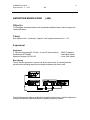
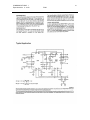
DESIGN OF A RESISTIVE ATTENUATOR
Objective
To design and test a T-type or π-type attenuator which gives an insertion loss as
required by the lab instructor while maintaining 50Ω matching at input and output.
Theory
A purely resistive circuit used to lower signal levels between a source and a load is
called an 'attenuator pad'. It does not introduce any phase shift. The pad usually also
provides input and output matching,
If low-loss impedance matching is required, matching circuits containing only reactive
components are used.
See Reference 1, class text, Chapter 1.2, for discussion of insertion loss, attenuators
and matching pads.
Figure 1
Assuming RS = RL , and the system being matched, the insertion loss is given by
V
InsertionL oss = −20 log 10 O
V IN
dB
(eq. 1)
Experiment
Equipment
DC Power Supply
Function Generator
DMM with manual
2 - 50Ω resistors (49.9Ω)
1 - prefab attenuator
1 - breadboard
1 - BNCm -banana adapter
1 - BNCm -BNCm cable
1 - Yellow grabber cable
COMMUNICATIONS 1
Experiment No. 1 - 2133
7
Attenuator
Design of the Attenuator
The lab technologist will specify the type (T or Pi) and the desired insertion loss.
Calculate the resistor values to build a symmetrical attenuator with input and output
impedances of 50Ω (see class text Fig. 1.2.2 and 1.2.3 respectively).
Choose single resistors with nominal resistances closest to the calculated values and
construct the pad.
DC Test
Set the DC Power Supply to 2V and apply directly to the input of the attenuator. Measure
the output and compute the insertion loss. Is the result what you expected?
The attenuator was designed with an input impedance of 50Ω and an output impedance of the
same value. The internal resistance of the power supply, however, is considerably less than
50Ω and the input resistance of the DMM considerably more than that. Thus, the power supply
and the DMM need to be matched to the attenuator pad!
Do the matching, and again measure the voltage at the attenuator input and attenuator
output. Adjust the power supply voltage if necessary to keep the voltage at the
attenuator input at 2V.
Compute the insertion loss.
AC Test
Disconnect the DC power supply!
Set the Function Generator to a sine wave, 2VRMS, 1 kHz output (use the DMM to
measure all voltage levels!)
Measure the insertion loss applying similar techniques as above.
With regard to the matching, consider the following:
a) the generator has an output impedance of 50Ω.
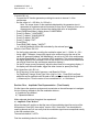
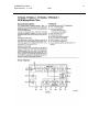
b) the following excerpt from the function generator's User's Manual:
The HP 33120A generator has a fixed output source resistance of 50Ω (see Fig.2). During
calibration, output amplitudes are calibrated for both the open-circuit voltage (no load) and the
terminated output voltage (loaded). The terminated output amplitude is calibrated for an exact
50Ω load. Since the function generator's output resistance and the load resistance form a
voltage divider, the measured output voltage of the function generator will vary with load
resistance value and accuracy. Thus, for example, if the function generator's output is
measured with no load connected, the output will be approximately twice the displayed
amplitude (V GEN instead VLOAD ).
Repeat the measurement at 10 kHz, 100 kHz, and 1 MHz.
If your measurements don't come out as expected you might want to consider a look
at the specifications in the DMM's User Manual.
Figure 2
COMMUNICATIONS 1
Experiment No. 1 - 2133
8
Attenuator
Unknown attenuator
Re-adjust the frequency to 1 kHz.
Note the number of the ready-made attenuator provided by the lab technologist.
Also record the type (T or π) and the resistor values.
Measure the insertion loss, using the same method as in the AC Test. If there is any
matching required, do so.
Make a complete sketch of your measuring circuit!
Analysis
1.
2a.
2b.
3a.
3b.
4.
Using the chosen resistor values of your attenuator design, re-calculate the new
(actual) insertion loss.
For the DC test, compare the measured to this actual Insertion Loss.
Show how you matched the dc power supply and the DMM to the pad's input and
output respectively (sketch!), and state your reasoning.
Show at which points of the complete circuit you measured VIN and VOUT!
For the AC test, compare the measured to the actual Insertion Loss (as in 2a).
Again, show what you did about the matching problem (sketch).
Using the resistor values you noted from the 'unknown' attenuator pad, calculate the
I.L. and compare with your measurement.
Questions
5. For the attenuator you designed, show that the resistance seen by the source (looking
forward into the pad) is actually 50Ω, and the resistance seen by the load (looking
back into the pad) is also 50Ω, i.e. in- and output are matched as intended.
6. If the 50Ω resistor used to match the DC supply to the attenuator input were not
provided, could the output/input voltage ratio still appear to be correct?
If so, would the measurement be correct considering the conditions stated above at
the beginning of the experiment (objective)? Prove your findings!
7. Comment on Questions 5 and 6.
8. Looking at the results of the AC test, are any of the measurements at 10 kHz, 100
kHz, and 1 MHz, off the expected value by more than 10%? If so, would you have an
explanation? Is there anything to be learned from this?
Conclusions
Comment on your experiment.
COMMUNICATIONS 1
Experiment No. 2 - 2133
9
Waveform Analysis
PERIODIC WAVEFORM ANALYSIS
Objective
To measure the Frequency Spectra for various periodic voltage-time functions, and to
compare measured results with theory.
Theory
See Reference No. 1, Class text, Chapters 2.1-2.9.
Study in particular eqs. (2.7.1), (2.9.1), (2.9.2), (2.9.3), (2.9.4), and the associated
diagrams.
The oscilloscope is by far the most common used instrument to analyze signals in the
time domain (i.e. representation of signal amplitude versus time). However, the analysis
of signals in the frequency domain (i.e. the representation of signal amplitude versus
frequency) requires the use of a group of instruments called analyzers, the most
versatile of this group being the Spectrum Analyzer.
In this experiment we will use the spectrum analyzer to find the harmonics of the
investigated waveforms. The oscilloscope serves only to observe the proper waveform
selection, but is not used to make measurements.
Experiment
Equipment
Function Generator HP 33120A
Oscilloscope Fluke PM 3370B or HP 54645D
Spectrum Analyzer HP E4411B
DMM Fluke 45
50Ω resistor
BNC-banana adapter
BNCF to BNC F adapter
BNC-T adapter
1 BNC cable, short
1 BNC cable, long
For students not familiar with the instruments, the following notation may help with the
use of the instruments:
[Function Keys]
= Labeled Keys
<Menu Keys>
= Unlabeled Soft Keys
COMMUNICATIONS 1
Experiment No. 2 - 2133
10
Waveform Analysis
A. Sine Wave
We start out with the most straight forward waveform, to get acquainted with the
spectrum analyzer.
LINEAR MEASUREMENT
Set the Function Generator to [Sine], [Frequ] = 100 kHz, [Amp] = 200 mVP-P .
To set up the desired waveform properly we need to pay attention to the generator's
output matching requirements (remember Exp. #1, Fig. 2).
a-1) Connect the signal to the oscilloscope. Does it correspond to what the function
generator's display indicates? Record!
a-2) Connect the signal to the DMM. Measure on the DC range and on the AC range. Do
these measured data correspond to the generator's display? Record!
dB MEASUREMENT
Connect the signal to the Spectrum Analyzer.
Set the Spectrum Analyzer as follows:
[Frequency], <Start frequency> = 0 kHz (press 0 on numeric pad, then <kHz>)
<Stop frequency> = 1 MHz
[Span],
Should read 1MHz, i.e. horizontal base is 100 kHz/division
[Amplitude], <Ref Level> = 100 mV (press 100 on numeric pad, then <mV>)
<Scale Type> = 'Lin'
The bottom scale now reads frequency from 0 Hz to 1 MHz, i.e. 100 kHz/div.
The left (vertical) scale now reads from the Ref.level = 100mV on the top to 0 V at the
bottom, i.e. 10mV/division.
a-3) Close to the left end of the frequency scale, at f = 100 kHz, the analyzer shows the
amplitude of the fundamental (or 1st harmonic) frequency component.
Measure this amplitude.
Note:
the spectrum analyzer input impedance is 50Ω
the spectrum analyzer displays the RMS-value!
Check the amplitude of this frequency component: does it correspond to the value
you expect to see? Is it correct? Record!
Compare with the function generator's output display. Does everything make
sense? Note!
COMMUNICATIONS 1
Experiment No. 2 - 2133
11
Waveform Analysis
B. Square Wave
Now, on the function generator, switch to [square wave].
LINEAR MEASUREMENT
The set-up is the same as for the sine wave. Now,
b-1) On the spectrum analyzer, read and record the amplitudes of the fundamental and
the harmonics up to the 9th harmonic.
For this measurement, you may like to use the 'Peak Search' function: Press
[Peak Search], then <Next Right>, etc. (Some analyzers have only 'Search'
printed on the button, but the function is the same).
dB MEASUREMENT
Normally, spectrum analyzer measurements are NOT done using a linear display as
shown above, but rather using a logarithmic scale to increase the dynamic range.
Amplitudes are displayed in dBm (this is a power measurement, displayed in dB with
reference to 1mW), and the differences between amplitudes (power levels) can be read
directly in dB.
To get familiar with this type of measurement, we repeat the experiment using the dB
display.
Press [Marker] and <Off> to clear all markers from the screen.
Press [Amplitude] and change from <Lin> to <Log>. Amplitudes are now displayed in
dBm.
If not already there, press <Ref Level> and move the peak of the fundamental or 1st
harmonic to the top graticule line by turning the knob. The fundamental is now the
reference against which all other harmonics are measured.
Since we know by now from the linear measurements of the square wave spectrum that
only odd harmonics exist, move the marker - using the [Peak Search], <Next Pk right>
routine - to the (frequency) location of the 3rd harmonic: The difference of the power
level indicated now to the level measured for the fundamental shows how much the
power level of the 3rd harmonic is below the level of the fundamental spectral
component. The difference is measured in dB.
b-2) Using the approach just described, measure the power levels of the fundamental
and the harmonics up to the 9th.
Incidentally, a more convenient way of measuring the above is to set the
fundamental as 0-dBm reference and read the harmonic's power levels
directly. To do this, press [Peak Search]: the marker jumps to the highest
peak. Then press [Marker] and <Delta>. This sets the level of the marker (at
the fundamental) at 0 dB, and using the [Peak Search], <Next Pk right>
routine allows to quite easily read the levels of the other harmonics directly
with reference to the fundamental.
Note: the Delta function also sets the frequency of the fundamental to Zero –
ignore since this is obviously not the case!
If you would like to save the screen display of the analyzer on disk, see Appendix A.
COMMUNICATIONS 1
Experiment No. 2 - 2133
12
Waveform Analysis
C. Pulse Train Wave
Disconnect the spectrum analyzer and press the green [Preset] button. The spectrum
analyzer switches back to its default values.
The set up is the same as for the previous measurements. Again, pay attention to the
generator's output matching requirements.
Assuming that we still have the square set up from the previous experiment, adjust the
[Amplitude] to 350mVpp and [Offset] to +175 mV dc. The oscilloscope should display the
bottom of the square wave to be on the GND level.
Now change the duty cycle to set the pulse waveform: [Shift] [% Duty], set to 20%
[Enter].
This waveform has a dc spectral component which, too, has to be measured. For this
you use the DMM.
Observing the oscilloscope and the DMM, check whether the displays show exactly what
you expect them to show. If you are satisfied, go ahead with your measurements. If you
are not satisfied, think what could be wrong and what could be done to remedy the
problem. Remember the function generator's output characteristics...
Once everything is all right,
c-1) record the dc component
Then remove all present connections and connect the function generator directly to the
spectrum analyzer.
Set the spectrum analyzer up similar as in part A, with the Start frequency at 0 Hz and
the Stop frequency at 1 MHz. The frequency scale now reads from 0 Hz to 1 MHz with
100 kHz/div.
LINEAR MEASUREMENT
c-2) Measure the spectrum similar as done for the square wave (linear display), up to
the 10th harmonic.
The analyzer's 'Peak Search' function may not mark very small components
(smaller than about half a division). To get a measurement for these use the knob
to move the marker or estimate directly from the screen.
dB MEASUREMENT
c-3) Measure the spectrum similar as done for the square wave (log display), up to the
10th harmonic.
COMMUNICATIONS 1
Experiment No. 2 - 2133
13
Waveform Analysis
Analysis
1. For both waveforms, compute the amplitudes of the fundamental and the harmonic
frequency components, in the linear mode. Do the same for the log (dB) mode, but
this time find the amplitude of the higher harmonics with reference to the fundamental,
i.e. setting the fundamental to 0 dB and for the other harmonics find the difference to
the fundamental in dB
Show at least one sample calculation for each waveform!
Don't forget the dc component.
2. Present both the measured and the computed data in tables for comparison.
3. Sketch the frequency spectrum for both waveforms on graph paper to scale, linear
amplitude of each frequency component vs. frequency, for the number of harmonics
measured. Use single lines to represent the frequency components.
Questions
4. When you did the measurements for the Square Wave using the Log-scale,
the display most likely indicated the presence of harmonics not only at the odd
frequency locations, but also at the locations of the even harmonics, though at
a much lower level. What could be the cause of that, and is this acceptable?
Consider the power level of these even harmonics shown by the analyzer, and
also compare with the linear display!
5. Consider a common telephone channel with the bandwidth limited from 300 Hz
to 3400 Hz by a n ideal band pass filter. You apply a square wave of 400 Hz
and1V amplitude to the input. At the output of this filter, what would
a) the signal waveform approximately look like (time domain)? Sketch!
b) the spectrum look like (frequency domain)? Sketch!
Conclusions
Comment on your results.
COMMUNICATIONS 1
Experiment No. 3 - 2133
AMPLITUDE MODULATION
14
AM
( AM )
Objective
To investigate the characteristics of an amplitude-modulated wave, and to compare the
results with theory.
Theory
See reference No.1, (class text), chapter 8, and in particular sections 8.1 - 8.5.
Experiment
Equipment
2 Function Generators HP 33120A (or one HP and one other)
Oscilloscope HP 54645D
Spectrum Analyzer HP E4411B
2 BNC T-adapters
2 short BNC cables
2 med. BNC cables
Basic Set-up
The HP function generator is used to set up the carrier wave. A second generator
provides the modulating signal and externally modulates the carrier wave.
The Oscilloscope provides an amplitude-time display (time domain), while the Spectrum
Analyzer provides an amplitude-frequency display (frequency domain).
COMMUNICATIONS 1
Experiment No. 3 - 2133
15
AM
CARRIER SET-UP
- Connect the HP function generator providing the carrier to channel 1 of the
oscilloscope.
- Set the carrier to f = 300 kHz, A = 200 mVP-P.
Note: The scope shows 2x the amplitude displayed by the generator since it
represents an impedance almost equivalent to open circuit. However, this is of no
consequence in this case, because we dealing with ratios of amplitudes.
- Press [Shift][Recall Menu], display shows "A:MOD MENU
- Press [ω], display: "1:AM SHAPE"
- Press [>], display: "2:AM SOURCE"
- Press [ω], display: "EXT/INT"
- Press [>], display: "EXT"
- Press [Enter]
- Press [Shift] [AM], display: "AM,EXT"
i.e., now the generator will be AM-modulated by the external input only.
M ODULATING SIGNAL SET-UP
- On the function generator providing the modulation signal, set f = 10 kHz, A = 2VP-P.
- Using a BNC T-adapter, connect this signal to the external input at the rear of the
carrier HP generator (labeled "AM Modulation") as well as to CH2 of the oscilloscope.
(An external amplitude of ~5Vp-p provides 100% modulation. The actual amplitude of
the signal applied to the modulator circuit of the carrier is of course much smaller and
can only be found from the oscilloscope waveform displays.)
- On the HP scope, press [Autoscale], adjust the time base for a convenient display. If
the display can't be made stable, trigger the other channel or press [Run/Stop].
SPECTRUM ANALYZER SET-UP
- Set [Frequency] to the carrier frequency and [Span] to 50 kHz.
- On [Amplitude], change 'Scale Type' from <Log> to <Lin>. Press [Ref Level] and
adjust the carrier amplitude until the peak of the carrier just reaches the top graticule
(= reference) line. Thus the carrier is now normalized to 1, or 10 divisions.
Section One : Amplitude-Time Representation (Time Domain)
We first ignore the spectrum analyzer and concentrate on the oscilloscope to investigate
the two common methods to find the modulation index m:
a) Amplitude-Time Method
b) Trapezoidal Method
Make adequate sketches throughout the experiment!
a) Amplitude -Time Method
Move the channel 2 position so that the trace of the modulating signal lies on top of the
AM-envelope. Press [A2], then switch 'Vernier <ON>'. Now trace 2 can be adjusted in
small increments and you can verify that the modulation signal trace corresponds exactly
to the AM envelope trace.
Then switch channel 2 <OFF>.
Find the modulating index for the following conditions:
COMMUNICATIONS 1
Experiment No. 3 - 2133
16
AM
a-1) Set the amplitude of the modulating generator to 1VP-P, sinusoidal waveform.
- record the amplitude of the carrier in VP-P from the scope display by temporarily
disconnecting the modulation signal (if the display is unstable change trigger to
channel 1 by pressing [Edge] and <A1>
- record the amplitude of the modulating signal in VP -P from the scope display (not
from the modulating generator display!)
- make sketches of the waveforms, indicating your measurements
a-2) Set the amplitude of the modulating generator to 2VP-P and change the modulating
signal to a square wave.
- repeat the measurements as in a-1.
a-3) Set the amplitude of the modulating generator to 3VP-P and change the modulating
signal to a triangular wave.
- repeat the measurements as in a-1.
a-4) Set the amplitude of the modulating generator to 4VP-P and change the modulating
signal to a ramp wave.
- repeat the measurements as in a-1.
a-5) Set the amplitude of the modulating generator to 5VP-P and change the modulating
signal back to a sine wave. If over-modulation occurs, lower the amplitude so that
100% modulation is achieved (i.e. the upper and lower envelopes just touch)
- repeat the measurements as in a-1.
b) Trapezoidal Method
On the oscilloscope, clear all cursors, switch Ch2 'on' and adjust the scale to observe
the modulating signal.
To see the trapezoidal display,
- On the HP scope, exchange CH1 and CH2 connections, press [Autoscale],
[Main/Delayed], then <XY>
b-1) For the same conditions as stated in a-1, use eq. 8.3.2 class text to find m.
The size of the trapezoidal display can be changed for better viewing by varying
the vertical deflection of Ch1 and Ch2.
Make sketches as above.
b-2) through b-5)
Repeat this measurement under the same conditions as given in a-2 through a-5.
When finished, go back to the amplitude-time display:
- On the HP scope, clear cursors, press [Main/Delayed], then <Main>. Change time
base for convenient display and if necessary adjust the trigger : [edge], <A1>
Section Two : Amplitude-Frequency Representation (Frequency Domain)
Make adequate sketches throughout the experiment!
Now concentrate on the Spectrum Analyzer. Begin with the <Lin> display.
What you see there now is the amplitude spectrum for a sinusoidally modulated carrier
wave, as shown in Fig. 8.5.1, class text.
Set [Span] back to 100 kHz , and the modulating generator to the sine wave form.
The following measurements are for sine wave only.
COMMUNICATIONS 1
Experiment No. 3 - 2133
17
AM
Remove the modulation (disconnect the modulating generator) and observe the carrier
on the screen: re-adjust the peak of the carrier to the top graticule line if necessary,
turning the knob slowly (and waiting a second or two until the analyzer has caught up
with the new level).
Now the carrier can be considered normalized to 1, scaled to 10 divisions.
c-1) Re-connect the modulating signal and set it to 2VP -P.
Record the amplitude of the side frequencies, in terms of % or divisions of the
unmodulated carrier.
c-2) Set the modulating signal to 3.5VP-P and repeat the measurement as in c-1.
c-3) Set the modulating signal to 5VP- P and repeat the measurement as in c-1.
c-4) Change display from 'Lin' to 'Log'. The carrier should be at the top graticule line.
For the same conditions as in c-1 through c-3, measure and note the amplitude
level of the sidebands relative to the carrier (in dB).
(How? Remember Experiment No. 2)
Section Three : Application
Record the inventory number on the top front edge of spectrum analyzer (EA-xx)!
Disconnect the input cable to the spectrum analyzer.
Press [Preset] to put the analyzer in its default condition.
Press [File], then <Load>, then <Trace>.
Drive C: should be highlighted.
Turn knob to highlight the filename. In our case, the desired filename for 2nd year
students is "AM2", for 3rd year students "AM3". Record the filename you used !
Press [Enter]
From the display, record
d-1) center frequency
d-2) span
d-3) positions (frequencies) of the lower and upper side frequency
d-4) scale type (Lin or Log)
d-5) with the carrier set to reference (= top) line, record the amplitudes of the side
frequencies with reference to the carrier
Analysis
1. Collect all data in a suitable form in a clearly arranged table.
2. Section One, part a), amplitude-time method:
Using eq. 8.3.1. class text, find the modulating index m for the given modulating
conditions a-1 to a-5. Show how you did that (sketches, sample calculation)
COMMUNICATIONS 1
Experiment No. 3 - 2133
18
AM
3. Section One, part b), trapezoidal method:
Using eq. 8.3.2 class text, find m for the given modulating conditions b-1 to b-5. Show
how you did that (sketches, sample calculation)
4. Section Two:
Using eq. 8.5.1 class text, find m for the given modulating conditions c-1 to c-3 ('Lin'display). Show a sample calculation and sketch the spectrum.
5. Section Two:
Show the relation of the side frequencies to the carrier, with the carrier set to 0 dB as
the reference, i.e. the difference in dB ('Log'-display) between side frequencies and
carrier. Show a sample calculation and sketch the spectrum.
6. Section Three:
From the recorded data, find
carrier frequency fC ,
modulating signal frequency f M,
modulating index m,
bandwidth
Conclusions
Comment on differences, advantages and disadvantages of the amplitude-time and
the trapezoidal method
Questions
1. To control an AM radio station's signals, which type of measuring method,
amplitude-time or trapezoidal, would you use to monitor m, and why?
2. If an amplitude-modulated carrier of amplitude 1V is set at 1 MHz and the
function generator supplying the modulating signal would be swept with a
sinusoidal signal over a range of 2 kHz to 20 kHz and m=60%, what would
a) the linear spectrum look like (sketch, with amplitude to scale)?
b) the bandwidth be?
.
COMMUNICATIONS 1
Experiment No. 4 - 2133
FREQUENCY MODULATION
19
FM
( FM )
Objective
To study some aspects of frequency modulation.
Background
Compared to amplitude modulation, frequency modulation provides enhanced noise
performance, i.e. a better signal-to-noise ratio, at the expense of increased bandwidth.
Together with amplitude modulation, FM is one of the classic modulation techniques.
Theory
See Reference No.1, class text, Chapter 10, sections 10.1 - 10.5.
Experiment
Equipment
Function Generator HP 33120A
Oscilloscope HP 54645D
Spectrum Analyzer HP E4411B
Notations and formulas used
Carrier frequency
fC
Modulating frequency
fM
Frequency deviation
∆f
Modulation Index
β
Bandwidth
BFM
BNC T-adapter
2 short BNC cables
COMMUNICATIONS 1
Experiment No. 4 - 2133
Modulation Index
Bandwidth
20
FM
β=
∆f
fM
BFM = 2(∆f + f M )
(Eq. 4-1)
(Eq. 4-2)
Eq. 4-2 is known as Carson's Rule. The occupied bandwidth is usually considered using
the side frequencies larger than 1% of the unmodulated carrier (as a guideline).
FM Spectrum
Set the function generator up as follows:
carrier frequency
fC = 100 kHz
carrier amplitude
A = 200 mVP-P
select [Shift][FM]
modulating signal frequency
fM = 10 kHz
max. deviation
∆f = 5 kHz
Observe the resulting waveform on the oscilloscope (try time base 20µs). It is not all that
informative, but at least gives an impression what a frequency modulated signal looks
like.
However, we are more interested in the frequency spectrum. Thus, the spectrum
analyzer is the instrument exclusively used for our measurements in this experiment.
A) Amplitude level measurements
On the Spectrum analyzer, set
[Frequency] <center frequency> to fC ,
[Span] to a suitable range
[Amplitude] to <Lin>
On the generator, press [Shift] [FM], to switch the modulation off. The scope now shows
the unmodulated carrier.
On the spectrum analyzer, press <Ref Level> and adjust the carrier peak to the top
graticule (= reference) line. This corresponds to the amplitude of the unmodulated
carrier's spectrum being normalized to 1, over 10 vertical divisions.
a-1) With ∆f still set to 5 kHz, switch the modulation on again and record the
amplitudes of the sinusoidal spectrum components of the modulated carrier and
the side frequencies, with the normalized carrier as reference. (In practical terms,
measure the divisions: a side frequency with an amplitude of for example 3
divisions equals 0.3 x the carrier amplitude).
It is sufficient to record only the significant side frequencies. (Consider significant
side frequencies as those with an amplitude of 1% or more of the unmodulated
carrier amplitude).
Record the positions of the side frequencies on the frequency scale with regard to
the carrier, that is, the distance of the side frequencies to the carrier frequency.
a-2) Change the deviation to ∆f = 24 kHz.
Repeat the above measurements (you may want to change Span to a more
convenient value to accommodate all significant side frequencies).
COMMUNICATIONS 1
Experiment No. 4 - 2133
21
FM
a-3) Change the deviation to ∆f = 40 kHz.
Repeat the above measurements, again changing Span if necessary.
B) Power level measurements
On the spectrum analyzer [Amplitude] menu, switch from <Lin> to <Log>.
Switch FM off again and verify that the unmodulated carrier aligns to the top graticule
line as the reference level.
Press [Marker] and <Delta>. This sets the carrier reference to 0 dBm and allows the
difference of the amplitudes of the side frequencies to the amplitude of the unmodulated
carrier conveniently to be recorded in dB. The [Peak Search] or [Search] function may
be useful, too.
Switch FM on again and for the same number of side frequencies as seen on the linear
display, or seen on the Bessel's table, record the levels of the sinusoidal spectrum
components with reference to the unmodulated carrier (i.e. the difference) in dB :
b-1) Do these measurements under the same modulation conditions as done in a-1.
b-2) Repeat the measurements with the same modulation conditions as in a-2.
b-3) Repeat the measurements with the same modulation conditions as in a-3.
C) Deviation
As on the oscilloscope, the deviation of a carrier is not readily observed on the spectrum
analyzer (switch to linear display) under realistic modulation conditions. For the purpose
of demonstration only, set up conditions as follows:
fC
fM
∆f
span
= 100 kHz
= 0.1 Hz (100 mHz)
= 10 kHz
= 100 kHz
Switch the FM modulation off. Note the position of the carrier.
Switch the FM modulation on again. Make notes of what is happening.
Change fM to 0.2 Hz, then to 0.3 Hz. Make notes of observations.
Change ∆f to 20 kHz, then to 30 kHz. Make notes of observations.
D) Bandwidth
We now have a look at the bandwidth occupied by the spectrum. We set up a carrier and
modulate it with various modulating signal frequencies while keeping the deviation
constant.
Take all [Markers] <Off>.
Set fC = 500 kHz, amplitude = 200 mVP-P
∆f = 75 kHz
Center frequency to fC
Span to 200 kHz
Amplitude to <Lin>
Ref level to 10 mV
COMMUNICATIONS 1
Experiment No. 4 - 2133
22
FM
d-1) Set fM = 100 Hz
Measure the approximate bandwidth. Easiest way to do this:
Press [BW/Avg], change <Resolution Bandwidth> from <Auto> to <Man>. Then
turn knob to set resolution bandwidth to 1 kHz.
Press [Marker], <Span Pair>, then set to <Span>. Turning the knob symmetrically
moves two markers and the frequency difference (bandwidth) can be read directly
off the screen.
d-2) Set fM = 1 kHz
Repeat the above measurement.
d-3) Set fM = 10 kHz
Repeat the above measurement. Change [Span] if necessary.
E) Application
Record the inventory number on the top front edge of the spectrum analyzer (EA-xx)!
Disconnect the signal input from the spectrum analyzer.
Load a file:
Press [Preset] to put the analyzer into the default state.
Press [File] and <Load>, then <Trace>
Drive C: should be highlighted. If not, change to C: with <Select> function
Turn knob to select the filename. In this case the desired filename for 2nd year
students is "FM2", and for 3rd year students "FM3". Record the filename you used!
Then press [Enter].
The file should be loaded and the screen should show some spectrum.
Record carrier and side frequency amplitude levels and the spectrum component's
frequency locations, i.e. the complete spectrum (assume the unmodulated carrier level
was set to the top graticule line as reference)
Record also center frequency and span.
Bessel's table:
Mod Index
β
0.25
0.5
1.0
1.5
2.0
2.4
3.0
4.0
Carrier
J0
Side Frequencies
J1
J2
0.98
0.94
0.77
0.51
0.22
0
− 0.26
− 0.40
0.12
0.24
0.44
0.56
0.58
0.52
0.34
− 0.07
0.01
0.03
0.11
0.23
0.35
0.43
0.49
0.36
J3
J4
0.02
0.06
0.13
0.20
0.31
0.43
0.01
0.03
0.06
0.13
0.28
J5
J6
J7
0.02
0.05
0.02
Un-modulated
carrier
amplitude
= 1.0
0.01
0.05
0.13
Negative values are of mathematical interest only. For the modulation always use the absolute
value, of course.
COMMUNICATIONS 1
Experiment No. 4 - 2133
23
FM
Analysis
Part A
- For the modulating conditions given in a-1 through a-3, find the modulating index β
from the Bessel's table.
- From the Bessel Functions table, which lists the amplitude coefficients of the
modulated carrier and the side frequencies with regard to a normalized carrier, find
the theoretical amplitude levels corresponding to your measurements.
- Neatly tabulate the experimental together with the theoretical data for convenient
comparison.
Part B
- Similarly to part A, show the results in terms of dB.
Part C
- Interpret your observations.
Part D
- For the given modulating conditions, compute the bandwidth of the occupied
spectrum using Carson's Rule.
- Compare your experimental data with the computed data.
- With regard to part D, how closely do the measured bandwidth and the
bandwidth given by Carson's Rule correlate? What conc lusion would you
draw from these results with regard to the validity of Carson's Rule?
- Consider the same variation of f M as in part D applied to an AM signal. How
does it affect the bandwidth here, compared to FM?
Part E
- From your recorded data, find fC , fM, ∆f and β.
Conclusions
Comment on the experiment and your results.
COMMUNICATIONS 1
Experiment No. 5 - 2133
PULSE CODE MODULATION
24
PCM
( PCM )
Objective
To investigate aspects of quantization, synchronization, companding and multiplexing
processes in a PCM system.
Background
To make use of the many advantages of transmitting digital signals over transmitting
analog signals (speed, precision, security etc.), a number of schemes are available to
modulate a pulse train with the desired information.
The most important of these methods is Pulse Code Modulation where an analog signal
is sampled and "translated" into a binary signal consisting of strings of a fixed number of
On- or Off-states.
Theory
See Reference No.1, class text, Chapter 11.1-11.3 (sections about quantization,
compression and receiver).
For more detailed information regarding this particular circuit see the the following
outline, schematics and the attached extract from the manufacturer's data book.
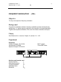
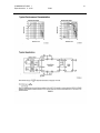
Experiment
System Description
Read the description and details presented in the specification sheets and study the
circuits. The board layout on (Fig.1) should help you find your way through the
experiment.
Condensed Outline
The system is provided on a PC board and self-contained except for a power supply and
measuring equipment. The actual system consists mainly of two ICs, a CODEC
(COder/DECoder) and an IC containing filters. Both are designed by the manufacturer to
work together as a unit. One set handles both the transmission (coding) as well as the
reception (decoding).
The analog signal enters the board at AIN and passes through a filter via a switch into the
CODEC. The switch allows a DC voltage (also provided on the board) to enter the
CODEC instead of the analog signal. The CODEC samples the incoming signal at a rate
of 8 kHz, assigns an 8-bit digital number to the sampled level and shifts this number out
COMMUNICATIONS 1
Experiment No. 5 - 2133
25
PCM
to be transmitted via PCMTX. In our case, the signal is looped right back. The signal
received at PCMR X, i.e. the received digital bit stream, is decoded by the CODEC,
resulting in a sort of stepped waveform, the steps corresponding to the received pulse
sequence. This waveform is passed through a filter to smoothen out the steps and now,
representing the original signal, is finally available at AOUT.
The CODEC may be used in multiplexed systems. Each CODEC can handle one out of
32 available channels of 8 bits each. The 32 channels times 8 bits each make up one
frame. A frame synchronizing pulse derived from the system clock marks the start of a
new frame. As mentioned above, one digital word is 8 bits long.
As mentioned above, one of 32 channels (called time slots in the specs) can be
assigned to one CODEC (see the table in the attached codec spec sheet). Each CODEC
has to be programmed to assign a time slot for its channel, and in which mode the
CODEC is to be operated in this slot, i.e. to encode, decode, do both or to be powered
down. A programmer circuit designed for this purpose is integrated on the board. The
desired time slot and mode is set with a multi-switch. Pressing the time slot programmer
pulse TS push button switch sends control clock pulses and an 8-bit series of control
data pulses to the CODEC initiating the assignment. The whole process is controlled by
the frame synchronizing pulse FS occurring at an 8 kHz rate.
Procedure
Equipment:
PC-board
Power Supply
Oscilloscope
DMM
Function Generator
Use the 10x probes with the oscilloscope at all times.
Make notes and sketches of your observations throughout the experiment!
This is important since it will help to clarify the various concepts encountered in the
experiment, which simulates a telephone link as it is used today.
1. Set-Up
The CODEC handles transmitting AND receiving at the same time. We use this feature
by feeding our transmitted PCM right back to be received again. This allows an easy
comparison of the outgoing and the received signal.
Therefore, set the mini switches to assign the time slot mode to "Encoder and Decoder"
(B1 = 0, B2 = 0), and to time slot 1 (B3 . . . B8 = 0). Note that setting a "0" in this circuit is
to set the switch to "ON" (IC 15, Fig. 4).
If not already in place, set the jumper-shunts to 'AIN and 'Not Signalling'.
COMMUNICATIONS 1
Experiment No. 5 - 2133
26
PCM
Apply a sine wave approximately 2 kHz to the 'AIN ' BNC-input, with an amplitude of
350mVP-P measured at TP2 (remember: the scope probes are 10x). This provides a
signal of approx. 2 VP-P applied to the CODEC input.
2. Signal path trough the system
To get an overlook of the whole system, follow a signal applied to the input through the
whole system until received and re-constructed at the output:
Connect CH1 probe to AIN (TP1). Trigger the oscilloscope on CH1 and adjust the time
base to observe the incoming signal.
Connect the CH2 probe to TP2, showing the signal after the filter. It is unchanged except
for the amplitude since the filter provides some amplification. This (analog) signal enters
now the CODEC.
Unfortunately, nothing can bee seen of the intermediate steps applied to the signal by
the CODEC (quantization, pulse amplitude modulation, etc.), until the PCM pulse train
appears at the output at PCMTX (TP4). The output looks somewhat strange, but we will
have a closer look at that shortly.
Feeding this signal back into the receiver part of the CODEC, the output of the CODEC
shows the decoded signal at TP6. The waveform on the oscilloscope may not look like
much of the original signal yet. On the function generator, change the frequency to
approx. 300 Hz, adjust the trigger and Hold Off to get a stable display. The waveform
can now readily be observed and reminds the observer of a staircase shape. This shows
clearly how the CODEC now performs the reverse procedure of quantizing, assigning a
discrete voltage level to each particular 8-bit number or sequence.
Connect the other probe to AOUT (TP7). The original signal is reconstructed, showing a
fairly clean sine wave after passing trough the filter, and also some amplification with
regard to the input signal.
Change the frequency back to the previous value
3. FS-Puls
Connect CH1 probe to the Frame Synchronizing pulse (TP3). Adjust V/div to see the
pulse, and expand the time base so that the pulse is approximately 1 division in length.
Connect CH2 probe to the transmitted PCMTX (TP4). You will see then a particular
pattern on the scope screen, consisting of an upper trace (1-level) and a lower trace (0level). You may have to adjust V/div to observe this properly. Turning the intensity fully
clockwise you can also distinguish clearly a set of 8 bits, representing a binary number
related to voltage level at the sampling moment. Of course, since the sine wave level
changes continuously, the eye is unable to follow this at a 8 kHz rate and perceives to
see all 8 bits at the same time.
Temporarily connect CH2 probe to the system clock (TP10) and compare the clock
period to
a) the width of the FS-pulse (TP3), and
b) the width of one bit of the PCM-Signal (TP4)
COMMUNICATIONS 1
Experiment No. 5 - 2133
27
PCM
Since the FS-pulse synchronizes the whole system time-wise, this pulse lends itself as
the best trigger source for most measurements on the scope.
4. PCM Signal
Under procedure No. 3, it has been observed that the PCM signal consists of an 8-bit
sequence for a certain voltage level, but because of the time varying nature of the
applied sine wave the value of any single bit (1 or 0) cannot be observed.
If we want to have a closer look at the PCM signal we therefore need to find some
special arrangement to "slow things down".
To see the PCM sequence for a particular voltage level would require the continuous
sampling of the same level, thus encoding the same 8-bit 'word' or number every time.
This can be done using a little "trick" by applying a variable DC source as the input
signal. Then the sampled signal level can be left constant or be changed in any desired
interval or step and the 0- or 1-value of each bit of the 8-bit number (sequence)
representing this level can be observed on the screen.
Set all mini switches B1 . . . .B8 to "0" (On), i.e. assign time slot 1.
Change the jumper from AIN to EXT DC IN. The DC voltage level can be monitored on
the voltmeter and should cover the same range as the peak-peak AC signal, that is +/2VDC . Like the AC signal before, the DC voltage is now applied to the CODEC input.
Trigger on CH1 (FS-pulse). Adjust the time base to display the FS-pulse, with a width of
one division.
Connect Ch2 probe to PCMTX (TP4). Turn the DC control (on the board) and you can
now see the 8 bits taking values of 0 or 1, depending on the DC voltage level.
Since with this time base setting 1 bit is approximately 1 division wide, it is easy to read
the 8-bit sequence. The falling edge of the FS-pulse marks the beginning of the first bit
(the MSB; the LSB is the one at the right end).
5. Time Slot
The 8-bit sequence represents the first of 32 time slots (= channels) available. Other
time slots may be assigned using the table provided in the spec sheet of the CODEC
making it possible to run 32 CODECs or 32 lines at one time (Multiplexing).
(See the table on the CODEC spec sheet).
Decrease the time base until you can see one complete frame (i.e. two FS-pulses). The
8-bit sequence or number is now 'squashed' together bit still quite distinguishable, and
representing time slot 1.
Set the mini switch B8 to "1" (i.e. to "Off").
COMMUNICATIONS 1
Experiment No. 5 - 2133
28
PCM
Pressing the TS-button initiates the assignment of the new time slot. On the screen you
see the 8-bit sequence move to the right, into the second time slot.
Setting B7= 1, B8= 0 and pressing TS moves the 8-bit number further right, to the third
time slot. Setting B7= 1, B8= 1 assigns time slot no. 4, and so on.
Setting B4 . . . B8 to "1" assigns the 32nd time slot.
Assign time slot 1. Expanding the time base again you can see that the MSB (the first bit
counting from the left) starts with the falling edge of the FS-pulse. Assign slot 32. Now
you can observe that the LSB (the 8th bit counting from the left) ends with the falling
edge of the FS-pulse.
6. Companding
To enhance the S/N-ratio of a small signal on the transmission channel a process of
COMpressing the signal before transmission and exPANDING it upon reception is
frequently being used, the combination of both thus called COMPANDING.
Instead of dividing the range from -2V to +2V into 256 equal steps for the A/D
conversion, the range is divided into segments with progressively smaller voltage
increments from ±2 V towards 0 Volts.
In our experiment we will have a close look at the compression part. We could include
the expansion part, too, but it will be omitted here due to time limitations in the lab.
Assign time slot no. 1.
Move the shorting bridge from 'AIN ' to 'Ext DC In'.
Vary the DC voltage and note the binary sequence according to the following table.
These are the minimum number of measurements, taking more readings will provide
improved results.
See table 5-1 to collect the data. The resulting curve is somewhat idealized but provides
a good perception of the principles involved.
COMMUNICATIONS 1
Experiment No. 5 - 2133
29
PCM
Table 5-1 :
VDC (IN)
[V]
Binary Sequence
MSB . . . . . . LSB
Decimal Equivalent
to the 8-bit sequence
- 2.00
- 1.80
- 1.60
- 1.50
- 1.40
- 1.20
- 1.00
- 0.80
- 0.60
- 0.50
- 0.40
- 0.33
- 0.26
- 0.20
- 0.10
~ <0
~ >0
+ 0.10
+ 0.20
+ 0.26
+ 0.33
+ 0.40
+ 0.50
+ 0.60
+ 0.80
+ 1.00
+ 1.20
+ 1.40
+ 1.50
+ 1.60
+ 1.80
+ 2.00
00001011
11
01111111
11111111
127
255
10001 011
139
Analysis
1. Describe and sketch the steps of a signal passing through the system, from input
signal to transmitted signal, from received signal to output.
2. Compare and sketch the relationship between clock pulses, FS-pulse and PCM signal
sequence.
3. Sketch a full frame showing the 32-channel organization, with respect to the FSpulse.
COMMUNICATIONS 1
Experiment No. 5 - 2133
30
PCM
4. Using your data from procedure no.6, plot Decimal Equivalent (ordinate) vs. VDC(IN)
(abscissa) on graph paper.
Note the "flip" of the binary sequence and the decimal equivalent at 0 Volts. That means
you need to adjust your ordinate scaling to accommodate a smooth transition!
The shape of the graph is the result of 'compressing', in our case according to a signal
processing scheme called 'µ-law '. When the signal is reversed it undergoes a similar
decompressing process, restoring the original form.
Conclusions
Comment on your experiment
Questions
1. What is the purpose of the input filter?
2. What is the purpose of the output filter?
3. To show the bit sequence for the companding part, we changed from an AC to
a DC signal. Why was this necessary?
4. Demonstrating on your graph of the compression process, and in your own words,
attempt a short interpretation of the purpose and effect of this feature.
COMMUNICATIONS 1
Experiment No. 5 - 2133
Fig. 1
31
PCM
COMMUNICATIONS 1
Experiment No. 5 - 2133
Fig. 2
32
PCM
COMMUNICATIONS 1
Experiment No. 5 - 2133
Fig. 3
33
PCM
COMMUNICATIONS 1
Experiment No. 5 - 2133
Fig. 4
34
PCM
COMMUNICATIONS 1
Experiment No. 5 - 2133
35
PCM
COMMUNICATIONS 1
Experiment No. 5 - 2133
36
PCM
COMMUNICATIONS 1
Experiment No. 5 - 2133
37
PCM
COMMUNICATIONS 1
Experiment No. 5 - 2133
38
PCM
COMMUNICATIONS 1
Experiment No. 5 - 2133
39
PCM
COMMUNICATIONS 1
Experiment No. 5 - 2133
40
PCM
COMMUNICATIONS 1
Experiment No. 5 - 2133
41
PCM
COMMUNICATIONS 1
Experiment No. 5 - 2133
42
PCM
COMMUNICATIONS 1
2133
43
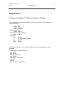
APPENDIX A
Appendix A
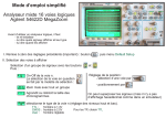
Saving screen display of the Spectrum Analyzer (bitmap)
Once the display is on the screen (either from an input waveform or loaded from the
internal hard drive),
- press [File]
- press <Save>
- press <Screen>
change destination :
- press [Tab ⇒]
choose filename, using soft keys :
press
[Tab ⇒]
choose drive :
press
<Select>
- A - should be highlighted
press
<Select>
press
[Enter]
The file is now saved on A: as a bit map (.gif) file and can be imported into a word
processor.
For example, to import into WORD,
- click 'Insert'
- click 'Object'
- click 'Create from file'
- click 'Browse'
- open drive A:, choose file
- click 'OK'
- click 'OK'
- size and move to desired spot