1
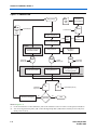
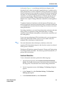
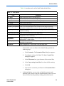
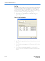
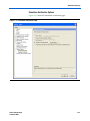
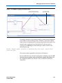
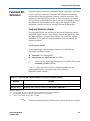
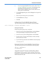
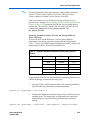
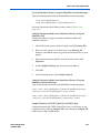
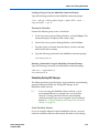
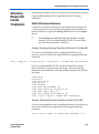
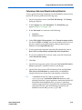
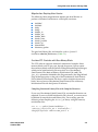
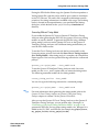
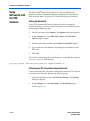
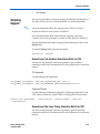
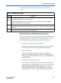
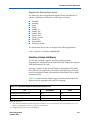
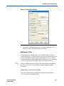
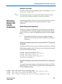
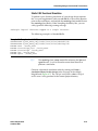
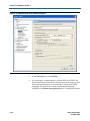
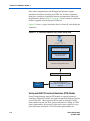
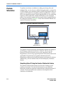
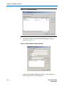
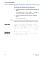
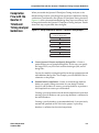
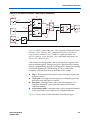
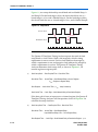
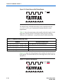
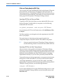
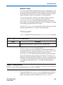
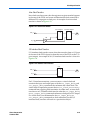
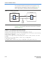
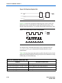
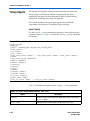
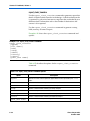
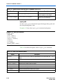
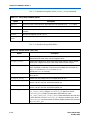
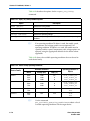
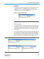
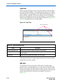
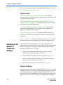
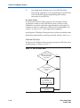
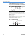
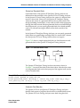
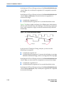
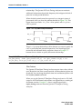
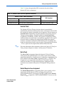
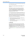
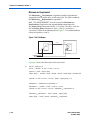
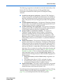
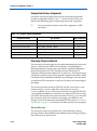
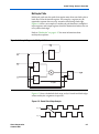
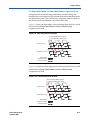
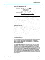
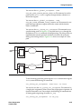
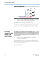
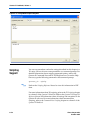
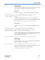
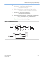
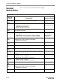
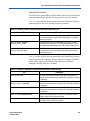
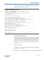
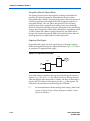
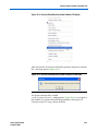
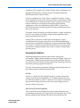
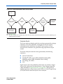
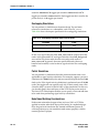
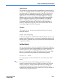
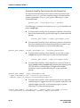
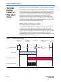
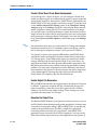
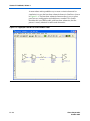
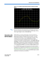
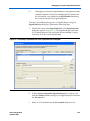
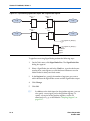
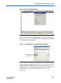
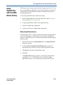
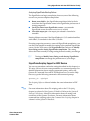
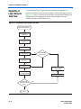
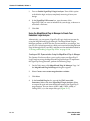
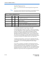
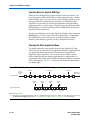
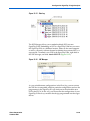
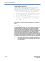
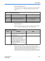
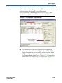
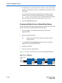
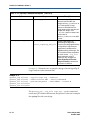
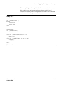
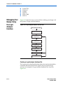
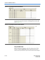
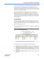
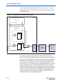
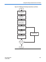
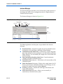
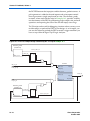
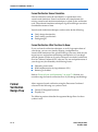
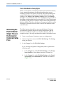
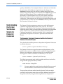
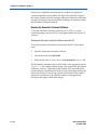
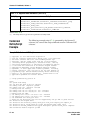
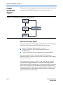
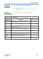
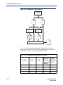
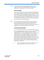
Timing Analysis Overview
The launch edge is an active clock edge that sends data out of a sequential
element, acting as a source for the data transfer. A latch edge is the active
clock edge that captures data at the data port of a sequential element,
acting as a destination for the data transfer.
Figure 6–7 shows a single-cycle system that uses consecutive clock edges
to transfer and capture data, a register-to-register path, and the
corresponding launch and latch edges timing diagram. In this example,
the launch edge sends the data out of register reg1 at 0 ns, and register
reg2 latch edge captures the data at 5 ns.
Figure 6–7. Launch Edge and Latch Edge
D
Q
D
reg1
Q
reg2
clk
Launch Edge at Source Register reg1
Latch Edge at Destination Register reg2
clk
0 ns
5 ns
10 ns
15 ns
The Quartus II TimeQuest Timing Analyzer validates clock setup and
hold requirements relative to the launch and latch edges.
Clock Analysis
A comprehensive static timing analysis includes analysis of
register-to-register, I/O, and asynchronous reset paths. The Quartus II
TimeQuest Timing Analyzer uses data required times, data arrival times,
and clock arrival times to verify circuit performance and detect possible
timing violations. The Quartus II TimeQuest Timing Analyzer
determines the timing relationships that must be met for the design to
correctly function, and checks arrival times against required times to
verify timing.
Clock Setup Check
To perform a clock setup check, the Quartus II TimeQuest Timing
Analyzer determines a setup relationship by analyzing each launch and
latch edge for each register-to-register path. For each latch edge at the
destination register, the Quartus II TimeQuest Timing Analyzer uses the
closest previous clock edge at the source register as the launch edge. In
Altera Corporation
October 2007
6–11
Preliminary