1
14. In-System Debugging
Using External Logic
Analyzers
QII53016-7.2.0
Introduction
The phenomenal growth in design size and complexity continues to make
the process of design verification a critical bottleneck for today’s FPGA
systems. Limited access to internal signals, advanced FPGA packages,
and printed circuit board (PCB) electrical noise are all contributing factors
in making design debugging and verification the most difficult process of
the design cycle. You can easily spend more than 50% of your design
cycle time debugging and verifying your design. To help you with the
process of design debugging and verification, Altera® provides a solution
that allows you to examine the behavior of internal signals using an
external logic analyzer and using a minimal number of FPGA I/O pins,
while your design is running at full speed on your FPGA.
1
This chapter's use of ‘logic analyzer’ includes both logic
analyzers and oscilloscopes equipped with digital channels,
commonly referred to as mixed signal analyzers or MSOs.
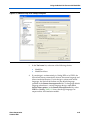
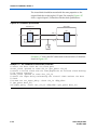
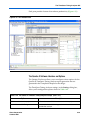
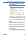
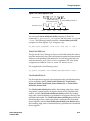
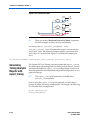
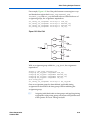
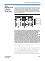
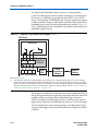
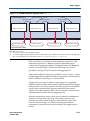
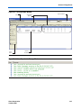
The Logic Analyzer Interface is an application within the Quartus II
software used to connect a large set of internal device signals to a small
number of output pins. You can connect these output pins to an external
logic analyzer for debugging purposes. The Logic Analyzer Interface
enables you to connect to and transmit internal signals buried within
your FPGA to an external logic analyzer for analysis. The Quartus II
Logic Analyzer Interface allows you to debug a large set of internal
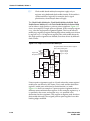
signals using a small number of output pins. In the Quartus II Logic
Analyzer Interface, the internal signals are grouped together, distributed
to a user-configurable multiplexer, and then output to available I/O pins
on your FPGA. Instead of having a one-to-one relationship between
internal signals to output pins, the Quartus II Logic Analyzer Interface
enables you map many internal signals to a smaller number of output
pins. The exact number of internal signals that you can map to an output
pin varies based on the multiplexer settings in the Quartus II Logic
Analyzer Interface.
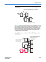
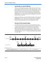
Optionally, you can use the Logic Analyzer Interface with the Quartus II
Incremental Compilation.
Altera Corporation
October 2007
14–1
Preliminary