1
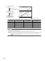
MELSEC-L Analog-Digital Converter Module
User's Manual
-L60AD4
-L60ADVL8
-L60ADIL8
SAFETY PRECAUTIONS
(Read these precautions before using this product.)
Before using this product, please read this manual and the relevant manuals carefully and pay full attention
to safety to handle the product correctly.
The precautions given in this manual are concerned with this product only. For the safety precautions of the
programmable controller system, refer to the user’s manual for the CPU module used.
In this manual, the safety precautions are classified into two levels: "
WARNING" and "
CAUTION".
WARNING
Indicates that incorrect handling may cause hazardous conditions,
resulting in death or severe injury.
CAUTION
Indicates that incorrect handling may cause hazardous conditions,
resulting in minor or moderate injury or property damage.
Under some circumstances, failure to observe the precautions given under “CAUTION” may lead to serious
consequences.
Observe the precautions of both levels because they are important for personal and system safety.
Make sure that the end users read this manual and then keep the manual in a safe place for future
reference.
[Design Precautions]
WARNING
● Do not write any data to the "system area" and "write-protect area" (R) of the buffer memory in the
intelligent function module. Also, do not use any “use prohibited” signals as an output signal from the
programmable controller CPU to the intelligent function module.
Doing so may cause malfunction of the programmable controller system.
[Design Precautions]
CAUTION
● Do not install the control lines or communication cables together with the main circuit lines or power
cables. Keep a distance of 100mm or more between them. Failure to do so may result in malfunction
due to noise.
[Installation Precautions]
WARNING
● Shut off the external power supply (all phases) used in the system before mounting or removing a
module. Failure to do so may result in electric shock or cause the module to fail or malfunction.
1
[Installation Precautions]
CAUTION
● Use the programmable controller in an environment that meets the general specifications in the Safety
Guidelines provided with the CPU module or head module. Failure to do so may result in electric
shock, fire, malfunction, or damage to or deterioration of the product.
● To interconnect modules, engage the respective connectors and securely lock the module joint levers
until they click. Incorrect interconnection may cause malfunction, failure, or drop of the module.
● Tighten the screws within the specified torque range. Undertightening can cause drop of the screw,
short circuit, or malfunction. Overtightening can damage the screw and/or module, resulting in drop,
short circuit, or malfunction.
● Do not directly touch any conductive parts and electronic components of the module. Doing so can
cause malfunction or failure of the module.
[Wiring Precautions]
WARNING
● After installation and wiring, attach the included terminal cover to the module before turning it on for
operation. Failure to do so may result in electric shock.
[Wiring Precautions]
CAUTION
● Individually ground the FG terminal of the programmable controller with a ground resistance of 100
ohms or less. Failure to do so may result in electric shock or malfunction.
● Tighten the terminal block screws within the specified torque range. Undertightening can cause short
circuit, fire, or malfunction. Overtightening can damage the screw and/or module, resulting in drop,
short circuit, or malfunction.
● Prevent foreign matter such as dust or wire chips from entering the module. Such foreign matter can
cause a fire, failure, or malfunction.
● A protective film is attached to the top of the module to prevent foreign matter, such as wire chips,
from entering the module during wiring. Do not remove the film during wiring. Remove it for heat
dissipation before system operation.
● Mitsubishi programmable controllers must be installed in control panels. Connect the main power
supply to the power supply module in the control panel through a relay terminal block. Wiring and
replacement of a power supply module must be performed by qualified maintenance personnel with
knowledge of protection against electric shock. For wiring methods, refer to the MELSEC-L CPU
Module User's Manual (Hardware Design, Maintenance and Inspection).
2
[Startup and Maintenance Precautions]
WARNING
● Do not touch any terminal while power is on. Doing so will cause electric shock or malfunction.
● Shut off the external power supply (all phases) used in the system before cleaning the module or
retightening the terminal block screws. Failure to do so may result in electric shock.
[Startup and Maintenance Precautions]
CAUTION
● Do not disassemble or modify the module. Doing so may cause failure, malfunction, injury, or a fire.
● Shut off the external power supply (all phases) used in the system before mounting or removing a
module. Failure to do so may cause the module to fail or malfunction.
● Tighten the terminal block screws within the specified torque range. Undertightening can cause drop
of the component or wire, short circuit, or malfunction. Overtightening can damage the screw and/or
module, resulting in drop, short circuit, or malfunction.
● After the first use of the product (module, display unit, and terminal block), do not connect/disconnect
the product more than 50 times (in accordance with IEC 61131-2). Exceeding the limit may cause
malfunction.
● Before handling the module, touch a conducting object such as a grounded metal to discharge the
static electricity from the human body. Failure to do so may cause the module to fail or malfunction.
[Disposal Precautions]
CAUTION
● When disposing of this product, treat it as industrial waste.
3
CONDITIONS OF USE FOR THE PRODUCT
(1) Mitsubishi programmable controller ("the PRODUCT") shall be used in conditions;
i) where any problem, fault or failure occurring in the PRODUCT, if any, shall not lead to any major or serious accident;
and
ii) where the backup and fail-safe function are systematically or automatically provided outside of the PRODUCT for the
case of any problem, fault or failure occurring in the PRODUCT.
(2) The PRODUCT has been designed and manufactured for the purpose of being used in general industries.
MITSUBISHI SHALL HAVE NO RESPONSIBILITY OR LIABILITY (INCLUDING, BUT NOT LIMITED TO ANY AND ALL
RESPONSIBILITY OR LIABILITY BASED ON CONTRACT, WARRANTY, TORT, PRODUCT LIABILITY) FOR ANY
INJURY OR DEATH TO PERSONS OR LOSS OR DAMAGE TO PROPERTY CAUSED BY the PRODUCT THAT ARE
OPERATED OR USED IN APPLICATION NOT INTENDED OR EXCLUDED BY INSTRUCTIONS, PRECAUTIONS, OR
WARNING CONTAINED IN MITSUBISHI'S USER, INSTRUCTION AND/OR SAFETY MANUALS, TECHNICAL
BULLETINS AND GUIDELINES FOR the PRODUCT.
("Prohibited Application")
Prohibited Applications include, but not limited to, the use of the PRODUCT in;
• Nuclear Power Plants and any other power plants operated by Power companies, and/or any other cases in which the
public could be affected if any problem or fault occurs in the PRODUCT.
• Railway companies or Public service purposes, and/or any other cases in which establishment of a special quality
assurance system is required by the Purchaser or End User.
• Aircraft or Aerospace, Medical applications, Train equipment, transport equipment such as Elevator and Escalator,
Incineration and Fuel devices, Vehicles, Manned transportation, Equipment for Recreation and Amusement, and
Safety devices, handling of Nuclear or Hazardous Materials or Chemicals, Mining and Drilling, and/or other
applications where there is a significant risk of injury to the public or property.
Notwithstanding the above, restrictions Mitsubishi may in its sole discretion, authorize use of the PRODUCT in one or
more of the Prohibited Applications, provided that the usage of the PRODUCT is limited only for the specific
applications agreed to by Mitsubishi and provided further that no special quality assurance or fail-safe, redundant or
other safety features which exceed the general specifications of the PRODUCTs are required. For details, please
contact the Mitsubishi representative in your region.
4
INTRODUCTION
Thank you for purchasing the Mitsubishi MELSEC-L series programmable controllers.
This manual describes the functions and programming of an analog-digital converter module (hereafter abbreviated as
A/D converter module).
Before using this product, please read this manual and the relevant manuals carefully and develop familiarity with the
functions and performance of the MELSEC-L series programmable controller to handle the product correctly.
When applying the program examples introduced in this manual to an actual system, ensure the applicability and
confirm that it will not cause system control problems.
Relevant modules: L60AD4, L60ADVL8, L60ADIL8
Remark
● Unless otherwise specified, this manual describes the program examples in which the I/O numbers of X/Y00 to X/Y0F are
assigned for an A/D converter module.
For I/O number assignment, refer to the following.
MELSEC-L CPU Module User's Manual (Function Explanation, Program Fundamentals)
● Operating procedures are explained using GX Works2. When using GX Developer or GX Configurator-AD, refer to the
following.
• When using GX Developer or GX Configurator-AD (
Page 263, Appendix 9)
5
COMPLIANCE WITH EMC AND LOW VOLTAGE
DIRECTIVES
(1) Method of ensuring compliance
To ensure that Mitsubishi programmable controllers maintain EMC and Low Voltage Directives when incorporated
into other machinery or equipment, certain measures may be necessary. Please refer to one of the following
manuals.
• MELSEC-L CPU Module User's Manual (Hardware Design, Maintenance and Inspection)
• MELSEC-L CC-Link IE Field Network Head Module User's Manual
• Safety Guidelines (This manual is included with the CPU module or base unit.)
The CE mark on the side of the programmable controller indicates compliance with EMC and Low Voltage
Directives.
(2) Additional measures
No additional measures are necessary for the compliance of this product with the EMC and Low Voltage
Directives.
6
RELEVANT MANUALS
(1) CPU module user’s manual
Manual name
manual number (model code)
Description
MELSEC-L CPU Module User's Manual (Hardware Design, Maintenance and
Inspection)
SH-080890ENG, 13JZ36
Specifications of the CPU modules, power supply modules, display unit,
branch module, extension module, SD memory cards, and batteries,
information on how to establish a system, maintenance and inspection, and
troubleshooting
MELSEC-L CPU Module User's Manual (Function Explanation, Program
Fundamentals)
SH-080889ENG, 13JZ35
Functions and devices of the CPU module, and programming
(2) Head module User’s Manual
Manual name
manual number (model code)
Description
MELSEC-L CC-Link IE Field Network Head Module User's Manual
SH-080919ENG, 13JZ48
Specifications, procedures before operation, system configuration, installation,
wiring, settings, and troubleshooting of the head module
(3) Operating manual
Manual name
manual number (model code)
Description
GX Works2 Version 1 Operating Manual (Common)
SH-080779ENG, 13JU63
GX Developer Version 8 Operating Manual
SH-080373E, 13JU41
System configuration, parameter settings, and online operations of GX
Works2, which are common to Simple projects and Structured projects
Operating methods of GX Developer, such as programming, printing,
monitoring, and debugging
7
CONTENTS
CONTENTS
SAFETY PRECAUTIONS . . . . . . . . . . . . . . . . . . . . . . . . . . . . . . . . . . . . . . . . . . . . . . . . . . . . . . . . . . . . . 1
CONDITIONS OF USE FOR THE PRODUCT . . . . . . . . . . . . . . . . . . . . . . . . . . . . . . . . . . . . . . . . . . . . . 4
INTRODUCTION . . . . . . . . . . . . . . . . . . . . . . . . . . . . . . . . . . . . . . . . . . . . . . . . . . . . . . . . . . . . . . . . . . . . 5
COMPLIANCE WITH EMC AND LOW VOLTAGE DIRECTIVES . . . . . . . . . . . . . . . . . . . . . . . . . . . . . . . 6
RELEVANT MANUALS . . . . . . . . . . . . . . . . . . . . . . . . . . . . . . . . . . . . . . . . . . . . . . . . . . . . . . . . . . . . . . . 7
MANUAL PAGE ORGANIZATION . . . . . . . . . . . . . . . . . . . . . . . . . . . . . . . . . . . . . . . . . . . . . . . . . . . . . . 11
TERMS . . . . . . . . . . . . . . . . . . . . . . . . . . . . . . . . . . . . . . . . . . . . . . . . . . . . . . . . . . . . . . . . . . . . . . . . . . 15
PACKING LIST . . . . . . . . . . . . . . . . . . . . . . . . . . . . . . . . . . . . . . . . . . . . . . . . . . . . . . . . . . . . . . . . . . . . 15
CHAPTER 1 A/D CONVERTER MODULE
1.1
Application . . . . . . . . . . . . . . . . . . . . . . . . . . . . . . . . . . . . . . . . . . . . . . . . . . . . . . . . . . . . . . . . 16
1.2
Features . . . . . . . . . . . . . . . . . . . . . . . . . . . . . . . . . . . . . . . . . . . . . . . . . . . . . . . . . . . . . . . . . . 17
CHAPTER 2 PART NAMES
18
CHAPTER 3 SPECIFICATIONS
20
3.1
3.2
General Specifications . . . . . . . . . . . . . . . . . . . . . . . . . . . . . . . . . . . . . . . . . . . . . . . . . . . . . . . 20
Performance Specifications . . . . . . . . . . . . . . . . . . . . . . . . . . . . . . . . . . . . . . . . . . . . . . . . . . . 21
3.2.1
Number of parameter settings . . . . . . . . . . . . . . . . . . . . . . . . . . . . . . . . . . . . . . . . . . . . . . . . .24
3.3
Function List . . . . . . . . . . . . . . . . . . . . . . . . . . . . . . . . . . . . . . . . . . . . . . . . . . . . . . . . . . . . . . . 25
3.4
I/O Signal List . . . . . . . . . . . . . . . . . . . . . . . . . . . . . . . . . . . . . . . . . . . . . . . . . . . . . . . . . . . . . . 27
3.5
List of Buffer Memory Addresses . . . . . . . . . . . . . . . . . . . . . . . . . . . . . . . . . . . . . . . . . . . . . . . 28
CHAPTER 4 PROCEDURES BEFORE STARTING THE OPERATION
41
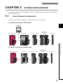
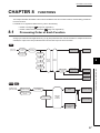
CHAPTER 5 SYSTEM CONFIGURATION
43
5.1
Overall System Configuration . . . . . . . . . . . . . . . . . . . . . . . . . . . . . . . . . . . . . . . . . . . . . . . . . . 43
5.2
Applicable System . . . . . . . . . . . . . . . . . . . . . . . . . . . . . . . . . . . . . . . . . . . . . . . . . . . . . . . . . . 44
5.3
Restrictions When A/D Converter Module is Connected to Head Module . . . . . . . . . . . . . . . . 44
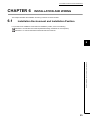
CHAPTER 6 INSTALLATION AND WIRING
45
6.1
Installation Environment and Installation Position . . . . . . . . . . . . . . . . . . . . . . . . . . . . . . . . . . 45
6.2
Terminal Block . . . . . . . . . . . . . . . . . . . . . . . . . . . . . . . . . . . . . . . . . . . . . . . . . . . . . . . . . . . . . 46
6.3
Wiring . . . . . . . . . . . . . . . . . . . . . . . . . . . . . . . . . . . . . . . . . . . . . . . . . . . . . . . . . . . . . . . . . . . . 49
6.4
External Wiring . . . . . . . . . . . . . . . . . . . . . . . . . . . . . . . . . . . . . . . . . . . . . . . . . . . . . . . . . . . . . 51
CHAPTER 7 VARIOUS SETTINGS
53
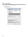
7.1
Addition of Modules . . . . . . . . . . . . . . . . . . . . . . . . . . . . . . . . . . . . . . . . . . . . . . . . . . . . . . . . . 53
7.2
Switch Setting . . . . . . . . . . . . . . . . . . . . . . . . . . . . . . . . . . . . . . . . . . . . . . . . . . . . . . . . . . . . . . 54
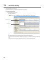
7.3
Parameter Setting. . . . . . . . . . . . . . . . . . . . . . . . . . . . . . . . . . . . . . . . . . . . . . . . . . . . . . . . . . . 56
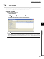
7.4
Auto Refresh. . . . . . . . . . . . . . . . . . . . . . . . . . . . . . . . . . . . . . . . . . . . . . . . . . . . . . . . . . . . . . . 59
7.5
Offset/Gain Setting . . . . . . . . . . . . . . . . . . . . . . . . . . . . . . . . . . . . . . . . . . . . . . . . . . . . . . . . . . 60
7.5.1
8
16
Setting from GX Works2 "Offset/Gain Setting". . . . . . . . . . . . . . . . . . . . . . . . . . . . . . . . . . . . .60
7.5.2
Setting from a program . . . . . . . . . . . . . . . . . . . . . . . . . . . . . . . . . . . . . . . . . . . . . . . . . . . . . .63
CHAPTER 8 FUNCTIONS
67
8.1
Processing Order of Each Function . . . . . . . . . . . . . . . . . . . . . . . . . . . . . . . . . . . . . . . . . . . . . 67
8.2
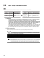
A/D Conversion Enable/Disable Function. . . . . . . . . . . . . . . . . . . . . . . . . . . . . . . . . . . . . . . . . 69
8.3
A/D Conversion Method . . . . . . . . . . . . . . . . . . . . . . . . . . . . . . . . . . . . . . . . . . . . . . . . . . . . . . 69
8.4
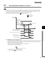
Input Range Extension Function. . . . . . . . . . . . . . . . . . . . . . . . . . . . . . . . . . . . . . . . . . . . . . . . 74
8.5
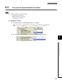
Conversion Speed Switch Function . . . . . . . . . . . . . . . . . . . . . . . . . . . . . . . . . . . . . . . . . . . . . 75
8.6
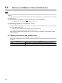
Maximum and Minimum Values Hold Function. . . . . . . . . . . . . . . . . . . . . . . . . . . . . . . . . . . . . 76
8.7
Input Signal Error Detection Function. . . . . . . . . . . . . . . . . . . . . . . . . . . . . . . . . . . . . . . . . . . . 77
8.8
Input Signal Error Detection Extension Function . . . . . . . . . . . . . . . . . . . . . . . . . . . . . . . . . . . 82
8.9
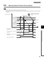
Warning Output Function (Process Alarm) . . . . . . . . . . . . . . . . . . . . . . . . . . . . . . . . . . . . . . . . 85
8.10
Scaling Function . . . . . . . . . . . . . . . . . . . . . . . . . . . . . . . . . . . . . . . . . . . . . . . . . . . . . . . . . . . . 88
8.11
Shift Function . . . . . . . . . . . . . . . . . . . . . . . . . . . . . . . . . . . . . . . . . . . . . . . . . . . . . . . . . . . . . . 94
8.12
Digital Clipping Function . . . . . . . . . . . . . . . . . . . . . . . . . . . . . . . . . . . . . . . . . . . . . . . . . . . . . . 99
8.13
Difference Conversion Function . . . . . . . . . . . . . . . . . . . . . . . . . . . . . . . . . . . . . . . . . . . . . . . 103
8.14
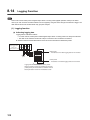
Logging Function . . . . . . . . . . . . . . . . . . . . . . . . . . . . . . . . . . . . . . . . . . . . . . . . . . . . . . . . . . 108
8.14.1 Stopping logging. . . . . . . . . . . . . . . . . . . . . . . . . . . . . . . . . . . . . . . . . . . . . . . . . . . . . . . . . . . 115
8.14.2 Logging hold request . . . . . . . . . . . . . . . . . . . . . . . . . . . . . . . . . . . . . . . . . . . . . . . . . . . . . . . 118
8.14.3 Level trigger . . . . . . . . . . . . . . . . . . . . . . . . . . . . . . . . . . . . . . . . . . . . . . . . . . . . . . . . . . . . . . 119
8.14.4 Initial setting for the logging function . . . . . . . . . . . . . . . . . . . . . . . . . . . . . . . . . . . . . . . . . . .122
8.15
Flow Amount Integration Function . . . . . . . . . . . . . . . . . . . . . . . . . . . . . . . . . . . . . . . . . . . . . 123
8.16
Error Log Function . . . . . . . . . . . . . . . . . . . . . . . . . . . . . . . . . . . . . . . . . . . . . . . . . . . . . . . . . 133
8.17
Module Error Collection Function . . . . . . . . . . . . . . . . . . . . . . . . . . . . . . . . . . . . . . . . . . . . . . 136
8.18
Error Clear Function . . . . . . . . . . . . . . . . . . . . . . . . . . . . . . . . . . . . . . . . . . . . . . . . . . . . . . . . 137
8.19
Saving and Restoring Offset/Gain Values . . . . . . . . . . . . . . . . . . . . . . . . . . . . . . . . . . . . . . . 138
CHAPTER 9 DISPLAY UNIT
145
9.1
Display Unit. . . . . . . . . . . . . . . . . . . . . . . . . . . . . . . . . . . . . . . . . . . . . . . . . . . . . . . . . . . . . . . 145
9.2
Menu Transition . . . . . . . . . . . . . . . . . . . . . . . . . . . . . . . . . . . . . . . . . . . . . . . . . . . . . . . . . . . 145
9.3
List of Setting Value Change Screens . . . . . . . . . . . . . . . . . . . . . . . . . . . . . . . . . . . . . . . . . . 149
9.4
Checking and Clearing Errors. . . . . . . . . . . . . . . . . . . . . . . . . . . . . . . . . . . . . . . . . . . . . . . . . 155
CHAPTER 10 PROGRAMMING
157
10.1
Procedure for Programming . . . . . . . . . . . . . . . . . . . . . . . . . . . . . . . . . . . . . . . . . . . . . . . . . . 157
10.2
When Using the Module in a Standard System Configuration . . . . . . . . . . . . . . . . . . . . . . . . 158
10.3
When A/D Converter Module is Connected to Head Module . . . . . . . . . . . . . . . . . . . . . . . . . 166
CHAPTER 11 TROUBLESHOOTING
175
11.1
Checking on the Module Detailed Information . . . . . . . . . . . . . . . . . . . . . . . . . . . . . . . . . . . . 176
11.2
Checking by Latest Error Code (Un\G19). . . . . . . . . . . . . . . . . . . . . . . . . . . . . . . . . . . . . . . . 177
11.3
Checking on the Module Error Collection Function . . . . . . . . . . . . . . . . . . . . . . . . . . . . . . . . 178
11.4
Error Code List . . . . . . . . . . . . . . . . . . . . . . . . . . . . . . . . . . . . . . . . . . . . . . . . . . . . . . . . . . . . 179
9
11.5
Alarm Code List . . . . . . . . . . . . . . . . . . . . . . . . . . . . . . . . . . . . . . . . . . . . . . . . . . . . . . . . . . . 183
11.6
Troubleshooting . . . . . . . . . . . . . . . . . . . . . . . . . . . . . . . . . . . . . . . . . . . . . . . . . . . . . . . . . . . 184
11.7
11.6.1
Troubleshooting using LEDs . . . . . . . . . . . . . . . . . . . . . . . . . . . . . . . . . . . . . . . . . . . . . . . . .184
11.6.2
Troubleshooting for the A/D conversion . . . . . . . . . . . . . . . . . . . . . . . . . . . . . . . . . . . . . . . . .186
Checking the Status of the A/D Converter Module by the System Monitor . . . . . . . . . . . . . . 191
APPENDICES
192
Appendix 1 Details of I/O Signals. . . . . . . . . . . . . . . . . . . . . . . . . . . . . . . . . . . . . . . . . . . . . . . . . . . 192
Appendix 1.1
Input signal. . . . . . . . . . . . . . . . . . . . . . . . . . . . . . . . . . . . . . . . . . . . . . . . . . . . . . . . .192
Appendix 1.2
Output signal . . . . . . . . . . . . . . . . . . . . . . . . . . . . . . . . . . . . . . . . . . . . . . . . . . . . . . .197
Appendix 2 Details of Buffer Memory Addresses . . . . . . . . . . . . . . . . . . . . . . . . . . . . . . . . . . . . . . 199
Appendix 3 I/O Conversion Characteristic of A/D Conversion . . . . . . . . . . . . . . . . . . . . . . . . . . . . . 235
Appendix 4 A/D Conversion Accuracy . . . . . . . . . . . . . . . . . . . . . . . . . . . . . . . . . . . . . . . . . . . . . . . 240
Appendix 5 Dedicated Instructions. . . . . . . . . . . . . . . . . . . . . . . . . . . . . . . . . . . . . . . . . . . . . . . . . . 241
Appendix 5.1
Instruction list . . . . . . . . . . . . . . . . . . . . . . . . . . . . . . . . . . . . . . . . . . . . . . . . . . . . . . .241
Appendix 5.2
G(P).OFFGAN . . . . . . . . . . . . . . . . . . . . . . . . . . . . . . . . . . . . . . . . . . . . . . . . . . . . . .242
Appendix 5.3
G(P).OGLOAD . . . . . . . . . . . . . . . . . . . . . . . . . . . . . . . . . . . . . . . . . . . . . . . . . . . . . .244
Appendix 5.4
G(P).OGSTOR . . . . . . . . . . . . . . . . . . . . . . . . . . . . . . . . . . . . . . . . . . . . . . . . . . . . . .249
Appendix 6 Checking Serial Number and Function Version . . . . . . . . . . . . . . . . . . . . . . . . . . . . . . 254
Appendix 7 Addition and Change of Functions . . . . . . . . . . . . . . . . . . . . . . . . . . . . . . . . . . . . . . . . 256
Appendix 7.1
Addition of functions. . . . . . . . . . . . . . . . . . . . . . . . . . . . . . . . . . . . . . . . . . . . . . . . . .256
Appendix 7.2
Change of functions . . . . . . . . . . . . . . . . . . . . . . . . . . . . . . . . . . . . . . . . . . . . . . . . . .256
Appendix 8 Differences with Q Series . . . . . . . . . . . . . . . . . . . . . . . . . . . . . . . . . . . . . . . . . . . . . . . 259
Appendix 8.1
Precautions for Applying Q Series Sequence Program . . . . . . . . . . . . . . . . . . . . . . .260
Appendix 9 When Using GX Developer or GX Configurator-AD . . . . . . . . . . . . . . . . . . . . . . . . . . . 263
Appendix 9.1
Operation of GX Developer . . . . . . . . . . . . . . . . . . . . . . . . . . . . . . . . . . . . . . . . . . . .263
Appendix 9.2
Operation of GX Configurator-AD . . . . . . . . . . . . . . . . . . . . . . . . . . . . . . . . . . . . . . .265
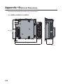
Appendix 10 External Dimensions . . . . . . . . . . . . . . . . . . . . . . . . . . . . . . . . . . . . . . . . . . . . . . . . . . . 268
INDEX
269
INSTRUCTION INDEX
271
REVISIONS . . . . . . . . . . . . . . . . . . . . . . . . . . . . . . . . . . . . . . . . . . . . . . . . . . . . . . . . . . . . . . . . . . . . . . 272
WARRANTY . . . . . . . . . . . . . . . . . . . . . . . . . . . . . . . . . . . . . . . . . . . . . . . . . . . . . . . . . . . . . . . . . . . . . 273
TRADEMARKS . . . . . . . . . . . . . . . . . . . . . . . . . . . . . . . . . . . . . . . . . . . . . . . . . . . . . . . . . . . . . . . . . . . 274
10
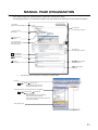
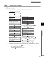
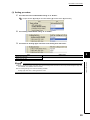
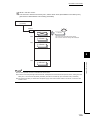
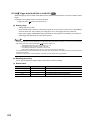
MANUAL PAGE ORGANIZATION
In this manual, pages are organized and the symbols are used as shown below.
The following illustration is for explanation purpose only, and should not be referred to as an actual documentation.
"" is used for
screen names and items.
The chapter of
the current page is shown.
shows operating
procedures.
shows mouse
operations.*1
[ ] is used for items
in the menu bar and
the project window.
The section of
the current page is shown.
Ex. shows setting or
operating examples.
shows reference
manuals.
shows notes that
requires attention.
shows
reference pages.
shows useful
information.
*1
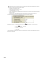
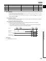
The mouse operation example (for GX Works2) is provided below.
Menu bar
Ex.
[Online]
[Write to PLC...]
Select [Online] on the menu bar,
and then select [Write to PLC...].
A window selected in the view selection area is displayed.
Ex.
[Parameter]
Project window
[PLC Parameter]
Select [Project] from the view selection
area to open the Project window.
In the Project window, expand [Parameter] and
select [PLC Parameter].
View selection area
11
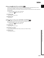
Pages describing instructions are organized as shown below.
The following illustration is for explanation purpose only, and should not be referred to as an actual documentation.
Instruction name
Execution condition of the instruction
Structure of the instruction
in the ladder mode
shows the devices
applicable to the instruction
Descriptions of
setting data and data type
Descriptions of
control data (if any)
12
Setting side
User : Device value is set by the user.
System: Device value is set by
the CPU module.
Detailed descriptions
of the instruction
Conditions for the error and
error codes
For the errors not described in
this manual, refer to the following.
MELSEC-L CPU Module
User's Manual (Hardware Design,
Maintenance and Inspection)
Simple program example(s)
and descriptions of the devices used
• Instructions can be executed under the following conditions.
Execution condition
Symbol
Any time
During on
On the rising edge
During off
On the falling edge
No symbol
• The following devices can be used.
Setting
data
Internal device (system,
user)
Bit
Applicable
device *2
X, Y, M, L,
SM, F, B,
SB, FX, FY
*3
File
register
Word
T, ST, C, D,
W, SD, SW,
FD, @
Link direct
device
J\
Bit
R, ZR
Word
Intelligent function
module
U\G
Index
register
Zn
Constant*4
Others*4
U\G
Z
K, H, E, $
P, I, J, U, D, X,
DY, N, BL, TR,
BL\S, V
-
*2
For details on each device, refer to the following.
*3
*4
MELSEC-L CPU Module User's Manual (Function Explanation, Program Fundamentals)
FX and FY can be used for bit data only, and FD for word data only.
In the “Constant” and “Others” columns, a device(s) that can be set for each instruction is shown.
• The following data types can be used.
Data type
Description
Bit
Bit data or the start number of bit data
BIN 16-bit
16-bit binary data or the start number of word device
BIN 32-bit
32-bit binary data or the start number of double-word device
BCD 4-digit
Four-digit binary-coded decimal data
BCD 8-digit
Eight-digit binary-coded decimal data
Real number
Floating-point data
Character string
Character string data
Device name
Device name data
13
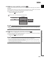
Pages describing functions, I/O signals, and buffer memory areas are organized as shown below.
The following illustration is for explanation purpose only, and should not be referred to as an actual documentation.
Each icon indicates the available module.
The meaning of each icon is as follows.
Icon
Common
AD4
14
Description
The corresponding buffer memory area, I/O signal, or function is common to the A/D converter modules regardless of the model.
The corresponding buffer memory area, I/O signal, or function is for the L60AD4.
ADVL8
The corresponding buffer memory area, I/O signal, or function is for the L60ADVL8.
ADIL8
The corresponding buffer memory area, I/O signal, or function is for the L60ADIL8.
TERMS
Unless otherwise specified, this manual uses the following terms.
Term
Description
A/D converter module
A generic term for the L60AD4, L60ADVL8, and L60ADIL8
Buffer memory
A memory in an intelligent function module, where data (such as setting values and monitoring values) exchanged with a
CPU module are stored
Display unit
A liquid crystal display to be attached to the CPU module
Factory default setting
A generic term for analog input ranges of 0 to 10V, 0 to 5V, 1 to 5V, -10 to 10V, 0 to 20mA, and 4 to 20mA
GX Configurator-AD
A setting and monitoring tool added in GX Developer (for A/D converter modules)
GX Developer
GX Works2
The product name of the software package for the MELSEC programmable controllers
Head module
The abbreviation for the LJ72GF15-T2 CC-Link IE Field Network head module
L60AD4
The abbreviation for the L60AD4 analog-digital converter module
L60ADIL8
The abbreviation for the L60ADIL8 analog-digital converter module
L60ADVL8
The abbreviation for the L60ADVL8 analog-digital converter module
Normal mode
The drive modes set in the switch setting window. Note that the normal mode is displayed as "Normal (A/D Converter
Processing, D/A Converter Processing) Mode" on the programming tool.
Offset/gain setting mode
Programming tool
A generic term for GX Works2 and GX Developer
Switch setting
A generic term for the setting items in the window that is displayed by double-clicking "Switch Setting" of the specified
module on the project window of GX Works2
User range setting
An analog input range where a user can set any values. To use this range, the offset and gain values have to be set.
Watchdog timer error
An error that occurs if the internal processing of the A/D converter module fails. The module monitors its own internal
processing by using the watchdog timer.
PACKING LIST
The following items are included in the package of this product. Before use, check that all the items are included.
A/D converter module
A/D converter module
Before Using the Product
15
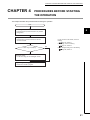
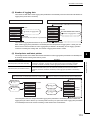
CHAPTER 1
A/D CONVERTER MODULE
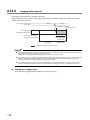
This chapter describes the applications and features of the A/D converter module.
1.1
Application
This module converts the analog value input from external devices to the digital output value, and inputs the converted
data to the CPU module. By converting the data, which has been processed through the A/D converter module, to a
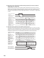
digital data, the input information can be sent to the CPU module.
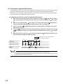
Analog to digital
conversion
Analog signal (continuous signal)
Digital signal (discrete signal)
The A/D converter module enables works as follows.
Connect the module to the control valve to measure the flow
Control valve
Flow control
Connect the module to the power conditioning equipment to measure the
heating temperature of the heater or others
Power conditioner
Tank
Heater
16
CHAPTER 1 A/D CONVERTER MODULE
1.2
Features
1
(1) Common features of the A/D converter module
(a) Comparing/monitoring the measurement target
By using the input signal error detection function, input range extension function, or alarm output function
(process alarm), the statuses of connected devices can be monitored easily.
(b) Easy setting with GX Works2
Programming is reduced since the initial setting or auto refresh setting can be configured on the screen. In
addition, setting status and operation status of modules can be checked easily.
(2) Features of the L60AD4
(a) Response by high-speed conversion
The high-speed conversion of 20µs/channel is achieved.
(b) Detailed control by high resolution
In all analog input ranges, the high resolution of 1/20000 is achieved.
(c) Reliability by high accuracy
The accuracy for the maximum value of the digital output value is ±0.1% (25±5°C), ±0.2% (0 to 55°C).
(d) Operation of digital output values
The shift function, digital clipping function, and difference conversion function, as well as the scaling function,
can represent the digital output value in a numeric value easy to understand according to the use environment.
1.2 Features
(e) Logging function
An analysis of data collected by logging function increases maintainability of used system.
(f) Flow amount integration function
The flow amount integration function executes the integral processing of input (instantaneous flow amount)
from a flow meter and easily calculates the flow amount in a certain period. By registering/outputting the
calculated flow amount, system operation can be improved and man-hours for programming can be reduced.
(3) Features of the L60ADVL8 and L60ADIL8
The L60ADVL8 and L60ADIL8 have the same basic function as that of the L60AD4, and have the analog input
capability twice as that of the L60AD4 (eight channels). This reduces the number of analog input modules used,
lowers the cost, and saves the spaces in the system that uses a large number of analog inputs.
17
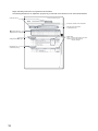
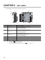
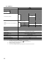
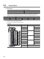
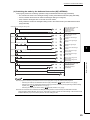
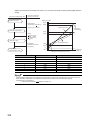
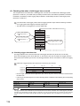
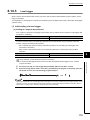
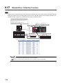
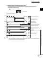
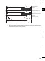
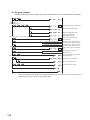
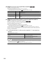
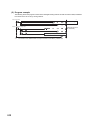
CHAPTER 2
PART NAMES
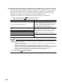
The following table shows part names of the A/D converter module.
1)
1)
2)
4)
3)
7)
6)
5)
1)
8)
1)
Number
1)
2)
Name
Description
Module joint levers
Levers for connecting modules
RUN LED (green)
Displays the operating status of the A/D converter module.
On: The module is operating normally.
Flashing: In the offset/gain setting mode
Off: The 5V power off or watchdog timer error has occurred.
Displays the errors and status of the A/D converter module.
3)
ERR. LED (red)
On: an error has occurred except for error code: 112*1
Flashing: Error code: 112 has occurred.*1
Off: The module is operating normally.
Displays the alarm status of the A/D converter module.
4)
ALM LED (red)
5)
DIN rail hook
Flashing: Input signal error detection is occurring*2
Off: The module is operating normally.
A hook used to mount the module to a DIN rail
6)
Terminal
7)
Terminal block cover
Covers for preventing electric shock while the power is on
8)
Serial number display
Displays the serial number printed on the rating plate.
*1
18
block*3
On: Alarm (process alarm) is occurring*2
Error Code List (
18-pin screw terminal block for connecting input signal lines of such as external devices
Page 179, Section 11.4)
*2
Alarm Code List (
*3
Terminal Block for the signal assignment of the terminal block
Page 183, Section 11.5)
Page 46, Section 6.2)
CHAPTER 2 PART NAMES
Memo
2
19
CHAPTER 3
SPECIFICATIONS
This chapter describes general specifications, performance specifications, function list, list of I/O signals and list of
buffer memory address.
3.1
General Specifications
For the general specifications of the A/D converter module, refer to the following.
The manual "Safety Guidelines", the manual supplied with the a CPU module or head module
20
CHAPTER 3 SPECIFICATIONS
3.2
Performance Specifications
The following table shows the performance specifications of the A/D converter module.
(1) L60AD4
Model
Item
Number of analog input channels
Analog input
Digital output
4 channels
Voltage
-10 to 10 VDC (input resistance 1M )
Current
0 to 20mADC (input resistance 250 )
Digital output value
-20480 to 20479
When using the scaling function
-32768 to 32767
Analog input range
Digital output value
0 to 10V
Voltage
I/O characteristics, resolution*1
0 to 20000
1 to 5V
-20000 to 20000
1 to 5V (Extended mode)
-5000 to 22500
200µV
User range setting
-20000 to 20000
307µV*2
0 to 20000
4 to 20mA
1000nA
800nA
4 to 20mA (Extended mode)
-5000 to 22500
800nA
User range setting
-20000 to 20000
1230nA*2
Ambient temperature
25±5°C
Within ±0.1% (±20digit)
Ambient temperature
0 to 55°C
Within ±0.2% (±40digit)
Conversion speed*4*5*6
500µV
High-speed: 20µs/channel
Medium speed: 80µs/channel
Low speed: 1ms/channel
Absolute maximum input
Voltage: ±15V, Current: 30mA*7
Offset/gain setting count*8
Up to 50000 counts
Between I/O terminals and programmable controller power supply: photocoupler isolation
Between input channels: no isolation
Isolation method
Dielectric withstand voltage
Between I/O terminals and programmable controller power supply: 500VACrms for 1 minute
Insulation resistance
Between I/O terminals and programmable controller power supply: 500VDC 10M or higher
Number of occupied I/O points
External interface
16 points (I/O assignment: Intelligent 16 points)
18-point terminal block
0.3 to 0.75mm2
Applicable wire size
Applicable solderless terminal
R1.25-3 (solderless terminals with sleeve are not usable)
Internal current consumption (5VDC)
0.52A
Weight
0.19kg
*1
*2
*3
*4
*5
*6
*7
*8
For details on the I/O conversion characteristics, refer to the following.
I/O conversion characteristic of A/D conversion (
Page 235, Appendix 3)
Maximum resolution in the user range setting.
Except when receiving noise influence.
The default value is 80µs/channel.
The logging function can be used only in the middle speed (80µs/channel) or low speed (1ms/channel).
The flow amount integration function can be used only in the low speed (1ms/channel).
This is a momentary current value which does not cause damage to internal resistors of the module. The maximum input
current value for constant application is 24mA.
If the number of offset/gain settings exceeds 50000 times, an error (error code: 170) occurs.
21
3.2 Performance Specifications
digital output value)*3
250µV
200µV
-10 to 10V
0 to 20mA
Current
Resolution
500µV
0 to 5V
Accuracy
(accuracy for the
maximum value of the
3
L60AD4
(2) L60ADVL8
Model
Item
L60ADVL8
Number of analog input channels
Analog input
8 channels
-10 to 10 VDC (input resistance 1.8M )
Voltage
Digital output
Digital output value
-16384 to 16383
When using the scaling function
-32768 to 32767
Analog input range
Digital output value
Resolution
0 to 16000
625µV
0 to 10V
0 to 5V
*1
I/O characteristics, resolution
Voltage
1 to 5V
value)*3
-16000 to 16000
625µV
1 to 5V (Extended mode)
-2000 to 9000
500µV
User range setting
-8000 to 8000
414µV*2
Ambient temperature
Conversion speed
25±5°C
0 to 55°C
Within ±0.2% (±32digit)
Within ±1% (±160digit)
Within ±0.2% (±16digit)
Within ±1% (±80digit)
-10 to 10V
Within ±0.2% (±32digit)
Within ±1% (±160digit)
1 to 5V (Extended mode)
Within ±0.2% (±16digit)
Within ±1% (±80digit)
0 to 10V
0 to 5V
Voltage
500µV
-10 to 10V
Analog input range
Accuracy
(accuracy for the maximum value of the digital output
625µV
0 to 8000
1 to 5V
1ms/channel
Absolute maximum input
Offset/gain setting count
*4
Voltage: ±15V
Up to 10000 counts
Between input terminals and programmable controller power supply: photocoupler isolation
Between input channels: no isolation
Isolation method
Dielectric withstand voltage
Between input terminals and programmable controller power supply: 500VACrms for 1 minute
Insulation resistance
Between input terminals and programmable controller power supply: 500VDC 10M or higher
Number of occupied I/O points
External interface
16 points (I/O assignment: Intelligent 16 points)
18-point terminal block
0.3 to 0.75mm2
Applicable wire size
Applicable solderless terminal
R1.25-3 (solderless terminals with sleeve are not usable)
Internal current consumption (5VDC)
0.20A
Weight
0.19kg
22
*1
For details on the I/O conversion characteristics, refer to the following.
*2
*3
*4
I/O conversion characteristic of A/D conversion (
Page 235, Appendix 3)
Maximum resolution in the user range setting.
Except when receiving noise influence.
If the number of offset/gain settings exceeds 10000 times, an error (error code: 170) occurs.
CHAPTER 3 SPECIFICATIONS
(3) L60ADIL8
Model
Item
L60ADIL8
Number of analog input channels
Analog input
8 channels
0 to 20mADC (input resistance 250 )
Current
Digital output value
Digital output
-8192 to 8192
When using the scaling function
Analog input range
Digital output value
0 to 20mA
I/O characteristics,
resolution*1
Current
Accuracy
(accuracy for the maximum value of the digital output
Resolution
2500nA
0 to 8000
4 to 20mA
2000nA
4 to 20mA (Extended mode)
-2000 to 9000
2500nA
User range setting
-8000 to 8000
1660nA*2
Ambient temperature
Analog input range
value)*3
3
-32768 to 32767
25±5°C
0 to 55°C
Within ±0.2% (±16digit)
Within ±1% (±80digit)
0 to 20mA
Current
4 to 20mA
4 to 20mA (Extended mode)
Conversion speed
1ms/channel
Absolute maximum input
Current: 30mA*4
Offset/gain setting count*5
Up to 10000 counts
Between input terminals and programmable controller power supply: photocoupler isolation
Between input channels: no isolation
Isolation method
Dielectric withstand voltage
Between input terminals and programmable controller power supply: 500VACrms for 1 minute
Insulation resistance
Between input terminals and programmable controller power supply: 500VDC 10M or higher
Number of occupied I/O points
16 points (I/O assignment: Intelligent 16 points)
18-point terminal block
0.3 to 0.75mm2
Applicable wire size
Applicable solderless terminal
R1.25-3 (solderless terminals with sleeve are not usable)
Internal current consumption (5VDC)
0.21A
Weight
0.19kg
*1
*2
*3
*4
*5
For details on the I/O conversion characteristics, refer to the following.
I/O conversion characteristic of A/D conversion (
Page 235, Appendix 3)
Maximum resolution in the user range setting.
Except when receiving noise influence.
This is a momentary current value which does not cause damage to internal resistors of the module. The maximum input
current value for constant application is 24mA.
If the number of offset/gain settings exceeds 10000 times, an error (error code: 170) occurs.
23
3.2 Performance Specifications
External interface
3.2.1
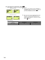
Number of parameter settings
Set the initial setting of A/D converter module and the parameter setting of auto refresh setting so that the number of
parameters, including these of other intelligent function modules, does not exceed the number of parameters that can
be set in the CPU module or the head module.
For the maximum number of parameters that can be set in the CPU module or the head module (maximum number of
parameter settings), refer to the following.
MELSEC-L CPU Module User's Manual (Hardware Design, Maintenance and Inspection)
MELSEC-L CC-Link IE Field Network Head Module User's Manual
(1) Number of A/D converter module parameters
For A/D converter modules, the following number of parameters can be set per module.
Initial setting
Auto refresh setting
L60AD4
Target module
12
75 (maximum number of settings)
L60ADVL8, L60ADIL8
8
37 (maximum number of settings)
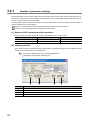
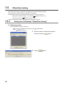
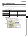
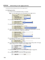
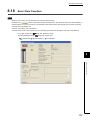
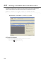
(2) Checking method
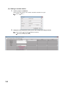
The maximum number of parameter settings and the number of parameter settings set for the intelligent function
module can be checked with the following operation.
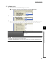
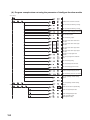
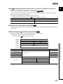
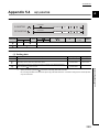
Project window
[Intelligent Function Module]
Right-click
[Intelligent Function Module Parameter List]
1)
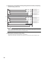
No.
1)
24
2)
3)
4)
Description
The total number of parameters in the initial settings selected on the dialog box
2)
The maximum number of parameter settings in the initial settings
3)
The total number of parameters in the auto refresh settings selected on the dialog box
4)
The maximum number of parameter settings in the auto refresh settings
CHAPTER 3 SPECIFICATIONS
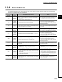
3.3
Function List
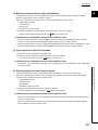
The following is the function list of the A/D converter module.
Applicable model
Item
Description
L60AD4
L60ADVL8,
L60ADIL8
Reference
Page 69, Section
8.2
Analog input values are converted into digital at every sampling cycle
and stored in the buffer memory as digital output values.
Page 69, Section
8.3 (1)
Time
average
A/D conversion is performed for a set period of time and averaging
processing is performed on the total value excluding the maximum
and the minimum values. The values obtained in averaging
processing are stored in the buffer memory. The number of processing
times within a set period of time changes depending on the number of
channels where A/D conversion is enabled.
Page 70, Section
8.3 (2) (a)
Count
average
A/D conversions are performed a set number of times and averaging
processing is performed on the total value excluding the maximum
and the minimum values. The values obtained in averaging
processing are stored in the buffer memory. The time taken for the
mean value calculated through average processing to be stored in the
buffer memory changes depending on the number of channels where
A/D conversion is enabled.
Page 71, Section
8.3 (2) (b)
Moving
average
The average of a specified number of digital output values is
calculated at every sampling cycle and is stored in the buffer memory.
Because the target set of values for averaging processing shifts to
another to involve a subsequent value at every sampling processing,
the latest digital output values can be always obtained.
Page 71, Section
8.3 (2) (c)
Range switching function
The input range to use can be selected from the following ranges:
• Factory default range (4 to 20mA, 0 to 20mA, 1 to 5V, 0 to 5V, -10 to
10V, 0 to 10V)
• User range
• Extended mode range (4 to 20mA (Extended mode), 1 to 5V
(Extended mode))
Page 54, Section
7.2
Conversion speed switch function
The conversion speed can be selected from 20µs, 80µs or 1ms.
Input range extension function
This function extends the input range of 4 to 20mA and that of 1 to 5V.
By combining this function with the input signal error detection
function, simple disconnection detection can be executed.
Page 74, Section
8.4
Maximum value/minimum value hold
function
This function stores the maximum digital value and minimum digital
output value in the buffer memory for each channel. When an
operation function such as the scaling function is used, the maximum
and minimum scaling values (digital operation values) are stored.
Page 76, Section
8.6
Input signal error detection function
This function outputs an alarm when the analog input value exceeds a
preset range.
Page 77, Section
8.7
Input signal error detection
extension function
The detection method of the input signal error detection function can
be extended. Use this function to detect the input signal error only in
the lower limit or upper limit, or to execute the disconnection detection.
Page 82, Section
8.8
Warning output function (process
alarm)
This function outputs alarm when a digital output value is in the range
set in advance. When an operation function such as the scaling
function is used, the scaling value (digital operation value) is the target
of detection.
Page 85, Section
8.9
Scaling function
The A/D converter module scale-converts the output digital value to
the set range of the scaling upper limit value and scaling lower limit
value. This omits the programming of the scale conversion.
Page 88, Section
8.10
Shift function
The A/D converter module adds the set shifting amount to conversion
value to the scaling value (digital operation value) and stores in the
buffer memory. Fine adjustment can be performed easily when the
system starts.
Sampling processing
A/D
conversion
method
Averaging
processing
×
×
Page 75, Section
8.5
Page 94, Section
8.11
25
3
3.3 Function List
Sets whether to enable or disable A/D conversion for each channel.
Disabling the A/D conversion for unused channels reduces the
conversion cycles.
A/D conversion enable/disable
function
Applicable model
Item
Description
L60AD4
L60ADVL8,
L60ADIL8
Reference
Digital clipping function
When the input voltage or current exceeds the input range, the
maximum value of the scaling value (digital operation value) can be
set to 20000, and the minimum value can be set to 0 or -20000.
×
Page 99, Section
8.12
Difference conversion function
This function subtracts the difference conversion reference value from
the scaling value (digital operation value) and stores the acquired
value in the buffer memory.
×
Page 103, Section
8.13
Logging function
This function logs the digital output value or scaling value (digital
operation value). The data of 10000 points can be logged for each
channel.
Flow amount integration function
This function converts analog values that are input to the A/D
converter module from a flow meter (a value obtained by converting
the instantaneous flow amount to a voltage value or current value) into
digital and integrates the digital values to calculate the flow amount in
a certain period of time.
Error log function
This function stores errors and alarms that occurred in the A/D
converter module in the buffer memory.
Sixteen errors and alarms in total can be stored.
Page 133, Section
8.16
Module error collection function
This function collects errors and alarms that occurred in the A/D
converter module and stores to the CPU module.
Page 136, Section
8.17
Error clear function
Clearing the error from the system monitor at error occurrence is
possible.
Page 137, Section
8.18
Saving and restoring offset/gain
values
The offset/gain value of the user range can be saved or restored.
Page 138, Section
8.19
Offset/gain setting
This function compensates for errors in digital output values.
Page 60, Section
7.5
*1
×
Page 108, Section
8.14
Page 123, Section
8.15
To use the logging function with the L60ADVL8 or L60ADIL8, use the data logging function of the CPU module.
For the data logging function of the CPU module, refer to the following.
QnUDVCPU/LCPU User's Manual (Data Logging Function)
26
*1
CHAPTER 3 SPECIFICATIONS
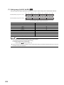
3.4
I/O Signal List
The following shows the list of the A/D converter module I/O signals.
For the details of I/O signals, refer to the followings.
• Details of I/O signals (
Page 192, Appendix 1)
Input signal
Device number
X0
Output signal
Signal name
Device number
Module READY
Y0
X1
Y1
X2
Y2
X3
X4
3
Signal name
Y3
Use prohibited
Y4
X5
Y5
X6
Y6
X7
Use prohibited
Y7
X8
Warning output signal
Y8
X9
Operating condition setting completed flag
Y9
Operating condition setting request
XA
Offset/gain setting mode flag
YA
User range write request
XB
Channel change completed flag
YB
Channel change request
XC
Input signal error detection signal
YC
Use prohibited
XD
Maximum value/minimum value reset completed
flag
YD
Maximum value/minimum value reset request
XE
A/D conversion completed flag
YE
Use prohibited
XF
Error flag
YF
Error clear request
● Do not use the "Use prohibited" signals shown above because the system uses them.
If users use (turn on) the signals, the functions of the A/D converter module cannot be guaranteed.
● The I/O signals are common in the A/D converter modules.
27
3.4 I/O Signal List
● The I/O number (X/Y) described above shows the case that the start I/O number of the A/D converter module is set to "0".
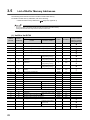
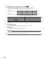
3.5
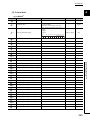
List of Buffer Memory Addresses
The following shows the list of the A/D converter module buffer memory.
For details of buffer memory addresses, refer to the following.
• Details of buffer memory addresses (
Page 199, Appendix 2)
Do not write data to the system areas and read-only areas in the buffer memory.
Writing data to these areas may lead the module to malfunction.
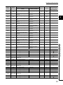
(1) Un\G0 to Un\G1799
Name
Address
(decimal)
Address
(hexadecimal)
0
0H
A/D conversion enable/disable setting
1
1H
2
28
L60AD4
L60ADVL8, L60ADIL8
Default
*1
*2
Read/Write
Item enabled by
turning on and off
Operating condition
setting request (Y9)
0000H
R/W
CH1 Time Average/ Count Average/Moving Average
0
R/W
2H
CH2 Time Average/ Count Average/Moving Average
0
R/W
3
3H
CH3 Time Average/ Count Average/Moving Average
0
R/W
4
4H
CH4 Time Average/ Count Average/Moving Average
0
R/W
5
5H
System area
CH5 Time Average/ Count
Average/Moving Average
0
R/W
6
6H
System area
CH6 Time Average/ Count
Average/Moving Average
0
R/W
7
7H
System area
CH7 Time Average/ Count
Average/Moving Average
0
R/W
8
8H
System area
CH8 Time Average/ Count
Average/Moving Average
0
R/W
9
9H
Averaging process setting (used to replace Q64AD, Q68ADV,
Q68ADI)
0000H
R/W
10
AH
A/D conversion completed flag
0000H
R
11
BH
CH1 Digital output value
0
R
12
CH
CH2 Digital output value
0
R
13
DH
CH3 Digital output value
0
R
14
EH
CH4 Digital output value
0
R
15
FH
System area
CH5 Digital output value
0
R
16
10H
System area
CH6 Digital output value
0
R
17
11H
System area
CH7 Digital output value
0
R
18
12H
System area
CH8 Digital output value
0
R
19
13H
Latest error code
20
14H
Setting range (CH1 to CH4)
21
15H
System area
Setting range (CH5 to CH8)
0
R
0000H
R
0000H
R
22
16H
Offset/gain setting mode Offset specification
0000H
R/W
23
17H
Offset/gain setting mode Gain specification
0000H
R/W
24
18H
Averaging process setting (CH1 to CH4)
25
19H
System area
Averaging process setting
(CH5 to CH8)
26
1AH
Conversion speed setting
System area
27
1BH
Input signal error detection extension setting (CH1 to CH4)
0000H
R/W
0000H
R/W
0001H
R/W
0000H
R/W
CHAPTER 3 SPECIFICATIONS
Name
Item enabled by
turning on and off
Operating condition
setting request (Y9)
Address
(decimal)
Address
(hexadecimal)
28
1CH
System area
Input signal error detection
extension setting (CH5 to
CH8)
0000H
R/W
29
1DH
Digital clipping enable/disable
setting
System area
000FH
R/W
30
1EH
CH1 Maximum value
0
R
31
1FH
CH1 Minimum value
0
R
*1
L60AD4
L60ADVL8, L60ADIL8
Default
Read/Write
*2
32
20H
CH2 Maximum value
0
R
33
21H
CH2 Minimum value
0
R
34
22H
CH3 Maximum value
0
R
35
23H
CH3 Minimum value
0
R
36
24H
CH4 Maximum value
0
R
37
25H
CH4 Minimum value
0
R
38
26H
System area
CH5 Maximum value
0
R
39
27H
System area
CH5 Minimum value
0
R
40
28H
System area
CH6 Maximum value
0
R
41
29H
System area
CH6 Minimum value
0
R
42
2AH
System area
CH7 Maximum value
0
R
43
2BH
System area
CH7 Minimum value
0
R
44
2CH
System area
CH8 Maximum value
0
R
45
2DH
System area
CH8 Minimum value
0
R
46
2EH
System area
47
2FH
000FH
(AD4)
00FFH
(ADL8)
Input signal error detection setting
3
R/W
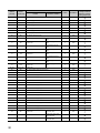
3.5 List of Buffer Memory Addresses
*3
48
30H
000FH
(AD4)
00FFH
(ADL8)
Warning output setting
R/W
*3
31H
Input signal error detection flag
0000H
R
50
32H
Warning output flag (Process alarm)
0000H
R
51
33H
52
34H
49
53
35H
System area
000FH
(AD4)
00FFH
(ADL8)
Scaling enable/disable setting
R/W
*3
54
36H
CH1 Scaling value (digital operation value)
0
R
55
37H
CH2 Scaling value (digital operation value)
0
R
56
38H
CH3 Scaling value (digital operation value)
0
R
57
39H
CH4 Scaling value (digital operation value)
0
R
0
R
58
3AH
System area
CH5 Scaling value (digital
operation value)
59
3BH
System area
CH6 Scaling value (digital
operation value)
0
R
60
3CH
System area
CH7 Scaling value (digital
operation value)
0
R
61
3DH
System area
CH8 Scaling value (digital
operation value)
0
R
29
Name
Address
(decimal)
Address
(hexadecimal)
62
3EH
CH1 Scaling lower limit value
0
R/W
63
3FH
CH1 Scaling upper limit value
0
R/W
64
40H
CH2 Scaling lower limit value
0
R/W
65
41H
CH2 Scaling upper limit value
0
R/W
66
42H
CH3 Scaling lower limit value
0
R/W
67
43H
CH3 Scaling upper limit value
0
R/W
68
44H
CH4 Scaling lower limit value
0
R/W
69
45H
CH4 Scaling upper limit value
0
R/W
70
46H
System area
CH5 Scaling lower limit
value
0
R/W
71
47H
System area
CH5 Scaling upper limit
value
0
R/W
72
48H
System area
CH6 Scaling lower limit
value
0
R/W
73
49H
System area
CH6 Scaling upper limit
value
0
R/W
74
4AH
System area
CH7 Scaling lower limit
value
0
R/W
75
4BH
System area
CH7 Scaling upper limit
value
0
R/W
76
4CH
System area
CH8 Scaling lower limit
value
0
R/W
77
4DH
System area
CH8 Scaling upper limit
value
0
R/W
78 to 85
4EH to 55H
System area
86
56H
CH1 Process alarm lower lower limit value
0
R/W
87
57H
CH1 Process alarm lower upper limit value
0
R/W
88
58H
CH1 Process alarm upper lower limit value
0
R/W
89
59H
CH1 Process alarm upper upper limit value
0
R/W
90
5AH
CH2 Process alarm lower lower limit value
0
R/W
91
5BH
CH2 Process alarm lower upper limit value
0
R/W
92
5CH
CH2 Process alarm upper lower limit value
0
R/W
93
5DH
CH2 Process alarm upper upper limit value
0
R/W
94
5EH
CH3 Process alarm lower lower limit value
0
R/W
95
5FH
CH3 Process alarm lower upper limit value
0
R/W
96
60H
CH3 Process alarm upper lower limit value
0
R/W
97
61H
CH3 Process alarm upper upper limit value
0
R/W
98
62H
CH4 Process alarm lower lower limit value
0
R/W
99
63H
CH4 Process alarm lower upper limit value
0
R/W
100
64H
CH4 Process alarm upper lower limit value
0
R/W
101
65H
CH4 Process alarm upper upper limit value
0
R/W
102
66H
System area
CH5 Process alarm lower
lower limit value
0
R/W
103
67H
System area
CH5 Process alarm lower
upper limit value
0
R/W
104
68H
System area
CH5 Process alarm upper
lower limit value
0
R/W
30
L60AD4
L60ADVL8, L60ADIL8
Default
*1
*2
Read/Write
Item enabled by
turning on and off
Operating condition
setting request (Y9)
CHAPTER 3 SPECIFICATIONS
Name
Address
(decimal)
Address
(hexadecimal)
105
69H
System area
CH5 Process alarm upper
upper limit value
0
R/W
106
6AH
System area
CH6 Process alarm lower
lower limit value
0
R/W
107
6BH
System area
CH6 Process alarm lower
upper limit value
0
R/W
0
R/W
*1
L60AD4
L60ADVL8, L60ADIL8
Default
Read/Write
*2
Item enabled by
turning on and off
Operating condition
setting request (Y9)
3
108
6CH
System area
CH6 Process alarm upper
lower limit value
109
6DH
System area
CH6 Process alarm upper
upper limit value
0
R/W
110
6EH
System area
CH7 Process alarm lower
lower limit value
0
R/W
111
6FH
System area
CH7 Process alarm lower
upper limit value
0
R/W
112
70H
System area
CH7 Process alarm upper
lower limit value
0
R/W
113
71H
System area
CH7 Process alarm upper
upper limit value
0
R/W
114
72H
System area
CH8 Process alarm lower
lower limit value
0
R/W
115
73H
System area
CH8 Process alarm lower
upper limit value
0
R/W
116
74H
System area
CH8 Process alarm upper
lower limit value
0
R/W
117
75H
System area
CH8 Process alarm upper
upper limit value
0
R/W
118 to 141
76H to 8DH
System area
142
8EH
CH1 Input signal error detection setting value
50
R/W
143
8FH
CH2 Input signal error detection setting value
50
R/W
144
90H
CH3 Input signal error detection setting value
50
R/W
145
91H
CH4 Input signal error detection setting value
50
R/W
146
92H
System area
CH5 Input signal error
detection setting value
50
R/W
147
93H
System area
CH6 Input signal error
detection setting value
50
R/W
148
94H
System area
CH7 Input signal error
detection setting value
50
R/W
149
95H
System area
CH8 Input signal error
detection setting value
50
R/W
150
96H
CH1 Shifting amount to conversion
value
System area
0
R/W
151
97H
CH2 Shifting amount to conversion
value
System area
0
R/W
152
98H
CH3 Shifting amount to conversion
value
System area
0
R/W
153
99H
CH4 Shifting amount to conversion
value
System area
0
R/W
154 to 157
9AH to 9DH
System area
158
9EH
159
9FH
Mode switching setting
0
R/W
160 to 171
A0H to ABH
172
ACH
173
ADH
CH2 Difference conversion trigger
System area
0
R/W
174
AEH
CH3 Difference conversion trigger
System area
0
R/W
System area
3.5 List of Buffer Memory Addresses
System area
CH1 Difference conversion trigger
0
R/W
31
Name
Address
(decimal)
Address
(hexadecimal)
L60AD4
L60ADVL8, L60ADIL8
Default
*1
*2
Read/Write
Item enabled by
turning on and off
Operating condition
setting request (Y9)
0
R/W
System area
0
R
CH2 Difference conversion
reference value
System area
0
R
B6H
CH3 Difference conversion
reference value
System area
0
R
183
B7H
CH4 Difference conversion
reference value
System area
0
R
184 to 189
B8H to BDH
175
AFH
176 to 179
B0H to B3H
CH4 Difference conversion trigger
180
B4H
CH1 Difference conversion
reference value
181
B5H
182
System area
System area
System area
190
BEH
CH1 Difference conversion status
flag
191
BFH
CH2 Difference conversion status
flag
System area
0
R
192
C0H
CH3 Difference conversion status
flag
System area
0
R
193
C1H
CH4 Difference conversion status
flag
System area
0
R
194 to 199
C2H to C7H
200
C8H
Pass data classification setting
201
C9H
System area
202
CAH
CH1 Industrial shipment settings
offset value (L)
203
CBH
204
32
System area
0
R
System area
System area
0
R/W
CH1 Industrial shipment
settings offset value
0
R/W
CH1 Industrial shipment settings
offset value (H)
CH1 Industrial shipment
settings gain value
0
R/W
CCH
CH1 Industrial shipment settings
gain value (L)
CH2 Industrial shipment
settings offset value
0
R/W
205
CDH
CH1 Industrial shipment settings
gain value (H)
CH2 Industrial shipment
settings gain value
0
R/W
206
CEH
CH2 Industrial shipment settings
offset value (L)
CH3 Industrial shipment
settings offset value
0
R/W
207
CFH
CH2 Industrial shipment settings
offset value (H)
CH3 Industrial shipment
settings gain value
0
R/W
208
D0H
CH2 Industrial shipment settings
gain value (L)
CH4 Industrial shipment
settings offset value
0
R/W
209
D1H
CH2 Industrial shipment settings
gain value (H)
CH4 Industrial shipment
settings gain value
0
R/W
210
D2H
CH3 Industrial shipment settings
offset value (L)
CH5 Industrial shipment
settings offset value
0
R/W
211
D3H
CH3 Industrial shipment settings
offset value (H)
CH5 Industrial shipment
settings gain value
0
R/W
212
D4H
CH3 Industrial shipment settings
gain value (L)
CH6 Industrial shipment
settings offset value
0
R/W
213
D5H
CH3 Industrial shipment settings
gain value (H)
CH6 Industrial shipment
settings gain value
0
R/W
214
D6H
CH4 Industrial shipment settings
offset value (L)
CH7 Industrial shipment
settings offset value
0
R/W
215
D7H
CH4 Industrial shipment settings
offset value (H)
CH7 Industrial shipment
settings gain value
0
R/W
216
D8H
CH4 Industrial shipment settings
gain value (L)
CH8 Industrial shipment
settings offset value
0
R/W
217
D9H
CH4 Industrial shipment settings
gain value (H)
CH8 Industrial shipment
settings gain value
0
R/W
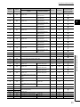
CHAPTER 3 SPECIFICATIONS
Name
Item enabled by
turning on and off
Operating condition
setting request (Y9)
Address
(hexadecimal)
218
DAH
CH1 User range settings offset
value (L)
CH1 User range settings
offset value
0
R/W
219
DBH
CH1 User range settings offset
value (H)
CH1 User range settings
gain value
0
R/W
220
DCH
CH1 User range settings gain value
(L)
CH2 User range settings
offset value
0
R/W
221
DDH
CH1 User range settings gain value
(H)
CH2 User range settings
gain value
0
R/W
222
DEH
CH2 User range settings offset
value (L)
CH3 User range settings
offset value
0
R/W
223
DFH
CH2 User range settings offset
value (H)
CH3 User range settings
gain value
0
R/W
224
E0H
CH2 User range settings gain value
(L)
CH4 User range settings
offset value
0
R/W
225
E1H
CH2 User range settings gain value
(H)
CH4 User range settings
gain value
0
R/W
226
E2H
CH3 User range settings offset
value (L)
CH5 User range settings
offset value
0
R/W
227
E3H
CH3 User range settings offset
value (H)
CH5 User range settings
gain value
0
R/W
228
E4H
CH3 User range settings gain value
(L)
CH6 User range settings
offset value
0
R/W
229
E5H
CH3 User range settings gain value
(H)
CH6 User range settings
gain value
0
R/W
230
E6H
CH4 User range settings offset
value (L)
CH7 User range settings
offset value
0
R/W
231
E7H
CH4 User range settings offset
value (H)
CH7 User range settings
gain value
0
R/W
232
E8H
CH4 User range settings gain value
(L)
CH8 User range settings
offset value
0
R/W
233
E9H
CH4 User range settings gain value
(H)
CH8 User range settings
gain value
0
R/W
234 to 999
EAH to 3E7H
1000
3E8H
CH1 Logging enable/disable setting
System area
1
R/W
1001
3E9H
CH2 Logging enable/disable setting
System area
1
R/W
1002
3EAH
CH3 Logging enable/disable setting
System area
1
R/W
CH4 Logging enable/disable setting
System area
1
R/W
*1
L60AD4
L60ADVL8, L60ADIL8
System area
Default
Read/Write
*2
1003
3EBH
1004 to
1007
3ECH to 3EFH
1008
3F0H
CH1 Logging hold request
System area
0
R/W
1009
3F1H
CH2 Logging hold request
System area
0
R/W
1010
3F2H
CH3 Logging hold request
System area
0
R/W
1011
3F3H
CH4 Logging hold request
System area
0
R/W
1012 to
1015
3F4H to 3F7H
System area
System area
1016
3F8H
CH1 Logging hold flag
System area
0
R
1017
3F9H
CH2 Logging hold flag
System area
0
R
1018
3FAH
CH3 Logging hold flag
System area
0
R
CH4 Logging hold flag
System area
0
R
1019
3FBH
1020 to
1023
3FCH to 3FFH
1024
400H
CH1 Logging data setting
System area
1
R/W
1025
401H
CH2 Logging data setting
System area
1
R/W
System area
3
3.5 List of Buffer Memory Addresses
Address
(decimal)
33
Name
Item enabled by
turning on and off
Operating condition
setting request (Y9)
Address
(decimal)
Address
(hexadecimal)
1026
402H
CH3 Logging data setting
System area
1
R/W
1027
403H
CH4 Logging data setting
System area
1
R/W
1028 to
1031
404H to 407H
1032
408H
CH1 Logging cycle setting value
System area
4
R/W
1033
409H
CH2 Logging cycle setting value
System area
4
R/W
1034
40AH
CH3 Logging cycle setting value
System area
4
R/W
1035
40BH
CH4 Logging cycle setting value
System area
4
R/W
1036 to
1039
40CH to 40FH
1040
410H
CH1 Logging cycle unit setting
System area
1
R/W
1041
411H
CH2 Logging cycle unit setting
System area
1
R/W
1042
412H
CH3 Logging cycle unit setting
System area
1
R/W
1043
413H
CH4 Logging cycle unit setting
System area
1
R/W
1044 to
1047
414H to 417H
1048
418H
CH1 Logging points after trigger
System area
5000
R/W
1049
419H
CH2 Logging points after trigger
System area
5000
R/W
1050
41AH
CH3 Logging points after trigger
System area
5000
R/W
1051
41BH
CH4 Logging points after trigger
System area
5000
R/W
1052 to
1055
41CH to 41FH
1056
420H
CH1 Level trigger condition setting
System area
0
R/W
1057
421H
CH2 Level trigger condition setting
System area
0
R/W
1058
422H
CH3 Level trigger condition setting
System area
0
R/W
1059
423H
CH4 Level trigger condition setting
System area
0
R/W
1060 to
1063
424H to 427H
1064
428H
CH1 Trigger data
System area
54
R/W
1065
429H
CH2 Trigger data
System area
55
R/W
1066
42AH
CH3 Trigger data
System area
56
R/W
1067
42BH
CH4 Trigger data
System area
57
R/W
1068 to
1071
42CH to 42FH
System area
1072
430H
Level data 0
System area
0
R/W
1073
431H
Level data 1
System area
0
R/W
1074
432H
Level data 2
System area
0
R/W
1075
433H
Level data 3
System area
0
R/W
1076
434H
Level data 4
System area
0
R/W
1077
435H
Level data 5
System area
0
R/W
1078
436H
Level data 6
System area
0
R/W
1079
437H
Level data 7
System area
0
R/W
1080
438H
Level data 8
System area
0
R/W
1081
439H
Level data 9
System area
0
R/W
1082
43AH
CH1 Trigger setting value
System area
0
R/W
1083
43BH
CH2 Trigger setting value
System area
0
R/W
34
L60AD4
L60ADVL8, L60ADIL8
System area
System area
System area
System area
System area
Default
*1
*2
Read/Write
CHAPTER 3 SPECIFICATIONS
Name
Address
(decimal)
Address
(hexadecimal)
1084
43CH
CH3 Trigger setting value
System area
0
R/W
1085
43DH
CH4 Trigger setting value
System area
0
R/W
1086 to
1089
43EH to 441H
*1
L60AD4
L60ADVL8, L60ADIL8
System area
Default
Read/Write
*2
Item enabled by
turning on and off
Operating condition
setting request (Y9)
1090
442H
CH1 Head pointer
System area
0
R
1091
443H
CH2 Head pointer
System area
0
R
1092
444H
CH3 Head pointer
System area
0
R
1093
445H
CH4 Head pointer
System area
0
R
1094 to
1097
446H to 449H
1098
44AH
0
R
System area
CH1 Latest pointer
System area
1099
44BH
CH2 Latest pointer
System area
0
R
1100
44CH
CH3 Latest pointer
System area
0
R
1101
44DH
CH4 Latest pointer
System area
0
R
1102 to 1105
44EH to 451H
1106
452H
CH1 Number of logging data
System area
0
R
1107
453H
CH2 Number of logging data
System area
0
R
System area
454H
CH3 Number of logging data
System area
0
R
455H
CH4 Number of logging data
System area
0
R
1110 to 1113
456H to 459H
1114
45AH
CH1 Trigger pointer
System area
0
R
1115
45BH
CH2 Trigger pointer
System area
0
R
1116
45CH
CH3 Trigger pointer
System area
0
R
1117
45DH
CH4 Trigger pointer
System area
0
R
1118 to 1121
45EH to 461H
1122
462H
1123
463H
System area
System area
CH1 Logging cycle
monitor value
(s)
System area
0
R
(ms)
System area
0
R
1124
464H
(µs)
System area
0
R
1125
465H
(s)
System area
0
R
1126
466H
(ms)
System area
0
R
CH2 Logging cycle
monitor value
1127
467H
(µs)
System area
0
R
1128
468H
(s)
System area
0
R
1129
469H
(ms)
System area
0
R
CH3 Logging cycle
monitor value
1130
46AH
(µs)
System area
0
R
1131
46BH
(s)
System area
0
R
1132
46CH
(ms)
System area
0
R
1133
46DH
(µs)
System area
0
R
1134 to 1153
46EH to 481H
1154
482H
0
R
1155
483H
1156
484H
1157
485H
CH4 Logging cycle
monitor value
System area
CH1 Trigger
detection
time
First two
digits of
the year
Last two
digits of
the year
System area
Month
Day
System area
0
R
Hour
Minute
System area
0
R
Second
Day of
the week
System area
0
R
3.5 List of Buffer Memory Addresses
1108
1109
3
35
Name
Address
(decimal)
Address
(hexadecimal)
1158
486H
1159
487H
1160
488H
L60AD4
CH2 Trigger
detection
time
L60ADVL8, L60ADIL8
Default
*1
*2
Read/Write
Item enabled by
turning on and off
Operating condition
setting request (Y9)
First two
digits of
the year
Last two
digits of
the year
System area
0
R
Month
Day
System area
0
R
Hour
Minute
System area
0
R
System area
0
R
1161
489H
Second
Day of
the week
1162
48AH
First two
digits of
the year
Last two
digits of
the year
System area
0
R
1163
48BH
Month
Day
System area
0
R
1164
48CH
Hour
Minute
System area
0
R
System area
0
R
CH3 Trigger
detection
time
1165
48DH
Second
Day of
the week
1166
48EH
First two
digits of
the year
Last two
digits of
the year
System area
0
R
1167
48FH
Month
Day
System area
0
R
1168
490H
Hour
Minute
System area
0
R
Second
Day of
the week
System area
0
R
1169
491H
1170 to 1299
492H to 513H
CH4 Trigger
detection
time
System area
1300
514H
CH1 Flow amount integration
enable/disable setting
1301
515H
CH2 Flow amount integration
enable/disable setting
System area
1
R/W
1302
516H
CH3 Flow amount integration
enable/disable setting
System area
1
R/W
1303
517H
CH4 Flow amount integration
enable/disable setting
System area
1
R/W
1304 to
1307
518H to 51BH
1308
51CH
CH1 Integration cycle setting
System area
4
R/W
1309
51DH
CH2 Integration cycle setting
System area
4
R/W
1310
51EH
CH3 Integration cycle setting
System area
4
R/W
1311
51FH
CH4 Integration cycle setting
System area
4
R/W
1312 to
1315
520H to 523H
1316
524H
CH1 Flow amount time unit setting
System area
0
R/W
1317
525H
CH2 Flow amount time unit setting
System area
0
R/W
1318
526H
CH3 Flow amount time unit setting
System area
0
R/W
1319
527H
CH4 Flow amount time unit setting
System area
0
R/W
1320 to
1323
528H to 52BH
1324
52CH
CH1 Unit scaling setting
System area
0
R/W
1325
52DH
CH2 Unit scaling setting
System area
0
R/W
1326
52EH
CH3 Unit scaling setting
System area
0
R/W
1327
52FH
CH4 Unit scaling setting
System area
0
R/W
1328 to
1331
530H to 533H
1332
534H
0
R
36
System area
1
R/W
System area
System area
System area
System area
CH1 Integrated flow amount (L)
System area
CHAPTER 3 SPECIFICATIONS
Name
Address
(decimal)
Address
(hexadecimal)
*1
L60AD4
L60ADVL8, L60ADIL8
Default
Read/Write
*2
Item enabled by
turning on and off
Operating condition
setting request (Y9)
1333
535H
CH1 Integrated flow amount (H)
System area
0
R
1334
536H
CH2 Integrated flow amount (L)
System area
0
R
1335
537H
CH2 Integrated flow amount (H)
System area
0
R
1336
538H
CH3 Integrated flow amount (L)
System area
0
R
1337
539H
CH3 Integrated flow amount (H)
System area
0
R
1338
53AH
CH4 Integrated flow amount (L)
System area
0
R
CH4 Integrated flow amount (H)
System area
0
R
System area
0
R
1339
53BH
1340 to
1347
53CH to 543H
1348
544H
System area
CH1 Integration cycle monitor value
545H
CH2 Integration cycle monitor value
System area
0
R
546H
CH3 Integration cycle monitor value
System area
0
R
1351
547H
CH4 Integration cycle monitor value
System area
0
R
1352 to
1355
548H to 54BH
1356
54CH
CH1 Flow amount integration
temporary stop request
System area
0
R/W
1357
54DH
CH2 Flow amount integration
temporary stop request
System area
0
R/W
1358
54EH
CH3 Flow amount integration
temporary stop request
System area
0
R/W
1359
54FH
CH4 Flow amount integration
temporary stop request
System area
0
R/W
1360 to
1363
550H to 553H
1364
554H
CH1 Flow amount integration
temporary stop flag
System area
0
R
1365
555H
CH2 Flow amount integration
temporary stop flag
System area
0
R
1366
556H
CH3 Flow amount integration
temporary stop flag
System area
0
R
1367
557H
CH4 Flow amount integration
temporary stop flag
System area
0
R
1368 to
1371
558H to 55BH
1372
55CH
CH1 Integrated flow amount clear
request
System area
0
R/W
1373
55DH
CH2 Integrated flow amount clear
request
System area
0
R/W
1374
55EH
CH3 Integrated flow amount clear
request
System area
0
R/W
1375
55FH
CH4 Integrated flow amount clear
request
System area
0
R/W
1376 to
1379
560H to 563H
1380
564H
CH1 Integrated flow amount clear
flag
System area
0
R
1381
565H
CH2 Integrated flow amount clear
flag
System area
0
R
1382
566H
CH3 Integrated flow amount clear
flag
System area
0
R
1383
567H
CH4 Integrated flow amount clear
flag
System area
0
R
1384 to
1699
568H to 6A3H
System area
System area
System area
System area
System area
3.5 List of Buffer Memory Addresses
1349
1350
3
37
Name
Address
(decimal)
Address
(hexadecimal)
L60AD4
L60ADVL8, L60ADIL8
Default
*1
*2
Read/Write
Item enabled by
turning on and off
Operating condition
setting request (Y9)
1700
6A4H
System area
CH1 A/D conversion status
0
R
1701
6A5H
System area
CH2 A/D conversion status
0
R
1702
6A6H
System area
CH3 A/D conversion status
0
R
1703
6A7H
System area
CH4 A/D conversion status
0
R
1704
6A8H
System area
CH5 A/D conversion status
0
R
1705
6A9H
System area
CH6 A/D conversion status
0
R
1706
6AAH
System area
CH7 A/D conversion status
0
R
1707
6ABH
System area
CH8 A/D conversion status
0
R
1708
6ACH
1709
6ADH
1710
6AEH
System area
System area
CH1 Analog input monitor
0
R
0
R
1711
6AFH
System area
CH1 Analog input monitor
unit
1712
6B0H
System area
CH2 Analog input monitor
0
R
0
R
1713
6B1H
System area
CH2 Analog input monitor
unit
1714
6B2H
System area
CH3 Analog input monitor
0
R
0
R
1715
6B3H
System area
CH3 Analog input monitor
unit
1716
6B4H
System area
CH4 Analog input monitor
0
R
1717
6B5H
System area
CH4 Analog input monitor
unit
0
R
1718
6B6H
System area
CH5 Analog input monitor
0
R
0
R
1719
6B7H
System area
CH5 Analog input monitor
unit
1720
6B8H
System area
CH6 Analog input monitor
0
R
0
R
1721
6B9H
System area
CH6 Analog input monitor
unit
1722
6BAH
System area
CH7 Analog input monitor
0
R
0
R
1723
6BBH
System area
CH7 Analog input monitor
unit
1724
6BCH
System area
CH8 Analog input monitor
0
R
1725
6BDH
System area
CH8 Analog input monitor
unit
0
R
1726 to
1799
6BEH to 707H
System area
*1
*2
*3
38
The default value is a value set after power-on or after resetting the CPU module.
This shows whether read or write from programs is possible.
R: Readable
W: Writable
(AD4) indicates the L60AD4. (ADL8) indicates the L60ADVL8 and L60ADIL8.
CHAPTER 3 SPECIFICATIONS
(2) Error history (Un\G1800 to Un\G4999)
This area is common to L60AD4, L60ADVL8, and L60ADIL8.
Address
(decimal)
Address
(hexadecimal)
1800
708H
1801 to
1809
709H to 711H
1810
712H
1811
713H
1812
714H
1813
715H
Default*1
Read/Write *2
Item enabled by
turning on and off
Operating condition
setting request (Y9)
Latest address of error history
0
R
System area
0
R
Name
Error code
No.1
Error time
First two digits
of the year
Last two digits
of the year
0
R
Month
Day
0
R
Hour
Minute
0
R
Second
Day of the
week
0
R
716H
1815 to
1819
717H to 71BH
1820 to
1829
71CH to 725H
No.2
Same as No. 1
1830 to
1839
726H to 72FH
No.3
Same as No. 1
1840 to
1849
730H to 739H
No.4
Same as No. 1
1850 to
1859
73AH to 743H
No.5
Same as No. 1
1860 to
1869
744H to 74DH
No.6
Same as No. 1
1870 to
1879
74EH to 757H
No.7
Same as No. 1
1880 to
1889
758H to 761H
No.8
Same as No. 1
1890 to
1899
762H to 76BH
No.9
Same as No. 1
1900 to
1909
76CH to 775H
No.10
Same as No. 1
1910 to
1919
776H to 77FH
No.11
Same as No. 1
1920 to
1929
780H to 789H
No.12
Same as No. 1
1930 to
1939
78AH to 793H
No.13
Same as No. 1
1940 to
1949
794H to 79DH
No.14
Same as No. 1
1950 to
1959
79EH to 7A7H
No.15
Same as No. 1
1960 to
1969
7A8H to 7B1H
No.16
Same as No. 1
1970 to
4999
7B2H to 1387H
System area
*1
*2
System area
3.5 List of Buffer Memory Addresses
1814
3
The default value is a value set after power-on or after resetting the CPU module.
This shows whether read or write from programs is possible.
R: Readable
W: Writable
39
(3) Logging section (Un\G5000 to Un\G61439)
Name
Default*1
Read/Write*2
Item enabled by
turning on and off
Operating condition
setting request (Y9)
System area
0
R
CH2 Logging data
System area
0
R
61A8H to
88B7H
CH3 Logging data
System area
0
R
35000 to
44999
88B8H to
AFC7H
CH4 Logging data
System area
0
R
45000 to
61439
AFC8H to
EFFFH
System area
Address
(decimal)
Address
(hexadecimal)
5000 to
14999
1388H to
3A97H
CH1 Logging data
15000 to
24999
3A98H to
61A7H
25000 to
34999
*1
*2
40
L60AD4
L60ADVL8, L60ADIL8
The default value is a value set after power-on or after resetting the CPU module.
This shows whether read or write from programs is possible.
R: Readable
W: Writable
CHAPTER 4 PROCEDURES BEFORE STARTING THE OPERATION
CHAPTER 4
PROCEDURES BEFORE STARTING
THE OPERATION
This chapter describes the procedures before starting the operation.
Start
4
Connecting a module
Connect the A/D converter module in any desired
configuration.
Wiring
Perform wiring of external devices to the A/D
converter module.
For the connection of the module, refer to the
following.
•
Page 43, Section 5.1
For the wiring, refer to the following.
Is user range necessary?
NO
•
Page 51, Section 6.4
For the offset/gain setting, refer to the following.
•
Page 60, Section 7.5
YES
Offset/gain setting
To use user range, set the offset/gain values.
Programming and debugging
Creates and checks a program.
41
Memo
42
CHAPTER 5 SYSTEM CONFIGURATION
CHAPTER 5
SYSTEM CONFIGURATION
This chapter describes the overall configuration, number of connectable modules, and compatible software version of
the A/D converter module.
5.1
Overall System Configuration
The following shows a system configuration example for using the A/D converter module.
(1) When connected to a CPU module
5
Display unit
(optional)
Power supply module
CPU module
A/D converter module
I/O module or
intelligent function
module
END cover
5.1 Overall System Configuration
(2) When connected to a head module
Power supply module
Head module
A/D converter module
I/O module or
intelligent function
module
END cover
43
5.2
Applicable System
(1) Number of connectable modules
For the number of connectable modules, refer to the following.
MELSEC-L CPU Module User's Manual (Hardware Design, Maintenance and Inspection)
MELSEC-L CC-Link IE Field Network Head Module User's Manual
(2) Compatible software version
For the compatible software versions, refer to the following.
(a) L60AD4
Software
Version
GX Works2
Version 1.20W or later
GX Developer
Version 8.88S or later
GX Configurator-AD
Version 2.11M or later
(b) L60ADVL8, L60ADIL8
Software
5.3
Version
GX Works2
Version 1.513K or later
GX Developer
Version 8.88S or later
GX Configurator-AD
Not applicable
Restrictions When A/D Converter Module is Connected
to Head Module
The following describes the restriction when the A/D converter module is connected to a head module.
• Dedicated instruction cannot be used.
44
CHAPTER 6 INSTALLATION AND WIRING
CHAPTER 6
INSTALLATION AND WIRING
This chapter describes the installation and wiring of the A/D converter module.
6.1
Installation Environment and Installation Position
For precautions for installation environment and installation position, refer to the following.
MELSEC-L CPU Module User's Manual (Hardware Design, Maintenance and Inspection)
MELSEC-L CC-Link IE Field Network Head Module User's Manual
6
6.1 Installation Environment and Installation Position
45
6.2
Terminal Block
(1) Precautions
Tighten the terminal block screws within the following specified torque range.
Screw type
Tightening torque range
Terminal screw (M3 screw)
0.42 to 0.58N m
Terminal block mounting screw (M3.5 screw)
0.66 to 0.89N m
The table below shows applicable solderless terminals connected to the terminal block. When wiring, use
applicable wires and an appropriate tightening torque. Use UL-approved solderless terminals and, for
processing, use a tool recommended by their manufacturer. Also, sleeved solderless terminals cannot be used.
Solderless terminal
Wire
Model
Tightening torque
Diameter
Type
Material
Temperature rating
R1.25-3
0.42 to 0.58N m
AWG 22 to AWG 18
Stranded
Copper
75°C or more
(2) Signal names of the terminal block
The following shows signal names of the terminal block.
(a) L60AD4
Terminal block
Pin number
Signal name
1
V+
2
V-/ICH1
CH1
V-/ISLD
CH2
V-/ISLD
CH3
V-/ISLD
CH4
V-/ISLD
CH1
V+
CH1
I+
CH2
V+
CH2
I+
CH3
V+
CH3
I+
CH4
V+
CH4
I+
AG
FG
46
3
I+
4
SLD
5
V+
6
V-/ICH2
7
I+
8
SLD
9
V+
10
V-/ICH3
11
I+
12
SLD
13
V+
14
V-/ICH4
15
I+
16
SLD
17
AG
18
FG
CHAPTER 6 INSTALLATION AND WIRING
(b) L60ADVL8
Terminal block
Pin number
Signal name
1
V+
CH1
2
V-
3
V+
CH2
4
V-
5
CH1
VCH2
VCH3
VCH4
VCH5
VCH6
VCH7
VCH8
V-
CH1
V+
6
CH2
V+
7
CH3
V+
8
CH4
V+
CH5
V+
VV+
CH5
10
V-
11
V+
6
CH6
CH7
V+
13
FG
V+
9
12
AG
V-
CH4
CH6
V+
CH8
V+
V+
CH3
VV+
CH7
14
V-
15
V+
CH8
16
V-
17
AG
18
FG
Pin number
Signal name
Terminal block
1
6.2 Terminal Block
(c) L60ADIL8
I+
CH1
2
I-
3
I+
CH2
4
I-
5
CH1
ICH2
ICH3
ICH4
ICH5
ICH6
ICH7
ICH8
IFG
CH1
I+
6
CH2
I+
7
CH3
I+
8
CH4
I+
CH5
I+
I+
I-
9
I+
CH5
10
I-
11
I+
CH6
12
CH7
I+
13
AG
I-
CH4
CH6
I+
CH8
I+
I+
CH3
II+
CH7
14
I-
15
I+
CH8
16
I-
17
AG
18
FG
47
(3) Removal and installation of the terminal block
The following shows how to remove and install the terminal block.
(a) Removal procedure
1.
Open the terminal cover and loosen the terminal
block mounting screw.
Terminal block
mounting screw
2.
Using the terminal block fixing holes as a fulcrum,
remove the terminal block.
(b) Installation procedure
Terminal block fixing hole
1.
Fully insert the projections on the top of the
terminal block into the terminal block fixing holes
and press the terminal block until it snaps into
place.
2.
Open the terminal cover and tighten the terminal
block mounting screw.
Terminal block
mounting screw
48
CHAPTER 6 INSTALLATION AND WIRING
6.3
Wiring
(1) Wiring to a terminal block
The following shows wirings to a terminal block.
(a) L60AD4
• For the voltage input
CH1
CH1
V-/I-
CH1
V+
CH1
I+
SLD
CH2
CH2
V-/I-
CH2
V+
CH2
I+
6
SLD
CH3
CH3
V-/I-
CH3
V+
CH3
I+
SLD
CH4
CH4
V-/I-
CH4
V+
CH4
I+
SLD
AG
6.3 Wiring
FG
• For the current input
CH1
CH1
V-/I-
CH1
V+
CH1
I+
SLD
CH2
CH2
V-/I-
CH2
V+
CH2
I+
SLD
CH3
CH3
V-/I-
CH3
V+
CH3
I+
SLD
CH4
CH4
V-/I-
CH4
V+
CH4
I+
SLD
AG
FG
49
(b) L60ADVL8
CH1
CH1
VCH2
VCH3
VCH4
VCH5
VCH6
VCH7
VCH8
V-
CH1
V+
CH2
V+
CH3
V+
CH4
V+
CH5
V+
CH6
V+
CH7
V+
CH8
V+
AG
FG
(c) L60ADIL8
CH1
CH1
ICH2
ICH3
ICH4
ICH5
ICH6
ICH7
ICH8
IFG
50
CH1
I+
CH2
I+
CH3
I+
CH4
I+
CH5
I+
CH6
I+
CH7
I+
CH8
I+
AG
CHAPTER 6 INSTALLATION AND WIRING
6.4
External Wiring
The following describes the external wiring.
If the circuit between the terminals of unused channels is kept open and the A/D conversion is enabled, the A/D converter
module may output an undefined digital value.
To prevent this phenomenon, perform any of the following measures.
● Set A/D conversion enable/disable setting (Un\G0) in the unused channel to A/D conversion disable (1).
Note that A/D conversion enable/disable setting (Un\G0) from A/D conversion enable (0) to A/D conversion disable (1)
reduces the conversion cycle.
● For the L60AD4 or L60ADVL8, short-circuit the input terminal (V+) and (V-) of the unused channel.
(1) L60AD4
6
(1) For voltage input
Signal source -10 to 10V
*2
500k
V+
I+
V-/I500k
SLD
6.4 External Wiring
*1
Shield
(2) For current input
*2
Signal source 0 to 20mA
*3
500k
V+
I+
250
V-/I500k
SLD
*1
Shield
AG
FG
*4
*5
*1
*2
*3
*4
*5
For the wire, use the shielded twisted pair cable.
This indicates the input resistances of the L60AD4.
For the current input, always connect the terminals (V+) and (I+).
If there are potential differences between the AG terminal and GND of the external device, connect the AG terminal to
the GND of the external device.
Always connect the shielded wire for each channel to the shield terminal and ground the FG terminal.
In addition, ground the FG terminal of the power supply module.
51
(2) L60ADVL8
*2
*1
900kΩ
V+
900kΩ
VAG
Shield
FG
*3
*4
*1
*2
*3
*4
For the wire, use the shielded twisted pair cable.
This indicates the input resistances of the L60ADVL8.
In either of the following cases, connect the AG terminal and the GND of the external device.
• When the potential difference is found between the AG terminal and the GND of the external device
• When the GNDs of the external device which are connected to each channel are common
For details, refer to
Page 189, Section 11.6.2 (2) (c).
If the AG terminal is connected to the GND of the external device, some errors may be observed on the I/O conversion
characteristic.
When some errors are observed on the I/O conversion characteristic, adjust the I/O conversion characteristic with the
offset/gain setting.
Always ground the shielded wire for each channel and FG terminal. In addition, ground the FG terminal of the power
supply module.
(3) L60ADIL8
*1
*2
I+
250Ω
I-
900kΩ
900kΩ
AG
Shield
FG
*3
*4
*1
*2
*3
*4
52
For the wire, use the shielded twisted pair cable.
This indicates the input resistances of the L60ADIL8.
In either of the following cases, connect the AG terminal and the GND of the external device.
• When the potential difference is found between the AG terminal and the GND of the external device
• When the GNDs of the external device which are connected to each channel are common
For details, refer to
Page 189, Section 11.6.2 (2) (c).
If the AG terminal is connected to the GND of the external device, some errors may be observed on the I/O conversion
characteristic.
When some errors are observed on the I/O conversion characteristic, adjust the I/O conversion characteristic with the
offset/gain setting.
Always ground the shielded wire for each channel and FG terminal. In addition, ground the FG terminal of the power
supply module.
CHAPTER 7 VARIOUS SETTINGS
CHAPTER 7
VARIOUS SETTINGS
This chapter describes the setting procedures of the A/D converter module.
● After writing the contents of new module, parameter settings and auto refresh settings into the CPU module, reset the
CPU module, switch STOP RUN STOP RUN, or switch on the power supply, to validate the setting contents.
● After writing the contents of switch settings into the CPU module, reset the CPU module or switch on the power supply, to
validate the setting contents.
7.1
Addition of Modules
Add the model name of A/D converter modules to use on the project.
(1) Addition procedure
Open the "New Module" dialog box.
Project window
[Intelligent Function Module]
7
Right-click
[New Module]
7.1 Addition of Modules
Item
Module Selection
Module Type
Description
Set "Analog Module".
Module Name
Select the name of the module to connect.
Mounted Slot No.
Set the slot No. where the module is connected.
Mount Position
Specify start X/Y
address
The start I/O number (hexadecimal) of the target module is set, according to the slot
No. Setting any start I/O number is also possible.
Title Setting
Title
Set any title.
53
7.2
Switch Setting
Set the operation mode and the input range used in each channel.
(1) Setting procedure
Open the "Switch Setting" dialog box.
Project window
54
[Intelligent Function Module]
module name
[Switch Setting]
CHAPTER 7 VARIOUS SETTINGS
Item
Input Range Setting
Drive Mode Setting
Description
Setting value
For the L60AD4
•
•
•
•
•
•
•
•
•
4 to 20mA (default value)
0 to 20mA
1 to 5V
0 to 5V
-10 to 10V
0 to 10V
4 to 20mA (Extended mode)
1 to 5V (Extended mode)
User range setting
For the L60ADVL8
•
•
•
•
•
•
1 to 5V
0 to 5V
-10 to 10V
0 to 10V (default value)
1 to 5V (Extended mode)
User range setting
For the L60ADIL8
•
•
•
•
4 to 20mA (default value)
0 to 20mA
4 to 20mA (Extended mode)
User range setting
Set the input range used in each channel.
Set the operation mode.
Set "Offset/gain Setting" to configure the offset/gain
setting with the user range being selected.
• Normal (A/D conversion processing) mode (default value)
• Offset/gain setting mode
(a) Intelligent function module switch setting (Switch 1 to 5)
The items described above also can be set in Switch 1 to 5 of the intelligent function module switch setting of
7
"PLC parameter". The following are the switches to set each item.
• Switch 1 and 2: Input range setting
• Switch 4: Drive mode setting
For the setting procedure, refer to the following.
• Intelligent function module switch setting (
Page 264, Appendix 9.1 (2))
as well.
55
7.2 Switch Setting
Though the example of procedure is for GX Developer, same settings and values can be used for GX Works2
7.3
Parameter Setting
Set the parameters of each channel.
By setting the parameters, the setting by programming is unnecessary.
(1) Setting procedure
Open the "Parameter" dialog box.
1.
Start "Parameter"
Project window
[Intelligent Function Module]
module name
"Parameter"
Pull-down list type
Text box type
2.
Double-click the item to change the setting, and input the setting value.
• Items to input from the pull-down list: Double-click the item to set, to display the pull-down list. Select the
item.
• Items to input from the text box: Double-click the item to set, and input the setting value.
56
CHAPTER 7 VARIOUS SETTINGS
3.
For setting CH2 to CH4, follow the operation of step2.
Item
A/D conversion enable/disable setting
Averaging process setting
0: Sampling Processing (default value)
1: Time Average
2: Count Average
3: Moving Average
Basic setting
Time Average/ Count Average/Moving
Average
Warning output
function
Setting value
0: Enable (default value)
1: Disable
Time Average
(For the L60AD4)
20µs: 2 to 1500ms (default value: 0)
80µs, 1ms: 2 to 5000ms (default value: 0)
Time Average
(For the L60ADVL8
or L60ADIL8)
4 to 5000ms (default value: 0)
Count Average
4 to 62500 times (default value: 0)
Moving Average
2 to 1000 times (default value: 0)
Conversion speed setting*1
0: 20µs
1: 80µs (default value)
2: 1ms
Warning output setting
0: Enable
1: Disable (default value)
Process alarm upper upper limit value
-32768 to 32767 (default value: 0)
Process alarm upper lower limit value
-32768 to 32767 (default value: 0)
Reference
Page 69,
Section 8.2
Page 69,
Section 8.3
Page 75,
Section 8.5
Page 85,
Section 8.9
7
Process alarm lower upper limit value
-32768 to 32767 (default value: 0)
Process alarm lower lower limit value
-32768 to 32767 (default value: 0)
Input signal error detection setting
0: Enable
1: Disable (default value)
Input signal error detection setting value
0 to 25.0% (default value: 5.0%)
Input signal error detection extension
setting
0: Disable (default value)
1: Upper and Lower Detection
2: Lower Detection
3: Upper Detection
4: Disconnection Detection
Scaling enable/disable setting
0: Enable
1: Disable (default value)
Scaling upper limit value
-32000 to 32000 (default value: 0)
Scaling lower limit value
-32000 to 32000 (default value: 0)
Shift function*1
Shifting amount to conversion value
-32768 to 32767 (default value: 0)
Page 94,
Section 8.11
Digital clipping
Digital clipping function enable/disable
setting
0: Enable
1: Disable (default value)
Page 99,
Section 8.12
Input signal error
detection
Scaling function
function*1
Page 82,
Section 8.8
Page 88,
Section 8.10
57
7.3 Parameter Setting
Input signal error
detection extension
Page 77,
Section 8.7
Item
Logging function*2
Flow amount
Logging enable/disable setting
Logging data setting
0: Digital Output Value
1: Scaling Value (Digital Operation Value) (default value)
Logging cycle setting value
µs: 80 to 32767 (default value: 4)
ms: 1 to 32767 (default value: 4)
s: 1 to 3600 (default value: 4)
Logging cycle unit setting
0: µs
1: ms (default value)
2: s
Logging points after trigger
1 to 10000 (default value: 5000)
Level trigger condition setting
0: Disable (default value)
1: Above
2: Below
3: Pass Through
Trigger data
0 to 4999
Trigger setting value
-32768 to 32767 (default value: 0)
0: Enabled
1: Disabled (default value)
Integration cycle setting
1 to 5000ms (default value: 4ms)
Flow amount time unit setting
0: /s (default value)
1: /min
2: /h
Unit scaling setting
0: × 1 (default value)
1: × 10
2: × 100
3: × 1000
4: × 10000
Page 108,
Section 8.14
Page 123,
Section 8.15
The L60ADVL8 or L60ADIL8 does not support this function.
To use the logging function with the L60ADVL8 or L60ADIL8, use the data logging function of the CPU module.
For the data logging function of the CPU module, refer to the following.
QnUDVCPU/LCPU User's Manual (Data Logging Function)
58
Reference
(CH1 default value: 54)
(CH2 default value: 55)
(CH3 default value: 56)
(CH4 default value: 57)
Flow amount integration enable/disable
setting
integration function*1
*1
*2
Setting value
0: Enable
1: Disable (default value)
CHAPTER 7 VARIOUS SETTINGS
7.4
Auto Refresh
Set the buffer memory areas of the A/D converter module to be refreshed automatically.
By the auto refresh setting, reading/writing data by programming is unnecessary.
(1) Setting procedure
Open the "Auto_Refresh" dialog box.
1.
Start "Auto_Refresh".
Project window
[Intelligent Function Module]
module name
[Auto_Refresh]
2.
Click the item to setup, and input the auto refresh target device.
7
59
7.4 Auto Refresh
Available devices are X, Y, M, L, B, T, C, ST, D, W, R, and ZR.
When a bit device X, Y, M, L, or B is used, set the number that is divisible by 16 points (example: X10, Y120, M16). Data in
the buffer memory are stored in 16 points of devices from the set device No. (Example: When X10 is set, the data are stored
in X10 to X1F.)
7.5
Offset/Gain Setting
When using the user range, configure the offset/gain setting with the following operations.
When using factory default settings, the offset/gain is not required.
The offset/gain setting can be configured from the following two types of operations.
• Setting from "Offset/Gain Setting" of GX Works2 (
• Setting from a program (
Page 60, Section 7.5.1).
Page 63, Section 7.5.2)
Configure the offset/gain setting in accordance with the actual use situation.
7.5.1
Setting from GX Works2 "Offset/Gain Setting"
(1) Setting procedure
Open the "Offset/Gain Setting" dialog box.
[Tool]
[Intelligent Function Module Tool]
[Analog Module]
[Offset/gain Setting...]
1.
Select the module to configure the offset/gain
setting, and click the
2.
60
Click the
button.
button.
CHAPTER 7 VARIOUS SETTINGS
3.
Select the channel to use the offset/gain setting, and
click the
button.
4.
Input the offset value voltage or current in the target
channel terminal, and click the
button.
7
5.
6.
Check that "Offset Status" is changed to "Changed".
7.
Input the gain value voltage or current in the target
Click the
button.
7.5 Offset/Gain Setting
channel terminal, and click the
button.
61
8.
9.
Check that "Gain Status" is changed to "Changed".
Click the
button.
10. Click the
button.
End
62
CHAPTER 7 VARIOUS SETTINGS
7.5.2
Setting from a program
(1) Setting procedure
The following describes the procedures when setting the offset/gain from a program.
Start
2)
Switch to offset/gain setting mode.*1
Check that the module is in offset/gain
setting mode, and the RUN LED is flashing.
1)
Apply the voltage or current to determine
an offset value.
Specify the channel for setting a offset
in Offset/gain setting mode Offset
specification (Un\G22). Offset/gain setting
mode Gain specification (Un\G23) must
be set to 0. Setting plural channels at one
time is also possible.
Turn on Channel change request (YB).
Turn on Channel change request (YB).
Check that Channel change completed
flag (XB) turns on.
Turn off Channel change request (YB).
Are the
adjustments also necessary for
other channels?
7
YES
1)
NO
Turn on User range write request (YA) to
register the offset/gain setting into the A/D
converter module.
Turn off Channel change request (YB).
Turn off User range write request (YA)
after checking that Offset/gain setting
mode flag (XA) is off.
Apply the voltage or current to
determine a gain value.
Specify the channel for setting a gain in
Offset/gain setting mode Gain
specification (Un\G23). Offset/gain setting
mode Offset specification (Un\G22) must
be set to 0. Setting plural channels at one
time is also possible.
7.5 Offset/Gain Setting
Check that Channel change completed
flag (XB) turns on.
Check that Offset/gain setting mode flag
(XA) turns on.
Is ERR.LED on?
YES
2)
NO
Switch to normal mode.*1
End
*1
The following shows the procedure for switching the mode (normal mode offset/gain setting mode or offset/gain
setting mode normal mode).
• Dedicated instruction (G(P).OFFGAN) (
Page 65, Section 7.5.2 (2) (b))
• Setting for Mode switching setting (Un\G158, Un\G159) and turning on and off Operating condition setting request
(Y9) (
Page 66, Section 7.5.2 (2) (c))
• Switch setting (
Page 66, Section 7.5.2 (2) (d))
63
● Offset and gain values are recorded in the flash memory in the A/D converter module by turning on and off User range
write request (YA). Once recorded, the values are not deleted even after turning the power off.
When the values are written 26 times in succession, an error occurs to prevent an improper write to flash memory. The
error code (170) is stored in Latest error code (Un\G19), Error flag (XF) turns on, and the ERR.LED turns on.
● If the power is turned off or the CPU module is reset while offset and gain values are being written to the flash memory
(while Offset/gain setting mode flag (XA) is off), a write to the flash memory may fail and the offset and gain values may
be deleted.
Therefore, do not turn off the power or do not reset the CPU module while data is being written in the flash memory.
● Configure the offset/gain setting in the range satisfying the following condition.
When the setting value out of the range is configured, the resolution and accuracy of the module may not fall within the
range shown in the following performance specifications.
• I/O conversion characteristic of A/D conversion (
Page 235, Appendix 3)
● Offset/gain setting can be configured for multiple channels at the same time, however, the setting must be configured for
offset and gain channels separately. When configuring the setting for offset and gain channels at the same time, an error
occurs. The error code (500) is stored in Latest error code (Un\G19), Error flag (XF) turns on, and the ERR.LED turns on.
● When turning ON User range write request (YA), the integrity between the offset values and gain values is checked.
When error occurs even in one channel, offset/gain value is not written to the module.
Check the value in Latest error code (Un\G19) and perform the following procedures to reconfigure the offset/gain setting
from the beginning.
• Error code list (
Page 179, Section 11.4)
(2) Program example
(a) Device
I/O number of the A/D converter module is X/Y30 to 3F
The following shows the devices used in the program example.
Device
64
Functions
M0
Channel selection
M1
Offset setting
M2
Gain setting
M3
Channel change command
M4
Write command to module of offset/gain setting value
M5
Mode switching
D0
Channel-specified storage device
D1
Storage device for the setting value of the dedicated instruction (G(P).OFFGAN)
CHAPTER 7 VARIOUS SETTINGS
(b) Switching the mode by the dedicated instruction (G(P).OFFGAN)
This program performs the following operations using the dedicated instruction (G(P).OFFGAN):
• first, switches the mode to the offset/gain setting mode by the dedicated instruction (G(P).OFFGAN),
• second, switches the channels for which the offset/gain settings is configured,
• third, writes the offset/gain value to the A/D converter module,
• finally, switch the mode from offset/gain setting mode to the normal mode by the dedicated instruction
(G(P).OFFGAN).
Switches to the offset/gain setting mode.
Stores the setting data of the
dedicated instruction
(G.OFFGAN) in D1.
Dedicated instruction
(G.OFFGAN)
Sets a channel after offset/gain setting.
Stores the target channel
number in D0.
Sets a channel to the offset setting.
Specifies the offset target
channel.
Sets "0" for the gain target
channel.
Sets a channel to the gain setting.
Specifies the gain target
channel.
Sets "0" for the offset target
channel.
Switches the channel to offset/gain setting.
7
Turns on Channel change
request (Y3B).
Turns off Channel change
request (Y3B).
Registers the result of offset/gain setting to the module.
Turns on User range write
request (Y3A).
Switches to the normal mode.
7.5 Offset/Gain Setting
Turns off User range write
request (Y3A).
Stores the setting data of the
dedicated instruction
(G.OFFGAN) in D1.
Dedicated instruction
(G.OFFGAN)
Processing in normal mode
● The program enclosed by the doted line is the common programs among the following three programs.
• Switching the mode by the dedicated instruction (G(P).OFFGAN) (
Page 65, Section 7.5.2 (2) (b))
• Switching the mode by setting Mode switching setting (Un\G158, Un\G159) and by Operating condition setting
request (Y9) (
Page 66, Section 7.5.2 (2) (c))
• Switching the mode by the switch setting (
Page 66, Section 7.5.2 (2) (d))
● When the mode has been switched from offset/gain setting mode to normal mode by the dedicated instruction
(G(P).OFFGAN), Module READY (X0) turns on. Note that if a program includes the initial settings to be executed at ON
of Module READY (X0), this instruction performs the initial setting process.
65
(c) Switching the mode by Mode switching setting (Un\G158, Un\G159) and Operating
condition setting request (Y9)
Switches to the offset/gain setting mode.
Sets 4144H to Mode
switching setting 1 (U3\G158).
Sets 0964H to Mode
switching setting 2 (U3\G159).
Turns on Operating condition
setting request (Y39).
Turns off Operating condition
setting request (Y39).
Common program
Switches to the normal mode.
Sets 0964H to Mode
switching setting 1 (U3\G158).
Sets 4144H to Mode
switching setting 2 (U3\G159).
Turns on Operating condition
setting request (Y39).
Resets the operating condition setting request.
Turns off Operating condition
setting request (Y39).
Processing in normal mode
When the mode has been switched from offset/gain setting mode to normal mode by the setting for Mode switching setting
(Un\G158, Un\G159), Module READY (X0) turns on. Note that if a program includes the initial settings to be executed at ON
of Module READY (X0), this instruction performs the initial setting process.
(d) Switching the mode by the switch setting
The programs other than the common program is not necessary.
Configure the switch setting, and reset the CPU module or turn off and on the power to switch the mode.
66
CHAPTER 8 FUNCTIONS
CHAPTER 8
FUNCTIONS
This chapter describes the details of the functions available in the A/D converter module, and the setting procedures
for those functions.
For details on I/O signals and buffer memory, refer to the following.
• Details of I/O signals (
Page 192, Appendix 1)
• Details of buffer memory addresses (
8.1
Page 199, Appendix 2)
Processing Order of Each Function
Analog input values and the digital values of (1) to (5) are processed in the order shown below. If multiple functions are
enabled, the output of the first processed function is used as the input of the next function.
AD4
Input signal
error detection
function
Analog input
(CH1 to CH4)
Averaging
processing
Input signal error
detection extension
function
Digital
output value
Maximum value
Digital clipping
function
Scaling
function
Warning
output
function
Logging
function
8
Shift function
Flow amount
integration
function
Scaling value
(digital
operation value)
Minimum value
Integrated
flow amount
Logging data
ADVL8 ADIL8
Analog input
(CH1 to CH8)
Input signal error
detection function
Averaging
processing
Digital output
value
Maximum value
Input signal error
detection extension
function
Scaling function
Warning
output
function
Minimum value
Scaling value
(digital operation
value)
67
8.1 Processing Order of Each Function
Difference
conversion
function
(1) Digital output values
Common
Digital values after sampling processing or averaging processing has been performed are stored.
(2) Scaling values (digital operation values)
Common
Values obtained by operating the digital output value using the following functions are stored. When the following
functions are not used, the same value as the digital output value is stored.
Module
Function
L60AD4
Digital clipping function, scaling function, shift function, or difference conversion function
L60ADVL8, L60ADIL8
Scaling function
(3) Maximum and minimum values
Common
The maximum and minimum values of the scaling values (digital operation values) are stored.
(4) Logging data
AD4
When the logging function is used, digital output values or scaling values (digital operation values) are collected.
For details on the logging function, refer to the following.
• Logging Function (
Page 108, Section 8.14)
(5) Integrated flow amount
AD4
When the flow amount integration function is used, scaling values (digital operation values) are integrated.
For details on the flow amount integration function, refer to the following.
• Flow amount integration function (
Page 123, Section 8.15)
● When averaging processing (time average/count average) is performed on digital output value, scaling values (digital
operation values), and maximum and minimum values, the values are stored at every averaging process cycle.
● In the use of the input signal error detection function or input signal error detection extension function, A/D conversion is
stopped if an input signal error occurs. In this case, the digital output values, scaling values (digital operation values), and
maximum and minimum values are not updated. The values obtained before the input signal error is detected are held.
When the analog input signal returns to a normal value, A/D conversion resumes.
For details, refer to the following.
• Input signal error detection function (
Page 77, Section 8.7)
• Input signal error detection extension function (
68
Page 82, Section 8.8)
CHAPTER 8 FUNCTIONS
8.2
A/D Conversion Enable/Disable Function
Common
Sets whether to enable or disable A/D conversion for each channel.
By disabling A/D conversion for the channels you are not using, the conversion cycle can be reduced.
(1) Setting procedure
Set "A/D conversion enable/disable setting" to "0: Enable".
Project window
8.3
[Intelligent Function Module]
module name
[Parameter]
A/D Conversion Method
Common
8
Sets whether to perform sampling processing or averaging processing for each channel.
(1) Sampling processing
digital output values.
The conversion cycle is calculated by "Conversion speed × Number of channels where A/D conversion is enabled".
Conversion can be enabled or disabled per channel. By disabling A/D conversion for the channels you are not using, the
conversion cycle can be reduced. The following shows setting examples of the conversion cycle.
● For the L60AD4
• Number of channels where A/D conversion is enabled: CH1 to CH3 (three channels in total)
• Conversion speed: 80µs (middle speed)
Conversion cycle = 80 (µs/channel) × 3 (channels) = 240 (µs)
For details on conversion speed setting, refer to the following.
• Conversion Speed Switch Function (
Page 75, Section 8.5)
● For the L60ADVL8 and L60ADIL8
• Number of channels where A/D conversion is enabled: CH1 to CH7 (seven channels in total)
• Conversion speed: 1ms (fixed)
Conversion cycle = 1 (ms/channel) × 7 (channels) = 7 (ms)
69
8.2 A/D Conversion Enable/Disable Function
Analog input values are converted into digital at every sampling cycle and stored in the buffer memory area as
(2) Averaging processing
Averaging processing is performed on the digital output values for each channel. The values obtained in
averaging processing are stored in the buffer memory area.
There are three processes in averaging processing, as follows:
• Time average
• Count average
• Moving average
(a) Time average
A/D conversion is performed for a set time and averaging processing is performed on the total value excluding
the maximum and minimum values. The values obtained in averaging processing are stored in the buffer
memory area.
The processing count within the setting time varies depending on the number of channels where A/D
conversion is enabled.
Setting time
Number of processing
=
times
Conversion speed × Number of channels where A/D conversion is enabled
For the L60AD4, the processing count for the following settings is calculated below:
Item
Setting
Number of channels where A/D conversion is enabled
4 channels (CH1 to CH4)
Conversion speed
20µs
Set period of time
15ms
15
4 × 0.02
= 187.5 (times) ... Numbers after the decimal point are
rounded down.
The processing is performed 187 times and its average value is output.
The valid lower limit setting value for the time average is calculated by "(minimum processing count of 4) × (conversion
speed) × (number of channels where A/D conversion is enabled)". If the processing count becomes less than 4 due to the
setting time, an error occurs (error code: 20), and a digital output value comes out to 0 (zero).
The following shows an example of the valid lower limit setting value.
• Number of channels where A/D conversion is enabled: CH1 to CH4 (four channels in total)
• Conversion speed: 1ms
Valid lower limit setting value = 4 × 1 (ms/channel) × 4 (channels) = 16 (ms)
70
CHAPTER 8 FUNCTIONS
(b) Count average
A/D conversions are performed a set number of times and averaging processing is performed on the total value
excluding the maximum and the minimum values. The values obtained in averaging processing are stored in
the buffer memory area.
The time taken for the mean value calculated through average processing to be stored in the buffer memory
area changes depending on the number of channels where A/D conversion is enabled.
Processing time = Setting time × (Conversion speed × Number of channels where A/D conversion is enabled)
For the L60AD4, the processing time for the following settings is calculated below.
Item
Setting
Number of channels where A/D conversion is enabled
4 channels (CH1 to CH4)
Conversion speed
80 µs
Set number of times
20 times
20 × (0.08 × 4) = 6.4 (ms) An average value is output every 6.4ms.
Because the count average requires a sum of at least two counts, not counting the maximum and minimum values, the set
number of times should be set to 4 or more.
(c) Moving average
The average of a specified number of digital output values is calculated at every sampling cycle and is stored in
8
the buffer memory.
Because the target set of values for averaging processing shifts to another to involve a subsequent value at
8.3 A/D Conversion Method
every sampling processing, the latest digital output values can be always obtained.
For the L60AD4, the moving average processing for a set number of times of 4 is shown below:
Sampling cycle
Digital output value
20000
2)
3)
4)
5)
1)
6)
7)
8)
9)
12)
10) 11)
10000
1st storage (a)
2nd storage (b)
3rd storage (c)
0
CH1 Digital output
value (Un\G11)
Time [ms]
0
(a)
(b)
(c)
ON
A/D conversion
completed flag (XE)
Data transition in buffer memory
1st storage (a)
2nd storage (b)
3rd storage (c)
1) + 2) + 3) + 4)
2) + 3) + 4) + 5)
3) + 4) + 5) + 6)
4
4
4
…
71
(3) Setting procedure
(a) Sampling processing
1.
Set "A/D conversion enable/disable setting" to "0: Enable".
Project window
2.
[Intelligent Function Module]
module name
[Parameter]
For "Averaging process setting", select "0: Sampling Processing".
(b) Averaging processing
To select "1: Time Average" for "Averaging process setting":
1.
Set "A/D conversion enable/disable setting" to "0: Enable".
Project window
2.
72
[Intelligent Function Module]
module name
For "Averaging process setting", select "1: Time Average".
[Parameter]
CHAPTER 8 FUNCTIONS
3.
For "Time Average/ CountAverage/Moving Average", enter the following:
• L60AD4
Setting item
Time Average
Conversion speed
Setting range
20 µs
2 to 1500 ms
80 µs, 1 ms
2 to 5000 ms
Count Average
20 µs, 80 µs, 1 ms
4 to 62500 times
Moving Average
20 µs, 80 µs, 1 ms
2 to 1000 times
• L60ADVL8, L60ADIL8
Setting item
Setting range
Time Average
4 to 5000ms
Count Average
4 to 62500 times
Moving Average
2 to 1000 times
8
8.3 A/D Conversion Method
73
8.4
Input Range Extension Function
Common
Using this function, the available input range in 4 to 20mA and 1 to 5V can be extended.
Input range
setting
Input range
4 to 20mA
4 to 20mA
1 to 5V
1 to 5V
Digital output value
0 to 20000 (L60AD4)
0 to 8000
(L60ADVL8, L60ADIL8)
Input range
setting
Input range
Digital output value
4 to 20mA
(Extended mode)
0.0 to 22.0mA
-5000 to 22500 (L60AD4)
1 to 5V
(Extended mode)
0.0 to 5.5V
-2000 to 9000
(L60ADVL8, L60ADIL8)
(1) Overview
• The analog input value can be monitored in the extended mode even if errors vary depending on sensors
and the analog input value is less than 4mA or 1V in the input range of 4 to 20mA and 1 to 5V.
• The slope of I/O characteristics of the extended mode is the same as that of the normal range. However, the
upper limit value and the lower limit value of the input range and the digital output value are extended. For
details, refer to I/O Conversion Characteristic of A/D Conversion (
Page 235, Appendix 3).
• The resolution is the same between the extended input range and the input range of 4 to 20mA and 1 to 5V
(for the L60AD4, 800nA and 200µV). This enables the A/D conversion with higher resolution compared to
the use of the input range of 0 to 20mA and 0 to 5V (for the L60AD4, resolution of 1000nA and 250µV).
(2) Setting procedure
Set the input range into the extended mode in "Input Range Setting" of "Switch Setting".
If the input range extended mode function and the following functions are simultaneously used, the scaling value (digital
operation value) may exceed the range of -32768 to 32767.
Module
Function
L60AD4
Scaling function, shift function, or difference conversion function
L60ADVL8, L60ADIL8
Scaling function
In this case, a value fixed at the upper limit value (32767) or at the lower limit value (-32768) is stored as a scaling value
(digital operation value).
Ex. When 32000 is set for the scaling upper limit value and -32000 is set for the scaling lower limit value for the L60AD4, the
following operation is performed.
• When the digital output value is 20240 or greater, 32767 is stored as a scaling value (digital operation value).
• When the digital output value is -240 or smaller, -32768 is stored as a scaling value (digital operation value).
74
CHAPTER 8 FUNCTIONS
8.5
Conversion Speed Switch Function
AD4
You can select from three conversion speeds:
• High speed: 20 µs/channel
• Medium speed: 80 µs/channel
• Low speed: 1 ms/channel
(1) Setting procedure
1.
Set "A/D conversion enable/disable setting" to "0: Enable".
Project window
2.
[Intelligent Function Module]
module name
[Parameter]
For "Conversion speed setting", select the appropriate conversion speed.
8
8.5 Conversion Speed Switch Function
75
8.6
Maximum and Minimum Values Hold Function
Common
This function stores the maximum digital output value and minimum digital output value in the buffer memory for each
channel.
If averaging processing is specified, the values are updated per averaging process cycle. Otherwise they are updated
per sampling cycle.
For a list of buffer memory addresses to which the values are stored, refer to the following.
• List of Buffer Memory Addresses (
Page 28, Section 3.5)
(1) Resetting maximum and minimum values
When one of the following operations is performed, the maximum value and the minimum value are replaced with
the current digital output value.
• Tuning on and off Maximum value/minimum value reset request (YD)
• Turning on and off Operating condition setting request (Y9)
When Operating condition setting request (Y9) is turned on and off, A/D conversion is reset and are resumed
from the beginning.
(2) Targets of the maximum and minimum values
The maximum and minimum values of the digital output value are stored.
When any of the following functions is used, the maximum and minimum scaling values (digital operation values)
are stored.
Module
76
Function
L60AD4
Digital clipping function, scaling function, shift function, or difference conversion function
L60ADVL8, L60ADIL8
Scaling function
CHAPTER 8 FUNCTIONS
8.7
Input Signal Error Detection Function
Common
This function outputs an alarm when the analog input value exceeds a preset range. By using the input signal error
detection extension function, the upper limit detection, lower limit detection, or disconnection detection can be set.
For details on the input signal error detection extension function, refer to the following.
Input signal error detection extension function (
Page 82, Section 8.8)
Detected
Not detected
Included
Analog
input value
Input signal error
detection upper
limit value
CH1 Analog input
value
Normal input value
Input signal error
detection lower
limit value
Error detection
8
Time
ON
CH1 Input signal error
detection flag (Un\G49.b0)
OFF
Input signal error detection signal (XC)
CH1 A/D conversion
completed flag (Un\G10.b0)
OFF
ON
OFF
ON
Error clear request (YF)
OFF
(1) Notification of input signal error
If the analog input value is above the input signal error detection upper limit value, or below the input signal error
detection lower limit value, the error is notified by Input signal error detection flag (Un\G49), Input signal error
detection signal (XC), and the flashing ALM LED.
In addition, alarm code 110 gets stored in Latest error code (Un\G19).
The alarm code that is stored is shown below:
110
Fixed
Input signal error channel number
For details on alarm codes, refer to the following.
• Alarm code list (
Page 183, Section 11.5)
77
8.7 Input Signal Error Detection Function
ON
(2) Operation of the input signal error detection function
The digital output value on the channel on which the error was detected is held at the value just before the error
was detected. "During A/D conversion or unused (0)" is stored in the bit of A/D conversion completed flag
(Un\G10) corresponding to the channel and A/D conversion completed flag (XE) turns off.
Once the analog input value returns within the setting range, A/D conversion resumes regardless of the reset of
Input signal error detection flag (Un\G49) and Input signal error detection signal (XC). After the first update of the
digital output value, A/D conversion completion (1) is stored in the bit of A/D conversion completed flag (Un\G10)
corresponding to the channel. (The ALM LED remains flashing.)
(3) Detection cycle
This function is executed per sampling cycle.
(4) Clearing the input signal error detection
After the analog input value returns within the setting range, turn on and off Error clear request (YF).
When the input signal error is cleared, the A/D converter module results in the following state:
• Input signal error detection flag (Un\G49) is cleared.
• Input signal error detection signal (XC) turns OFF.
• The ALM LED turns off.
• The alarm code 110, which is stored in Latest error code (Un\G19), is cleared.
(5) Setting the input signal error detection upper and lower limit values
Set the input signal error detection upper and lower limit values in increments of 1 (0.1%) based on the input
signal error detection setting value.
Input signal error detection setting value is reflected in both the input signal error detection upper and lower limit
values.
(a) Input signal error detection upper limit value
Add the gain value to "Input range width (gain value - offset value) multiplied by input signal error detection
setting value". Only a value equal to or greater than the gain value can be set.
The input signal error detection setting value is calculated by the following formula:
Input signal error detection
setting value
=
Input signal error detection
upper limit value
-
Gain value of each range
Gain value of each range
-
Offset value of each range
1000
(b) Subtract the gain value from Input signal error detection lower limit value
This value is calculated by subtracting "Input range width (gain value - offset value) multiplied by input signal
error detection setting value" from the lower limit value of the input range. Only a value equal to or smaller than
the lower limit value of the range can be set.
The input signal error detection setting value is calculated by the following formula:
Input signal error detection
setting value
78
=
Lower limit value of each
range
Gain value of each range
-
Input signal error detection
lower limit value
Offset value of each range
1000
CHAPTER 8 FUNCTIONS
Remark
The following table lists the lower limit value, offset value, or gain value for each range.
Analog input range
Lower limit value
Gain value
0V
10V
0 to 5V
0V
5V
1 to 5V
-10 to 10V
Voltage
Offset value
0 to 10V
1 to 5V (Extended mode)
User range setting
1V
-10V
5V
0V
1V
Analog input value when the digital
output value is as follows
• -20000 (for the L60AD4)
• -8000 (for the L60ADVL8)
10V
5V
Analog input value set as a
offset value by the user
Analog input value set as a
gain value by the user
0 to 20mA
0mA
20mA
4 to 20mA
4mA
20mA
4mA
20mA
4 to 20mA (Extended mode)
Current
User range setting
Analog input value when the digital
output value is as follows
• -20000 (for the L60AD4)
• -8000 (for the L60ADIL8)
Analog input value set as a
offset value by the user
Analog input value set as a
gain value by the user
8
8.7 Input Signal Error Detection Function
79
(6) Example of input signal error detection
To detect an input signal error when the analog input value is 2.4mA or smaller in a channel where an input range
is set to 4 to 20mA, substitute the following values into the input signal error detection lower limit value.
• Input signal error detection lower limit value: 2.4mA
• Input range lower limit value (Offset value): 4.0mA
• Gain value: 20.0mA
Input signal error
detection setting value
=
=
4.0 - 2.4
1000
20.0 - 4.0
100(10.0%)
Therefore, set the input signal error detection setting value to 100 (10.0%).
In this case, the input signal error detection value behaves as follows. (With the 100 (10%) setting, an error is
detected when the value is not only 2.4mA, but also 21.6mA.)
Error
detection
Input signal error detection
upper limit value
21.6mA
1.6mA
(10.0% of 16mA)
Gain value
20mA
16mA
(Gain value - Offset value)
Input range
lower limit value
(Offset value)
4mA
1.6mA
(10.0% of 16mA)
2.4mA
Input signal error detection
lower limit value
80
Error
detection
CHAPTER 8 FUNCTIONS
(7) Setting procedure
To enable the input signal error detection function, the input signal error detection extension function should be
disabled. When the input signal error detection extension function is enabled, the setting of input signal error
detection function is ignored.
1.
Set "A/D conversion enable/disable setting" to "0: Enable".
Project window
[Intelligent Function Module]
module name
2.
Set "Input signal error detection setting" to "0: Enable".
3.
Set a value for "Input signal error detection setting value".
[Parameter]
8
4.
Set "Input signal error detection extension setting" to "0: Disable".
8.7 Input Signal Error Detection Function
Item
Input signal error detection setting value
Setting range
0 to 25.0%
81
8.8
Input Signal Error Detection Extension Function
Common
Using this function, the detection method of the input signal error detection function can be extended. Use this function
to detect an input signal error only at the lower or upper limit, or to execute the disconnection detection. To enable this
function, the input signal error detection function does not need to be enabled.
(1) Detection method
As well as the input signal error detection function, an error can be detected with input signal error detection
upper limit value and input signal error detection lower limit value.
For details on the setting procedure of input signal error detection upper limit value and input signal error
detection lower limit value, refer to the following.
• Input signal error detection function (
Page 77, Section 8.7)
The detection method can be selected from the following list:
Detection method
Detection condition
Analog
input value
Lower upper limit
detection
An error is detected when the analog input value is equal to or
greater than the input signal error detection upper limit value, or is
equal to or smaller than the input signal error detection lower limit
value.
Input signal error
detection upper
limit value
Input signal error
detection lower
limit value
Error
detection
Error
detection
Time
Analog
input value
Lower limit
detection
An error is detected when the analog input value is equal to or
smaller than the input signal error detection lower limit value. An
error is not detected when the analog input value is equal to or
greater than the input signal error detection upper limit value.
Input signal error
detection upper
limit value
Input signal error
detection lower
limit value
No error
detection
Error
detection
Time
Analog
input value
Upper limit
detection
An error is detected when the analog input value is equal to or
greater than the input signal error detection upper limit value. An
error is not detected when the analog input value is equal to or
smaller than the input signal error detection lower limit value.
Input signal error
detection upper
limit value
Input signal error
detection lower
limit value
Error
detection
No error
detection
Time
Disconnection
detection
82
Disconnection detection is performed. For details, refer to the following.
• Disconnection detection (
Page 83, Section 8.8 (1) (a))
CHAPTER 8 FUNCTIONS
(a) Disconnection detection
By combining this detection method with the input range extension function, simple disconnection detection
can be performed. When either of the following conditions is satisfied, the function judges that a disconnection
has occurred and Input signal error (1) is stored in the bit of Input signal error detection flag (Un\G49)
corresponding to the channel number.
Input range
Disconnection detection condition
4 to 20mA (Extended mode)
Analog input value 2mA
1 to 5V (Extended mode)
Analog input value 0.5V
Analog
input value
2mA or 0.5V
Error
detection
Time
The setting for CH Input signal error detection setting value (Un\G142 to Un\G149) is ignored.
(2) Notification of input signal error
When an input signal error or a disconnection is detected, the error is notified by Input signal error detection flag
(Un\G49), Input signal error detection signal (XC), and the flashing ALM LED. In addition, alarm code 11
8
gets
stored in Latest error code (Un\G19). The value of the alarm code to be stored varies depending on the condition
The following shows the alarm code to be stored.
11
Fixed
The last digit indicates the channel where an input signal error has occurred.
The tenth digit indicates the detection condition by one of the following values:
1: Lower limit detection
2: Upper limit detection
3: Disconnection detection
For details on alarm codes, refer to the following.
• Alarm code list (
Page 183, Section 11.5)
(3) Operation of the input signal error detection extension function
The operation is the same as that of the input signal error detection function.
For details, refer to the following.
• Input signal error detection function (
Page 77, Section 8.7)
(4) Detection cycle
This function is executed per sampling cycle.
83
8.8 Input Signal Error Detection Extension Function
(upper limit, lower limit, or disconnection detection) under which an error of the analog input value is detected.
(5) Clearing the input signal error detection
As in the input signal error detection function, turn on and off Error clear request (YF) after the analog input value
returns within the setting range. When the disconnection detection is set, after the analog input value exceeds
2.0mA or 0.5V, turn on and off Error clear request (YF).
For details, refer to the following.
• Input signal error detection function (
Page 77, Section 8.7)
(6) Specifying the input signal error detection upper and lower limit values
As well as the input signal error detection function, set them based on the input signal error detection setting
value.
For details, refer to the following.
• Input signal error detection function (
Page 77, Section 8.7)
(7) Setting procedure
1.
Set "A/D conversion enable/disable setting" to "0: Enable".
Project window
[Intelligent Function Module]
module name
[Parameter]
2.
Set the detection method in "Input signal error detection extension setting"
3.
Set a value for "Input signal error detection setting value".
Item
Input signal error detection setting value
Setting range
0 to 25.0%
● If "4: Disconnection Detection" is set to a channel whose input range is not 4 to 20mA (Extended mode) or 1 to 5V
(Extended mode), an error occurs. The error code (82) is stored in Latest error code (Un\G19) and Error flag (XF) turns
on.
● The setting in "Input signal error detection setting" is ignored when "Input signal error detection extension setting" is set to
other than "0: Disable". An input signal error is detected according to the setting of "Input signal error detection extension
setting".
● When the specifications of disconnection detection, 2mA (4 to 20mA (Extended mode) or 0.5V (input range: 1 to 5V
(Extended mode)), do not fill the needs of the system, set "Input signal error detection setting" to "2: Lower Detection"
and set "Input signal error detection setting value" to a judging value to detect a disconnection.
84
CHAPTER 8 FUNCTIONS
8.9
Warning Output Function (Process Alarm)
Common
Outputs an alarm when the digital output value enters a preset range.
When an operation function such as the scaling function is used, the scaling value (digital operation value) is the target
of detection.
Within the warning output range
Out of the warning output range
Digital output value
Included
Warning issued
Warning issued
Upper upper
limit value
Upper lower
limit value
Warning cleared
Warning cleared
CH1 Digital
output value
Lower upper
limit value
Warning cleared
CH2 Digital output value
Lower lower
limit value
Warning issued
8
Time
ON
OFF
CH1 Process alarm upper limit value
(Un\G50.b0)
8.9 Warning Output Function (Process Alarm)
ON
OFF
CH1 Process alarm lower limit value
(Un\G50.b1)
ON
OFF
CH2 Process alarm upper limit value
(Un\G50.b2)
ON
Warning output signal (X8)
OFF
85
(1) Operation performed when a warning is output
When the digital output value falls within a warning output range, equal to or greater than the process alarm
upper upper limit value or equal to or smaller than the process alarm lower lower limit value, a warning is notified
by the following operations.
• Alarm ON (1) is stored in Warning output flag (Process alarm) (Un\G50).
• Warning output signal (X8) turns on.
• The ALM LED turns on.
• The alarm code (10
) is stored in Latest error code (Un\G19). The alarm code that is stored is shown
below:
10
Fixed
Process alarm channel number
0: Process alarm upper limit
1: Process alarm lower limit
The A/D conversion in the channels where a warning is output continues.
(2) Operations performed after a warning is output
After the alarm is output, once the digital output value is smaller than the process alarm upper lower limit value or
greater than the process alarm lower upper limit value, Normal (0) is stored in the bit position corresponding to
the channel number for Warning output flag (Process alarm) (Un\G50).
Once all channels are within the setting range, Warning output signal (X8) and the ALM LED turn off.
However, the alarm code (10
(10
) stored in Latest error code (Un\G19) is not cleared. To clear the alarm code
), turn on and off Error clear request (YF).
(3) Warning detection cycle
When time average is specified, the function is executed per set time (for averaging). When count average is
specified, the function is executed per set count (for averaging).
When another A/D conversion method is specified, the function is executed per sampling cycle.
(4) Warning detection target
When any of the following functions is used, the warning output function monitors CH Scaling value (digital
operation value) (Un\G54 to Un\G57) for warning output.
For CH1 Process alarm lower lower limit value (Un\G86) through CH8 Process alarm upper upper limit value
(Un\G117), set values considering the setting contents of the following functions.
Module
86
Function
L60AD4
Digital clipping function, scaling function, shift function, or difference conversion function
L60ADVL8, L60ADIL8
Scaling function
CHAPTER 8 FUNCTIONS
(5) Setting procedure
1.
Set "A/D conversion enable/disable setting" to "0: Enable".
Project window
[Intelligent Function Module]
module name
[Parameter]
2.
Set "Warning output setting" to "0: Enable".
3.
Specify the values for "Process alarm upper upper limit value", "Process alarm upper lower limit
value", "Process alarm lower upper limit value", and "Process alarm lower lower limit value".
8
Setting range
Process alarm upper upper limit value
Process alarm upper lower limit value
Process alarm lower upper limit value
-32768 to 32767
Process alarm lower lower limit value
Process alarm output settings must meet the following condition:
Process alarm upper upper limit value Process alarm upper lower limit value Process alarm lower upper limit value
Process alarm lower lower limit value
87
8.9 Warning Output Function (Process Alarm)
Item
8.10
Scaling Function
Common
The A/D converter module scale-converts the output digital value to the set range of the scaling upper limit value and
scaling lower limit value.
The converted values are stored in CH Scaling value (digital operation value) (Un\G54 to Un\G61).
(1) Concept of scaling setting
If the input range is set to -10 to 10V in the L60AD4
For the scaling lower limit value, set a value corresponding to the lower limit value of the input range (20000).
For the scaling upper limit value, set a value corresponding to the upper limit value of the input range
(20000).
(2) Calculation of the scaling value (digital operation value)
The scaling value is calculated based on the following formulas.
(Values after the decimal point are rounded off during scale conversion.)
• Voltage: 0 to 10V, 0 to 5V, 1 to 5V 1 to 5V (Extended mode)*1, user range setting
• Current: 0 to 20mA, 4 to 20mA, 4 to 20mA (Extended mode)*1, user range setting
Scaling value
=
(digital operation value)
DX
(SH - SL)
+ SL
DMax
• When voltage is -10 to 10V
Scaling value
=
(digital operation value)
DX (SH - SL)
DMax - DMin
+
(SH + SL)
2
Item
Dx
Digital output value
DMax
Maximum digital output value of the input range used
DMin
Minimum digital output value of the input range used
SH
Scaling upper limit value
SL
Scaling lower limit value
*1
Although the digital output value range in the extended mode is -5000 to 22500 (L60AD4) or -2000 to 9000 (L60ADVL8,
L60ADIL8), this function scales digital output values that are within the range of 0 to 20000 (L60AD4) or 0 to 8000
(L60ADVL8, L60ADIL8). For the setting example of scaling using the extended mode, refer to the following.
• Example of scaling setting (
88
Description
Page 90, Section 8.10 (4))
CHAPTER 8 FUNCTIONS
(3) Setting procedure
1.
Set "A/D conversion enable/disable setting" to "0: Enable".
Project window
[Intelligent Function Module]
module name
[Parameter]
2.
Set "Scaling enable/disable setting" to "0: Enable".
3.
Set values for "Scaling upper limit value" and "Scaling lower limit value".
Item
Scaling upper limit value
Scaling lower limit value
8
Setting range
-32000 to 32000
● Your scaling settings must meet the following condition:
Scaling upper limit value > Scaling lower limit value
89
8.10 Scaling Function
● Even if you set the scaling upper limit value and the scaling lower limit value in such a way that the change is larger than
the resolution, the resolution will not increase.
(4) Example of scaling setting
When the following values are set for a channel with the input range of 0 to 5V in the L60AD4
• "Scaling enable/disable setting": "0: Enable"
• "Scaling upper limit value": 16000
• "Scaling lower limit value": 4000
The digital output values and scaling values (digital operation values) are as follows:
Digital output value
Scaling upper limit value 16000
20000
Scaling lower limit value 4000
0
0
5
Analog input voltage (V)
Analog input voltage (V)
Digital output value
Scaling value
(digital operation value)
0
0
4000
1
4000
6400
2
8000
8800
3
12000
11200
4
16000
13600
5
20000
16000
When the input range is set to 0 to 5V in the L60ADVL8, the same scaling value (digital operation value) is stored
for the analog input voltage (V).
90
CHAPTER 8 FUNCTIONS
When the following values are set for a channel with the input range of -10 to 10V in the L60AD4
• "Scaling enable/disable setting": "0: Enable"
• "Scaling upper limit value": 16000
• "Scaling lower limit value": 4000
The digital output values and scaling values (digital operation values) are as follows:
Digital output value
Scaling upper limit value 16000
Scaling lower limit value 4000
20000
-20000
-10
0
Analog input voltage (V)
10
Digital output value
Scaling value
(digital operation value)
-10
-20000
4000
-5
-10000
7000
0
0
10000
5
10000
13000
10
20000
16000
8
When the input range is set to -10 to 10V in the L60ADVL8, the same scaling value (digital operation value) is
stored for the analog input voltage (V).
91
8.10 Scaling Function
Analog input voltage (V)
When the following values are set for a channel with the input range of 1 to 5V (Extended mode) in the
L60AD4
• "Scaling enable/disable setting": "0: Enable"
• "Scaling upper limit value": 16000
• "Scaling lower limit value": 4000
The digital output values and scaling values (digital operation values) are as follows:
Digital output value
Scaling upper limit value:
16000
Scaling lower limit value:
4000
20000
0
0 1
5
Analog input voltage (V)
Analog input voltage (V)
Digital output value
Scaling value
(digital operation value)
0
-5000
1000
1
0
4000
2
5000
7000
3
10000
10000
4
15000
13000
5
20000
16000
5.5
22500
17500
When the input range is set to 1 to 5V (Extended mode) in the L60ADVL8, the same scaling value (digital
operation value) is stored for the analog input voltage (V).
92
CHAPTER 8 FUNCTIONS
When the following values are set for a channel with the user range of 2 to 10V in the L60AD4
• "Scaling enable/disable setting": "0: Enable"
• "Scaling upper limit value": 16000
• "Scaling lower limit value": 4000
The digital output values and scaling values (digital operation values) are as follows:
Digital output value
Scaling upper limit value 16000
Scaling lower limit value 4000
20000
0
Analog input voltage (V)
-20000
-6
2
10
Digital output value
Scaling value
(digital operation value)
-6
-20000
-8000
-4
-15000
-5000
-2
-10000
-2000
0
-5000
1000
2
0
4000
4
5000
7000
6
10000
10000
8
15000
13000
10
20000
16000
8
8.10 Scaling Function
Analog input voltage (V)
When the user range is set to 2 to 10V in the L60ADVL8, the same scaling value (digital operation value) is
stored for the analog input voltage (V).
93
8.11
Shift Function
AD4
Using this function, the set shifting amount to conversion value can be added (shifted) to the digital output value and it
can be stored in the buffer memory. When the shifting amount to conversion value is changed, it is reflected to the
scaling value (digital operation value) in real time. Therefore, fine adjustment can be easily performed when the
system starts.
1) CH Digital output value
(Un\G11 to Un\G14)
2) Scaling value
(digital operation value)
(after adjustment)
20000
19990
+
CH
Shifting amount to
conversion value
(Un\G150 to Un\G153)
2) CH Scaling value
(digital operation value)
(Un\G54 to Un\G57)
+10
1) Digital output value
(before adjustment)
0
5
Analog input voltage (V)
-10
Input voltage CH Digital output value
(V)
(Un\G11 to Un\G14)
0
5
-10
11990
Input voltage
(V)
CH Scaling value
(digital operation value)
(Un\G54 to Un\G57)
0
5
0
20000
(1) Operation of the shift function
The set shifting amount to conversion value is added to the scaling value (digital operation value). The scaling
value (digital operation value) with shift addition is stored in CH Scaling value (digital operation value) (Un\G54
to Un\G57). The shit amount is added in every sampling cycle for sampling processing, while it is added in every
averaging process cycle for averaging processing. Then, those added values are stored in CH Scaling value
(digital operation value) (Un\G54 to Un\G57).
If some value is set to the shifting amount to conversion value, the shifting amount to conversion value is added
regardless of the status change (OFF ON OFF) of Operating condition setting request (Y9).
94
CHAPTER 8 FUNCTIONS
(2) Setting procedure
1.
Set "A/D conversion enable/disable setting" to "0: Enable".
Project window
2.
[Intelligent Function Module]
module name
[Parameter]
Set a value to "Shifting amount to conversion value".
The initial value of the shifting amount to conversion value is 0.
Item
Setting range
Shifting amount to conversion value
-32768 to 32767
If the digital output value exceeds the range of -32768 to 32767 as a result of shift addition, the digital output value is fixed to
the lower limit value (-32768) or the upper limit value (32767).
8
8.11 Shift Function
95
(3) Setting example
When the following settings are used for a channel with input range of -10 to 10V:
• "Shifting amount to conversion value": 20000
The following figure and table show CH1 Digital output value (Un\G11) and CH1 Scaling value (digital operation
value) (Un\G54).
2) Scaling value
(digital operation value)
(after adjustment)
1) CH1 Digital output value
(Un\G11)
40000
+
32767
CH1 Shifting amount
to conversion value
(Un\G150)
2) CH1 Scaling value
(digital operation value)
(Un\G54)
+20000
20000
-20000
-10
*1
96
1) Digital output value
(before adjustment)
0
-5
0
5
10
Analog input voltage (V)
CH1 Scaling value
(digital operation value) (Un\G54)
Input voltage (V)
CH1 Digital output value (Un\G11)
-10
-20000
0
-5
-10000
10000
0
0
20000
5
10000
30000
10
20000
32767*1
Since the value exceeds the range of -32768 to 32767, it is fixed to 32767 (the upper limit value).
CHAPTER 8 FUNCTIONS
(4) Setting example of when both the scaling function and shift function is used
When the following settings are used for the A/D converter module with input range of 0 to 5V:
• "Scaling upper limit value": 12000
• "Scaling lower limit value": 2000
• "Shifting amount to conversion value": 2000
1.
Set "A/D conversion enable/disable setting" to "0: Enable".
Project window
[Intelligent Function Module]
module name
[Parameter]
Set "Scaling enable/disable setting" to "0: Enable".
3.
Set values for "Scaling upper limit value" and "Scaling lower limit value".
4.
Set a value to "Shifting amount to conversion value".
8
8.11 Shift Function
2.
97
1) Digital output value
20000
1) Digital output value
Scaling
Upper limit value: 20000 12000
Lower limit value: 0 2000
14000
12000
3) Scaling value
(digital operation
value)
2) Value after scaling
Shift addition
Adds 2000 to the value
after scaling
3) Scaling value
(digital operation value)
2) Value after
scaling
4000
2000
0
Analog input voltage (V)
5
0
Input voltage (V)
Digital output value
Value after scaling
Scaling value
(digital operation value)
0
0
2000
4000
1
4000
4000
6000
2
8000
6000
8000
3
12000
8000
10000
4
16000
10000
12000
5
20000
12000
14000
When the shift function is used with the digital clipping function and scaling function, shift addition is executed on the value
after digital clipping and scale conversion.
Therefore, the range of the scaling value (digital operation value) is determined as -32768 to 32767.
For a setting example of when the digital clipping function, scaling function, and shift function are used together, refer to the
following.
• Setting example of when the digital clipping function, scaling function, and shift function are used together
(
98
Page 101, Section 8.12 (4))
CHAPTER 8 FUNCTIONS
8.12
Digital Clipping Function
AD4
The range of the scaling value (digital operation value) for voltage or current over the input range is fixed between the
maximum digital output value and the minimum digital output value.
(1) Concept of digital clipping setting
The following table lists the output range of the scaling value (digital operation value) when the digital clipping
function is enabled for each range.
Output range of the scaling value (digital operation value)
Input range
Digital clipping function enabled
Digital clipping function disabled
0 to 20000
-480 to 20479
-20000 to 20000
-20480 to 20479
-5000 to 22500
-5480 to 22979
4 to 20mA
0 to 20mA
1 to 5V
0 to 5V
0 to 10V
-10 to 10V
User range setting
4 to 20mA (Extended mode)
1 to 5V (Extended mode)
8
(2) Setting procedure
1.
Set "A/D conversion enable/disable setting" to "0: Enable".
2.
[Intelligent Function Module]
module name
8.12 Digital Clipping Function
Project window
[Parameter]
Set "Digital clipping function enable/disable setting" to "0: Enable".
99
(3) Setting example of when both the digital clipping function and scaling function
are used
When setting as follows for the A/D converter module with input range of 0 to 5V:
• "Scaling upper limit value": 32000
• "Scaling lower limit value": 0
• "Digital clipping function enable/disable setting": "0: Enable"
1.
Set "A/D conversion enable/disable setting" to "0: Enable".
Project window
[Intelligent Function Module]
module name
[Parameter]
2.
Set "Scaling enable/disable setting" to "0: Enable".
3.
Set values for "Scaling upper limit value" and "Scaling lower limit value".
4.
Set "Digital clipping function enable/disable setting" to "0: Enable".
In this case, scale conversion is performed on the digital-clipped digital output value. Therefore, the digital output
range of the scaling value (digital operation value) is determined as 0 to 32000.
100
CHAPTER 8 FUNCTIONS
(4) Setting example of when the digital clipping function, scaling function, and
shift function are used together
When setting as follows for the A/D converter module with input range of 0 to 5V:
• "Scaling upper limit value": 12000
• "Scaling lower limit value": 2000
• "Shifting amount to conversion value": 2000
• "Digital clipping function enable/disable setting": "0: Enable"
1.
Set "A/D conversion enable/disable setting" to "0: Enable".
Project window
2.
[Intelligent Function Module]
module name
[Parameter]
Set "Scaling enable/disable setting" to "0: Enable".
8
Set values for "Scaling upper limit value" and "Scaling lower limit value".
4.
Set a value to "Shifting amount to conversion value".
5.
Set "Digital clipping function enable/disable setting" to "0: Enable".
8.12 Digital Clipping Function
3.
101
Digital output values are processed in the order of 1) to 4) below and stored as scaling values (digital operation
values).
Change of the digital output value
Processing method and
timing for each function
Digital output value
1) Digital output value
Digital clipping
Output range: -480 to 20479
20479
20000
Output range: 0 to 20000
1) Digital output value
2) Value after
digital clipping
2) Value after digital clipping
14000
Scaling
Upper limit value:
20000 12000
Lower limit value:
0 2000
12000
3) Value after scaling
3) Value after scaling
Shift addition
Adds 2000 to the value
after scaling
4000
2000
0
4) Scaling value
(digital operation value)
-480
5
0
Analog input
voltage (V)
4) Scaling value (digital operation value)
Input voltage (V)
Digital output value
Scaling value (digital operation value)
-0.12
-480
4000
0
0
4000
1
4000
6000
2
8000
8000
3
12000
10000
4
16000
12000
5
20000
14000
5.12
20479
14000
When the digital clipping function is used with the scaling function, shift function, and difference conversion function, the
scale conversion, shift addition, and difference conversion are executed on the value after digital clipping.
For details, refer to the following.
• Processing each function (
102
Page 67, Section 8.1)
CHAPTER 8 FUNCTIONS
8.13
Difference Conversion Function
AD4
The scaling value (digital operation value) at the start of this function is treated as 0 (reference value). Thereafter,
values that increase or decrease from the reference value are stored in the buffer memory.
Scaling value
(digital operation value)
20000
CH Scaling value
(digital operation value)
(Un\G54 to Un\G57)
10000
7500
2500
Time
0
-2500
CH Difference conversion
trigger
(Un\G172 to Un\G175)
CH Scaling value
(digital operation value)
Trigger request (1)
6000 7500 10000 10000
0
No request (0)
8
7500 7500
7500
6000
CH Difference conversion
Not converted (0)
status flag
(Un\G190 to Un\G193)
0
2500
2500
Converting difference (1)
7500 7500
Not converted (0)
(1) Operation of the difference conversion function
When the difference conversion starts, the scaling value (digital operation value) at that time (the data stored
inside the A/D converter module before difference conversion) is determined as the difference conversion
reference value. The value acquired by subtracting the difference conversion reference value from the scaling
value (digital operation value) is stored in CH Scaling value (digital operation value) (Un\G54 to Un\G57).
Therefore, CH Scaling value (digital operation value) (Un\G54 to Un\G57) at the start of this function is 0. (since
the scaling value (digital operation value) equals to the difference conversion reference value at the start)
Scaling value (digital operation value)
Scaling value
=
- Difference conversion reference value
after difference conversion
(digital operation value)
103
8.13 Difference Conversion Function
CH Difference conversion
reference value
(Un\G180 to Un\G183)
CH Scaling value
(digital operation value)
(Un\G54 to Un\G57)
No request (0)
(2) How to use difference conversion
(a) Starting difference conversion
1.
Change CH Difference conversion trigger (Un\G172 to Un\G175) from No request (0) to Trigger
request (1).
The rise of No request (0) Trigger request (1) is detected as a trigger. When the trigger is detected, the
scaling value (digital operation value) at the start is output to the difference conversion reference value.
The value acquired by subtracting the difference conversion reference value from the scaling value (digital
operation value) is stored in CH Scaling value (digital operation value) (Un\G54 to Un\G57). After the
value is stored, CH Difference conversion status flag (Un\G190 to Un\G193) changes to Converting
difference (1).
(b) Stopping difference conversion
1.
Change CH Difference conversion trigger (Un\G172 to Un\G175) from Trigger request (1) to No
request (0).
The fall of Trigger request (1) No request (0) is detected as a trigger. When the trigger is detected, the
difference conversion stops, and CH Difference conversion status flag (Un\G190 to Un\G193) changes
to Not converted (0). After that, the scaling value (digital operation value) is stored as it is in CH Scaling
value (digital operation value) (Un\G54 to Un\G57).
104
CHAPTER 8 FUNCTIONS
(3) Points for the use of the difference conversion function
(a) Operation of when an input signal error occurs
While an input signal error is occurring, even if Difference conversion trigger (Un\G172 to Un\G175) changes
No request (0) Trigger request (1), the difference conversion does not start. After the analog input value
returns within the setting range, change Difference conversion trigger (Un\G172 to Un\G175) from No request
(0) to Trigger request (1) again. If an input signal error occurs in the status of Trigger request (1), the difference
conversion starts just when the analog input value returns within the setting value, treating the scaling value
(digital operation value) as the difference conversion reference value.
Detected
Not detected
Included
Analog input value (mA)
4
CH
Analog input value
2.2
2
8
Input signal error is occurring.
ON
Input signal error detection
flag (Un\G49)
OFF
Input signal error detection
signal (XC)
OFF
8.13 Difference Conversion Function
Time
Timing when an analog
input value reached back
in the set range.
0
ON
ON
A/D conversion
completed flag (Un\G10)
CH Difference conversion
trigger
(Un\G172 to Un\G175)
CH Difference conversion
reference value
(Un\G180 to Un\G183)
CH Difference conversion
status flag
(Un\G190 to Un\G193)
OFF
No request (0)
Trigger request (1)
0
Not converted (0)
Digital value in approximately 2.2mA
Converting difference (1)
105
(b) Operation of when Operating condition setting request (Y9) is turned on and off
during difference conversion
During the difference conversion, even if Operating condition setting request (Y9) is turned on and off, the
difference conversion before Operating condition setting request (Y9) continues and the difference conversion
reference value is not updated. To update the difference conversion reference value, restart the difference
conversion by changing Difference conversion trigger Trigger request (1) No request (0) Trigger request
(1) again.
ON
OFF
Operating condition setting
request (Y9)
ON
Operating condition setting
completed flag (X9)
OFF
CH Difference conversion
trigger (Un\G172 to Un\G175)
Trigger request (1)
Scaling value
(digital operation value)
9950
10001
CH Difference conversion
reference value
(Un\G180 to Un\G183)
10000
10000 10000 10000
CH Scaling value
(digital operation value)
(Un\G54 to Un\G57)
No request (0)
10100 10010 10510
Trigger request (1)
12000
12100
13250 13000 13310
10000
10000
10000
10000 13000
510
2000
12100
13250
Updated
13000
Not updated
-50
1
CH Difference conversion
status flag
(Un\G190 to Un\G193)
100
10
Not converted (0)
Converting difference (1)
0
310
Converting difference (1)
(c) Operation of the maximum value and the minimum value
The maximum value and the minimum value of the values acquired by the difference conversion are stored in
CH Maximum value and CH Minimum value during the difference conversion. However, values before the
difference conversion may be stored as follows. To update the maximum value and the minimum value after
the difference conversion start, turn on and off Maximum value/minimum value reset request (YD).
CH Difference conversion
trigger (Un\G172 to Un\G175)
Scaling value
(digital operation value)
CH Difference conversion
reference value
(Un\G180 to Un/G183)
CH Scaling value
(digital operation value)
(Un\G54 to Un\G57)
CH Difference conversion
status flag
(Un\G190 to Un\G193)
No request (0)
9950
Trigger request (1)
10001 10000 10210
0
0
9950
10001
10000 10000
0
210
10510
12000
12100 13250
10000
10000
10000
510
2000
2100
Not converted (0)
10001
CH Minimum value
(Un\G31, Un\G33,
Un\G35, Un\G37)
600
10001 10001 10001
600
10100
10000 10000 10000
3250
-50
100
Converting difference (1)
Maximum value/minimum value
before starting difference conversion
CH Maximum value
(Un\G30, Un\G32,
Un\G34, Un\G36)
9950
0
0
Maximum value/minimum value
after starting difference conversion
10001
10001
2100
3250
3250
3250
0
0
2100
2100
-50
-50
ON
Maximum value/minimum
value reset request (YD)
Maximum value/minimum value
reset completed flag (XD)
106
OFF
ON
OFF
CHAPTER 8 FUNCTIONS
(d) Operation of when the averaging processing is set
If the difference conversion starts while the averaging processing is set, the following operations are performed
at the completion of the first averaging processing.
• The scaling value (digital operation value) is determined as the difference conversion reference value.
• CH Difference conversion status flag (Un\G190 to Un\G193) changes to Converting difference (1).
● The difference conversion function can be started at any timing.
● When the difference conversion function is used with the digital clipping function, scaling function, and shift function, each
scaling value (digital operation value) is determined as a difference conversion reference value.
● If other than No request (0) or Trigger request (1) is set in CH Difference conversion trigger (Un\G172 to Un\G175)
during the difference conversion, an error occurs. Though the difference conversion continues.
● Even if the digital clipping function, scaling function, and shift function are set valid, the difference conversion reference
value is not updated. To update the difference conversion reference value, stop the difference conversion (change the
setting of CH Difference conversion trigger (Un\G172 to Un\G175) from Trigger request (1) to No request (0)). Then,
enable the digital clipping function, scaling function, and shift function and resume the difference conversion (change the
setting of CH Difference conversion trigger (Un\G172 to Un\G175) from No request (0) to Trigger request (1)).
For how to enable each function, refer to the following.
• Digital Clipping Function (
• Scaling Function (
• Shift function (
Page 99, Section 8.12)
Page 88, Section 8.10)
Page 94, Section 8.11)
8
8.13 Difference Conversion Function
107
8.14
Logging Function
AD4
This function stores 10000 points of digital output values or scaling values (digital operation values) in the buffer
memory for each channel. The data collection can be stopped by using the status change of the data as a trigger. The
data retention around the trouble allows easy symptom analysis.
(1) Logging function
(a) Collecting logging data
Logging data is collected as follows.
• For each channel, 10000 points of latest digital output values or scaling values can always be collected.
• The data can be collected at intervals of 80µs at a minimum and of 3600s at a maximum.
An address where the latest/oldest data is stored can be checked with the latest/head pointer.
Digital output value
or
scaling value
(digital operation value)
Logging
cycle
Address 0
Address 1
Address 2
Address 3
Address 4
Address 5
Address 9998
Address 9999
Head pointer
The address of the oldest logging data can be checked.
Latest pointer
The address of the latest logging data can be checked.
Logging data are stored in buffer memory areas.
After the storage number has reached the maximum
(10000 points), the stored data is overwritten with the
subsequent data in order from the Address 0 area.
108
CHAPTER 8 FUNCTIONS
(b) Stopping logging
Logging data is refreshed at high speed during logging. To refer to the logging data without paying attention to
the refresh cycle, stop the logging operation.
Logging can be stopped by the hold trigger. (
Page 115, Section 8.14.1)
• A hold trigger allows two options: "Logging hold request" or "Level trigger".
• The number of data points to be collected after a hold trigger occurs can be set.
Logging data are stored
in buffer memory areas.
Logging hold request
Address 0
Address 1
Address 2
Address 3
Address 4
Address 5
Address 9998
Address 9999
Hold trigger
Logging points after trigger
Logging is stopped when the set
points of data are collected after
the hold trigger is generated.
Generating a hold trigger from a program at certain timings.
Level trigger
Monitoring the stored value of a certain buffer memory area
and generating a hold trigger if the value satisfies the preset
condition as shown below.
Ex. Generating a hold trigger if the stored value becomes
higher or lower than the setting value
Stored value of a buffer memory
area to be monitored
A trigger is
generated.
A trigger is
generated.
Trigger
setting value
8
Time
8.14 Logging Function
109
(2) Operation of logging
(a) Starting logging data collection
Logging data collection starts when Enable (0) is set to CH Logging enable/disable setting (Un\G1000 to
Un\G1003) and Operating condition setting request (Y9) is turned on and off. Data are collected on the preset
logging cycle.
CH
Logging enable/disable setting
(Un\G1000 to Un\G1003)
Disable (1)
Enable (0)
ON
Operating condition setting request (Y9)
OFF
ON
ON
Operating condition setting completed
flag (X9)
OFF
Start logging
(b) Logging data
Logging data are stored in the following buffer memory areas.
Buffer memory
Address 0
Address 1
Address 2
Address 3
Address 4
Address 5
Data to be collected
After the storage number has reached the
maximum (10000 points), the stored data is
overwritten with the subsequent data in order
from the Address 0 area.
Address 9998
Address 9999
Channel
Storage area for logging data
CH1
CH1 Logging data (Un\G5000 to Un\G14999)
CH2
CH2 Logging data (Un\G15000 to Un\G24999)
CH3
CH3 Logging data (Un\G25000 to Un\G34999)
CH4
CH4 Logging data (Un\G35000 to Un\G44999)
If logging has been performed even once, all data in CH Logging data (Un\G5000 to Un\G44999) are cleared
to 0 when Operating condition setting request (Y9) is turned off and on.
(3) Logging data setting
Select one of the following data types with CH Logging data setting (Un\G1024 to Un\G1027).
• Digital output value (0)
• Scaling value (digital operation value) (1)
110
CHAPTER 8 FUNCTIONS
(4) Logging cycle
(a) Logging cycle setting
Set the logging cycle with CH Logging cycle setting value (Un\G1032 to Un\G1035) and CH Logging cycle
unit setting (Un\G1040 to Un\G1043).
CH Logging cycle setting value (Un\G1032 to Un\G1035): Set a time interval at which data are collected.
CH Logging cycle unit setting (Un\G1040 to Un\G1043): Set the unit of the time interval at which data are
collected.
Setting value of CH Logging cycle unit setting (Un\G1040 to
Un\G1043)
Available setting range of CH Logging cycle setting value
(Un\G1032 to Un\G1035)
µs (0)
80 to 32767
ms (1)
1 to 32767
s (2)
1 to 3600
The logging cycle must be an integral multiple of the conversion cycle. If the set logging cycle is not an integral
multiple of the conversion cycle, the actual logging cycle becomes the integral multiple of the conversion cycle
which is smaller than the set logging cycle.
The following table lists the conversion cycle of each A/D conversion method.
Conversion method
Sampling processing
The conversion cycle
Conversion speed × Number of channels where A/D conversion is enabled
Time set in "Time Average/
Count Average/Moving Average"
Time average
Conversion speed
Number of channels where
A/D conversion is enabled
*1
Conversion
speed
Number of channels where
A/D conversion is enabled
8
*1 The value after the decimal point is rounded off.
Number of times set in "Time Average/Count Average/Moving Average") × Conversion speed × Number of channels
where A/D conversion is enabled
Moving average
Conversion speed × Number of channels where A/D conversion is enabled
With the following settings, the conversion cycle is 160µs and the actual logging is performed every
6880µs (the integral multiple of 160µs). The values are stored in CH1 Logging cycle monitor value
(Un\G1122 to Un\G1124) as shown in the following table.
• A/D conversion-enabled channels: CH1, CH2
• CH1 Averaging process setting: Sampling processing
• CH1 Logging cycle setting value: 7000
• CH1 Logging cycle unit setting: µs
Buffer memory address
Item
1122
1123
1124
CH1 Logging cycle monitor value
Stored value
s
0
ms
6
µs
880
111
8.14 Logging Function
Count average
(b) When the logging function turns disabled
The logging is not performed when any of the following error occurs after the logging function is enabled and
Operating condition setting request (Y9) is turned on and off.
• Error code (20): Setting error of CH Time Average/ Count Average/Moving Average (Un\G1 to Un\G4)
• Error code (30): Setting error of CH Time Average/ Count Average/Moving Average (Un\G1 to Un\G4)
• Error code (31): Setting error of CH Time Average/ Count Average/Moving Average (Un\G1 to Un\G4)
• Error code (360): Setting error of Conversion speed setting (Un\G26)
• Error code (200 to 208): Setting error of a parameter setting item of the logging function
● When Operating condition setting request (Y9) is turned on and off on the condition that the logging cycle determined by
CH Logging cycle setting value (Un\G1032 to Un\G1035) and CH Logging cycle unit setting (Un\G1040 to Un\G1043)
is shorter than the conversion cycle, an error occurs and logging does not start. The error code (202) is stored in Latest
error code (Un\G19), Error flag (XF) turns on, and the ERR. LED turns on.
● While "Conversion speed" is set as 20µs (0), setting CH Logging enable/disable setting (Un\G1000 to Un\G1003) to
Enable(0) causes an error, and the logging is not performed. The error code (200) is stored in Latest error code
(Un\G19), Error flag (XF) turns on, and the ERR. LED turns on.
● When the input signal error detection function and the input signal error detection extension function are set, setting CH
Logging enable/disable setting (Un\G1000 to Un\G1003) to Enable (0) causes an error, and the logging is not performed.
The error code (208) is stored in Latest error code (Un\G19), Error flag (XF) turns on, and the ERR. LED turns on.
112
CHAPTER 8 FUNCTIONS
(5) Number of logging data
The number of valid data in CH Logging data (Un\G5000 to Un\G44999) can be checked with CH Number of
logging data (Un\G1106 to Un\G1109).
When the number of collected data is less than 10000 points
Address 0
Address 1
Address 2
Address 3
Address 4
Address 5
Address 9998
Address 9999
When the number of collected data has reached 10000 points
Address 0
Address 1
Address 2
Address 3
Address 4
Address 5
Valid data
CH
Number of logging data = 5
Invalid data
(The contents of the data are not guaranteed.)
Valid data
CH
Number of logging data = 10000
Address 9998
Address 9999
The number of logging data increases one by one each time new data is stored.
When CH Logging data (Un\G5000 to Un\G44999) becomes full (Number of logging data = 10000), the next
data is stored in the first address of CH Logging data (Un\G5000 to Un\G44999), and the logging operation
continues overwriting the existing data. The number of logging data is fixed to 10000.
(6) Head pointer and latest pointer
The storage location of the oldest data and the latest data in CH Logging data (Un\G5000 to Un\G44999) can
8
be checked with the following buffer memory areas.
Buffer memory
Description
The buffer memory address where the oldest data is stored can be checked in CH Logging data
(Un\G5000 to Un\G44999). The offset value (0 to 9999) counted from the start address (Un\G5000,
Un\G15000, Un\G25000, Un\G35000) of CH Logging data (Un\G5000 to Un\G44999) is stored.
CH Latest pointer (Un\G1098 to Un\G1101)
The buffer memory address of the latest data in CH Logging data (Un\G5000 to Un\G44999) can be
checked with this buffer memory area. The offset value (0 to 9999) counted from the start address
(Un\G5000, Un\G15000, Un\G25000, Un\G35000) of CH Logging data (Un\G5000 to Un\G44999) is
stored.
When the number of collected data is less than 10000 points
CH
CH
Head pointer
=0
Latest pointer
=4
Address 0
Address 1
Address 2
Address 3
Address 4
Address 5
When the number of collected data has reached 10000 points
the oldest
CH
the latest
CH
Address 9998
Address 9999
Latest pointer
=4
Head pointer
=5
Address 0
Address 1
Address 2
Address 3
Address 4
Address 5
the latest
the oldest
Address 9998
Address 9999
The head pointer does not change until CH Logging data (Un\G5000 to Un\G44999) becomes full after the
logging start (The value is fixed to 0). The head pointer moves by one point when CH Logging data (Un\G5000
to Un\G44999) becomes full and the overwriting of data starts from the first address.
113
8.14 Logging Function
CH Head pointer (Un\G1090 to Un\G1093)
(7) When checking logging data without stopping logging
Logging data can be checked during logging operation with CH Head pointer (Un\G1090 to Un\G1093), CH
Latest pointer (Un\G1098 to Un\G1101), and CH Number of logging data (Un\G1106 to Un\G1109).
To check logging data during logging operation, follow the precautions below because logging data may be
refreshed while data is being read out.
• Set the cycle to CH Logging cycle setting value (Un\G1032 to Un\G1035) so that data checking and
reading surely complete before logging data is refreshed. If the logging cycle is short, logging data may be
refreshed during data checking and reading.
• After obtaining the logging data which need to be checked, monitor the variation of the head pointer and the
number of logging data, and obtain logging data just after the stored value has changed.
• If the data refresh and the data being checked do not synchronize due to the relationship between the
logging cycle and the scan time of the CPU module, adjust the logging cycle.
To check the logging data without paying attention to logging cycle, stop the logging operation. (
Section 8.14.1)
114
Page 115,
CHAPTER 8 FUNCTIONS
8.14.1
Stopping logging
Logging operation stops (hold) when the preset trigger condition is satisfied and the set points of the data are
collected.
A trigger that is generated when the condition is satisfied is called a hold trigger.
To generate a hold trigger, the following two methods are available.
• Logging hold request (
• Level trigger (
Page 118, Section 8.14.2)
Page 119, Section 8.14.3)
When a hold trigger is detected during data collection, the logging operation stops after the points of the data set in
CH Logging points after trigger (Un\G1048 to Un\G1051) are collected.
CH
Logging enable/disable setting
(Un\G1000 to Un\G1003)
Enable (0)
ON
Operating condition
setting request (Y9)
OFF
ON
Operating condition setting
completed flag (X9)
OFF
Collecting the data corresponding to
the points set in CH Logging points
after trigger (Un\G1048 to Un\G1051)
Hold trigger
ON
Logging hold flag
8
OFF
(1) Logging points after trigger
Set the number of data collected in the period from the detection of a hold trigger to logging operation stop to
8.14 Logging Function
CH Logging points after trigger (Un\G1048 to Un\G1051).
(2) Confirming stop of logging
Check that CH Logging hold flag (Un\G1016 to Un\G1019) is On (1).
115
(3) Checking data when a hold trigger has occurred
The storage location of the data when a hold trigger has occurred can be checked with CH Trigger pointer
(Un\G1114 to Un\G1117). The offset value (0 to 9999) counted from the start address (Un\G5000, Un\G15000,
Un\G25000, Un\G35000) of CH Logging data (Un\G5000 to Un\G44999) is stored in CH Trigger pointer
(Un\G1114 to Un\G1117).
The stored value of the trigger pointer when the logging operation stops under the following conditions
• CH1 Logging points after trigger (Un\G1048): 6505 points
• The data where a hold trigger has occurred: 3500th data
CH
CH
Address 0
Address 1
Address 2
Address 3
Address 4
Address 5
Latest pointer : 4
Head pointer : 5
the latest
the oldest
Address 3499
Address 3500
Address 3501
CH Trigger pointer = 3500
Address 9998
Address 9999
(a) Checking trigger detection time
The trigger detection time can be checked with CH Trigger detection time (Un\G1154 to Un\G1169).
Even when the logging cycle is set as less than 1s, the minimum time unit recorded in the Trigger detection
time (Un\G1154 to Un\G1157) is second. Use the trigger detection time as an indication to refer to the logging
data.
When CH1 Trigger detection time (Un\G1154 to Un\G1157) is monitored
to
b15
Un\G1154
Un\G1155
Un\G1156
Un\G1157
b8 b7
First two digits of the year
Month
Hour
Second
b0
to
Last two digits of the year
Day
Minute
Day of the week
• First two digits of the year, last two digits of the year, month, day, hour, minute, and second are all stored in
the BCD code.
• In the day of the week segment, one of the following values in the BCD code indicating the corresponding
day is stored.
Storage contents
Sunday: 00H
Monday: 01H
Tuesday: 02H
Thursday: 04H
Friday: 05H
Saturday: 06H
Wednesday: 03H
The trigger detection time is obtained from the clock data of the CPU module. Therefore, when a hold trigger is generated
right after the programmable controller system is powered on, the A/D converter module may not obtain the clock data from
the CPU module. If the module could not obtain the time, the trigger detection time is recorded as "0:0:0 on January 1st,
2000".
116
CHAPTER 8 FUNCTIONS
(4) Restarting logging
To restart logging, change the value in CH Logging hold request (Un\G1008 to Un\G1011) from On (1) to Off
(0). After logging is restarted, the value is stored from the head buffer memory area of CH Logging data
(Un\G5000 to Un\G44999).
In addition, Off (0) is stored in CH Logging hold flag (Un\G1016 to Un\G1019).
It may take time until On (1) is stored in CH Logging hold flag (Un\G1016 to Un\G1019) after the value in CH
Logging hold request (Un\G1008 to Un\G1011) is changed to On (1). To restart logging, check that On (1) is
stored in CH Logging hold flag (Un\G1016 to Un\G1019) and change the value in CH Logging hold request
(Un\G1008 to Un\G1011) to Off (0).
Controlled by the A/D converter module
Controlled by the program
CH Logging hold request
(Un\G1008 to Un\G1011)
OFF(0)
CH Logging hold flag
(Un\G1016 to Un\G1019)
ON(1)
OFF(0)
Logging
Logging status
OFF(0)
ON(1)
Logging after
trigger execution
Logging held
OFF(0)
Logging
• Logging does not stop when Off (0) is set to CH Logging hold request (Un\G1008 to Un\G1011) before On
(1) is stored in CH Logging hold flag (Un\G1016 to Un\G1019).
8
Controlled by the A/D converter module
Controlled by the program
OFF(0)
OFF(0)
Logging is
not held.
CH Logging hold flag
(Un\G1016 to Un\G1019)
Logging status
ON(1)
8.14 Logging Function
CH Logging hold request
(Un\G1008 to Un\G1011)
OFF(0)
Logging
Logging after
trigger execution
Logging
(a) Each buffer memory when logging is restarted
When logging resumes, the value in each buffer memory area below is as follows.
Buffer memory
Value status
CH Head pointer (Un\G1090 to Un\G1093)
CH Latest pointer (Un\G1098 to Un\G1101)
CH Number of logging data (Un\G1106 to Un\G1109)
Values are initialized. (Initial value: 0)
CH Trigger pointer (Un\G1114 to Un\G1117)
CH Trigger detection time (Un\G1154 to Un\G1169)
CH Logging data (Un\G5000 to Un\G44999)
• The values before logging restarts are not initialized.
• After logging is restarted, the value is stored from the start address
(Un\G5000, Un\G15000, Un\G25000, Un\G35000) of CH Logging
data (Un\G5000 to Un\G44999). To refer to the logging data, check
which area has valid data with CH Number of logging data
(Un\G1106 to Un\G1109).
117
8.14.2
Logging hold request
A hold trigger is generated from a program at any timing.
Logging starts when On (1) is set to CH Logging hold request (Un\G1008 to Un\G1011) and stops after a preset
number of the data is collected.
CH1 Logging hold request
(Un\G1008)
OFF(0)
ON(1)
A hold trigger is executed.
The logging is held.
CH1 Logging data
(Un\G5000 to Un\G14999)
The data before the last
10000 points are discarded.
CH1 Logging
points after trigger
(Un\G1048)
CH1 Number of logging data
≤ 10000 points
(Un\G1106)
Controlled by the A/D converter module
● The following delay time occurs until the A/D converter module receives a hold trigger after the value in CH Logging
hold request (Un\G1008 to Un\G1011) is changed to On (1).
Trigger delay = Logging cycle (Actual logging cycle) + Scan time of the CPU module
● Check that On (1) is set to CH Logging hold flag (Un\G1016 to Un\G1019) and change the value in CH Logging hold
request (Un\G1008 to Un\G1011) to Off (0). If the value in CH Logging hold request (Un\G1008 to Un\G1011) is
changed to Off (0) before the logging stops, the logging does not stop.
● If a value other than Off (0) and On (1) is set to CH Logging hold request (Un\G1008 to Un\G1011), an error occurs.
The error code (207) is stored in Latest error code (Un\G19), Error flag (XF) turns on, and the ERR. LED turns on.
(1) Checking on logging stop
Check that CH Logging hold flag (Un\G1016 to Un\G1019) is On (1).
118
CHAPTER 8 FUNCTIONS
8.14.3
Level trigger
When a value in the monitored buffer memory area of the A/D converter module satisfies a preset condition, a hold
trigger is generated.
The target data of a level trigger is monitored on the refresh cycle of the digital output value or the scaling value (digital
operation value).
(1) Initial setting of a level trigger
(a) Setting of a target to be monitored
As a condition to generate a hold trigger, set the buffer memory address to be monitored to CH Trigger data
(Un\G1064 to Un\G1067).
Item
CH Trigger data (Un\G1064 to Un\G1067)
Setting range
0 to 4999
To monitor a device value of a module other than the A/D converter module such as a device of the CPU
module, configure the setting as shown below.
• Set a value between 1072 and 1081 (Level data (Un\G1072 to Un\G1081)) to CH Trigger data
(Un\G1064 to Un\G1067).
• Write a value of the monitored device to Level data (Un\G1072 to Un\G1081) by using the MOV
instruction.
Item
Level data (Un\G1072 to Un\G1081)
Setting range
8
-32768 to 32767
Usage example of Level data (Un\G1072 to Un\G1081)
program as follows.
1.
2.
Set 1073 (Level data 1) to CH1 Trigger data (Un\G1064). (When Level data 1 is used)
Store the storage data of D100 in Level data 1 (Un\G1073) by the program continuously. (The start
I/O number is set to 10H in the following program example.)
\
Specify appropriate data such as CH Digital output value (Un\G11 to Un\G14), CH Scaling value (digital operation value)
(Un\G54 to Un\G57), and Level data (Un\G1072 to Un\G1081) to CH Trigger data (Un\G1064 to Un\G1067). When a
setting area or a system area is specified, normal operation is not guaranteed.
119
8.14 Logging Function
To monitor the data register D100 in the CPU module and operate the level trigger in CH1, create a
(b) Setting of the condition
• Set a condition to generate a hold trigger to CH Level trigger condition setting (Un\G1056 to Un\G1059).
Setting value
Description
Above (1)
A hold trigger is generated under
the condition (a).
Stored value of a device
to be monitored
A hold trigger is generated under
the condition (b).
Below (2)
Trigger
setting value
(a)
(b)
Time
Pass through (3)
(a) A hold trigger is generated when the relation between the values
changes from "Stored value of a buffer memory area to be monitored
Trigger setting value" to "Stored value of a buffer memory area to be
monitored Trigger setting value".
(b) A hold trigger is generated when the relation between the values
changes from "Stored value of a buffer memory area to be monitored
Trigger setting value" to "Stored value of a buffer memory area to be
monitored Trigger setting value".
A hold trigger is generated under
the condition (a) or (b).
• Set a value where a hold trigger is generated to CH Trigger setting value (Un\G1082 to Un\G1085).
Item
Setting range
CH Trigger setting value (Un\G1082 to Un\G1085)
-32768 to 32767
The following figure shows the relation between setting items to be configured for the initial setting of a level trigger.
CH Level trigger
condition setting
(Un\G1056 to Un\G1059)
Set the condition.
>
(Above (1))
CH Trigger data
(Un\G1064 to Un\G1067)
<
(Below (2))
CH Trigger setting value
(Un\G1082 to Un\G1085)
The condition is
established.
A trigger is
generated.
> or <
(Pass through (3))
Set the address of a buffer memory
area to be monitored.
CH Scaling value
(digital operation value)
(Un\G54 to Un\G57)
Set a reference value for
generating a trigger.
-32768 to 32767
CH Digital output value
(Un\G11 to Un\G14)
Level data
(Un\G1072 to Un\G1081)
For example, to generate a hold trigger when a value in CH1 Digital output value becomes greater than 10000, configure
settings as follows.
• CH1 Level trigger condition setting (Un\G1056): Above (1)
• CH1 Trigger data (Un\G1064): 11
• CH1 Trigger setting value (Un\G1082): 10000
120
CHAPTER 8 FUNCTIONS
(2) Operation of a level trigger
To use a level trigger, set On (1) to CH Logging hold request (Un\G1008 to Un\G1011) in advance. At the point
where On (1) has been set, the module becomes the trigger condition wait status.
Data collection starts when the trigger condition has been satisfied, and stops when the set points of the data
have been collected.
CH1 Logging hold request
(Un\G1008)
OFF(0)
Trigger condition
established/unestablished
ON(1)
Established
Unestablished
A hold trigger is executed.
The logging is held.
CH1 Logging data
(Un\G5000 to Un\G14999)
CH1 Logging
points after trigger
(Un\G1048)
The data before the last
10000 points are discarded.
CH1 Number of logging data
≤ 10000 points
(Un\G1106)
Controlled by the A/D converter module
8
Stored value of a device to be monitored
Logging cycle
Conversion Conversion
cycle
cycle
The data when a trigger is generated is
not stored in a buffer memory area.
Trigger setting value
A trigger is
generated.
Data are collected.
Data are collected.
Time
(a) Checking on logging stop
Check that CH Logging hold flag (Un\G1016 to Un\G1019) is On (1).
121
8.14 Logging Function
The target data of a level trigger is detected on the refresh cycle of the digital output value or the scaling value. Therefore,
the data when a hold trigger is generated may not be stored in CH Logging data (Un\G5000 to Un\G44999) depending on
the setting of the logging cycle. To store the data when a hold trigger is generated in CH Logging data (Un\G5000 to
Un\G44999), arrange related settings so that the conversion cycle of the target value (a trigger data) and the logging cycle
(actual logging cycle) have the same time period.
8.14.4
Initial setting for the logging function
The following are the initial setting procedure to use the logging function.
(1) Setting procedure
1.
Set "A/D conversion enable/disable setting" to "0: Enable".
Project window
[Intelligent Function Module]
module name
[Parameter]
2.
Set "Logging enable/disable setting" to "0: Enable".
3.
Set the target data in "Logging data setting".
4.
Select a unit of "Logging cycle setting value" in "Logging cycle unit specification", and set the
cycle of storing logging data to "Logging cycle setting value".
5.
Set "Logging points after trigger" to the number of the data points collected for the time period
from a hold trigger occurrence to logging stop.
6.
Set a condition to generate a hold trigger in "Level trigger condition setting". When "Level trigger
condition setting" is set to "0: Disable", skip the procedure 7 and 8.
122
7.
Set the buffer memory address to be monitored using a level trigger to "Trigger data".
8.
Set "Trigger setting value" to a level where a level trigger operates.
CHAPTER 8 FUNCTIONS
8.15
Flow Amount Integration Function
AD4
This function converts analog values that are input to the A/D converter module from a flow meter (a value obtained by
converting the instantaneous flow amount to a voltage value or current value) into digital and integrates the digital
values to calculate the flow amount in a certain period of time. In this function, integral processing is performed
regarding the scaling value (digital operation value) as the instantaneous flow amount.
In the flow amount integration function, the conversion speed can be set in 1ms.
Flow meter, Control valve
Liquid
Measures
instantaneous flow
amount of liquid,
and outputs the
analog value
A/D converter module
Integrates
instantaneous
flow amount
8
Analog input value
8.15 Flow Amount Integration Function
Time
0
Integrated
flow amount
Integration
cycle
123
(1) Concept of integral processing
With this function, integral processing is performed using the following formula.
Integrated flow amount = (Instantaneous flow amount
T
T
Unit scaling) + Previous amount
Item
Description
Integrated flow
amount
This is a result of the integral processing. The integrated flow amount is stored in CH Integrated flow amount (Un\G1332 to Un\G1339)
in the range of 0 to 2147483647.
Instantaneous flow
amount
This is an instantaneous flow amount value output in analog from the flow meter. In this function, the value stored in CH Scaling value
(digital operation value) (Un\G54 to Un\G57) as the instantaneous flow amount.
This is an integration cycle (ms) set in CH Integration cycle setting (Un\G1308 to Un\G1311). Set this cycle according to the output
cycle of the flow meter connected to the A/D converter module.
DT
Ex. When the flow meter outputs instantaneous flow amount in analog at intervals of 500ms, set 500.
This is a conversion value to convert the time unit of instantaneous flow amount to ms. Set this value in CH Flow amount time unit
setting (Un\G1316 to Un\G1319). Set this cycle according to the range of the flow meter connected to the A/D converter module.
The following table lists the values of T for CH Flow amount time unit setting (Un\G1316 to Un\G1319).
Range of flow meter
T
Setting value of CH Flow amount time unit setting (Un\G1316 to Un\G1319)
T (ms)
/s
0
1000
/min
1
60000
/h
2
3600000
Ex. When the range of the flow meter is cm3/s, set /s (0).
This is unit scaling of the integrated flow amount. Set this valule in CH Unit scaling setting (Un\G1324 to Un\G1327).
This is used when the value of instantaneous flow amount × DT/T is 0 to 1.
The following table lists the values of unit scaling for CH Unit scaling setting (Un\G1324 to Un\G1327).
Setting value of CH Unit scaling setting (Un\G1324 to Un\G1327)
Unit scaling
Unit scaling
0
1
1
10
2
100
3
1000
4
10000
Ex. When the value of DT/T is 0.0083...(DT=500(ms), T=60000(ms))
Set × 1000 (3) or × 10000 (4).
Previous amount
This is a value stored in CH Integrated flow amount (Un\G1332 to Un\G1339) before integral processing.
● If the instantaneous flow amount is less than 0, integral processing is not performed.
● The value acquired by rounding off the part after the decimal point is stored in CH Integrated flow amount (Un\G1332 to
Un\G1339). (Inside the A/D converter module, calculation is performed including the value after the decimal point in
integral processing.)
● The value within the range of 0 to 2147483647 is stored in CH Integrated flow amount (Un\G1332 to Un\G1339). If the
value exceeds the upper limit (2147483647), the excessive part is stored in CH Integrated flow amount (Un\G1332 to
Un\G1339).
Ex. When the previous amount is 2147483000 and the present amount (Instantaneous flow amount × Unit scaling ×
DT/T) is 5000,
(2147483000 + 5000) - 2147483647 = 4353 is stored in CH Integrated flow amount (Un\G1332 to Un\G1339).
124
CHAPTER 8 FUNCTIONS
(2) Concept of integration cycle
Set the integration cycle according to the analog output cycle of the flow meter connected to the A/D converter
module. In addition, set this cycle as an integral multiple of the updating cycle of CH Scaling value (digital
operation value) (Un\G54 to Un\G57).
The updating cycle of CH Scaling value (digital operation value) (Un\G54 to Un\G57) equals to the conversion
cycle of the specified A/D conversion method. The following table lists the conversion cycle of each A/D
conversion method.
A/D conversion
method
Sampling
processing
Conversion cycle
Conversion speed*1 × Number of channels where A/D conversion is enabled (ms)
*2
Count average
processing
Time average
processing
Moving average
processing
*1
*2
Time set in "Time Average/Count Average/Moving Average"
Number of channels where A/D conversion is enabled
Conversion
speed*1
Number of channels where
(ms)
A/D conversion is enabled
(Number of times set in "Time Average/ Count Average/Moving Average") × Conversion speed*1 × Number of channels where A/D
conversion is enabled (ms)
Conversion speed*1 × Number of channels where A/D conversion is enabled (ms)
In the flow amount integration function, the conversion speed can be set in 1ms. Therefore, the conversion speed is
1ms.
The value after the decimal point is rounded off.
If the setting value of CH Integration cycle setting (Un\G1308 to Un\G1311) is not an integral multiple of the
updating cycle of CH Scaling value (digital operation value) (Un\G54 to Un\G57), the maximum value of an
integral multiple less than the value set in CH Integration cycle setting (Un\G1308 to Un\G1311) is calculated
8
as the integration cycle.
Check the calculated integration cycle, which is stored in CH Integration cycle monitor value (Un\G1348 to
8.15 Flow Amount Integration Function
Un\G1351).
When the integration cycle is calculated with the following settings
• A/D conversion enable in CH1 to CH3
• "Averaging process setting" is "0: Sampling processing"
• "Integration cycle setting" is 5000
Since the updating cycle of CH Scaling value (digital operation value) (Un\G54 to Un\G57) is 3ms, the
integration cycle is determined as 4998ms (the maximum cycle of an integral multiple of 3ms).
If CH Integration cycle setting (Un\G1308 to Un\G1311) is less than the updating cycle of CH Scaling value (digital
operation value) (Un\G54 to Un\G57), the flow amount integration function turns disabled and an error (error code: 212)
occurs.
125
(3) Concept of unit scaling
Unit scaling adjusts the number of digits of the integrated flow amount by multiplying "instantaneous flow amount
× DT/T" by a multiple of 10.
Set the unit scaling to store the value after the decimal point of "instantaneous flow amount × DT/T" in CH
Integrated flow amount (Un\G1332 to Un\G1339).
When the value of "instantaneous flow amount × DT/T" is 123.45
By setting 100 as a unit scaling, the value of "instantaneous flow amount × DT/T" turns 12345 and the
value after the decimal point can be stored in CH Integrated flow amount (Un\G1332 to Un\G1339).
The following table lists the indications of the calculated value of DT/T acquired by the combination of CH Flow
amount time unit setting (Un\G1316 to Un\G1319) and CH Integration cycle setting (Un\G1308 to Un\G1311)
and the value set in CH Unit scaling setting (Un\G1324 to Un\G1327).
Setting value of CH Flow amount
time unit setting (Un\G1316 to
Un\G1319) (T)
0
(T = 1000)
1
(T = 60000)
2
(T = 3600000)
126
Setting value of CH Integration
cycle setting (Un\G1308 to
Un\G1311) (DT)
DT/T
Indication of unit scaling
1
0.001
× 1000
500
0.5
× 10
1000
1
×1
5000
5
×1
1
0.000016666
× 10000
500
0.008333333
× 10000
1000
0.016666666
× 1000
5000
0.083333333
× 1000
1
0.000000277
× 10000
500
0.000138888
× 10000
1000
0.000277777
× 10000
5000
0.001388888
× 10000
CHAPTER 8 FUNCTIONS
(4) Setting procedure
1.
Set "A/D conversion enable/disable setting" to "0: Enable".
Project window
[Intelligent Function Module]
module name
[Parameter]
2.
Set "Conversion speed setting" to "2: 1ms".
3.
Set "Flow amount integration enable/disable setting" to "0: Enabled".
8
Set a value for "Integration cycle setting".
5.
Set a value for "Flow amount time unit setting"
6.
Set a value for "Unit scaling setting"
8.15 Flow Amount Integration Function
4.
Item
Setting range
Integration cycle setting
1 to 5000ms
127
When the flow meter connected to the A/D converter module output the instantaneous flow amount
(range: cm3/min) in analog at intervals of 500ms
• "Integration cycle setting": 500ms
• "Flow amount time unit setting": "1: /min"
• "Unit scaling setting": "2: × 100"
• Value in CH Scaling value (digital operation value) (Un\G54 to Un\G57) when integral processing is
performed: 5000
• Previous amount: 11000 (Maintained amount inside the A/D converter module: 11000.127)
The following formulation shows the integrated flow amount with the above settings.
Integrated flow amount = (Instantaneous flow amount
= (5000
500
60000
= 4166.666
T
T
Unit scaling) + Previous amount
100) + 11000.127
+ 11000.127
= 15166.7936
"15166" acquired by rounding off the value after the decimal point is stored in CH Integrated flow amount
(Un\G1332 to Un\G1339).
128
CHAPTER 8 FUNCTIONS
(5) Flow amount integration temporary stop
The flow amount integration can be stopped temporarily through a program. Flow amount integration function can
be temporarily stopped by changing the value of CH Flow amount integration temporary stop request
(Un\G1356 to Un\G1359) during its operation. CH Flow amount integration temporary stop request (Un\G1356
to Un\G1359) operates only when the flow amount integration function is enabled.
(a) Operation procedure to stop the flow amount integration temporarily
1.
While the flow amount integration function is operating, change the CH Flow amount integration
temporary stop request (Un\G1356 to Un\G1359) of the channel to be stopped temporarily No
request (0) Temporary stop request (1).
2.
When the rise of No request (0) Temporary stop request (1) is detected, the flow amount
integration function is temporarily stopped, and CH Flow amount integration temporary stop flag
(Un\G1364 to Un\G1367) of the corresponding channel turns Temporarily stopped (1).
(b) Operation procedure to restart the flow amount integration (to cancel temporary
stop)
1.
While the flow amount integration function is temporarily stopped, change the CH Flow amount
integration temporary stop request (Un\G1356 to Un\G1359) of the stopped channel Temporary
stop request (1) No request (0).
2.
When the fall of Temporary stop request (1) No request (0) is detected, the flow amount
integration function is restarted, and CH Flow amount integration temporary stop flag (Un\G1364
to Un\G1367) of the corresponding channel turns No temporary stop request (0).
8
Controlled by the A/D converter module
Performed by the program
CH Integrated flow amount
(Un\G1332 to Un\G1339)
CH Flow amount integration
temporary stop flag
(Un\G1364 to Un\G1367)
No request (0)
120
121
No temporary stop request (0)
Temporary stop request (1)
124
Temporarily stopped (1)
8.15 Flow Amount Integration Function
Integration cycle
CH Flow amount integration
temporary stop request
(Un\G1356 to Un\G1359)
No request (0)
130
No temporary stop request (0)
129
(6) Clearing the integrated flow amount
The integrated flow amount can be cleared in a program. The integrated flow amount can be cleared by changing
the value of CH Integrated flow amount clear request (Un\G1372 to Un\G1375) while the flow amount
integration function is operating. CH Integrated flow amount clear request (Un\G1372 to Un\G1375) operates
only when the flow amount integration function is enabled.
(a) Operation procedure to clear the integrated flow amount
1.
While the flow amount integration function is operating, change the CH Integrated flow amount
clear request (Un\G1372 to Un\G1375) of the channel to be cleared No request (0) Clear request
(1).
2.
When the rise of No request (0) Clear request (1) is detected, the value of CH Integrated flow
amount (Un\G1332 to Un\G1339) of the corresponding channel is cleared to zero.
3.
After it is cleared, CH Integrated flow amount clear flag (Un\G1380 to Un\G1383) of the cleared
channel turns Cleared (1)
4.
Confirm CH Integrated flow amount clear flag (Un\G1380 to Un\G1383) is Cleared (1) and change
CH Integrated flow amount clear request (Un\G1372 to Un\G1375) Clear request (1) No request
(0).
5.
When the fall of Clear request (1) No request (0) is detected, CH Integrated flow amount clear
flag (Un\G1380 to Un\G1383) turns No request (0).
Controlled by the A/D converter module
Performed by the program
Integration cycle
CH Integrated flow amount
clear request
(Un\G1372 to Un\G1375)
No request (0)
CH Integrated flow amount
(Un\G1332 to Un\G1339)
120
CH Integrated flow amount
clear flag
(Un\G1380 to Un\G1383)
122
No clear request (0)
Clear request (1)
123
0
2
Cleared (1)
No request (0)
4
7
No clear request (0)
● CH Integrated flow amount (Un\G1332 to Un\G1339) is also cleared to zero in the following case.
• Set CH Flow amount integration enable/disable setting (Un\G1300 to Un\G1303) to Enable (0) and turn on and
off Operating condition setting request (Y9).
130
CHAPTER 8 FUNCTIONS
(7) Change of the integrated flow amount
The following timing chart shows the timings that the integrated flow amount changes.
CH Flow amount integration Disabled
(1)
enable/disable setting
(Un\G1300 to Un\G1303)
Enabled (0)
ON
Operating condition setting
request (Y9)
OFF
OFF
ON
Operating condition setting
completed flag (X9)
ON
OFF
CH Flow amount integration
temporary stop request
(Un\G1356 to Un\G1359)
No request (0)
CH Flow amount integration
temporary stop flag
(Un\G1364 to Un\G1367)
CH Integrated flow amount
clear request
(Un\G1372 to Un\G1375)
No temporary stop request (0)
No request (0)
CH Integrated flow amount
clear flag
(Un\G1380 to Un\G1383)
Temporary stop request (1)
No clear request (0)
Temporarily stopped (1)
Clear request (1)
No request (0)
No temporary stop request (0)
No request (0)
Cleared (1)
No clear request (0)
2147483647
CH Integrated flow amount
(Un\G1332 to Un\G1339)
8
Extra amount which
exceeded the upper limit
0
The integral processing cannot be performed while an input signal error is occurring. When the analog input
value returns within the setting range and the A/D conversion is restarted, the integral processing is performed.
131
8.15 Flow Amount Integration Function
(8) Operation when an input signal error occurs
(9) Operation when Operating condition setting request (Y9) is turned on and off
The following processing is performed by changing the settings in the corresponding buffer memory areas and
turning on and off Operating condition setting request (Y9). When the integration cycle or parameter of the
intergral processing has been changed, the processing clears CH Integrated flow amount (Un\G1332 to
Un\G1339) to zero and applies the new setting to the flow amount integration function.
For details on the integration cycle or parameter of the intergral processing, refer to the following.
• Concept of integral processing (
• Concept of integration cycle (
Page 124, Section 8.15 (1))
Page 125, Section 8.15 (2))
Buffer memory
A/D conversion enable/disable setting (Un\G0)
CH Time Average/ Count Average/Moving Average (Un\G1 to
Un\G4)
Averaging process setting (used to replace Q64AD) (Un\G9)
Averaging process setting (Un\G24)
CH Integration cycle setting (Un\G1308 to Un\G1311)
CH Flow amount time unit setting (Un\G1316 to Un\G1319)
CH Unit scaling setting (Un\G1324 to Un\G1327)
Processing after changing setting
• The integration cycle changes in the changed channel. However,
the integral processing stops in the channel in which A/D
conversion enable/disable setting (Un\G0) changes from Enable (0)
to Disable (1), and CH Integrated flow amount (Un\G1332 to
Un\G1339) maintains the value before changing.
• The integration cycle changes in the unchanged channel.
• The integration cycle changes in the changed channel. However,
when the integration cycle is the same as that before changing,
CH Integrated flow amount (Un\G1332 to Un\G1339) of the
changed channel is not cleared and the intergral processing
continues.
• The intergral processing continues in the unchanged channel.
• The parameter of the intergral processing changes in the changed
channel.
• The intergral processing continues in the unchanged channel.
If Operating condition setting request (Y9) is turned on and off and one of the following error occurs, the flow amount
integration function turns disabled.
• Setting error of CH Time Average/ Count Average/Moving Average (Un\G1 to Un\G4) (error code: 20, error
code: 30, error code: 31)
• Setting error of Conversion speed setting (Un\G26) (error code: 360, error code: 210)
• Setting error of CH Flow amount integration enable/disable setting (Un\G1300 to Un\G1303) (error code: 210)
• Setting error of CH Integration cycle setting (Un\G1308 to Un\G1311) (error code: 211, error code 212)
• Setting error of CH Flow amount time unit setting (Un\G1316 to Un\G1319) (error code: 213)
• Setting error of CH Unit scaling setting (Un\G1324 to Un\G1327) (error code: 214)
For details on the error contents, refer to the following.
• Error code list (
132
Page 179, Section 11.4)
CHAPTER 8 FUNCTIONS
8.16
Error Log Function
Common
Stores a history of errors and alarms that occurred in the A/D converter module to the buffer memory (Un\G1810 to
Un\G1969).
A total of 16 errors and alarms can be stored.
(1) Process of the error log function
The error code and the time of error occurrence are stored in the buffer memory address, starting from error
history No.1 (start address Un\G1810) and sequentially thereafter. Error occurrence time is stored as follows:
For error history No. 1
b15
Un\G1810
Un\G1811
Un\G1812
Un\G1813
Un\G1814
Un\G1815
to
to
b8 b7
Error code
First two digits of the year
Month
Hour
Second
to
b0
Last two digits of the year
Day
Minute
Day of the week
System area
Un\G1819
Item
Storage contents
First two digits of the year/Last
two digits of the year
Month/Day
Storage example*1
2011H
329H
1035H
Second
40H
8.16 Error Log Function
Stored in BCD code.
Hour/Minute
One of the following values is stored for each day of the week in BCD code.
• Sunday: 0
Day of the week
• Monday: 1
• Tuesday: 2
• Wednesday: 3
• Thursday: 4
• Friday: 5
2H
• Saturday: 6
*1
8
Those are values when an error occurs at 10:35:40 on Tuesday, March 29th, 2011.
133
(2) Checking error history
You can check the start address of the latest stored error at Latest address of error history (Un\G1800)
When the third error occurs:
The third error is stored in error history No.3, and the value "1830" (start address of error history No.3) is
stored to Latest address of error history (Un\G1800).
Latest address of error history
(Un\G1800)
The start address of the error history
where the latest error is stored is stored.
Details of error history
Address
1810
An error history consists of the following
data.
Error code
Error history No.1
First two digits Last two digits
of the year
of the year
1st error
1820
Month
Hour
Second
Error history No.2
2nd error
New
1830
Error history No.3
3rd error
(Empty)
1960
Error history No.16
(Empty)
134
Day
Minute
Day of the week
Error
occurrence
time
CHAPTER 8 FUNCTIONS
When a 17th error occurs:
The 17th error is stored in error history No.1, and the value "1810" (start address of error history No.1)
gets stored to Latest address of error history (Un\G1800).
Latest address of error history
(Un\G1800)
Address
1810
New
Error history No.1
1st error
1820
Error history No.2
17th error
The 17th error is stored in Error history
No.1 and the 1st error history will be erased.
2nd error
1830
Error history No.3
3rd error
8
1960
Error history No.16
8.16 Error Log Function
16th error
● The same process for errors is used when an alarm occurs.
● Once the error history storage area becomes full, subsequent errors will overwrite the previous errors, starting from error
history No.1, and continues sequentially thereafter (Un\G1810 to Un\G1819). (The overwritten history is deleted.)
● The stored error history is cleared when the power supply of the A/D converter module is turned off, or when the CPU
module is reset.
135
8.17
Module Error Collection Function
Common
Collects the errors and alarms that occurred in the A/D converter module, into the CPU module or the head module. By
holding the module errors in the CPU module memory that can hold data in the event of power failure, the errors can
be held even after powering off or resetting the CPU module or the head module.
Error history (CPU module including built-in I/O and built-in
CC-Link) and error log (intelligent function module) are
displayed on one screen.
Errors that occurred in the entire system can be
monitored in reverse chronological order.
CPU
19:33 Error C1 occurred!
Module A
Module B
19:29 Error A1 occurred!
19:36 Error A2 occurred!
19:34 Error B1 occurred!
Programming tool
Error history display
Time Module in error
19:29
19:33
19:34
19:36
Module A
CPU
Module B
Module A
Error code
Error A1
Error C1
Error B1
Error A2
Error history
(CPU module)
19:33 Error C1
Module error log
Time
Module in error
Error code
19:29
19:34
19:36
Module A
Module B
Module A
Error A1
Error B1
Error A2
[Example of screen display]
For details on the module error collection function, refer to the following.
MELSEC-L CPU Module User's Manual (Function Explanation, Program Fundamentals)
136
CHAPTER 8 FUNCTIONS
8.18
Error Clear Function
Common
When an error occurs, you can clear the error from the system monitor.
By clicking the
button in the system monitor, the latest error code stored in Latest error code (Un\G19) is
cleared and the ERR. LED is turned off. The operation is the same as Error clear request (YF) as well as executing
error clear from the display unit.
However, error history cannot be cleared.
For instructions on Error clear request (YF) and executing error clear from the display unit, refer to the following.
• Error clear request (YF) (
• Checking/Clearing an Error (
[Diagnostics]
Page 198, Appendix 1.2 (5))
Page 155, Section 9.4)
[System Monitor...]
Error Module
8
8.18 Error Clear Function
137
8.19
Saving and Restoring Offset/Gain Values
Common
With the A/D converter module, the offset/gain value of the user range can be saved and restored.
In the event that the A/D converter module fails and need to be replaced, you can restore the offset/gain values of the
failed A/D converter module onto a replacement A/D converter module.
In addition, if multiple A/D converter modules are connected on a system, the offset/gain values set for one of the
modules can be applied to the other modules.
However, if you save and restore the offset/gain values, the accuracy after the restoration decreases by approximately
three times compared to that before the restoration.
Reconfigure the offset/gain as necessary.
(1) Procedure for saving and restoring offset/gain values
(a) To restore offset/gain values onto a new replacement module:
1.
Save the offset/gain values.
2.
Replace A/D converter unit.
3.
Restore the offset/gain values.
138
CHAPTER 8 FUNCTIONS
(b) To apply the offset/gain values of one module to the other modules in the same
system:
Here, the offset/gain setting of module No.1 is applied to modules No.2 to No.4.
1.
Save the offset/gain values of module No.1.
2.
Apply the offset/gain values to modules No.2 to
No.4.
(2) Methods for saving and restoring offset/gain values
8
There are two methods for saving and restoring offset/gain values.
• Saving and restoring by dedicated instructions
• Saving and restoring by reading from and writing to the buffer memory
8.19 Saving and Restoring Offset/Gain Values
139
(a) Saving and restoring by a dedicated instruction
Use the dedicated instruction G(P).OGLOAD to temporarily save the offset/gain values of the source A/D
converter module to the CPU module's internal device, and use G(P).OGSTOR to write to the destination A/D
converter module.
You can prevent the saved offset/gain value data from getting deleted, by doing one of the following before
replacing the modules:
• Use latch settings for the internal device of the destination module.
• Save the data onto an SD memory card. (To write data: use the SP.FWRITE instruction. To read data: use
the SP.FREAD instruction.)
• Store the saved data
For use of dedicated instructions, refer to the following.
• Dedicated Instructions (
Page 241, Appendix 5)
(b) Saving and restoring by reading from and writing to the buffer memory
Use the following buffer memory areas and User range write request (YA). Read the offset/gain values from the
source A/D converter module, and use the buffer memory again to write to the destination A/D converter
module.
Module
L60AD4
L60ADVL8
L60ADIL8
140
Buffer memory
• Pass data classification setting (Un\G200)
• CH1 Industrial shipment settings offset value (L) (Un\G202) to CH4
User range settings gain value (H) (Un\G233)
CH1 Industrial shipment settings offset value (Un\G202) to CH8 User
range settings gain value (Un\G233)
CHAPTER 8 FUNCTIONS
The procedure for using the buffer memory is described below.
• To restore offset/gain values onto a new replacement module:
Start
Set Pass data classification setting (Un\G200).
(unnecessary for the L60ADVL8 and L60ADIL8)
Turn on and off Operating condition setting request
(Y9).
For the source A/D converter module
Record the stored values of the following buffer
memory areas.*1
• Pass data classification setting (Un\G200)
(L60AD4 only)
• Un\G202 to Un\G233*2
Turn off the power supply.
Replace the A/D converter module.
Turn on the power supply.
Write the previously recorded data into the following
buffer memory areas.*1
• Pass data classification setting (Un\G200)
(L60AD4 only)
• Un\G202 to Un\G233*2
8
Turn on User range write request (YA).
Check that Offset/gain setting mode flag (XA) is on.
Turn off User range write request (YA).
Check that the destination A/D converter module
operates with the restored offset/gain values.
End
*1
*2
When replacing modules, you can prevent the saved offset/gain value data from getting deleted, by doing one of the
following before turning the power off:
• Use latch settings for the internal device of the destination module.
• Save the data onto an SD memory card. (To write data: use the SP.FWRITE instruction. To read data: use the
SP.FREAD instruction.)
• Store the saved data
Areas used differ depending on the modules.
For details, refer to the following.
• List of Buffer Memory Addresses (
Page 28, Section 3.5)
141
8.19 Saving and Restoring Offset/Gain Values
For the destination A/D converter module
• To apply the offset/gain values of one module to the other modules:
Start
Set Pass data classification setting (Un\G200).
(unnecessary for the L60ADVL8 and L60ADIL8)
Turn on and off Operating condition setting request
(Y9).
For the source A/D converter module
Record the stored values of the following buffer
memory areas.
• Pass data classification setting (Un\G200)
(L60AD4 only)
• Un\G202 to Un\G233
Write the previously recorded data into the following
buffer memory areas.
• Pass data classification setting (Un\G200)
(L60AD4 only)
• Un\G202 to Un\G233
Turn on User range write request (YA).
For the destination A/D converter module
Check that Offset/gain setting mode flag (XA) is on.
Turn off User range write request (YA).
Check that the destination A/D converter module
operates with the restored offset/gain values.
End
142
CHAPTER 8 FUNCTIONS
(3) Range reference tables
Below are reference ranges to be used for saving and restoring offset/gain values.
(a) L60AD4
• Reference table for CH1 Industrial shipment settings offset value (L)(Un\G202) to CH4 Industrial shipment
settings gain value (H)(Un\G217)
Address (decimal)
CH1
CH2
202, 203
206, 207
204, 205
208, 209
CH3
CH4
210, 211
214, 215
212, 213
216, 217
Pass data
classification
setting
Description
Voltage
Industrial shipment settings offset value
Industrial shipment settings gain value
Reference value
(hexadecimal)
Approx. 00000007H
Current
Approx. 0000000EH
Voltage
Approx. 00008011H
Current
Approx. 00008018H
• Reference table for CH1 User range settings offset value (L)(Un\G218) to CH4 User range settings gain
value (H)(Un\G233)
Offset/gain value
Voltage
Current
*1
*2
Reference value (hexadecimal)
0V
Approx. 00000007H
1V
Approx. 00000CD4H
5V
Approx. 0000400CH
10V
Approx. 00008011H
0mA
Approx. 00000007H
4mA*1
Approx. 00000CD4H
20mA*2
Approx. 0000400CH
8
This is the value that is stored in user range offset value at the time of shipping.
This is the value that is stored in user range gain value at the time of shipping.
• Reference table for CH1 Industrial shipment settings offset value (Un\G202) to CH8 Industrial shipment
settings gain value (Un\G217)
Address (decimal)
CH1
CH2
CH3
CH4
CH5
CH6
CH7
CH8
Description
Reference value
(hexadecimal)
202
204
206
208
210
212
214
216
Industrial shipment settings offset
value
Approx. 8000H
203
205
207
209
211
213
215
217
Industrial shipment settings gain
value
Approx. DF79H
• Reference table for CH1 User range settings offset value (Un\G218) to CH4 User range settings gain
value (Un\G233)
Offset/gain value
0V
*1
1V
*1
*2
Approx. 8000H
Approx. 898CH
5V
10V
Reference value (hexadecimal)
Approx. AFBCH
*2
Approx. DF79H
This is the value that is stored in user range offset value at the time of shipping.
This is the value that is stored in user range gain value at the time of shipping.
143
8.19 Saving and Restoring Offset/Gain Values
(b) L60ADVL8
(c) L60ADIL8
• Reference table for CH1 Industrial shipment settings offset value (Un\G202) to CH8 Industrial shipment
settings gain value (Un\G217)
Address (decimal)
CH1
CH2
CH3
CH4
CH5
CH6
CH7
CH8
Description
Reference value
(hexadecimal)
202
204
206
208
210
212
214
216
Industrial shipment settings offset
value
Approx. 8000H
203
205
207
209
211
213
215
217
Industrial shipment settings gain
value
Approx. AFBDH
• Reference table for CH1 User range settings offset value (Un\G218) to CH4 User range settings gain
value (Un\G233)
Offset/gain value
0mA
4mA*1
20mA
*1
*2
144
Reference value (hexadecimal)
Approx. 8000H
*2
Approx. 898CH
Approx. AFBDH
This is the value that is stored in user range offset value at the time of shipping.
This is the value that is stored in user range gain value at the time of shipping.
CHAPTER 9 DISPLAY UNIT
CHAPTER 9
DISPLAY UNIT
9
This chapter describes the functions of the display unit that can be used with the A/D converter module.
For instruction on operating the display unit, or for details on the functions and menu configuration, refer to the
following.
MELSEC-L CPU Module User's Manual (Function Explanation, Program Fundamentals)
9.1
Display Unit
The display unit is an LCD to be attached to the CPU module. By attaching it to the CPU module, the status of the
system can be checked and the system settings can be changed without the software package.
In addition, if a problem occurs, the cause of the problem can be identified by displaying the error information.
For details on how to check and clear an error from the display unit, refer to the following.
• Checking and Clearing Errors (
9.2
Page 155, Section 9.4)
Menu Transition
(1) Organization
The diagram below shows how the "MOD MON/TEST" and "MOD SETTINGS" menus are organized.
(a) L60AD4
CPU MON/TEST
CPU SETTINGS
SPECIFY I/O No.
BUF MEM MON/TES
MODULE LIST
MOD SETTINGS
SPECIFY I/O No.
MODULE LIST
USER MESSAGE
INIT CHANGE
CH1
A/D CONVERSION
CH2
AVE PROCESSING
CH3
TIME/COUNT/MOV
CH4
PROCESS ALARM
PRALARM UPR/UPR
OPTIONS
PRALARM UPR/LWR
PRALARM LWR/UPR
PRALARM LWR/LWR
INPUT SIG ERR
INPUT SIG VALUE
SCALING
SCALE UP LIMIT
SCALE LOW LIMIT
SHIFT
DIGITALCLIP
INPUT SIG ENH
COMMON
CONVERSION SPD
145
9.1 Display Unit
MOD MON/TEST
(b) L60ADVL8, L60ADIL8
CPU MON/TEST
CPU SETTINGS
MOD MON/TEST
SPECIFY I/O No.
BUF MEM MON/TES
MODULE LIST
MOD SETTINGS
SPECIFY I/O No.
MODULE LIST
USER MESSAGE
OPTIONS
INIT CHANGE
CH1
A/D CONVERSION
CH2
AVE PROCESSING
CH3
TIME/COUNT/MOV
CH4
PROCESS ALARM
CH5
PRALARM UPR/UPR
CH6
PRALARM UPR/LWR
CH7
PRALARM LWR/UPR
PRALARM LWR/LWR
CH8
INPUT SIG ERR
INPUT SIG VALUE
SCALING
SCALE UP LIMIT
SCALE LOW LIMIT
INPUT SIG ENH
(2) Screen transitions up to the initial setting change screen
The diagram below shows how the screens transition to the initial setting change screen.
146
CHAPTER 9 DISPLAY UNIT
(a) L60AD4
9
A/D conversion enable and
disable setting screen
Averaging process setting
window
Standby screen
Time, count, moving average
setting screen
Process alarm setting screen
Function selection screen
Process alarm upper upper
limit value screen
Process alarm upper lower
limit value screen
Module setting_module
specification screen
Module setting_start I/O
No. specification screen
Process alarm lower lower
limit value screen
Input signal error
setting screen
Input signal setting
value screen
9.2 Menu Transition
Initial setting change screen
Module setting_module
selection screen
Process alarm lower upper
limit value screen
Scaling setting screen
Initial setting change screen
Change item selection menu screen
Scaling upper limit
value screen
Scaling lower limit
value screen
Shifting amount to
conversion value screen
Parameter-valid drive
confirmation screen
Digital clipping
enable/disable setting screen
Input signal error detection
extension setting screen
Channel selection screen
Common setting item
selection menu screen
Conversion speed
setting screen
147
(b) L60ADVL8, L60ADIL8
A/D conversion enable and
disable setting screen
Standby screen
Averaging process setting
window
Time, count, moving average
setting screen
Process alarm setting screen
Function selection screen
Process alarm upper upper
limit value screen
Process alarm upper lower
limit value screen
Module setting_module
specification screen
Module setting_start I/O
No. specification screen
Initial setting change screen
Module setting_module
selection screen
Process alarm lower upper
limit value screen
Process alarm lower lower
limit value screen
Input signal error
setting screen
Input signal setting
value screen
Scaling setting screen
Initial setting change screen
Change item selection menu screen
Scaling upper limit
value screen
Scaling lower limit
value screen
Parameter-valid drive
confirmation screen
Channel selection screen
148
Input signal error detection
extension setting screen
CHAPTER 9 DISPLAY UNIT
9.3
List of Setting Value Change Screens
9
The following is a list of setting value change screens.
(1) L60AD4
(a) Displayed in English:
Name
Setting item
Screen display
Screen
format
Input limits
Upper limit
Lower limit
A/D conversion enable/disable setting
A/D CONVERSION
Selection
Average processing setting
AVE PROCESSING
Selection
Time Average/Count Average/Moving
Average
TIME/COUNT/MOV
Numeric
62500
0
Warning output setting
PROCESS ALARM
Selection
Process alarm upper upper limit value
PRALARM UPR/UPR
Numeric
32767
-32768
Process alarm upper lower limit value
PRALARM UPR/LWR
Numeric
32767
-32768
Process alarm lower upper limit value
PRALARM LWR/UPR
Numeric
32767
-32768
Process alarm lower lower limit value
PRALARM LWR/LWR
Numeric
32767
-32768
Input signal error detection function
INPUT SIG ERR
Selection
Input signal error detection setting value
INPUT SIG VALUE
Numeric
250
0
Scaling function
SCALING
Selection
SCALE UP LIMIT
Numeric
32000
-32000
SCALE LOW LIMIT
Numeric
32000
-32000
Shifting amount to conversion value
SHIFT
Numeric
32767
-32768
Digital clipping function
DIGITALCLIP
Selection
Input signal error detection enhancing setting
value
INPUT SIG ENH
Selection
Conversion speed
CONVERSION SPD
Selection
(2) L60ADVL8, L60ADIL8
(a) Displayed in English:
Name
Setting item
Screen display
Screen
format
Input limits
Upper limit
Lower limit
A/D conversion enable/disable setting
A/D CONVERSION
Selection
Average processing setting
AVE PROCESSING
Selection
Time Average/ Count Average/Moving
Average
TIME/COUNT/MOV
Numeric
62500
0
Warning output setting
PROCESS ALARM
Selection
Process alarm upper upper limit value
PRALARM UPR/UPR
Numeric
32767
-32768
Process alarm upper lower limit value
PRALARM UPR/LWR
Numeric
32767
-32768
Process alarm lower upper limit value
PRALARM LWR/UPR
Numeric
32767
-32768
Process alarm lower lower limit value
PRALARM LWR/LWR
Numeric
32767
-32768
Input signal error detection function
INPUT SIG ERR
Selection
Input signal error detection setting value
INPUT SIG VALUE
Numeric
250
0
Scaling function
SCALING
Selection
Scaling upper limit value
SCALE UP LIMIT
Numeric
32000
-32000
Scaling lower limit value
SCALE LOW LIMIT
Numeric
32000
-32000
Input signal error detection enhancing setting
value
INPUT SIG ENH
Selection
149
9.3 List of Setting Value Change Screens
Scaling upper limit value
Scaling lower limit value
(3) A/D conversion enable/disable setting
Common
Select "ENABLE" or "DISABLE" in the "A/D CONVERSION" screen.
1.
"A/D CONVERSION" screen
Use the
and
buttons to select "ENABLE" or
"DISABLE", and then confirm with the
(4) Averaging process setting
OK
button.
Common
In the "AVE PROCESSING" screen, select whether to perform sampling processing or averaging processing
(time average, count average, moving average).
1.
"AVE PROCESSING" screen
Use the
and
buttons to select "SAMPLING",
"TIME AVERAGE", "COUNT AVERAGE", or
"MOVING AVERAGE", and then confirm with the
.
OK
button. (If you selected any item other than
"SAMPLING", proceed to step 2.)
2.
"TIME/COUNT/MOV" screen
Move the cursor using the
and
buttons, then
increment or decrement the value at the cursor,
using the
with the
and
OK
buttons, respectively. Confirm
button.
Table of input items
• L60AD4
Input item
Conversion speed
Input range
Input upper limit
Input lower limit
20µs
1500
2
80µs/1ms
5000
2
COUNT
20µs/80µs/1ms
62500
4
MOV
20µs/80µs/1ms
1000
2
TIME
• L60ADVL8, L60ADIL8
Input item
Input range
Input upper limit
Input lower limit
TIME
5000
4
COUNT
62500
4
MOV
1000
2
A value between 0 and 62500 can be input for any type of averaging processing on the display unit. However, if the value is
outside the setting range of the selected averaging processing, an error occurs on the A/D converter module.
150
CHAPTER 9 DISPLAY UNIT
(5) Warning output setting
9
Common
Select "DISABLE" or "ENABLE" in the "PROCESS ALARM" screen.
"PROCESS ALARM" screen
1.
Use the
and
buttons to select "DISABLE" or
"ENABLE", and then confirm with the
OK
button. (If
you selected "ENABLE", follow the rest of the
procedure.)
"PRALARM UPR/UPR" screen
2.
Move the cursor using the
and
buttons, then
increment or decrement the value at the cursor,
using the
with the
and
OK
buttons, respectively. Confirm
button.
"PRALARM UPR/LWR" screen
3.
Move the cursor using the
and
buttons, then
increment or decrement the value at the cursor,
using the
with the
and
OK
buttons, respectively. Confirm
button.
"PRALARM LWR/UPR" screen
4.
Move the cursor using the
and
buttons, then
increment or decrement the value at the cursor,
using the
OK
buttons, respectively. Confirm
button.
"PRALARM LWR/LWR" screen
5.
Move the cursor using the
and
buttons, then
increment or decrement the value at the cursor,
using the
with the
and
OK
buttons, respectively. Confirm
button.
Table of input items
Input item
Input range
Input upper limit
Input lower limit
32767
-32768
PRALARM UPR/UPR
PRALARM UPR/LWR
PRALARM LWR/UPR
PRALARM LWR/LWR
151
9.3 List of Setting Value Change Screens
with the
and
(6) Input signal error detection setting
Common
Select "DISABLE" or "ENABLE" in the "INPUT SIG ERR" screen.
"INPUT SIG ERR" screen
1.
Use the
and
buttons to select "DISABLE" or
"ENABLE", and then confirm with the
OK
button. (If
you selected "ENABLE", proceed to step 2.)
"INPUT SIG VALUE" screen
2.
Move the cursor using the
and
buttons, then
increment or decrement the value at the cursor,
using the
with the
and
OK
buttons, respectively. Confirm
button.
Table of input items
Input item
INPUT SIG VALUE
152
Input range
Input upper limit
Input lower limit
250
0
CHAPTER 9 DISPLAY UNIT
(7) Scaling setting
9
Common
Select "DISABLE" or "ENABLE" in the "SCALING" screen.
"SCALING" screen
1.
Use the
and
buttons to select "DISABLE" or
"ENABLE", and then confirm with the
OK
button. (If
you selected "ENABLE", follow the rest of the
procedure.)
"SCALE UP LIMIT" screen
2.
Move the cursor using the
and
buttons, then
increment or decrement the value at the cursor,
using the
with the
and
OK
buttons, respectively. Confirm
button.
"SCALE LOW LIMIT" screen
3.
Move the cursor using the
and
buttons, then
increment or decrement the value at the cursor,
using the
with the
and
OK
buttons, respectively. Confirm
button.
Table of input items
Input item
Input range
Input upper limit
Input lower limit
32000
-32000
SCALE UP LIMIT
(8) Shifting amount to conversion value
AD4
Set the shifting amount to conversion value in the "SHIFT" screen.
"SHIFT" screen
1.
Move the cursor using the
and
buttons, then
increment or decrement the value at the cursor,
using the
with the
and
OK
buttons, respectively. Confirm
button.
Input item lists
Input item
SHIFT
Input range
Input upper limit
Input lower limit
32767
-32768
The "Shifting amount to conversion value" is reflected to the scaling value regardless of turning on and off Operating
condition setting request (Y9). However, when the "Shifting amount to conversion value" is set in a display unit, it is not
reflected just after setting. As well as other functions of display unit, turn the CPU module STOP RUN STOP RUN to
reflect the setting value.
153
9.3 List of Setting Value Change Screens
SCALE LOW LIMIT
(9) Digital clipping enable/disable setting
AD4
Select "DISABLE" or "ENABLE" in the "DIGITALCLIP" screen.
1.
"DIGITALCLIP" screen
Use the
and
buttons to select "DISABLE" or
"ENABLE", and then confirm with the
(10)Input signal error detection extension setting
OK
button.
Common
Select a detection method in the "INPUT SIG ENH" screen.
1.
"INPUT SIG ENH" screen
Use the
and
buttons to select "DISABLE" or
"ENABLE" from the following detection methods,
and then confirm with the
OK
button.
• DISABLE
• UPR/LWR
• LWR
• UPR
• DISCONNECT
When "INPUT SIG ENH" is set to other than "DISABLE", setting "INPUT SIG ERR" to "ENABLE" is not necessary. The
setting of "INPUT SIG ERR" will be ignored.
(11)Conversion speed setting
AD4
In the "CONVERSION SPD" screen, specify the conversion speed of the A/D conversion processing.
"CONVERSION SPD" screen
1.
Use the
and
buttons to select the conversion
speed, and then confirm with the
154
OK
button.
CHAPTER 9 DISPLAY UNIT
9.4
Checking and Clearing Errors
9
The errors that occurred in the A/D converter module can be checked from the display unit. In addition, you can also
clear an error during its occurrence.
(1) Checking the error
You can check the error that occurred in the A/D converter module, by specifying Latest error code (Un\G19) from
"buffer memory monitor/test".
For details on the error codes or alarm codes, refer to the following.
• Error Code List (
• Alarm Code List (
Page 179, Section 11.4)
Page 183, Section 11.5)
When an error occurs in the A/D converter module with a start I/O number of 10
"Buffer memory monitor/test" screen
1.
Press the
OK
2.
Use the
and
button.
"Buffer memory address input format selection" screen
buttons to select "DEC" for the
input format of the buffer memory address, and
then confirm with the
OK
button.
3.
Move the cursor using the
and
buttons, then
increment or decrement the value at the cursor,
using the
and
Confirm with the
buttons, and set the value to 19.
OK
button.
"Buffer memory monitor" screen
4.
You can check the error that occurred, in the "Buffer
memory monitor" screen.
155
9.4 Checking and Clearing Errors
"Buffer memory address setting" screen
(2) Clearing errors
An error can be cleared by eliminating the cause of the error, and turning on and off Error clear request (YF) from
"Device Monitor/Test".
When an error occurs in the A/D converter module with a start I/O number of 10
"CPU monitor/test" screen
1.
Use the
and
buttons to select "DEV
MON/TEST", and then confirm with the
OK
button.
"Device monitor" screen
2.
Press the
3.
Use the
button.
"Device selection" window
and
Confirm with the
buttons to set the device to Y.
OK
button.
"DEVICE No. SET" screen
4.
Set the device as a target of Error clear request
(Y1F). Confirm with the
OK
button.
"Device monitor" screen
5.
Press the
OK
button.
6.
Press the
OK
button.
7.
Use the
"Device test" screen
with the
156
and
OK
buttons to select ON. Confirm
button.
CHAPTER 10 PROGRAMMING
CHAPTER 10 PROGRAMMING
10
This chapter describes the procedure for programming and the basic program of the A/D converter module.
10.1
Procedure for Programming
Create a program to execute A/D conversion, according to the following procedure.
Start creating a program
(1) Initial setting program
Do the setting by using a program.
Use the configuration function?
NO
Initial setting
YES
Switch setting, parameter setting, and auto refresh
setting
A/D conversion enable/disable program
Averaging processing setting program
Conversion speed setting program*2
Scaling function program*1
Shift function program*1*2
Digital clipping function program*1*2
Difference conversion function program*1*2
Logging function program*1*2
Flow amount integration function program*1*2
Input signal error detection function program*1
Warning output function (process alarm) program*1
10.1 Procedure for Programming
*1 A program that is created according to
the function to be used
*2 Creating this program is only necessary
for the L60AD4.
Program to read a digital output value, scaling value
(digital operation value), warning output flag (process
alarm), and input signal error detection flag
(2) Auxiliary program*3
Error reset program
*3 A program that is added according to the control
target (Create a program if needed.)
End creating a program
157
10.2
When Using the Module in a Standard System
Configuration
This section describes the following system configuration and a program example of operation condition.
(1) System configuration
The following shows a system configuration example.
A/D converter module (L60AD4)
CPU module (L26CPU-BT)
Input module (LX40C6)
Output module (LY42NT1P)
Power supply module (L61P)
X/Y00 X/Y10 X/Y30 X/Y40 X/Y50
to
to
to
to
to
X/Y0F X/Y2F X/Y3F X/Y4F X/Y8F
END cover (L6EC)
(2) Programming condition
This program reads digital output values enabled for A/D conversion at CH1 to CH3 in the A/D converter module.
CH1 executes sampling processing, CH2 executes averaging processing every 50 times and CH3 executes A/D
conversion every 10 moving averages. If an error occurs in the module, an error code is displayed in BCD
notation.
158
CHAPTER 10 PROGRAMMING
(3) Switch setting
Set the input range and the operation mode.
Project window
[Intelligent Function Module]
[L60AD4]
[Switch Setting]
10
10.2 When Using the Module in a Standard System Configuration
159
(4) Initial setting description
(a) Channel setting
Description
Item
CH1
CH2
CH4*1
CH3
A/D conversion enable/disable setting
Enable
Enable
Enable
Disable
Averaging process setting
Sampling processing
Count average
Moving average
Sampling processing
Time Average/ Count Average/Moving
Average
0
50 times
10 times
0
Conversion speed setting*3
20µs
Warning output setting
Disable
Enable
Disable
Disable
*2
0
0
*2
0
Process alarm upper upper limit value
0
Process alarm upper lower limit value
0
18000
0
Process alarm lower upper limit value
0
3000*2
0
0
Process alarm lower lower limit value
0
0*2
0
0
20000
Input signal error detection setting
Enable
Disable
Disable
Disable
Input signal error detection setting value
10.0%
5.0%
5.0%
5.0%
Input signal error detection extension
setting
Disable
Disable
Disable
Disable
Scaling enable/disable setting
Disable
Disable
Enable
Disable
Scaling upper limit value
0
0
32000
0
Scaling lower limit value
0
0
0
0
0
0
10000
0
Disable
Disable
Enable
Disable
Shifting amount to conversion value
*3
Digital clipping function enable/disable
setting*3
*1
*2
*3
When using the L60ADVL8 or L60ADIL8, configure the same setting for CH5 to CH8.
When using the L60ADVL8 or L60ADIL8, set values within the digital output range of the input range used.
The L60ADVL8 or L60ADIL8 does not supprt this item.
(b) Device for user
Device
160
Description
D1(D11)
CH1 Digital output value
D2(D12)
CH2 Digital output value
D8
Input signal error detection flag
D10
Error code
D18
Warning output flag
D28(D13)
CH3 Scaling value (digital operation value)
M0
CH1 A/D conversion completed flag
M1
CH2 A/D conversion completed flag
M2
CH3 A/D conversion completed flag
M20 to 27
Warning output flag
M50 to 53
Input signal error detection flag
M100
Module READY checking flag
X40
Digital output value read command input signal
X43
Input signal error detection reset signal
X44
Error reset signal
Y50 to 5F
Error code notation (BCD 4 digits)
LX40C6 (X40 to 4F)
LY42NT1P (Y50 to 5F)
CHAPTER 10 PROGRAMMING
(5) Program example when using the parameter of intelligent function module
(a) Parameter setting
10
Set the contents of initial settings in the parameter.
Project window
[Intelligent Function Module]
[L60AD4]
[Parameter]
10.2 When Using the Module in a Standard System Configuration
161
(b) Auto refresh setting
Project window
[Auto_Refresh]
162
[Intelligent Function Module]
[L60AD4]
CHAPTER 10 PROGRAMMING
(c) Writing parameter of intelligent function module
Write the set parameter to the CPU module and reset the CPU module, or then off and then on the
programmable controller power supply.
[Online]
10
[Write to PLC...]
or Power OFF
ON
(d) Program example
Read digital output values
*1
Reads A/D conversion completed flag.
Reads CH1 Digital output value.
Reads CH2 Digital output value.
Reads CH3 Scaling value
(digital operation value).
Process alarm occurrence status and processing at warning occurrence
Input signal error detection status and processing at error detection
*1
Reads Warning output flag
(Process alarm).
Processing when a warning occurs
Processing when a warning occurs
for CH2 process alarm upper limit value
Processing when a warning occurs
Processing when a warning occurs
for CH2 process alarm lower limit value
*1
Reads Input signal error detection flag.
Processing when an input signal error is detected
Turns on Error clear request to reset the
input signal error.
Outputs the error code in BCD.
Turns on Error clear request.
Turns off Error clear request.
*1
When using the L60ADVL8 or L60ADIL8 and enabling A/D conversion for five channels or more, increase the number of
digits to be specified. (For example, change K1M0 to K2M0.)
163
10.2 When Using the Module in a Standard System Configuration
Error code display and reset processing
Processing when CH1 input signal
error is detected.
(6) Program example when not using the parameter of intelligent function module
Initial settings
*1
Enables CH1 to CH3 A/D conversion.
Sets CH2 Time/Count/Moving average.
Sets CH3 Time/Count/Moving average.
*3
Sets CH1 to CH3 Averaging processing.
Sets conversion speed.
Sets CH2 Warning output.
*2
Sets CH2 Process alarm lower lower
limit value.
Sets CH2 Process alarm lower upper
limit value.
Sets CH2 Process alarm upper lower
limit value.
Sets CH2 Process alarm upper upper
limit value.
Activates CH1 Input signal error
detection.
Sets CH1 Input signal error detection
value.
Sets CH3 Scaling setting.
Sets CH3 Scaling lower limit value.
Sets CH3 Scaling upper limit value.
*3
Enables CH3 Digital clipping function.
Sets CH3 Shifting amount to conversion.
Turns on Operating condition setting
request.
Reads digital output values
Turns off Operating condition setting
request.
*4
Reads A/D conversion completed flag.
Reads CH1 Digital output value.
Reads CH2 Digital output value.
Reads CH3 Scaling value
(digital operation value).
164
CHAPTER 10 PROGRAMMING
Process alarm occurrence status and processing at warning occurrence
*4
Reads Warning output flag
(Process alarm).
Input signal error defection status and processing at error detection
Processing when a warning occurs
Processing when a warning occurs for
CH2 process alarm upper limit value
Processing when a warning occurs
Processing when a warning occurs for
CH2 process alarm lower limit value
10
*4
Reads Input signal error detection flag.
Processing when an input signal error is detected Processing at input signal error detection
in CH1
Error code display and reset processing
Turns on Error clear request to reset the
input signal error.
Outputs the error code in BCD.
Turns on Error clear request.
Turns off Error clear request.
*1
*2
*3
*4
When using the L60ADVL8 or L60ADIL8, change H8 to HF8.
When using the L60ADVL8 or L60ADIL8, this setting is not required.
When using the L60ADVL8 or L60ADIL8, set values within the digital output range of the input range used.
When using the L60ADVL8 or L60ADIL8 and enabling A/D conversion for five channels or more, increase the number of
digits to be specified. (For example, change K1M0 to K2M0.)
10.2 When Using the Module in a Standard System Configuration
165
10.3
When A/D Converter Module is Connected to Head
Module
This section describes the system configuration of A/D converter module and a program example of operation
condition.
(1) System configuration
The following describes the system configuration examples when the A/D converter module is mounted to a head
module.
Power supply module (Q62P)
Power supply module (L61P)
CPU module (Q10UDHCPU)
Head module (LJ72GF15-T2)
Master/local module (QJ71GF11-T2)
A/D converter module (L60AD4)
Input module (QX10)
Input module (LX40C6)
Output module (QY10)
Output module (LY10R2)
END cover (L6EC)
X/Y00
to
X/Y1F
Masster station (Station No.0)
X/Y20
to
X/Y2F
X/Y30
to
X/Y3F
Ethernet cable (1000BASE-T)
X/Y1000 X/Y1010 X/Y1020
to
to
to
X/Y100F X/Y101F X/Y102F
Intelligent device station (Station No.1)
Network No.1
(2) Programming conditions
This program reads digital output values enabled for A/D conversion at CH1 to CH3 in the A/D converter module.
CH1 executes sampling processing, CH2 executes averaging processing every 50 times and CH3 executes A/D
conversion every 10 moving averages. If an error occurs in the module, an error code is displayed in BCD
notation.
166
CHAPTER 10 PROGRAMMING
(3) Description of initial settings
Description
Item
CH1
CH2
CH4*1
CH3
10
A/D conversion enable/disable setting
Enable
Enable
Enable
Disable
Averaging process setting
Sampling processing
Count average
Moving average
Sampling processing
Time Average/Count Average/ Moving
Average
0
50 times
10 times
0
Conversion speed setting*3
20µs
Warning output setting
Disable
Enable
Disable
Disable
*2
0
0
*2
0
Process alarm upper upper limit value
0
Process alarm upper lower limit value
0
18000
0
Process alarm lower upper limit value
0
3000*2
0
0
Process alarm lower lower limit value
0
0*2
0
0
20000
Input signal error detection setting
Enable
Disable
Disable
Disable
Input signal error detection setting value
10.0%
5.0%
5.0%
5.0%
Input signal error detection extension
setting
Disable
Disable
Disable
Disable
Scaling enable/disable setting
Disable
Disable
Enable
Disable
Scaling upper limit value
0
0
32000
0
Scaling lower limit value
0
0
0
0
Shifting amount to conversion value*3
0
0
10000
0
Disable
Disable
Enable
Disable
Digital clipping function enable/disable
setting*3
When using the L60ADVL8 or L60ADIL8, configure the same setting for CH5 to CH8.
When using the L60ADVL8 or L60ADIL8, set values within the digital output range of the input range used.
The L60ADVL8 or L60ADIL8 does not supprt this item.
10.3 When A/D Converter Module is Connected to Head Module
*1
*2
*3
(4) Devices used by a user
Device
Description
W1000
A/D conversion completed flag
W1001
CH1 Digital output value
W1002
CH2 Digital output value
W1008
Input signal error detection flag
W1010
Latest error code
W1018
Warning output flag (Process alarm)
W1028
CH3 Scaling value (digital operation value)
M0
CH1 A/D conversion completed flag
M1
CH2 A/D conversion completed flag
M2
CH3 A/D conversion completed flag
M20 to M27
Warning output flag (Process alarm)
M50 to M53
Input signal error detection flag
X20
Digital output value read command input signal
X23
Input signal error detection reset signal
X24
Error reset signal
Y30 to Y3F
Error code display (BCD 4 digits)
SB49
Data link status (own station)
SWB0.0
Data link status (each station) (station number 1)
N0
Nesting (station number 1)
M100
Flag for meeting the communication condition (station number 1)
QX10 (X20 to X2F)
QY10 (Y30 to Y3F)
167
(5) Setting on master station
1.
Create a project on GX Works2.
Select "QCPU (Q mode)" for "PLC Series" and select "Q10UDH" for "Type".
[Project]
2.
[New...]
Display the network parameter setting screen and configure the setting as follows.
Project window
[Parameter]
[Network Parameter]
[Ethernet/CC IE/MELSECNET]
168
CHAPTER 10 PROGRAMMING
3.
Display the Network Configuration Setting screen and configure the setting as follows.
Project window
[Parameter]
[Network Parameter]
[Ethernet/CC IE/MELSECNET]
button
10
4.
Display the Auto Refresh setting screen for the A/D converter module (L60AD4) and configure the
setting as follows.
Project window
[Parameter]
[Network Parameter]
[Ethernet/CC IE/MELSECNET]
Write the set parameter to the CPU module of the master station and reset the CPU module, or turn
off and then on the programmable controller power supply.
[Online]
[Write to PLC...]
or Power OFF
ON
169
10.3 When A/D Converter Module is Connected to Head Module
5.
button
(6) Setting by intelligent device station
1.
Create a project for GX Works2.
Select "LCPU" for "PLC Series" and select "LJ72GF15-T2" for "Type".
[Project]
2.
[New...]
Display the PLC Parameter setting screen and configure the setting as follows.
Project window
170
[Parameter]
[PLC parameter]
"Communication Head Setting"
CHAPTER 10 PROGRAMMING
3.
Add the A/D converter module (L60AD4) to the GX Works2 project.
Project window
[Intelligent Function Module]
Right-click
[New Module]
10
4.
Display the Switch Setting screen for the A/D converter module (L60AD4) and configure the
setting as follows.
Project window
[Intelligent Function Module]
[L60AD4]
[Switch Setting]
10.3 When A/D Converter Module is Connected to Head Module
171
5.
Display the initial setting screen for the A/D converter module (L60AD4) and configure the setting
as follows.
Project window
172
[Intelligent Function Module]
[L60AD4]
[Parameter]
CHAPTER 10 PROGRAMMING
6.
Display the Auto Refresh setting screen for the A/D converter module (L60AD4) and configure the
setting as follows.
Project window
[Intelligent Function Module]
[L60AD4]
[Auto_Refresh]
7.
10
Write the set parameter to the head module and reset the head module, or turn off and then on the
programmable controller power supply.
[Online]
[Write to PLC...]
10.3 When A/D Converter Module is Connected to Head Module
or Power OFF
ON
173
(7) Program example
The following shows a program example. The program can be written to the CPU module of the master station.
Reads digital output values
*1
Reads A/D conversion completed flag.
Reads CH1 Digital output value.
Reads CH2 Digital output value.
Reads CH3 Scaling value
(digital operation value).
Process alarm occurrence status and processing at warning occurrence
*1
Input signal error defection status and processing at error detection
Processing when a warning occurs
Processing when a warning occurs for
CH2 process alarm upper limit value
Processing when a warning occurs
Processing when a warning occurs for
CH2 process alarm lower limit value
*1
Processing when an input signal error is detected
Error code display and reset processing
Reads the warning output flag
(Process alarm).
Reads the input signal error detection
flag.
Processing at input signal error
detection in CH1
Turns on Error clear request to reset
the input signal error.
Outputs the error code in BCD.
Turns on Error clear request.
Turns off Error clear request.
*1
174
When using the L60ADVL8 or L60ADIL8 and enabling A/D conversion for five channels or more, increase the number of
digits to be specified. (For example, change K1M0 to K2M0.)
CHAPTER 11 TROUBLESHOOTING
CHAPTER 11
TROUBLESHOOTING
This chapter describes errors that may occur while the use of the A/D converter module, those troubleshooting.
(1) Checking for the error codes and the alarm codes
11
Errors and alarms occurred in the A/D converter module can be checked by any of the following methods:
Choose the checking methods for the purpose and application.
• Checking on the module detailed Information (
• Checking by Latest Error Code (Un\G19) (
Page 176, Section 11.1)
Page 177, Section 11.2)
• Checking on the module error collection function (
• Checking by a display unit (
Page 178, Section 11.3)
Page 155, Section 9.4)
175
11.1
Checking on the Module Detailed Information
The following describes how to check the errors on the module detailed information.
[Diagnostics]
[System Monitor…]
1.
Select the A/D converter module in "Main
Block" and click the
button.
2.
"Module's Detailed Information" of the
A/D converter module is displayed.
176
CHAPTER 11 TROUBLESHOOTING
11.2
Checking by Latest Error Code (Un\G19)
The following describes how to check the error codes and alarm codes in Latest error code (Un\G19).
[Online]
[Monitor]
[Device/Buffer Memory Batch]
11
When multiple errors or alarms occur, the latest error code or alarm code is stored in Latest error code (Un\G19).
11.2 Checking by Latest Error Code (Un\G19)
177
11.3
Checking on the Module Error Collection Function
The module error collection function can store the errors that occurred in the A/D converter module to the CPU
module. Once being stored, the errors remain even after powering off or resetting the CPU module.
(1) How to check the errors by the module error collection function
To check the errors of the A/D converter module collected by the CPU module, open the "Error History" dialog
box.
[Diagnostics]
[System Monitor…]
click the
button
(2) Errors to be collected
The A/D converter module reports the following contents to the CPU module:
• Error code list (
• Alarm code list (
178
Page 179, Section 11.4)
Page 183, Section 11.5)
CHAPTER 11 TROUBLESHOOTING
11.4
Error Code List
The following table lists error codes. When an error occurs, the error code is stored in Latest error code (Un\G19).
The error is reported to the CPU module also.
Error code
(decimal)
Target
module
10
L60AD4
L60ADVL8
L60ADIL8
Description and cause of error
Action
Set a valid value to the input range for Switch 1 or 2
of the intelligent function module switch setting.
111
L60AD4
L60ADVL8
L60ADIL8
A hardware failure has occurred on the module.
Power off and on the module.
If the error occurs again, a failure might have
occurred on the module. Please consult your local
Mitsubishi representative.
112
L60AD4
L60ADVL8
L60ADIL8
A value other than 0 is set to Switch 5 on the intelligent function
module switch setting of "PLC parameter".
Set 0 to Switch 5 on the intelligent function module
switch setting.
113*1
L60AD4
L60ADVL8
L60ADIL8
The data in the flash memory has a problem.
Check the digital output value.
If there is a problem of the digital output value,
please consult your local Mitsubishi representative.
120 *1
L60AD4
L60ADVL8
L60ADIL8
An invalid value is set to the offset/gain setting.
The channel where the error has occurred cannot be identified.
Start over the offset/gain setting of all channels
where the user range setting is used.
If the error occurs again, a failure might have
occurred on the module. Please consult your local
Mitsubishi representative.
12*1
L60AD4
L60ADVL8
L60ADIL8
An invalid value is set to the offset/gain setting.
The channel where the error has occurred fits in .
Start over the offset/gain setting of the channel
where the error has occurred.
If the error occurs again, a failure might have
occurred on the module. Please consult your local
Mitsubishi representative.
161 *1*2
L60AD4
L60ADVL8
L60ADIL8
The G(P).OGSTOR instruction was executed in the offset/gain
setting mode.
Do not execute the G(P).OGSTOR instruction in the
offset/gain setting mode.
162 *1
L60AD4
L60ADVL8
L60ADIL8
• The G(P).OGSTOR instruction has been consecutively
executed.
• For the offset/gain setting, a setting value has been
consecutively written to the flash memory more than 25 times.
• Execute the G(P).OGSTOR instruction only once
per module.
• Write the setting value into the flash memory only
once for each offset/gain setting.
163 *1
L60AD4
L60ADVL8
L60ADIL8
• The G(P).OGSTOR instruction has been executed on a module
different from the one on which the G(P).OGLOAD instruction
was executed.
• The G(P).OGSTOR instruction has been executed ahead of
the G(P).OGLOAD instruction.
• Execute the G(P).OGLOAD and G(P).OGSTOR
instructions to the same module.
• After executing the G(P).OGLOAD instruction on
the module from where data is restored, execute
the G(P).OGSTOR instruction on the module to
where the data is restored.
170 *1
L60AD4
L60ADVL8
L60ADIL8
The offset/gain setting was configured exceeding the maximum
number of times.
No more offset/gain setting is reflected on the
operation successfully.
179
11
11.4 Error Code List
The input range is set with a value outside the setting range for
Switch 1 or 2 of the intelligent function module switch setting of
"PLC parameter".
The channel with the invalid setting fits in .
Error code
(decimal)
Target
module
Description and cause of error
Action
L60AD4
• Although the conversion speed has been set to 20µs, the
averaging time value set in CH Time Average/Count
Average/Moving Average (Un\G1 to Un\G4) is outside the
range of 2 to 1500ms.
• Although the conversion speed has been set to 80µs or 1ms,
the averaging time value set in CH Time Average/Count
Average/Moving Average (Un\G1 to Un\G4) is outside the
range of 2 to 5000ms.
• The averaging time value set in CH Time Average/Count
Average/Moving Average (Un\G1 to Un\G4) is less than "4 ×
Number of used channels × Conversion speed" (ms).
The channel where the error has occurred fits in .
• When the conversion speed is 20µs, set the
averaging time to a value in the range of 2 to
1500ms.
• When the conversion speed is 80µs or 1ms, set
the averaging time to a value in the range of 2 to
5000ms.
• Set the averaging time to a value equal to or more
than "4 × Number of used channels × Conversion
speed" (ms).
L60ADVL8
L60ADIL8
• The averaging time value set in CH Time Average/Count
Average/Moving Average (Un\G1 to Un\G8) is outside the
range of 4 to 5000ms.
• The averaging time value set in CH Time Average/Count
Average/Moving Average (Un\G1 to Un\G8) is less than "4 ×
Number of used channels × 1 (Conversion speed)" (ms).
The channel where the error has occurred fits in .
• Set the averaging time to a value within the range
of 4 to 5000ms.
• Set the averaging time to a value equal to or more
than "4 × Number of used channels × 1
(Conversion speed)" (ms).
30*1
L60AD4
L60ADVL8
L60ADIL8
The averaging count value set in CH Time Average/Count
Average/Moving Average (Un\G1 to Un\G8) is outside the range
of 4 to 62500.
The channel where the error has occurred fits in .
Set the averaging count to a value in the range of 4
to 62500.
31*1
L60AD4
L60ADVL8
L60ADIL8
The moving average count value set in CH Time
Average/Count Average/Moving Average (Un\G1 to Un\G8) is
outside the range of 2 to 1000.
The channel where the error has occurred fits in .
Set the moving average count to a value in the
range of 2 to 1000.
20*1
360*1
L60AD4
The value set in Conversion speed setting (Un\G26) is outside the
range of 0 to 2.
Set one of the following values in Conversion speed
setting (Un\G26).
• 20µs (0)
• 80µs (1)
• 1ms (2)
37*1
L60AD4
The value set in CH Difference conversion trigger (Un\G172 to
Un\G175) is other than 0 and 1.
The channel where the error has occurred fits in .
Set the value in CH Difference conversion trigger
(Un\G172 to Un\G175) to No request (0) or Trigger
request (1).
40*1
L60AD4
L60ADVL8
L60ADIL8
When the user range is set or restored, values are as follows:
Offset value Gain value
The channel where the error has occurred fits in .
Set values so that they meet the following condition:
Offset value < Gain value
*1
L60AD4
L60ADVL8
L60ADIL8
When the offset/gain setting is configured, channels or 0s are set
simultaneously in both Offset/gain setting mode Offset
specification (Un\G22) and Offset/gain setting mode Gain
specification (Un\G23).
Correct the setting in Offset/gain setting mode Offset
specification (Un\G22) and/or the Offset/gain setting
mode Gain specification (Un\G23).
500
The settings in CH1 Process alarm lower lower limit value
(Un\G86) to CH8 Process alarm upper upper limit value
(Un\G117) are invalid.
The channel with the invalid setting fits in .
6
*1
80*1
81*1
180
L60AD4
L60ADVL8
L60ADIL8
A value fits in
indicates that the alarm status is as follows:
2: Process alarm lower lower limit value > Process alarm lower
upper limit value
3: Process alarm lower upper limit value > Process alarm upper
lower limit value
4: Process alarm upper lower limit value > Process alarm upper
upper limit value
Correct the settings in CH1 Process alarm lower
lower limit value (Un\G86) to CH8 Process alarm
upper upper limit value (Un\G117).
L60AD4
L60ADVL8
L60ADIL8
The value set in CH Input signal error detection setting value
(Un\G142 to Un\G149) is outside the range of 0 to 250.
The channel where the error has occurred fits in .
Set a value within the range of 0 to 250 in CH
Input signal error detection setting value (Un\G142
to Un\G149).
The value set in Input signal error detection extension setting
(Un\G27, Un\G28) is outside the range of 0 to 4.
The channel where the error has occurred fits in .
Set one of the following values in Input signal error
detection extension setting (Un\G27, Un\G28) for
the channel where the error has occurred.
• Disable (0)
• Upper/lower limit detection (1)
• Lower limit detection (2)
• Upper limit detection (3)
• Disconnection detection (4)
L60AD4
L60ADVL8
L60ADIL8
CHAPTER 11 TROUBLESHOOTING
Error code
(decimal)
82*1
Target
module
L60AD4
L60ADVL8
L60ADIL8
Description and cause of error
Action
A value set in Input signal error detection extension setting
(Un\G27, Un\G28) is Disconnection detection (4), besides the set
input range for the same channel is other than the following.
• 4 to 20mA (Extended mode)
• 1 to 5V (Extended mode)
The channel where the error has occurred fits in .
• To perform disconnection detection using the
input signal error detection extension function, set
the input range of the corresponding channel to 4
to 20mA (Extended mode) or 1 to 5V (Extended
mode).
• Not to perform disconnection detection using the
input signal error detection extension function, set
Input signal error detection extension setting
(Un\G27, Un\G28) of the corresponding channel
to the value other than Disconnection detection
(4).
90*1
L60AD4
L60ADVL8
L60ADIL8
The values set in CH1 Scaling lower limit value (Un\G62) to CH8
Scaling upper limit value (Un\G77) are outside the range of 32000 to 32000.
The channel where the error has occurred fits in .
Set a value within the range of -32000 to 32000 in
CH1 Scaling lower limit value (Un\G62) to CH8
Scaling upper limit value (Un\G77).
91*1
L60AD4
L60ADVL8
L60ADIL8
The values set in CH1 Scaling lower limit value (Un\G62) to CH8
Scaling upper limit value (Un\G77) are as follows: Scaling lower
limit value Scaling upper limit value.
The channel where the error has occurred fits in .
Set the values in CH1 Scaling lower limit value
(Un\G62) to CH8 Scaling upper limit value (Un\G77)
so that they meet the following condition: Scaling
upper limit value > Scaling lower limit value
99*1*3
L60AD4
For some channels, user range setting is used and besides the
scaling function is enabled.
The channel with the invalid setting fits in .
Disable the scaling function of the channel where a
user range setting is used.
CH Logging enable/disable setting (Un\G1000 to Un\G1003) is
set to a value other than 0 and 1.
The channel where the error has occurred fits in .
Set Enable (0) or Disable (1) in CH Logging
enable/disable setting (Un\G1000 to Un\G1003).
Conversion speed is set to 20µs, and besides CH Logging
enable/disable setting (Un\G1000 to Un\G1003) is set to Enable
(0).
The channel where the error has occurred fits in .
To use the logging function, set the conversion
speed to 80µs or 1ms.
200*1
L60AD4
A value outside the setting range is set in one or both of CH
Logging cycle setting value (Un\G1032 to Un\G1035) or/and
CH Logging cycle unit setting (Un\G1040 to Un\G1043).
The channel where the error has occurred fits in .
Set a value within the setting range in one or both of
CH Logging cycle setting value (Un\G1032 to
Un\G1035) or/and CH Logging cycle unit setting
(Un\G1040 to Un\G1043).
For the setting method of the logging cycle, refer to
the following.
• Logging function (
Page 108, Section 8.14)
Set CH Logging cycle setting value (Un\G1032 to
Un\G1035) and CH Logging cycle unit setting
(Un\G1040 to Un\G1043) so that the logging cycle is
equal to or longer than the update cycle of the
logged value.
For the setting method of the logging cycle, refer to
the following.
L60AD4
The set logging cycle is shorter than the update cycle of the
logged value (digital output value or scaling value (digital
operation value)).
The channel where the error has occurred fits in .
203*1
L60AD4
CH Logging data setting (Un\G1024 to Un\G1027) is set to a
value other than 0 and 1.
The channel where the error has occurred fits in .
Set Digital output value (0) or Scaling value (digital
operation value) (1) in CH Logging data setting
(Un\G1024 to Un\G1027).
204*1
L60AD4
CH Logging points after trigger (Un\G1048 to Un\G1051) is set
to a value outside the range of 1 to 10000.
The channel where the error has occurred fits in .
Set a value within the range of 1 to 10000 in CH
Logging points after trigger (Un\G1048 to
Un\G1051).
202*1
• Logging function (
Page 108, Section 8.14)
205*1
L60AD4
CH Level trigger condition setting (Un\G1056 to Un\G1059) is
set to a value outside the range of 0 to 3.
The channel where the error has occurred fits in .
Set one of the following values in CH Level trigger
condition setting (Un\G1056 to Un\G1059).
• Disable (0)
• Above (1)
• Below (2)
• Pass through (3)
206*1
L60AD4
CH Trigger data (Un\G1064 to Un\G1067) is set to a value
outside the range of 0 to 4999.
The channel where the error has occurred fits in .
Set a value within the range of 0 to 4999 in CH
Trigger data (Un\G1064 to Un\G1067).
207*1
L60AD4
CH Logging hold request (Un\G1008 to Un\G1011) is set to a
value other than 0 and 1.
The channel where the error has occurred fits in .
Set OFF (0) or ON (1) in CH Logging hold request
(Un\G1008 to Un\G1011).
181
11.4 Error Code List
201
*1
L60AD4
11
Error code
(decimal)
208*1
210*1
Description and cause of error
L60AD4
CH Logging enable/disable setting (Un\G1000 to Un\G1003) is
set to Enable (0), and besides the input signal error detection
function or the input signal error detection extension function is
enabled.
The channel where the error has occurred fits in .
To use the logging function, set the following buffer
memory areas as below.
• Set Disable (0) in Input signal error detection
extension setting (Un\G27)
• Set Disable (1) in Input signal error detection
setting (Un\G47).
CH Flow amount integration enable/disable setting (Un\G1300
to Un\G1303) is set to a value other than 0 and 1.
The channel where the error has occurred fits in .
Set Enable (0) or Disable (1) in CH Flow amount
integration enable/disable setting (Un\G1300 to
Un\G1303).
Conversion speed is set to 20µs or 80µs, and besides CH Flow
amount integration enable/disable setting (Un\G1300 to
Un\G1303) is set to Enable (0).
The channel where the error has occurred fits in .
To use the flow amount integration function, set the
conversion speed to 1ms.
CH Integration cycle setting (Un\G1308 to Un\G1311) is set to a
value outside the range of 1 to 5000.
The channel where the error has occurred fits in .
Set a value within the range of 1 to 5000 in CH
Integration cycle setting (Un\G1308 to Un\G1311).
L60AD4
211*1
212
Target
module
L60AD4
*1
L60AD4
The set value in CH Integration cycle setting (Un\G1308 to
Un\G1311) is shorter than the update cycle of CH Scaling value
(digital operation value) (Un\G54 to Un\G57).
The channel where the error has occurred fits in .
Action
Set CH Integration cycle setting (Un\G1308 to
Un\G1311) so that the integration cycle is equal to or
longer than the update cycle of CH Scaling value
(digital operation value) (Un\G54 to Un\G57).
For the setting method of the integration cycle, refer
to the following.
• Flow amount integration function (
123, Section 8.15)
213*1
L60AD4
Page
CH Flow amount time unit setting (Un\G1316 to Un\G1319) is
set to a value outside the range of 0 to 2.
The channel where the error has occurred fits in .
Set one of the following values in CH Flow amount
time unit setting (Un\G1316 to Un\G1319).
• /s (0)
• /min (1)
• /h (2)
214*1
L60AD4
CH Unit scaling setting (Un\G1324 to Un\G1327) is set to a
value outside the range of 0 to 4.
The channel where the error has occurred fits in .
Set one of the following values in CH Unit scaling
setting (Un\G1324 to Un\G1327).
• × 1 (0)
• × 10 (1)
• × 100 (2)
• × 1000 (3)
• × 10000 (4)
215*1
L60AD4
CH Flow amount integration temporary stop request (Un\G1356
to Un\G1359) is set to a value other than 0 and 1.
The channel where the error has occurred fits in .
Set No request (0) or Temporary stop request (1) in
CH Flow amount integration temporary stop
request (Un\G1356 to Un\G1359).
216*1
L60AD4
CH Integrated flow amount clear request (Un\G1372 to
Un\G1375) is set to a value other than 0 and 1.
The channel where the error has occurred fits in .
Set No request (0) or Clear request (1) in CH
Integrated flow amount clear request (Un\G1372 to
Un\G1375).
*1
*2
*3
This error code can be cleared by setting a value within the setting range and performing either of the following
operations.
• Turning on and off Error clear request (YF)
• Turning on and off Operating condition setting request (Y9)
When Operating condition setting request (Y9) is turned on and off, A/D conversion is reset and are resumed from the
beginning.
An error code is not stored in Latest error code (Un\G19) but in the completion status of the G(P). OGSTOR instruction
( S + 1).
For the L60AD4 with a serial number (first five digits) 13041 or later, the scaling function can be used on the channel
where a user range setting is used; therefore, an error does not occur.
For Switch 1 to 5, refer to the following.
• Intelligent function module switch setting (
182
Page 264, Appendix 9 (2))
CHAPTER 11 TROUBLESHOOTING
11.5
Alarm Code List
The following shows an alarm code list.
Alarm code
(decimal)
10
Target
module
L60AD4
L60ADVL8
L60ADIL8
*1
L60AD4
L60ADVL8
L60ADIL8
110*1
Description and cause of alarm
A process alarm is occurring.
The channel where the process alarm has occurred fits in .
A value fits in
indicates that the alarm status is as follows:
0: Upper limit of a process alarm
1: Lower limit of a process alarm
L60AD4
L60ADVL8
L60ADIL8
*1
*1
When the scaling value (digital operation value)
returns to the one within the setting range, the
corresponding bit of Warning output flag (Process
alarm) (Un\G50) and Warning output signal (X8)
turn off.
The alarm code can be cleared by turning off, on,
and off Error clear request (YF) after the scaling
value (digital operation value) returns to the one
within the setting range.
11
An input signal error is occurring.
The channel where the input signal error has occurred fits in .
This alarm code is stored when an input signal error is detected
according to the setting of the input signal error detection
function.
An input signal error is occurring.
The channel where the input signal error has occurred fits in .
11
Action
A value fits in
indicates that the detection status is as
follows:
1: Upper limit detection
2: Lower limit detection
3: Disconnection detection
This alarm code is stored when an input signal error is detected
according to the setting of the input signal error detection
extension function.
The corresponding bit of Input signal error detection
flag (Un\G49) and Input signal error detection signal
(XC) turn off by turning off, on, and off Error clear
request (YF) after the analog input value returns to
the one within the setting range.
For Switch 1 to 5, refer to the following.
• Intelligent function module switch setting (
Page 264, Appendix 9 (2))
183
11.5 Alarm Code List
This alarm code can be cleared by setting a value within the setting range and performing either of the following
operations.
• Turning on and off Error clear request (YF)
• Turning on and off Operating condition setting request (Y9)
When Operating condition setting request (Y9) is turned on and off, A/D conversion is reset and are resumed from the
beginning.
11.6
Troubleshooting
11.6.1
Troubleshooting using LEDs
(1) When the RUN LED flashes or turns off
(a) When flashing
Check item
Cause
Is the operation mode setting in the
offset/gain setting mode?
Action
Offset/gain setting mode is set to the drive mode
setting in the switch setting.
Set normal mode to the drive mode setting in the
switch setting. After that, power off and on the module
or reset the CPU module.
The G(P).OFFGAN instruction has been executed and
the mode has been switched to offset/gain setting
mode.
When using the A/D converter module in normal mode,
check if the program for the G(P).OFFGAN instruction
has been mistakenly executed.
The value in Mode switching setting (Un\G158,
Un\G159) has been changed and the mode has been
switched to offset/gain setting mode.
When using the A/D converter module in normal mode,
check if the program to change the value in Mode
switching setting (Un\G158, Un\G159) has been
mistakenly executed.
(b) When turning off
Check item
Action
Is the power supplied?
Check that the supply voltage of power supply module is within the rated range.
Is the capacity of power supply module enough?
Make sure that the power capacity is enough by calculating the current consumption
such as a connected CPU module, an I/O module, and an intelligent function modules.
Is the module connected properly?
Check the module connection.
The case other than the above
A watchdog timer error may have occurred. Reset the CPU module, and check if the
RUN LED turns on.
If the RUN LED remains off, the module may be failed. Please consult your local
Mitsubishi representative.
184
CHAPTER 11 TROUBLESHOOTING
(2) When the ERR. LED turns on or flashes
(a) When turning on
Check item
Action
Check Latest error code (Un\G19), and take the action described in the error code list.
Does any error occur?
• Error Code List (
Page 179, Section 11.4)
11
(b) When flashing
Check item
Is the value other than 0 set for Switch 5 of the intelligent function
module switch setting?
Action
With the parameter setting, set 0 for Switch 5 in the intelligent function module switch
setting.
(3) When the ALM LED turns on or flashes
(a) When turning on
Check item
Action
Check Warning output flag (Process alarm) (Un\G50). For the action, refer to the
following.
Is there any alarm output?
• Alarm Code List (
Page 183, Section 11.5)
(b) When flashing
Check item
Is there any input signal error?
Action
185
11.6 Troubleshooting
Check Input signal error detection flag (Un\G49)
Input signal error detection flag (Un\G49) turns on when an analog input value becomes
the input signal error detection upper limit value or greater, or input signal error
detection lower limit value or smaller.
When Input signal error detection flag (Un\G49) is on, check the external wiring, voltage
value, or current value of analog input signal.
11.6.2
Troubleshooting for the A/D conversion
(1) When digital output value cannot be read
Check item
AD4
Action
Is there any problem with wiring, such as off or disconnection of
analog signal lines?
Check the faulty area by checking signal line visually or conductively.
Is the CPU module in the STOP status?
Change the status of the CPU module to RUN.
Is the offset/gain setting correct?
Check if the offset/gain setting is correct.
If the user range is selected, use the factory default setting for the input range and
check if the A/D conversion is performed.
If the A/D conversion is properly executed, configure the offset/gain setting again.
Is input range setting correct?
Check Setting range (Un\G20). If the input range setting is incorrect, correct the switch
setting.
Is A/D conversion disable (1) set to A/D conversion enable/disable
setting (Un\G0) of the channel to input a value?
Check A/D conversion enable/disable setting (Un\G0) and set A/D conversion enable
(0) using a program or parameter setting.
Is Operating condition setting request (Y9) performed?
Check if the digital output value is stored in the CH Digital output value (Un\G11 to
Un\G14) after turning Operating condition setting request (Y9) from OFF to ON, then to
OFF.
When the problem has been solved, check the program again.
Are the (V+) and (I+) terminals connected if the input source is
current?
Make sure to connect the (V+) and (I+) terminals while inputting current as shown in the
external wiring.
Are the setting values correct when the average processing is
specified?
When selecting the time average processing, set the values satisfy the following
condition.
• Setting value "4 (times) × conversion speed × Number of channels where A/D
conversion is enabled"
If the condition above is not met, digital output values remain 0.
Is there any potential difference between the AG terminal and the
external device GND?
If the wiring is long, a potential difference may occur between the AG terminal and the
external device GND, and A/D conversion may not be performed properly. Connect the
AG terminal and the external device GND to eliminate the potential difference.
Is the same external device GND used for all channels?
If the same external device GND is used for all channels, noise occurs between
channels and some errors may occur in A/D converted values. Connect the AG terminal
and the external device GND to eliminate the errors.
If digital output value cannot be read even after taking the above actions, the A/D converter module may be failed. Please
consult your local Mitsubishi representative.
186
CHAPTER 11 TROUBLESHOOTING
(2) When digital output value cannot be read ADVL8
ADIL8
Check the cause with the flowchart below.
When a digital output value
cannot be read
Step 1: Check the digital output value.
Check the following.
Is the digital output value stored in a
buffer memory area?
Is the program to read a digital output
value correct?
Check the values stored in CH Digital
output value (Un\G11 to Un\G18).
Is the digital
output value stored according
to analog input?
The buffer memory area is monitored
with the monitor function*1 of GX Works2.
Yes
11
The read program is incorrect, or the
CPU module is in STOP status.
Check item 1
No
Step 2: Check the A/D conversion status.
Check the A/D conversion status inside
the module, such as whether A/D
conversion is properly performed in
the A/D converter module.
Check the values stored in CH A/D
conversion status (Un\G1700 to Un\G1707).
Is
"A/D conversion disable (0)"
stored?
The buffer memory area is monitored
with the monitor function*1 of GX Works2.
A/D conversion is disabled.
Yes
Check item 2
No
Step 3: Check the analog input value.
Check the values stored in CH1 Analog
input monitor (Un\G1710) to CH8 Analog
input monitor unit (Un\G1725).
Are both
values stored in the analog
input monitor the same as the analog
values that are actually
input?
The buffer memory areas are monitored
with the monitor function*1 of GX Works2.
Proper analog values are not externally
input.
No
Check item 3
Yes
Proper analog values are externally
input.
Check item 4
*1
Use "Device/Buffer Memory Batch Monitor" or "Intelligent Function Module Monitor".
If digital output value cannot be read even after taking the above actions, the A/D converter module may be failed. Please
consult your local Mitsubishi representative.
187
11.6 Troubleshooting
Check the voltage value, or current
value detected in the A/D converter
module.
(a) Check item 1
The read program is incorrect, or the CPU module is in STOP status. Check the following items.
Check item
Action
Is the program to read a digital output value
correct?
Check CH Digital output value (Un\G11 to Un\G18). If the digital output value is stored
according to the analog input, correct the read program.
Is the auto refresh setting correct?
If the values in CH Digital output value (Un\G11 to Un\G18) are transferred to the
device of the CPU module using auto refresh, check that the auto refresh setting is
correct.
Is the CPU module in the STOP status?
Change the status of the CPU module to RUN.
The following are the points to check the read program.
• Program example for the A/D converter module where the start I/O number is set to X/Y30
[Point 1]
Are X/Y device numbers the ones assigned to
the module?
"X/Y: 30 to 3F" in this example
Read
command
[Point 2]
Is the intelligent function module device described
properly?
[Point 3]
To read a digital output value using the FROM instruction
\
Set a buffer memory address in a decimal.
Set a buffer memory address in a
decimal.
The first two digits of the start I/O number
when it is expressed in three figures.
Set "3" in this example.
The first two digits of the start I/O
number when it is expressed in three
figures.
Set "3" in this example.
(b) Check item 2
A/D conversion is disabled. Check the following items.
Check item
Is A/D conversion disable (1) set to A/D conversion
enable/disable setting (Un\G0) of the channel to
input a value?
Action
Check A/D conversion enable/disable setting (Un\G0) and set A/D conversion enable
(0) using a program or parameter setting.
Check that the digital output value is stored in the CH Digital output value (Un\G11 to
Is Operating condition setting request (Y9)
performed?
*1
188
Un\G18) after turning on and off*1 Operating condition setting request (Y9).
If a correct value is stored, check the program whether the descriptions of Operating
condition setting request (Y9) is correct.
If Operating condition setting request (Y9) is on, A/D conversion does not start. Therefore, check that Operating
condition setting completed flag (X9) is off after turning on Operating condition setting request (Y9), and turn off
Operating condition setting request (Y9).
CHAPTER 11 TROUBLESHOOTING
(c) Check item 3
An analog value is not properly input from outside. Check the following items.
Check item
Action
Is there any problem with wiring, such as off or
disconnection of analog signal lines?
Check the faulty area by checking signal line visually or conductively.
Is there any potential difference between the AG
terminal and the external device GND?
If the wiring is long, a potential difference may occur between the AG terminal and the
external device GND, and A/D conversion may not be performed properly. Connect the
AG terminal and the external device GND to eliminate the potential difference.
Is the same external device GND used for all
channels?
If the same external device GND is used for all channels, noise occurs between
channels and some errors may occur in A/D converted values. Connect the AG terminal
and the external device GND to eliminate the errors.
11
(d) Check item 4
An analog value is properly input from outside. Check the following items in order.
No.
1
2
Check item
Is input range setting correct?
Is there any input signal error?
Action
Check Setting range (Un\G20, Un\G21). If the input range setting is incorrect, correct
the switch setting.
A digital output value is not updated if an input signal error is detected. Check if Input
signal error detected (3) is set to CH A/D conversion status (Un\G1700, to Un\G1707).
If Input signal error detected (3) is set, check the values in Input signal error detection
extension setting (Un\G27, Un\G28), Input signal error detection setting (Un\G47), and
CH Input signal error detection setting value (Un\G142 to Un\G149), and check that
the input signal error detection upper limit value and the input signal error detection
lower limit value are appropriate.
For details on the input signal error detection function and input signal error detection
extension function, refer to the following.
• Input Signal Error Detection Function (
Page 77, Section 8.7)
• Input Signal Error Detection Extension Function (
Page 82, Section 8.8)
If the values are appropriate, change the analog input value so that an input signal error
does not occur.
Is the offset/gain setting correct?
• Range reference table (
Page 143, Section 8.19 (3))
An input signal error may be detected in the following cases even though the analog input signal has a correct value.
• When the value for input range setting, Input signal error detection extension setting (Un\G27, Un\G28), Input
signal error detection setting (Un\G47), or CH Input signal error detection setting value (Un\G142 to Un\G149) is
incorrect
• When the offset/gain setting is not properly configured with the user range being used
A digital output value is not updated if an input signal error is detected.
When checking whether a digital output value can be properly read or not at the system start-up, check the operation with
the input signal error detection function and input signal error detection extension function being disabled to prevent the
misunderstanding of the cause of a problem. Enable the input signal error detection function and input signal error detection
extension function after checking that a digital output value was properly read.
189
11.6 Troubleshooting
3
After turning on and off Operating condition setting request (Y9), compare the values of
CH1 Industrial shipment settings offset value (Un\G202) to CH8 User range settings
gain value (Un\G233) with the values in the range reference tables. If the stored values
are not desired offset/gain values, perform the offset/gain setting again.
For the range reference table, refer to the following.
(3) When an A/D conversion completed flag does not turn on in the normal
mode Common
Check item
Isn't there any input signal error?
Action
Check Input signal error detection flag (Un\G49)
(4) When a digital output value does not fall within the range of accuracy Common
Check item
Is any measure against noise taken?
190
Action
Take measures against noise, such as using a shielded cable for connection.
CHAPTER 11 TROUBLESHOOTING
11.7
Checking the Status of the A/D Converter Module by the
System Monitor
To check the LED status or the setting status of the intelligent function module switch setting, select the H/W
information of the A/D converter module on the system monitor of GX Works2.
11
(1) Hardware LED information
LED status is displayed.
No.
LED name
1)
RUN LED
2)
ERR. LED
3)
ALM LED
Status
0000H : Indicates the LED off.
0001H : Indicates the LED on.
Alternating indication between 0000H and 0001H : Indicates the LED flashing.
(GX Works2 displays the communication status with the A/D converter module, so that the
displaying intervals of 0000H and 0001H are not always even.)
(2) Hardware switch information
The setting status of the intelligent function module switch setting is displayed.
For details on the setting status, refer to the following.
• Intelligent function module switch setting (
Page 264, Appendix 9.1 (2))
Item
L60ADVL8, L60ADIL8
RANGE
RANGE1
Switch1
RANGE2
Switch2
Switch3
MODE
MODE
Switch4
Switch5
11.7 Checking the Status of the A/D Converter Module by the System Monitor
1)
2)
Intelligent function module switch
L60AD4
3)
191
APPENDICES
Appendix 1
Details of I/O Signals
The following describes the details of the A/D converter module I/O signals assigned to the CPU module.
The I/O numbers (X/Y) described in Appendix 1are for the case when the start I/O number of the A/D converter module
is set to 0.
Appendix 1.1
Input signal
(1) Module READY (X0) Common
Module READY (X0) turns ON to indicate the preparation for the A/D conversion is completed after the power-on
or after the reset operation of the CPU module, and then the A/D conversion is proceeded.
In the following cases, Module READY (X0) turns off.
• In the offset/gain setting mode (In this case, the A/D conversion processing is executed)
• When a watch dog timer error occurs to the A/D converter module (In this case, the A/D conversion
processing is not executed)
(2) Warning output signal (X8) Common
Warning output signal (X8) turns ON when the process alarm has been detected.
(a) Process alarm
• Warning output signal (X8) turns on when a digital output value of an A/D conversion enabled channel
becomes equal to or greater than the process alarm upper upper limit value or equal to or smaller than the
process alarm lower lower limit value after validating the alarm output setting (process alarm).
• Warning output signal (X8) turns OFF when the digital output values fall within the setting range for all the
A/D conversion enabled channels. The ALM LED also turns off along with the off of the signal.
Controlled by the A/D converter module
Controlled by the program
Warning output flag
(Process alarm)
(Un\G50)
0
Warning (process alarm)
0
ON
Warning output signal
(X8)
192
OFF
APPENDICES
A
(3) Operating condition setting completed flag (X9) Common
When changing the value of a buffer memory area, use Operating condition setting completed flag (X9) as an
interlock condition to turn on and off Operating condition setting request (Y9). For the buffer memory items that
require Operating condition setting request (Y9) to be turned on and off to enable the new value, refer to the
following.
• List of Buffer Memory Addresses (
Page 28, Section 3.5)
When Operating condition setting completed flag (X9) is OFF, the A/D conversion processing is not executed.
When Operating condition setting request (Y9) is on, Operating condition setting completed flag (X9) turns off.
Controlled by the A/D converter module
Controlled by the program
ON
Module READY (X0)
ON
ON
Operating condition setting
completed flag (X9)
OFF
ON
OFF
Operating condition setting
request (Y9)
ON
A/D conversion completed
flag (XE)
ON
OFF
Appendix 1 Details of I/O Signals
Appendix 1.1 Input signal
193
(4) Offset/gain setting mode flag (XA) Common
(a) Offset/gain setting mode
When registering the value, which was adjusted with the offset/gain setting, to the module, use Offset/gain
setting mode flag (XA) as an interlock condition to turn on and off User range write request (YA).
For the offset/gain setting, refer to the following.
• Offset/gain setting (
Page 60, Section 7.5)
Controlled by the A/D converter module
Controlled by the program
OFF
Module READY (X0)
ON
ON
Offset/gain setting mode
flag (XA)
OFF
ON
OFF
OFF
User range write request (YA)
(b) Normal mode
In the user range setting restoration, use Offset/gain setting mode flag (XA) as an interlock condition to turn on
and off User range write request (YA).
For user range setting restoration, refer to the following.
• Save/restoration of offset/gain value (
Page 138, Section 8.19)
Controlled by the A/D converter module
Controlled by the program
ON
Module READY (X0)
ON
OFF
Offset/gain setting mode flag (XA)
ON
OFF
User range write request (YA)
(5) Channel change completed flag (XB) Common
When changing a channel to perform the offset/gain setting in the offset/gain mode, use Channel change
completed flag (XB) as an interlock condition to turn on and off Channel change request (YB).
For the offset/gain setting, refer to the following.
• Offset/gain setting (
Page 60, Section 7.5)
Controlled by the A/D converter module
Controlled by the program
Offset/gain setting mode Offset
specification (Un\G22),
Offset/gain setting mode Gain
specification (Un\G23)
194
Channel where offset or gain is specified
ON
Channel change completed
flag (XB)
OFF
Channel change request (YB)
OFF
OFF
ON
OFF
APPENDICES
A
(6) Input signal error detection signal (XC) Common
(a) Turning Input signal error detection signal (XC) ON
• Input signal error detection signal (XC) turns to on when an analog input value exceeds the range set with
CH Input signal error detection setting value (Un\G142 to Un\G149) in any channel which has been A/D
conversion-enabled, after validating Input signal error detection setting (Un\G47).
• Input signal error detection signal (XC) turns to on when an analog input value exceeds the range set with
CH Input signal error detection setting value (Un\G142 to Un\G149) in any channel which has been A/D
conversion-enabled, after setting the detection condition in Input signal error detection extension setting
(Un\G27, Un\G28). When the disconnection detection is set, the signal ignores the setting for CH Input
signal error detection setting value (Un\G142 to Un\G149), and turns to on at the disconnection detection.
When Input signal error detection signal (XC) turns on, the following operations are applied.
• A/D conversion completed flag (Un\G10) of the corresponding channel turns off (stores 0).
• The digital output value or scaling value (digital operation value) of the corresponding channel obtained
immediately before the error is detected is held.
• ALM LED flashes.
(b) Turning Input signal error detection signal (XC) OFF
After setting the analog input value within the range set, turn on and off Error clear request (YF) and Input
signal error detection signal (XC) turns off.
When Input signal error detection signal (XC) turns off, the following operations are applied.
• ALM LED turns off.
• Latest error code (Un\G19) is cleared.
Controlled by the A/D converter module
Controlled by the program
0
Input signal error
detection
Appendix 1 Details of I/O Signals
Appendix 1.1 Input signal
Input signal error detection
flag (Un\G49)
0
ON
Input signal error detection
signal (XC)
OFF
OFF
ON
Error clear request (YF)
OFF
OFF
When the analog input value falls within the range set, A/D conversion resumes regardless of turning on and off Error clear
request (YF). However, the ON status of Input signal error detection signal (XC) and the flashing status of the ALM LED are
not cleared. When the first A/D conversion after the resumption is completed, A/D conversion completed flag (Un\G10) turns
to A/D conversion completed (1).
Averaging processing starts over after the A/D conversion resumed.
195
(7) Maximum value/minimum value reset completed flag (XD) Common
Maximum value/minimum value reset completed flag (XD) turns on after resetting the maximum or minimum
values stored in CH1 Maximum value (Un\G30) to CH8 Minimum value (Un\G45) by turning on Maximum
value/minimum value reset request (YD).
Controlled by the A/D converter module
Controlled by the program
CH1 Maximum value (Un\G30) to
CH8 Minimum value (Un\G45)
ON
OFF
Maximum value/minimum value
reset request (YD)
ON
Maximum value/minimum value
reset completed flag (XD)
OFF
(8) A/D conversion completed flag (XE) Common
A/D conversion completed flag (XE) turns on when all A/D conversion-enabled channels complete the first A/D
conversions.
(9) Error flag (XF) Common
Error flag (XF) turns ON when an error occurs.
Controlled by the A/D converter module
Controlled by the program
Latest error code (Un\G19)
Error
0
0
ON
OFF
Error flag (XF)
ON
Error clear request (YF)
OFF
(a) Turning off Error flag (XF)
Error flag (XF) turns when the error cause is eliminated and either of the following two operations is performed.
• Turning on and off Error clear request (YF)
• Turning on and off Operating condition setting request (Y9)
At the time of turning on Error clear request (YF) or Operating condition setting request (Y9), Error flag (XF)
and Latest error code (Un\G19) are cleared.
When Operating condition setting request (Y9) is turned on and off, A/D conversion is reset and resumes from
the beginning.
196
APPENDICES
Appendix 1.2
Output signal
A
(1) Operating condition setting request (Y9) Common
Turn on and off Operating condition setting request (Y9) to enable the initial settings of the A/D converter module.
For the timing of turning on and off the signal, refer to the following.
• Operating condition setting completed flag (X9) (
Page 193, Appendix 1.1 (3))
For the buffer memory items that are enabled, refer to the following.
• List of Buffer Memory Addresses (
Page 28, Section 3.5)
(2) User range write request (YA) Common
(a) Offset/gain setting mode
Turn on and off User range write request (YA) to register the adjusted offset/gain setting values in the A/D
converter module.
The data is written to the flash memory at the timing when this signal is turned off and on.
For the timing of turning on and off the signal, refer to the following.
• Offset/gain setting mode flag (XA) (
Page 194, Appendix 1.1 (4))
For the offset/gain setting, refer to the following.
• Offset/Gain Setting (
Page 60, Section 7.5)
(b) Normal mode
Turn on and off User range write request (YA) to restore the user range setting.
For the timing of turning on and off the signal, refer to the following.
• Offset/gain setting mode flag (XA) (
Page 194, Appendix 1.1 (4))
Appendix 1 Details of I/O Signals
Appendix 1.2 Output signal
For user range setting restoration, refer to the following.
• Saving and Restoring Offset/Gain Values (
Page 138, Section 8.19)
(3) Channel change request (YB) Common
Turn on and off Channel change request (YB) in the offset/gain mode to change a channel to perform the
offset/gain setting.
For the timing of turning on and off the signal, refer to the following.
• Channel change completed flag (XB) (
Page 194, Appendix 1.1 (5))
For the offset/gain setting, refer to the following.
• Offset/Gain Setting (
Page 60, Section 7.5)
(4) Maximum value/minimum value reset request (YD) Common
Turn on and off Maximum value/minimum value reset request (YD) to reset CH1 Maximum value (Un\G30) to
CH8 Minimum value (Un\G45).
For the timing of turning on and off the signal, refer to the following.
• Maximum value/minimum value reset completed flag (XD) (
Page 196, Appendix 1.1 (7))
197
(5) Error clear request (YF) Common
To clear Error flag (XF), Input signal error detection signal (XC), and Latest error code (Un\G19), turn on and off
Error clear request (YF).
For the timing of turning on and off the signal, refer to the following.
• Input signal error detection signal (XC) (
• Error flag (XF) (
198
Page 195, Appendix 1.1 (6))
Page 196, Appendix 1.1 (9))
APPENDICES
Appendix 2
Details of Buffer Memory Addresses
A
The following describes the details of buffer memory addresses of the A/D converter module.
(1) A/D conversion enable/disable setting (Un\G0) Common
Set if the A/D conversion is enabled or disabled for each channel.
b15 b14 b13 b12 b11 b10 b9 b8 b7 b6 b5 b4 b3 b2 b1 b0
0
0
0
0
0
0
0
0 CH8 CH7 CH6 CH5 CH4 CH3 CH2 CH1
b4 to b15 of the L60AD4, and b8 to b15 of
the L60ADVL8 and L60ADIL8 are fixed to 0.
0: A/D conversion enable
1: A/D conversion disable
(a) Enabling the setting
Turn on and off Operating condition setting request (Y9) to enable the setting.
(b) Default value
All channels are set to A/D conversion enable (0) as the default value.
(2) CH Time Average/ Count Average/Moving Average (Un\G1 to Un\G8) Common
Configure the time/count/moving average setting for each channel to which the averaging processing is
specified.
• The following shows the setting range.
Module
Processing method
Time average
Setting range
20µs
2 to 1500 (ms)
80µs, 1ms
2 to 5000 (ms)
Count average
20µs, 80µs, 1ms
4 to 62500 (times)*1
Moving average
20µs, 80µs, 1ms
2 to 1000 (times)
Time average
L60ADVL8
L60ADIL8
Count average
4 to 5000 (ms)
Moving average
*1
4 to 62500 (times)*1
2 to 1000 (times)
When specifying a setting between 32768 and 62500 (times) in the program, configure the setting in hexadecimal. When
specifying a setting of 62500 (times), set F424H.
• When the value out of the setting range above is written, an error occurs in the channel to which the value is
written, the error code is stored in Latest error code (Un\G19) and Error flag (XF) turns on. The A/D
conversion is processed in the setting configured before the error occurrence.
• On a channel where Averaging process setting (Un\G24, Un\G25) has been set to Sampling processing (0),
any setting for this area is ignored.
(a) Enabling the setting
Turn on and off Operating condition setting request (Y9) to enable the setting.
(b) Default value
All channels are set to Disable (0).
Because 0 is set as a default value, change the value according to the processing method.
199
Appendix 2 Details of Buffer Memory Addresses
L60AD4
Conversion speed setting
(3) Averaging process setting (used to replace Q64AD, Q68ADV, Q68ADI)
(Un\G9) Common
Write the setting for averaging processing when using the sequence program for initial setting of the Q64AD,
Q68ADV, or Q68ADI.
b15 b14 b13 b12 b11 b10 b9 b8 b7 b6 b5 b4 b3 b2 b1 b0
CH8 CH7 CH6 CH5 CH4 CH3 CH2 CH1 CH8 CH7 CH6 CH5 CH4 CH3 CH2 CH1
Specifying the channels for averaging
Specifying the time/count
processing
1: Time average
1: Averaging processing
0: Count average
0: Sampling processing
b4 to b7 and b12 to b15 of the L60AD4 are fixed to 0.
(a) Enabling the setting
To enable the setting, turn on and off Operating condition setting request (Y9) after setting Averaging process
setting (Un\G24, Un\G25) to Sampling processing (0).
When selecting the moving average, it is necessary to write 0 to (Un\G9), and write the moving average to Averaging
process setting (Un\G24, Un\G25).
(b) Default value
All channels are set to sampling (0) as the default value.
(4) A/D conversion completed flag (Un\G10) Common
A/D conversion status can be checked with this flag.
b15 b14 b13 b12 b11 b10 b9 b8 b7 b6 b5 b4 b3 b2 b1 b0
0
0
0
0
0
0
0
0 CH8 CH7 CH6 CH5 CH4 CH3 CH2 CH1
b4 to b15 of the L60AD4, and b8 to b15 of
the L60ADVL8 and L60ADIL8 are fixed to 0.
0: A/D converting or unused
1: A/D conversion completed
(a) A/D conversion completion
When the first A/D conversion is completed in the channel where the A/D conversion is enabled, the flag is
turned to A/D conversion completion (1). A/D conversion completed flag (XE) is turned to ON when the
conversion of all the channels where the A/D conversion is enabled are completed.
Turning on and off Operating condition setting request (Y9) turns the flag back to its default "During A/D
conversion or unused (0)", and the flag is turned to A/D conversion completion (1) when the first A/D
conversion is completed.
200
APPENDICES
A
(5) CH Digital output value (Un\G11 to Un\G18) Common
The A/D-converted digital output value is stored as a signed 16-bit binary.
b15 b14 b13 b12 b11 b10 b9 b8 b7 b6 b5 b4 b3 b2 b1 b0
Data section
Sign bit
1: Negative
2: Positive
(a) Updating cycle
When the averaging processing is performed, the value is updated in each specified averaging process cycle.
When the averaging processing is not performed, the value is updated in each sampling cycle.
(6) Latest error code (Un\G19) Common
Error codes or alarm codes detected in the A/D converter module are stored.
For details on error code and alarm code, refer to the following.
• Error code list (
• Alarm code list (
Page 179, Section 11.4)
Page 183, Section 11.5)
(a) Clearing an error
Turn on and off Error clear request (YF) or Operating condition setting request (Y9).
When Operating condition setting request (Y9) is turned on and off, A/D conversion is reset and are resumed
from the beginning.
Appendix 2 Details of Buffer Memory Addresses
201
(7) Setting range (Un\G20, Un\G21) Common
The input range and output range that have been set using the switch setting can be checked with this area.
b15
Un\G20 (Setting range CH1 to CH4)
to
b12 b11
CH4
b15
Un\G21 (Setting range CH5 to CH8)
to
to
b8 b7
CH3
b12 b11
CH8
to
to
b4 b3
CH2
b8 b7
CH7
to
to
b0
CH1
b4 b3
CH6
to
b0
CH5
For the L60AD4, data in Un\G21 are fixed to 0.
Input range
Setting value
4 to 20mA
0H
0 to 20mA
1H
1 to 5V
2H
0 to 5V
3H
-10 to 10V
4H
0 to 10V
5H
4 to 20mA (Extended mode)
AH
1 to 5V (Extended mode)
BH
User range setting
FH
● Input range cannot be changed in Setting range (Un\G20, Un\G21).
To change the input range, change the Switch Setting.
For the Switch Setting, refer to the following.
• Switch setting (
Page 54, Section 7.2)
● When 0H (default) is set for the intelligent function module switch setting, the L60ADVL8 operates with 5H (0 to 10V) and
this buffer memory area stores 5H.
202
APPENDICES
(8) Offset/gain setting mode Offset specification (Un\G22), Offset/gain setting
A
mode Gain specification (Un\G23) Common
Specify the channel to perform the offset/gain setting adjustment.
• Offset/gain setting mode Offset specification (Un\G22): channel to adjust the offset
• Offset/gain setting mode Gain specification (Un\G23): channel to adjust the gain
b15 b14 b13 b12 b11 b10 b9 b8 b7 b6 b5 b4 b3 b2 b1 b0
Offset/gain setting mode Offset specification (Un\G22)
Offset/gain setting mode Gain specification (Un\G23)
0
0
0
0
0
0
0
0 CH8 CH7 CH6 CH5 CH4 CH3 CH2 CH1
0
0
0
0
0
0
0
0 CH8 CH7 CH6 CH5 CH4 CH3 CH2 CH1
b4 to b15 of the L60AD4, and b8 to b15 of
the L60ADVL8 and L60ADIL8 are fixed to 0.
1: Setting-target channel
0: Disable
(a) Enabling the setting
In the offset/gain setting mode, turn on and off Channel change request (YB) to enable the setting.
(b) Default
All channels are set to Disable (0).
● The settings for multiple channels can be configured at the same time. However, set either of Offset/gain setting mode
Offset specification (Un\G22) or Offset/gain setting mode Gain specification (Un\G23) to be disabled (0). When the
settings for both of them are configured at the same time, an error (error code: 500) occurs.
● For details on offset/gain setting, refer to the following.
• Offset/gain setting (
Page 60, Section 7.5)
Appendix 2 Details of Buffer Memory Addresses
203
(9) Averaging process setting (Un\G24, Un\G25) Common
Configure the setting when selecting sampling or averaging processing for each channel.
Averaging processing includes time average, count average and moving average.
b15
Un\G24
(Averaging process CH1 to CH4)
to
b12 b11
CH4
b15
Un\G25
(Averaging process CH5 to CH8)
to
CH8
to
b8 b7
CH3
b12 b11
to
CH7
to
b4 b3
CH2
b8 b7
to
to
b0
CH1
b4 b3
CH6
to
b0
CH5
For the L60AD4, data in Un\G25 are fixed to 0.
Processing method
Setting value
Sampling processing
0H
Time average
1H
Count average
2H
Moving average
3H
• The channel to which a value out of the above setting range is written performs the operation in the sampling
processing.
(a) Enabling the setting
Turn on and off Operating condition setting request (Y9) to enable the setting.
(b) Default value
All channels are set to sampling (0H) as the default value.
When using Averaging process setting (used to replace Q64AD, Q68ADV, or Q68ADI) (Un\G9), the value set in Averaging
process setting (Un\G24, Un\G25) is ignored. (The operation is performed in the averaging process setting in Averaging
process setting (used to replace Q64AD, Q68ADV, or Q68ADI) (Un\G9).)
204
APPENDICES
(10)Conversion speed setting (Un\G26)
A
AD4
Set the conversion speed for all channels.
When the value of 0003H to FFFFH is set, an error occurs and the operation is performed in the previous setting.
Conversion speed
Setting value
20µs
0H
80µs
1H
1ms
2H
(a) Enabling the setting
Turn on and off Operating condition setting request (Y9) to enable the setting.
(b) Default value
80µs (1) is set as the default value.
(11)Input signal error detection extension setting (Un\G27, Un\G28) Common
In the input signal error detection extension function, set the error detection method for each channel. When Input
signal error detection extension setting (Un\G27, Un\G28) is set to other than Disable (0), the input signal error
detection extension function turns enabled.
For details on the input signal error detection extension function, refer to the following.
• Input signal error detection extension function (
Un\G27 (Input signal error detection extension setting
CH1 to CH4)
to
b12 b11
CH4
b15
to
to
b8 b7
to
CH3
b12 b11
CH8
to
b4 b3
CH2
b8 b7
to
CH7
to
b0
CH1
b4 b3
CH6
to
b0
CH5
For the L60AD4, data in Un\G28 are fixed to 0.
Detection method
Setting value
Disable
0H
Lower upper limit detection
1H
Lower limit detection
2H
Upper limit detection
3H
Disconnection detection
4H
• When a value out of the setting range above is set to a channel, an error occurs in the channel, an error
code (81) is stored in Latest error code (Un\G19), and Error flag (XF) turns on. The operation is performed
in the setting configured before the error occurrence.
(a) Enabling the setting
Turn on and off Operating condition setting request (Y9) to enable the setting.
205
Appendix 2 Details of Buffer Memory Addresses
Un\G28 (Input signal error detection extension setting
CH5 to CH8)
b15
Page 82, Section 8.8)
(b) Default value
All channels are set to Disable (0).
● Disconnection detection (4) is valid only when the input range is set as 4 to 20mA (extended mode) or 1 to 5V (extended
mode). When the channel with another range is set to Disconnection detection (4), an error occurs.
● When Input signal error detection extension setting (Un\G27, Un\G28) is set to Lower upper limit detection (1), Upper
limit detection (2), Lower limit detection (3), or Disconnection detection (4), the setting of Input signal error detection
setting (Un\G47) is ignored.
(12)Digital clipping enable/disable setting (Un\G29)
AD4
Set whether the digital clipping function is enabled or disabled, for each channel.
For details on the digital clipping function, refer to the following.
• Digital Clipping Function (
Page 99, Section 8.12)
b15 b14 b13 b12 b11 b10 b9 b8 b7 b6 b5 b4 b3 b2 b1 b0
0
0
0
0
0
0
0
0
0
0
Data for b4 to b15 are fixed to "0".
0
0
CH4 CH3 CH2 CH1
0: Enabled
1: Disabled
(a) Enabling the setting
Turn on and off Operating condition setting request (Y9) to enable the setting.
(b) Default value
All channels are set to Disable (1).
(13)CH1 Maximum value (Un\G30) to CH8 Minimum value (Un\G45) Common
The maximum and minimum digital output values are stored as signed 16-bit binary.
In the following cases, CH1 Maximum value (Un\G30) to CH8 Minimum value (Un\G45) are updated to the
current value.
• When Maximum value/minimum value reset request (YD) is turned on and off
• When turning on and off Operating condition setting request (Y9) changes the setting
● For the channel to which the averaging processing is specified, the maximum and minimum values are stored at
averaging processing time intervals.
● In CH Maximum value (Un\G30) to CH Minimum value (Un\G45), the values calculated by each function is stored
using the following functions:
Module
206
Functions
L60AD4
Digital clipping function, scaling function, shift function, or difference conversion function
L60ADVL8, L60ADIL8
Scaling function
APPENDICES
A
(14)Input signal error detection setting (Un\G47) Common
Set whether the input signal error detection is enabled or disabled for each channel. Only the lower upper limit
detection can be used as the detection method of an input signal error in this area.
For details on the input signal error detection function, refer to the following.
• Input Signal Error Detection Function (
Page 77, Section 8.7)
b15 b14 b13 b12 b11 b10 b9 b8 b7 b6 b5 b4 b3 b2 b1 b0
0
0
0
0
0
0
0
0 CH8 CH7 CH6 CH5 CH4 CH3 CH2 CH1
b4 to b15 of the L60AD4, and b8 to b15 of
the L60ADVL8 and L60ADIL8 are fixed to 0.
0: Enable
1: Disable
(a) Enabling the setting
Turn on and off Operating condition setting request (Y9) to enable the setting.
(b) Default value
All channels are set to disable (1) as the default value.
When Input signal error detection extension setting (Un\G27, Un\G28) is set to other than Disable (0), the setting in this area
is ignored.
(15)Warning output setting (Un\G48) Common
Set whether the alarm output of process alarm is enabled or disabled for each channel.
Appendix 2 Details of Buffer Memory Addresses
b15 b14 b13 b12 b11 b10 b9 b8 b7 b6 b5 b4 b3 b2 b1 b0
0
0
0
0
0
0
0
0 CH8 CH7 CH6 CH5 CH4 CH3 CH2 CH1
b4 to b15 of the L60AD4, and b8 to b15 of
the L60ADVL8 and L60ADIL8 are fixed to 0.
0: Enable
1: Disable
(a) Enabling the setting
Turn on and off Operating condition setting request (Y9) to enable the setting.
(b) Default value
All channels are set to disable (1) as the default value.
207
(16)Input signal error detection flag (Un\G49) Common
Input signal status can be checked with this flag.
b15 b14 b13 b12 b11 b10 b9 b8 b7 b6 b5 b4 b3 b2 b1 b0
0
0
0
0
0
0
0
0 CH8 CH7 CH6 CH5 CH4 CH3 CH2 CH1
b4 to b15 of the L60AD4, and b8 to b15 of
the L60ADVL8 and L60ADIL8 are fixed to 0.
0: Normal
1: Input signal error
(a) Input signal error detection flag (Un\G49) status
• When the detection method is set in Input signal error detection extension setting (Un\G27, Un\G28), Input
signal error detection flag (Un\G49) corresponding to each channel is turned to input signal error (1) when
the analog input value out of the setting range for CH Input signal error detection setting value (Un\G142
to Un\G149) is detected according to the set condition of the detection method.
• When Input signal error detection setting (Un\G47) is set to Enable (0) and Input signal error detection
extension setting (Un\G27, Un\G28) is set to Disable (0), Input signal error detection flag (Un\G49)
corresponding to each channel is turned to input signal error (1) when the analog input value out of the
setting range for CH Input signal error detection setting value (Un\G142 to Un\G149) is detected.
• When an error is detected in any A/D conversion enable or input signal error detection enable channels,
Input signal error detection signal (XC) is turned to ON.
(b) Clearing Input signal error detection flag (Un\G49)
To clear Input signal error detection flag (Un\G49), adjust the analog input value so that it falls within the setting
range then turn on and off Error clear request (YF).
Turning on and off Operating condition setting request (Y9) also clears Input signal error detection flag
(Un\G49), but A/D conversion is reset and resumed from the beginning.
208
APPENDICES
A
(17)Warning output flag (Process alarm) (Un\G50) Common
Alarms can be checked if the alarm is the upper limit alarm or lower limit alarm, for each channel.
For details on the warning output function, refer to the following.
• Warning Output Function (Process Alarm) (
Page 85, Section 8.9)
b15 b14 b13 b12 b11 b10 b9 b8 b7 b6 b5 b4 b3 b2 b1 b0
b8 to b15 of the L60AD4 are
fixed to 0.
Upper limit
value
Upper limit
value
Lower limit
value
Upper limit
value
Lower limit
value
Lower limit
value
Upper limit
value
Upper limit
value
Lower limit
value
Lower limit
value
Upper limit
value
Upper limit
value
Lower limit
value
Upper limit
value
Lower limit
value
Lower limit
value
CH8 CH8 CH7 CH7 CH6 CH6 CH5 CH5 CH4 CH4 CH3 CH3 CH2 CH2 CH1 CH1
0: Normal
1: Alarm ON
(a) Warning output flag (Process alarm) (Un\G50) status
• When the digital output value is out of the range specified in CH1 Process alarm lower lower limit value
(Un\G86) to CH8 Process alarm upper upper limit value (Un\G117), Warning output flag (Process alarm)
(Un\G50) corresponding to each channel is turned to alarm ON (1).
• When an error is detected in any A/D conversion enable or alarm output enable channels, Warning output
signal (X8) is also turned to ON.
(b) Clearing Warning output flag (Process alarm) (Un\G50)
When the digital output value returns within the setting range, the Warning output flag (Process alarm)
(Un\G50) is automatically cleared.
Turning on and off Operating condition setting request (Y9) also clears Input signal error detection flag
(Un\G49), but A/D conversion is reset and resumed from the beginning.
Appendix 2 Details of Buffer Memory Addresses
(18)Scaling enable/disable setting (Un\G53) Common
Set whether the scaling is enabled or disabled, for each channel.
For details on the scaling function, refer to the following.
• Scaling Function (
Page 88, Section 8.10)
b15 b14 b13 b12 b11 b10 b9 b8 b7 b6 b5 b4 b3 b2 b1 b0
0
0
0
0
0
0
0
0 CH8 CH7 CH6 CH5 CH4 CH3 CH2 CH1
b4 to b15 of the L60AD4, and b8 to b15 of
the L60ADVL8 and L60ADIL8 are fixed to 0.
0: Enable
1: Disable
(a) Enabling the setting
Turn on and off Operating condition setting request (Y9) to enable the setting.
(b) Default value
All channels are set to disable (1) as the default value.
209
(19)CH Scaling value (digital operation value) (Un\G54 to Un\G61) Common
The scaling value (digital operation value) which is obtained by the following functions is stored as signed 16-bit
binary.
Module
Functions
L60AD4
Digital clipping function, scaling function, shift function, or difference conversion function
L60ADVL8, L60ADIL8
Scaling function
b15 b14 b13 b12 b11 b10 b9 b8 b7 b6 b5 b4 b3 b2 b1 b0
Data section
Sign bit
1: Negative
2: Positive
(a) Updating cycle
When the averaging processing is performed, the value is updated in each specified averaging process cycle.
When the averaging processing is not performed, the value is updated in each sampling cycle.
When the functions above are not used, the same value as the one in CH Digital output value (Un\G11 to Un\G18) is
stored.
(20)CH1 Scaling lower limit value (Un\G62) to CH8 Scaling upper limit value
(Un\G77) Common
Set the range of scale conversion for each channel.
For details on scaling function, refer to the following.
• Scaling Function (
Page 88, Section 8.10)
(a) Setting range
• Setting range: -32000 to 32000 (scaling upper limit value > scaling lower limit value)
• When a value set to a channel is out of the setting range above or a value does not satisfy "scaling upper
limit value > scaling lower limit value", an error occurs to the channel. Then, an error code is stored in
Latest error code (Un\G19), Error flag (XF) is turned ON and the operation is performed in the setting
configured before the error occurrence.
• When Scaling enable/disable setting (Un\G53) is set to Invalid (1), the setting for CH1 Scaling lower limit
value (Un\G62) to CH8 Scaling upper limit value (Un\G77) are ignored.
(b) Enabling the setting
Turn on and off Operating condition setting request (Y9) to enable the setting.
(c) Default value
All channels are set to 0.
Change the setting value to use the scaling function, since 0 is set as the default value.
210
APPENDICES
(21)CH1 Process alarm lower lower limit value (Un\G86) to CH8 Process alarm
A
upper upper limit value (Un\G117) Common
Set the digital output value range for each channel. Configure the 4-step setting of process alarm upper upper
limit value, process alarm upper lower limit value, process alarm lower upper limit value, and process alarm lower
lower limit value.
For details on warning output function (process alarm), refer to the following.
• Warning Output Function (Process Alarm) (
Page 85, Section 8.9)
(a) Setting range
• Setting range is -32768 to 32767.
• When a value which does not satisfy the formula of process alarm upper upper limit value process alarm
upper lower limit value process alarm lower upper limit value process alarm lower lower limit value is
set to a channel, an error occurs in the channel. The error code is stored in Latest error code (Un\G19),
and Error flag (XF) turns on. The operation is performed in the setting configured before the error
occurrence.
• When the following functions are used, warning targets are scaling values that reflect the operations of
each function. Set values considering operation results of each function.
Module
Functions
L60AD4
Digital clipping function, scaling function, shift function, or difference conversion function
L60ADVL8, L60ADIL8
Scaling function
(b) Enabling the setting
Turn on and off Operating condition setting request (Y9) to enable the setting.
(c) Default value
Appendix 2 Details of Buffer Memory Addresses
0 is set as the default value.
Change the setting value to use the warning output function (process alarm), since 0 is set as the default value.
211
(22)CH Input signal error detection setting value (Un\G142 to Un\G149) Common
Set the setting value to detect an input analog value error for each channel.
For details on the input signal error detection function and input signal error detection extension function, refer to
the following.
• Input signal error detection function (
Page 77, Section 8.7)
• Input signal error detection extension function (
Page 82, Section 8.8)
(a) Setting procedure
• Setting range is 0 to 250 (0 to 25.0%). Set in increments of 1 (0.1%).
• When a value out of the setting range above is set to a channel, an error occurs in the channel, an error
code (80) is stored in Latest error code (Un\G19) and Error flag (XF) turns on. The operation is
performed in the setting configured before the error occurrence.
• The input signal error detection upper and lower limit values are calculated as follows based on the input
signal error detection setting value. The calculating input signal error detection upper and lower limit
values will be different depending on the input range to be used.
[Input signal error detection upper limit value]
=
Gain value of
each range
+
Gain value of
each range
-
Input signal error
detection setting value
Offset value of
each range
1000
[Input signal error detection lower limit value]
=
Lower limit value
of each range
-
Gain value of
each range
-
Input signal error
detection setting value
Offset value of
each range
1000
When the input signal error detection setting value is set to 100 (10%)
Range to be used: 4 to 20mA
The upper and lower limit values of input signal error detection are as follows:
Input signal error
= 20 + (20 - 4)
detection upper limit value
Input signal error
= -4 - (20 - 4)
detection lower limit value
100
1000
100
1000
= 21.6mA
= -2.4mA
• Conditions vary as follows depending on the setting in Input signal error detection extension setting
(Un\G27, Un\G28).
Input signal error detection
extension setting (Un\G27, Un\G28)
Detection condition
Lower upper limit detection (1)
At the input signal error detection upper limit value or the input signal error detection lower limit value
Lower limit detection (2)
At the input signal error detection lower limit value
Upper limit detection (3)
At the input signal error detection upper limit value
Disconnection detection (4)
• In 2mA or less, or 0.5V or less
• The setting of CH Input signal error detection setting value (Un\G142 to Un\G149) is ignored.
• Input range other than 4 to 20mA (extended mode) or 1 to 5V (extended mode) cannot be used.
(b) Enabling the setting
Turn on and off Operating condition setting request (Y9) to enable the setting.
(c) Default value
All channels are set to 5% (50).
212
APPENDICES
(23)CH Shifting amount to conversion value (Un\G150 to Un\G153)
A
AD4
Set the shifting amount to conversion value that is to be used for the shift function.
For details on the shift function, refer to the following.
• Shift function (
Page 94, Section 8.11)
b15 b14 b13 b12 b11 b10 b9 b8 b7 b6 b5 b4 b3 b2 b1 b0
Data section
Sign bit
1: Negative
0: Positive
(a) Setting range
Setting range is -32768 to 32767.
(b) Enabling the setting
When the value is set, set shifting amount to conversion value turns valid regardless of turning on and off
Operating condition setting request (Y9).
(c) Default value
All channels are set to Disable (0).
(24)Mode switching setting (Un\G158, Un\G159) Common
Set the setting value for the mode to be switched to.
Mode switching to
Setting value
Un\G159
0964H
4144H
Offset/gain setting mode
4144H
0964H
(a) Enabling the setting
Turn on and off Operating condition setting request (Y9) to enable the setting.
(b) After the mode is switched
When the mode is switched, this area is cleared to zero and Operating condition setting completed flag (X9) is
turned to OFF.
After checking that the operating condition setting complete/completion flag is OFF, turn Operating condition
setting request (Y9) to OFF
In the following cases, the mode is not switched and only the operating condition is changed.
• When turning on and off Operating condition setting request (Y9) after a value other than the above is written
• When turning on and off Operating condition setting request (Y9) after a setting value that sets the mode same as
that before mode switching is written
213
Appendix 2 Details of Buffer Memory Addresses
Un\G158
Normal mode
(25)CH Difference conversion trigger (Un\G172 to Un\G175)
AD4
Use this buffer memory as a trigger to start/stop the difference conversion.
For details on the difference conversion function, refer to the following.
• Difference Conversion Function (
Page 103, Section 8.13)
Difference conversion trigger
Setting value
No request
0
Trigger request
1
• In the channel where a setting value other than the above is set, an error occurs. The error code (37) is
stored in Latest error code (Un\G19) and Error flag (XF) turns on. However, the difference conversion
continues.
(a) Starting/Stopping the difference conversion
• When the setting value is turned No request (0) Trigger request (1), the difference conversion starts.
• When the setting value is turned Trigger request (0) No request (1), the difference conversion stops.
(b) Default value
All channels are set to No request (0).
(26)CH Difference conversion reference value (Un\G180 to Un\G183)
AD4
This is the area for storing the scaling value (digital operation value) at the start of the difference conversion as
the difference conversion reference value.
b15 b14 b13 b12 b11 b10 b9 b8 b7 b6 b5 b4 b3 b2 b1 b0
Data section
Sign bit
1: Negative
0: Positive
(a) Storage range
The storage range is -32768 to 32767.
● The difference conversion reference value is updated when CH Difference conversion trigger (Un\G172 to Un\G175) is
turned No request (0) Trigger request (1).
● Even if CH Difference conversion status flag (Un\G190 to Un\G193) is turned Converting difference (1) Not
converted (0), CH Difference conversion reference value (Un\G180 to Un\G183) is not cleared.
214
APPENDICES
(27)CH Difference conversion status flag (Un\G190 to Un\G193)
A
AD4
Difference conversion status can be checked with this flag.
Difference conversion status
CH Difference conversion status flag (Un\G190 to Un\G193)
Not converted
0
Converting difference
1
• When CH Difference conversion trigger (Un\G172 to Un\G175) is turned No request (0) Requested (1),
CH Difference conversion status flag (Un\G190 to Un\G193) is turned to Converting difference (1).
• When CH Difference conversion trigger (Un\G172 to Un\G175) is turned Requested (1) No request (0),
CH Difference conversion status flag (Un\G190 to Un\G193) is turned Converting difference (1) Not
converted (0).
(28)Pass data classification setting (Un\G200)
AD4
This is the area for saving and restoring the offset/gain setting value in user range.
Specify if the offset/gain setting value to be saved or restored is either voltage or current.
b15 b14 b13 b12 b11 b10 b9 b8 b7 b6 b5 b4 b3 b2 b1 b0
0
0
0
0
0
0
0
0
0
0
0
0 CH4 CH3 CH2 CH1
Data for b4 to b15 are fixed to "0".
(Even when the value is set, the setting value is ignored.)
0: Voltage
1: Current
Appendix 2 Details of Buffer Memory Addresses
215
(29)CH Offset/gain setting value saving area (Un\G202 to Un\G233) Common
This area stores data used to restore the offset/gain setting value of the user range.
Data arrangement differs depending on the modules used.
Description
Address
L60AD4
L60ADVL8, L60ADIL8
Un\G202
CH1 Industrial shipment settings offset value (L)
CH1 Industrial shipment settings offset value
Un\G203
CH1 Industrial shipment settings offset value (H)
CH1 Industrial shipment settings gain value
:
:
:
:
:
:
Un\G216
CH4 Industrial shipment settings gain value (L)
CH8 Industrial shipment settings offset value
Un\G217
CH4 Industrial shipment settings gain value (H)
CH8 Industrial shipment settings gain value
Un\G218
CH1 User range settings offset value (L)
CH1 User range settings offset value
Un\G219
CH1 User range settings offset value (H)
CH1 User range settings gain value
:
:
:
:
:
:
Un\G232
CH4 User range settings gain value (L)
CH8 User range settings offset value
Un\G233
CH4 User range settings gain value (H)
CH8 User range settings gain value
In any of the following operations, the data to be used is stored (saved).
• Writing the initial setting by utility
• Turning off and on User range write request (YA) (in offset/gain setting mode)
• Turning off and on Operating condition setting request (Y9) *1
*1
The data is not saved when the setting value is written to Mode switching setting (Un\G158, Un\G159).
When restoring the offset/gain setting value in user range, set the data saved in this area to the same area in the
A/D converter module where the data is restored.
For the setting procedure of offset/gain values or saving and restoring offset/gain values, refer to the following.
• Offset/gain setting (
Page 60, Section 7.5)
• Saving and restoring offset/gain values (
216
Page 138, Section 8.19)
APPENDICES
(30)CH Logging enable/disable setting (Un\G1000 to Un\G1003)
A
AD4
Set whether the logging is enabled or disabled.
For details on the logging function, refer to the following.
• Logging function (
Page 108, Section 8.14)
Logging enable/disable setting
Setting value
Enable
0
Disable
1
• When a value other than the above setting range is set, an error occurs and the error code (200) is stored
in Latest error code (Un\G19). The logging function is not started.
• When Conversion speed setting (Un\G26) is set to 20µs (0) and CH Logging enable/disable setting
(Un\G1000 to Un\G1003) is set to Enable (0), an error occurs and the error code (200) is stored in Latest
error code (Un\G19). The logging function is not started.
• When Input signal error detection setting (Un\G47) is set to Enable (0) and CH Logging enable/disable
setting (Un\G1000 to Un\G1003) is set to Enable (0), an error occurs and the error code (208) is stored in
Latest error code (Un\G19). The logging function is not started.
• When Input signal error detection extension setting (Un\G27) is set to other than Disable (0) and CH
Logging enable/disable setting (Un\G1000 to Un\G1003) is set to Enable (0), an error occurs and the error
code (208) is stored in Latest error code (Un\G19). The logging function is not started.
(a) Enabling the setting
Turn on and off Operating condition setting request (Y9) to enable the setting.
Enabling the setting starts the logging.
(b) Default value
Appendix 2 Details of Buffer Memory Addresses
All channels are set to Disable (1).
217
(31)CH Logging hold request (Un\G1008 to Un\G1011)
AD4
Use Logging hold request (Un\G1008 to Un\G1011) as a trigger to hold (stop) the logging at any timing during the
logging.
For details on the logging function, refer to the following.
• Logging function (
Page 108, Section 8.14)
Logging hold request
Setting value
Off
0
On
1
• In the channel where a value other than the above setting values is set, an error occurs. Then, the error code
(207) is stored in Latest error code (Un\G19) and Error flag (XF) turns on. However, the logging continues.
• When CH Logging enable/disable setting (Un\G1000 to Un\G1003) is set to Disable (1), the setting for
CH Logging hold request (Un\G1008 to Un\G1011) is ignored.
(a) Operation of the logging hold processing
• In the case that CH Level trigger condition setting (Un\G1056 to Un\G1059) is set to Disable (0), when
CH Logging hold request (Un\G1008 to Un\G1011) changes from OFF (0) to ON (1), the logging hold
processing starts.
• In the case that CH Level trigger condition setting (Un\G1056 to Un\G1059) is set to other than Disable
(0), when the trigger condition is satisfied after CH Logging hold request (Un\G1008 to Un\G1011)
changes from OFF (0) to ON (1), the logging hold processing starts. When the level trigger is enabled, use
Logging hold request (Un\G1008 to Un\G1011) as an interlock to operate the level trigger.
• If CH Logging hold request (Un\G1008 to Un\G1011) is turned to ON (1) OFF (1), the hold status
(stop) is cleared and the logging restarts.
(b) Default value
All channels are set to OFF (0).
The hold status of logging can be checked by monitoring CH Logging hold flag (Un\G1016 to Un\G1019).
(32)CH Logging hold flag (Un\G1016 to Un\G1019)
AD4
Hold (stop) status of logging can be checked with this flag.
For details on the logging function, refer to the following.
• Logging Function (
Page 108, Section 8.14)
Hold status of logging
Stored value
Off
0
On
1
• This flag turns to On (1) at the time of the transition from the status in which data are collected in CH
Logging data (Un\G5000 to Un\G44999) to the stop status
• When the logging restarts by turning CH Logging hold request (Un\G1008 to Un\G1011) from On (1) to Off
(0), CH Logging hold flag (Un\G1016 to Un\G1019) is turned to Off (0).
218
APPENDICES
(33)CH Logging data setting (Un\G1024 to Un\G1027)
A
AD4
When using the logging function, set the digital output value or the scaling value (digital operation value) as the
target value for collecting.
For details on the logging function, refer to the following.
• Logging function (
Page 108, Section 8.14)
Target of logging
Setting value
Digital output value
0
Scaling value (digital operation value)
1
• In the channel where a value other than the above setting values is set, an error occurs. Then, the error code
(203) is stored in Latest error code (Un\G19), Error flag (XF) turns on, and the logging cannot be
performed.
• When CH Logging enable/disable setting (Un\G1000 to Un\G1003) is set to Disable (1), the setting for
CH Logging data setting (Un\G1024 to Un\G1027) is ignored.
(a) Enabling the setting
Turn on and off Operating condition setting request (Y9) to enable the setting.
(b) Default value
All channels are set to Scaling value (digital operation value) (1).
Appendix 2 Details of Buffer Memory Addresses
219
(34)CH Logging cycle setting value (Un\G1032 to Un\G1035), CH Logging cycle
unit setting (Un\G1040 to Un\G1043)
AD4
Set the cycle of storing the logging data.
CH Logging cycle setting value (Un\G1032 to Un\G1035): Set a time interval at which data are collected. CH
Logging cycle unit setting (Un\G1040 to Un\G1043): Set the unit of the time interval at which data are collected.
For details on the logging function, refer to the following.
• Logging function (
Page 108, Section 8.14)
(a) Setting range
• The available setting range of CH Logging cycle setting value (Un\G1032 to Un\G1035) depends on the
setting for CH Logging cycle unit setting (Un\G1040 to Un\G1043).
Logging cycle unit
Setting value of CH Logging cycle unit setting
(Un\G1040 to Un\G1043)
Available setting range of CH Logging cycle setting
value (Un\G1032 to Un\G1035)
µs
0
80 to 32767
ms
1
1 to 32767
s
2
1 to 3600
• When either CH Logging cycle setting value (Un\G1032 to Un\G1035) or CH Logging cycle unit setting
(Un\G1040 to Un\G1043) is set to a value outside the above range, an error occurs. The error code
(201) is stored in Latest error code (Un\G19) and Error flag (XF) turns on. Logging cannot be performed.
• When a set logging cycle is shorter than the refresh cycle of the target data for logging, an error occurs.
The error code (202) is stored in Latest error code (Un\G19) and Error flag (XF) turns on. Logging
cannot be performed.
• When CH Logging enable/disable setting (Un\G1000 to Un\G1003) is set to Disable (1), the setting for
CH Logging cycle setting value (Un\G1032 to Un\G1035) and CH Logging cycle unit setting
(Un\G1040 to Un\G1043) are ignored.
(b) Actual logging cycle
The actual logging cycle is an integral multiple of the conversion cycle of digital output value or scaling value
(digital operation value).
When the conversion cycle is set to 80µs and the A/D conversion is performed for CH1 to CH3 with the
sampling processing
The actual logging cycle is an integral multiple of 240µs (80µs × 3) with the value set in CH Logging
cycle setting value (Un\G1032 to Un\G1035) and CH Logging cycle unit setting (Un\G1040 to
Un\G1043) as the upper limit value.
(c) Enabling the setting
Turn on and off Operating condition setting request (Y9) to enable the setting.
(d) Default value
• For CH Logging cycle setting value (Un\G1032 to Un\G1035), all channels are set to 4.
• For CH Logging cycle unit setting (Un\G1040 to Un\G1043), all channels are set to ms (1).
220
APPENDICES
(35)CH Logging points after trigger (Un\G1048 to Un\G1051)
A
AD4
When the logging function is used, set the data points recorded from hold trigger occurs until logging holds.
For details on the logging function, refer to the following.
• Logging function (
Page 108, Section 8.14)
(a) Setting range
• Setting range is 1 to 10000.
• In the channel where a value out of the above range is set, an error occurs. Then, the error code (204) is
stored in Latest error code (Un\G19), Error flag (XF) turns on, and logging cannot be performed.
• When CH Logging enable/disable setting (Un\G1000 to Un\G1003) is set to Disable (1), the setting for
CH Logging points after trigger (Un\G1048 to Un\G1051) is ignored.
(b) Enabling the setting
Turn on and off Operating condition setting request (Y9) to enable the setting.
(c) Default value
All channels are set to 5000.
(36)CH Level trigger condition setting (Un\G1056 to Un\G1059)
AD4
When the level trigger is used with the logging function, set the occurrence condition of the hold trigger.
For details on the logging function, refer to the following.
• Logging function (
Page 108, Section 8.14)
Setting
Setting value
Disable
0
1
Below
2
Pass through
3
• In the channel where a value other than the above setting values is set, an error occurs. Then, the error code
(205) is stored in Latest error code (Un\G19), Error flag (XF) turns on, and the logging cannot be
performed.
• When CH Logging enable/disable setting (Un\G1000 to Un\G1003) is set to Disable (1), the setting for
CH Level trigger condition setting (Un\G1056 to Un\G1059) is ignored.
(a) Enabling the setting
Turn on and off Operating condition setting request (Y9) to enable the setting.
(b) Default value
All channels are set to Disable (0).
221
Appendix 2 Details of Buffer Memory Addresses
Above
(37)CH Trigger data (Un\G1064 to Un\G1067)
AD4
When the logging function is used, set the buffer memory address monitored for the occurrence condition of level
trigger.
For details on the logging function, refer to the following.
• Logging function (
Page 108, Section 8.14)
(a) Setting range
• Setting range is 0 to 4999.
• In the channel where a value out of the above range is set, an error occurs. Then, the error code (206) is
stored in Latest error code (Un\G19), Error flag (XF) turns on, and logging cannot be performed.
• When CH Logging enable/disable setting (Un\G1000 to Un\G1003) is set to Disable (1), the setting for
CH Trigger data (Un\G1064 to Un\G1067) is ignored.
Set the following buffer memory addresses for CH Trigger data (Un\G1064 to Un\G1067). For buffer memory addresses,
refer to the list of buffer memory addresses (
Page 28, Section 3.5).
• CH Digital output value (Un\G11 to Un\G14): 11 to 14
• CH Scaling value (Un\G54 to Un\G57): 54 to 57
• Level data (Un\G1072 to Un\G1081): 1072 to 1081
• Buffer memory addresses shown with "R" in the list of buffer memory addresses
Do not use the buffer memory addresses shown with "R/W" and "W" (except for Level data (Un\G1072 to Un\G1081)) and
system areas in the list.
If the above areas are set, normal operations of the A/D converter module are not guaranteed.
(b) Enabling the setting
Turn on and off Operating condition setting request (Y9) to enable the setting.
(c) Default value
222
Channel
Default value
Buffer memory to be monitored
CH1
54
CH1 Scaling value (digital operation value) (Un\G54)
CH2
55
CH2 Scaling value (digital operation value) (Un\G55)
CH3
56
CH3 Scaling value (digital operation value) (Un\G56)
CH4
57
CH4 Scaling value (digital operation value) (Un\G57)
APPENDICES
(38)Level data (Un\G1072 to Un\G1081)
A
AD4
This is the area for storing the data to be monitored when the level trigger of the logging function is used. 10
types of data are available: Level data 0 (Un\G1072) to Level data 9 (Un\G1081)
Use Level data (Un\G1072 to Un\G1081) to monitor device values in other than the A/D converter module and
generate triggers.
For details on the logging function, refer to the following.
• Logging function (
Page 108, Section 8.14)
(a) Setting range
Setting range is -32768 to 32767.
(b) Default value
All are set to 0.
(39)CH Trigger setting value (Un\G1082 to Un\G1085)
AD4
When the logging function is used, set a level where a level trigger is generated.
For details on the logging function, refer to the following.
• Logging function (
Page 108, Section 8.14)
(a) Setting range
Setting range is -32768 to 32767.
(b) Enabling the setting
Turn on and off Operating condition setting request (Y9) to enable the setting.
Appendix 2 Details of Buffer Memory Addresses
(c) Default value
All channels are set to 0.
223
(40)CH Head pointer (Un\G1090 to Un\G1093)
AD4
The buffer memory address where the oldest data is stored can be checked in CH Logging data (Un\G5000 to
Un\G44999).
This area stores the offset value (0 to 9999) counted from the start address (CH1: Un\G5000, CH2: Un\G15000,
CH3: Un\G25000, CH4: Un\G35000) of CH Logging data (Un\G5000 to Un\G44999).
For details on the logging function, refer to the following.
• Logging Function (
Page 108, Section 8.14)
When the value of CH2 Head pointer (Un\G1091) is 8551
CH2 Logging data
Un\G15000
Head pointer: 8551
(offset value from Un\G15000)
The latest data
Latest data
Un\G23550
Un\G23551
The oldest data
23551 = 15000 + 8551
Un\G24999
● The value in CH Head pointer (Un\G1090 to Un\G1093) is fixed to 0 since the oldest data is stored in the start address
of CH Logging data (Un\G5000 to Un\G44999) while the data of first 10000 points is logged from the logging is stated.
After the number of collected data points reaches 10000, the place of CH Latest pointer (Un\G1090 to Un\G1093)
increases one by one.
● When CH Logging hold request (Un\G1008 to Un\G1011) is changed from On (1) to Off (0), CH Head pointer
(Un\G1090 to Un\G1093) is cleared to zero.
224
APPENDICES
(41)CH Latest pointer (Un\G1098 to Un\G1101)
A
AD4
The buffer memory address where the latest data is stored can be checked in CH Logging data (Un\G5000 to
Un\G24999).
This area stores the offset value (0 to 9999) counted from the start address (CH1: Un\G5000, CH2: Un\G15000,
CH3: Un\G25000, CH4: Un\G35000) of CH Logging data (Un\G5000 to Un\G44999).
For details on the logging function, refer to the following.
• Logging Function (
Page 108, Section 8.14)
When the value of CH2 Latest pointer (Un\G1099) is 8550
CH2 Logging data
Un\G15000
Latest pointer: 8550
(offset value from Un\G15000)
The latest data
Un\G23550
Un\G23551
23550 = 15000 + 8550
The oldest data
Un\G24999
● CH Latest pointer (Un\G1098 to Un\G1101) increases one by one each time data is stored from the logging starts.
● When CH Logging hold request (Un\G1008 to Un\G1011) is changed from On (1) to Off (0), CH Number of logging
data (Un\G1106 to Un\G1109) is cleared to zero.
AD4
The number of data stored in CH Logging data (Un\G5000 to Un\G44999) can be checked during the logging.
For details on the logging function, refer to the following.
• Logging Function (
Page 108, Section 8.14)
● The number of logging data increases one by one each time data is stored from the logging starts.
● When the number of logging data reaches 10000, CH Number of logging data (Un\G1106 to Un\G1109) is fixed to
10000 since the data points are overwritten from the head again.
● When CH Logging hold request (Un\G1008 to Un\G1011) is changed from On (1) to Off (0), CH Number of logging
data (Un\G1106 to Un\G1109) is cleared to zero.
225
Appendix 2 Details of Buffer Memory Addresses
(42)CH Number of logging data (Un\G1106 to Un\G1109)
(43)CH Trigger pointer (Un\G1114 to Un\G1117)
AD4
The address of buffer memory which stores the data of when a hold trigger was executed can be checked in
CH Logging data (Un\G5000 to Un\G44999).
This area stores the offset value (0 to 9999) counted from the start address (CH1: Un\G5000, CH2: Un\G15000,
CH3: Un\G25000, CH4: Un\G35000) of CH Logging data (Un\G5000 to Un\G44999).
For details on the logging function, refer to the following.
• Logging Function (
Page 108, Section 8.14)
When the value of CH2 Trigger pointer (Un\G1115) is 8550
CH2 Logging data
Un\G15000
Trigger pointer: 8550
(offset value from Un\G15000)
Data at the time when a trigger is activated
Un\G23550
23550 = 15000 + 8550
Un\G24999
When CH Logging hold request (Un\G1008 to Un\G1011) is changed from On (1) to Off (0), CH Trigger pointer
(Un\G1114 to Un\G1117) is cleared to zero.
(44)CH Logging cycle monitor value (Un\G1122 to Un\G1133)
AD4
This is the area for storing the actual logging cycle which is calculated from the update cycle of data to be logged.
When Operating condition setting request (Y9) is turned on and off, the logging cycle is stored in CH Logging
cycle monitor value (Un\G1122 to Un\G1133) in the corresponding channel where the logging function is enabled.
For details on the logging function, refer to the following.
• Logging function (
Page 108, Section 8.14)
The following figure shows how values are stored in CH1 Logging cycle monitor value (Un\G1122 to Un\G1124).
b15
Un\G1122
Un\G1123
Un\G1124
to
b0
s
ms
s
When the calculated value of logging cycle in CH1 is 6960µs
226
Buffer memory address
Stored value
Un\G1122
0 (s)
Un\G1123
6 (ms)
Un\G1124
960 (µs)
APPENDICES
(45)CH Trigger detection time (Un\G1154 to Un\G1169)
A
AD4
The time that the hold trigger occurred is recorded.
For details on the logging function, refer to the following.
• Logging Function (
Page 108, Section 8.14)
The following figure shows how values are stored in CH1 Trigger detection time (Un\G1154 to Un\G1157).
to
b15
Un\G1154
Un\G1155
Un\G1156
Un\G1157
b8 b7
First two digits of the year
Month
Hour
Second
Item
b0
to
Last two digits of the year
Day
Minute
Day of the week
Storage contents
First two digits of the year/Last
two digits of the year
Month/Day
Storage example*1
2011H
329H
Stored in BCD code.
Hour/Minute
1035H
Second
40H
One of the following values is stored for each day of the week in BCD code.
• Sunday: 0
Day of the week
• Monday: 1
• Tuesday: 2
• Wednesday: 3
• Thursday: 4
• Friday: 5
2H
• Saturday: 6
*1
Those are values when a hold trigger is detected at 10:35:40 on Tuesday, March 29th, 2011.
● When CH Logging hold request (Un\G1008, Un\G1011) is changed from On (1) to Off (0), CH Trigger detection time
(Un\G1154 to Un\G1169) is cleared to zero.
227
Appendix 2 Details of Buffer Memory Addresses
● Time units shorter than one second are not recorded.
(46)CH Flow amount integration enable/disable setting (Un\G1300 to
Un\G1303)
AD4
Set whether the flow amount integration function is enabled or disabled.
For details on the flow amount integration function, refer to the following.
• Flow amount integration function (
Page 123, Section 8.15)
Flow amount integration enable/disable setting
Setting value
Enable
0
Disable
1
• In the channel where a setting value other than the above is set, an error occurs. The error code (201) is
stored in Latest error code (Un\G19) and Error flag (XF) turns on.
• In the channel where the conversion speed is set to 20µs or 80µs and CH Flow amount integration
enable/disable setting (Un\G1300 to Un\G1303) is Enable (0), an error occurs. The error code (201) is
stored in Latest error code (Un\G19), Error flag (XF) turns on, and the flow amount integration function is not
enabled.
(a) Enabling the setting
Turn on and off Operating condition setting request (Y9) to enable the setting.
(b) Default value
All channels are set to Disable (1).
(47)CH Integration cycle setting (Un\G1308 to Un\G1311)
AD4
Set the integration cycle of flow amount integration in each channel.
For details on the flow amount integration function, refer to the following.
• Flow amount integration function (
Page 123, Section 8.15)
(a) Setting range
• Setting range is 1 to 5000 (ms).
• In the channel where a value other than the above is set, an error occurs. Then, the error code (211) is
stored in Latest error code (Un\G19), Error flag (XF) turns on, and the flow amount integration function
cannot be performed.
• When the set integration cycle is below the data updated cycle of CH Scaling value (digital operation
value) (Un\G54 to Un\G57), an error occurs. Then, the error code (212) is stored in Latest error code
(Un\G19), Error flag (XF) turns on, and the flow amount integration function cannot be performed.
(b) Default value
All channels are set to 4 (ms).
228
APPENDICES
(48)CH Flow amount time unit setting (Un\G1316 to Un\G1319)
A
AD4
Set a conversion value to convert the time unit of instantaneous flow amount to ms.
Set CH Flow amount time unit setting (Un\G1316 to Un\G1319) to the range of the flow meter connected to the
A/D converter module.
For details on the flow amount integration function, refer to the following.
• Flow amount integration function (
Page 123, Section 8.15)
Flow amount time unit
Setting value
/s
0
/min
1
/h
2
• In the channel where a setting value other than the above is set, an error occurs. The error code (213) is
stored in Latest error code (Un\G19), Error flag (XF) turns on, and the flow amount integration function is not
enabled.
When the range of the flow meter is "cm3/s", set / (0).
(a) Default value
All channels are set to /s (0).
(49)CH Unit scaling setting (Un\G1324 to Un\G1327)
AD4
Set the unit scaling that is used for the flow amount integration function.
For details on the flow amount integration function, refer to the following.
• Flow amount integration function (
Setting value
×1
0
× 10
1
× 100
2
× 1000
3
× 10000
4
• In the channel where a setting value other than the above is set, an error occurs. The error code (214) is
stored in Latest error code (Un\G19), Error flag (XF) turns on, and the flow amount integration function is not
enabled.
(a) Default value
All channels are set to × 1 (0).
229
Appendix 2 Details of Buffer Memory Addresses
Unit scaling
Page 123, Section 8.15)
(50)CH Integrated flow amount (Un\G1332 to Un\G1339)
AD4
This is the area for storing the result of the integral processing performed by the flow amount integration function.
The integrated flow amount is stored with 32-bit signed binary.
For details on the flow amount integration function, refer to the following.
• Flow Amount Integration Function (
Page 123, Section 8.15)
CH1 Integrated flow amount (H) (Un/G1333)
CH1 Integrated flow amount (L) (Un/G1332)
b15
b0 b15
Data section
b0
Data section
Sign bit
0: Positive (fixed to 0)
(a) Storage range
The value is stored within the range of 0 to 2147483647.
(51)CH Integration cycle monitor value (Un\G1348 to Un\G1351)
AD4
This is the area for storing the integration cycle which is calculated from the update cycle of CH Scaling value
(digital operation value) (Un\G54 to Un\G57).
For details on the flow amount integration function, refer to the following.
• Flow amount integration function (
Page 123, Section 8.15)
(a) Storage range
When CH Flow amount integration enable/disable setting (Un\G1300 to Un\G1303) is Enable (0), the value is
stored within the range of 1 to 5000. When it is Disable (1), the value is fixed to 0.
(52)CH Flow amount integration temporary stop request (Un\G1356 to
Un\G1359)
AD4
Stops the integral processing temporarily while the flow amount integration function is operating.
For details on the flow amount integration function, refer to the following.
• Flow amount integration function (
Page 123, Section 8.15)
Flow amount integration temporary stop request
Setting value
No request
0
Temporary stop request
1
• In the channel where a setting value other than the above is set, an error occurs. The error code (215) is
stored in Latest error code (Un\G19), Error flag (XF) turns on, and the setting is ignored.
• When CH Flow amount integration temporary stop request (Un\G1356 to Un\G1359) is turned No request
(0) Temporary stop request (1) while the flow amount integration function is operating, the flow amount
integration function temporarily stops.
• When CH Flow amount integration temporary stop request (Un\G1356 to Un\G1359) is turned Temporary
stop request (1) No request (0) while the flow amount integration function temporarily stops, the flow
amount integration function restarts.
(a) Default value
All channels are set to No request (0).
230
APPENDICES
A
(53)CH Flow amount integration temporary stop flag (Un\G1364 to
Un\G1367)
AD4
Flow amount integration temporary stop request status can be checked with this flag.
Flow amount integration temporary stop request status
Stored value
No temporary stop request
0
Temporary stopping
1
• While the flow amount integration function temporarily stops by CH Flow amount integration temporary
stop request (Un\G1356 to Un\G1359) being turned No request (0) Temporary stop request (1), CH
Flow amount integration temporary stop flag (Un\G1364 to Un\G1367) is turned to Temporary stop request
(1).
• When the flow amount integration function restarts by CH Flow amount integration temporary stop request
(Un\G1356 to Un\G1359) being turned Temporary stop request (1) No request (0), CH Flow amount
integration temporary stop flag (Un\G1364 to Un\G1367) is turned to No temporary stop request (1).
(54)CH Integrated flow amount clear request (Un\G1372 to Un\G1375)
AD4
When the flow amount integration function is enabled, the value of CH Integrated flow amount (Un\G1332 to
Un\G1339) can be cleared to zero.
For details on the flow amount integration function, refer to the following.
• Flow amount integration function (
Page 123, Section 8.15)
Integrated flow amount clear request
Setting value
No request
0
Clear request
1
stored in Latest error code (Un\G19), Error flag (XF) turns on, and the setting is ignored.
• When CH Integrated flow amount clear request (Un\G1372 to Un\G1375) is turned to No request (0)
Clear request (1) while the flow amount integration function is operating, the value of CH Integrated flow
amount (Un\G1332 to Un\G1339) in the corresponding channel is cleared to zero.
(a) Default value
All channels are set to No request (0).
(55)CH Integrated flow amount clear flag (Un\G1380 to Un\G1383)
AD4
Integrated flow amount clear request status can be checked with this flag.
Integrated flow amount clear flag
Setting value
No clear request
0
Cleared
1
• When CH Integrated flow amount clear request (Un\G1372 to Un\G1375) is turned No request (0) Clear
request (1) and the value of CH Integrated flow amount (Un\G1332 to Un\G1339) is cleared, CH
Integrated flow amount clear flag (Un\G1380 to Un\G1383) is turned to Cleared (1).
• When CH Integrated flow amount clear request (Un\G1372 to Un\G1375) is turned to Clear request (1)
No request (0), CH Integrated flow amount clear flag (Un\G1380 to Un\G1383) is turned to No clear
request (0).
231
Appendix 2 Details of Buffer Memory Addresses
• In the channel where a setting value other than the above is set, an error occurs. The error code (216) is
(56)CH A/D conversion status (Un\G1700 to Un\G1707) ADVL8
ADIL8
The status of A/D conversion is stored.
Use this area for troubleshooting. For details, refer to the following.
• When digital output value cannot be read (
A/D conversion status
Page 187, Section 11.6.2 (2))
Stored value
Description
A/D conversion disable
0
A/D conversion has been disabled. A/D conversion has not been performed on the
corresponding channel.
A/D conversion start
1
A/D conversion has been enabled and the first A/D conversion has yet to be complete.
A/D conversion completion
2
The first A/D conversion has been complete. A/D conversion is in execution.
Input signal error detected
3
In the use of the input signal error detection function, an input signal error has been
detected.
(When the input signal error detection function is not used, this value is not stored.)
(57)CH Analog input monitor (Un\G1710, Un\G1712, Un\G1714, Un\G1716,
Un\G1718, Un\G1720, Un\G1722, Un\G1724) ADVL8
ADIL8
The amount of analog input, a current or a voltage, is stored for each channel.
This value is updated at periods of about 1ms.
Use this area for troubleshooting. For details, refer to the following.
• When digital output value cannot be read (
Page 187, Section 11.6.2 (2))
The value stored in CH Analog input monitor (Un\G1710, Un\G1712, Un\G1714, Un\G1716, Un\G1718,
Un\G1720, Un\G1722, Un\G1724) depends on the value stored in CH A/D conversion status (Un\G1700 to
Un\G1707), as described below.
(a) "1: A/D conversion start", "2: A/D conversion completion", "3: Input signal error
detected"
The following values are stored.
Module
Storage contents
L60ADVL8
The product of Input voltage [V] and 100 is stored.
When 10V is input, 1000 is stored.
L60ADIL8
The product of Input amperage [mA] and 100 is stored.
When 20mA is input, 2000 is stored.
Do not use the value in this area for actual controls because the value does not have the resolution and accuracy described
in the performance specifications (
Page 21, Section 3.2).
Use the value as a guide to the status of analog input at a system startup or other events.
232
APPENDICES
(58)CH Analog input monitor unit (Un\G1711, Un\G1713, Un\G1715, Un\G1717,
Un\G1719, Un\G1721, Un\G1723, Un\G1725) ADVL8
A
ADIL8
The unit of the value in CH Analog input monitor (Un\G1710, Un\G1712, Un\G1714, Un\G1716, Un\G1718,
Un\G1720, Un\G1722, Un\G1724) is stored.
Use this area for troubleshooting. For details, refer to the following.
• When digital output value cannot be read (
Page 187, Section 11.6.2 (2))
Unit
Stored value
-2
0
× 10 mA
-2V
1
× 10
(59)Latest error code address (Un\G1800) Common
The buffer memory address of Error history No. (Un\G1810 to Un\G1969) that has been storing the latest error
code is stored.
(60)Error history No. (Un\G1810 to Un\G1969) Common
Sixteen errors that have occurred in the module are recorded at a maximum.
For details of the error log function, refer to the following.
• Error Log Function (
Page 133, Section 8.16)
to
b15
b8 b7
Error code
First two digits of the year
Month
Hour
Second
to
b0
Last two digits of the year
Day
Minute
Day of the week
System area
Un\G1819
Item
Storage contents
First two digits of the year/Last
two digits of the year
Month/Day
Storage example*1
2011H
329H
Stored in BCD code.
Hour/Minute
1035H
Second
40H
One of the following values is stored for each day of the week in BCD code.
Day of the week
• Sunday: 0
• Monday: 1
• Tuesday: 2
• Wednesday: 3
• Thursday: 4
• Friday: 5
2H
• Saturday: 6
*1
Those are values when an error occurs at 10:35:40 on Tuesday, March 29th, 2011.
233
Appendix 2 Details of Buffer Memory Addresses
Un\G1810
Un\G1811
Un\G1812
Un\G1813
Un\G1814
Un\G1815
to
(61)CH Logging data (Un\G5000 to Un\G44999)
AD4
This is an area for storing the logged data.
Up to 10000 data can be stored per channel. After the number of data points stored in CH Logging data
(Un\G5000 to Un\G44999) for each channel reaches 10000, the logging is continued overwriting the data from
the head.
For details on the logging function, refer to the following.
• Logging function (
Page 108, Section 8.14)
● When Operating condition setting request (Y9) is turned on and off, the logging data in all the channels are cleared to
zero.
● Even if CH Logging hold request (Un\G1008 to Un\G1011) is changed from On (1) to Off (0) and the logging restarts,
the logged data is not cleared to zero.
234
APPENDICES
Appendix 3
I/O Conversion Characteristic of A/D
Conversion
A
I/O conversion characteristic of A/D conversion means the slope of the line connected between the offset value and
gain value when converting the analog signal (voltage or current) from outside of programmable controller to digital
output value.
(1) Offset value
This is the analog input value (voltage or current) when the digital output value becomes 0.
(2) Gain value
This is the analog input value (voltage or current) when the digital output value becomes the following value.
Module
L60AD4
L60ADVL8
L60ADIL8
Digital output value
20000
• 8000 (1 to 5V, 0 to 5V, 1 to 5V, (Extended mode), user range setting)
• 16000 (-10 to 10V, 0 to 10V)
8000
Appendix 3 I/O Conversion Characteristic of A/D Conversion
235
(3) I/O conversion characteristic of the L60AD4
(a) Voltage input characteristic
The following graph shows the voltage input characteristic.
Practical analog input range
Practical analog input range
22979
22500
20000
3) 4)
2)
Digital output value
Digital output value
20479
20000
1)
0
-480
-20000
-20480
-15
-10
-5
0 1
5
10
*1
*2
Input range setting
-10
-5
0 1
5
5.5
10
15
Analog input voltage (V)
Offset value
Digital output value*2
Gain value
1)
1 to 5V
1V
5V
2)
0 to 5V
0V
5V
Resolution
200µV
0 to 20000
250µV
3)
-10 to 10V
0V
10V
-20000 to 20000
4)
0 to 10V
0V
10V
0 to 20000
5)
1 to 5V (Extended mode)
1V
5V
-5000 to 22500
200µV
User range setting
*1
*1
-20000 to 20000
307µV*3
500µV
Set the offset value and gain value in the user range setting within the range satisfying the following conditions.
If the following conditions are not satisfied, A/D conversion may not be properly performed.
• Setting range for offset value and gain value: -10 to 10V
• ((gain value)-(offset value)) 4.0V
When analog input is performed exceeding the range of digital output value, the digital output value is fixed to the
maximum or minimum.
Input range setting
Digital output value
Minimum
1 to 5V
0 to 5V
-10 to 10V
*3
-5000
-5480
-20000
-20480
-15
15
Analog input voltage (V)
No.
5)
0
Maximum
-480
-20480
20479
0 to 10V
-480
1 to 5V (Extended mode)
-5480
22979
User range setting
-20480
20479
This is the maximum resolution in user range setting.
● Use the value within the practical analog input range and practical digital output range. If a value is out of the range, the
resolution and accuracy may not fall within the range of performance specifications. (Do not use the value in the dotted
line region in the graph of voltage input characteristic.)
● Do not input a value of ±15V or more. This may damage the elements.
236
APPENDICES
(b) Current input characteristic
A
The following graph shows the current input characteristic.
Practical analog input range
Practical analog input range
22979
22500
20000
20479
20000
1)
Digital output value
Digital output value
2)
0
-480
-20000
-20480
-30
-20
-10
0
4
10
20
3)
0
-5000
-5480
-20000
-20480
-30
30
-20
Analog input current (mA)
No.
Input range setting
Offset value
Gain value
1)
4 to 20mA
4mA
20mA
*2
4
10
20
22
Digital output value*2
30
Resolution
800nA
0 to 20000
2)
0 to 20mA
0mA
20mA
4 to 20mA (Extended mode)
4mA
20mA
-5000 to 22500
800nA
User range setting
*1
*1
-20000 to 20000
1230nA*3
1000nA
Set the offset value and gain value in the user range setting within the range satisfying the following conditions.
If the following conditions are not satisfied, A/D conversion may not be properly performed.
• gain value 20mA, offset value 0mA
• ((gain value) - (offset value)) 16.0mA
When analog input is performed exceeding the range of digital output value, the digital output value is fixed to the
maximum or minimum.
Digital output value
Minimum
Maximum
-480
20479
4 to 20mA
0 to 20mA
4 to 20mA (Extended mode)
-5480
22979
User range setting
-20480
20479
This is the maximum resolution in user range setting.
● Use the value within the practical analog input range and practical digital output range. If a value is out of the range, the
resolution and accuracy may not fall within the range of performance specifications. (Do not use the value in the dotted
line region in the graph of current input characteristic.)
● Do not input a value of ±30mA or more. This may damage the elements.
237
Appendix 3 I/O Conversion Characteristic of A/D Conversion
Input range setting
*3
0
3)
*1
-10
Analog input current (mA)
(4) I/O conversion characteristic of the L60ADVL8
Practical analog input range
Practical analog input range
16383
16000
9191
9000
8000
8191
8000
Digital output value
3) 4)
Digital output value
2)
1)
0
-192
-384
-16000
-16384
-15
-10
-5
0 1
5
10
5)
0
-2000
-2192
-8000
-8192
-15
15
Analog input voltage (V)
-10
-5
0 1
5
5.5
10
15
Analog input voltage (V)
*1
*2
No.
Input range setting
Offset value
Gain value
1)
1 to 5V
1V
5V
Resolution
500µV
0 to 8000
2)
0 to 5V
0V
5V
3)
-10 to 10V
0V
10V
-16000 to 16000
4)
0 to 10V
0V
10V
0 to 16000
5)
1 to 5V (Extended mode)
1V
5V
-2000 to 9000
500µV
User range setting
*1
*1
-8000 to 8000
414µV*3
625µV
625µV
Set the offset value and gain value in the user range setting within the range satisfying the following conditions.
If the following conditions are not satisfied, A/D conversion may not be properly performed.
• Setting range for offset value and gain value: -10 to 10V
• ((gain value)-(offset value)) 3.7V
When analog input is performed exceeding the range of digital output value, the digital output value is fixed to the
maximum or minimum.
Input range setting
Digital output value
Minimum
Maximum
-192
8191
1 to 5V
0 to 5V
*3
Digital output value*2
-10 to 10V
-16384
0 to 10V
-384
16383
1 to 5V (Extended mode)
-2192
9191
User range setting
-8192
8191
This is the maximum resolution in user range setting.
● Use the value within the practical analog input range and practical digital output range. If a value is out of the range, the
resolution and accuracy may not fall within the range of performance specifications. (Do not use the value in the dotted
line region in the graph of voltage input characteristic.)
● Do not input a value of ±15V or more. This may damage the elements.
238
APPENDICES
A
(5) I/O conversion characteristic of the L60ADIL8
Practical analog input range
Practical analog input range
9191
9000
8000
8191
8000
1)
Digital output value
Digital output value
2)
0
-192
-8000
-8192
-30
-20
0
4
20
-20
-10
0
4
10
20
22
30
Analog input current (mA)
Digital output value*2
Input range setting
Offset value
Gain value
1)
4 to 20mA
4mA
20mA
2)
0 to 20mA
0mA
20mA
3)
4 to 20mA (Extended mode)
4mA
20mA
-2000 to 9000
2000nA
User range setting
*1
*1
-8000 to 8000
1660nA*3
Resolution
2000nA
0 to 8000
2500nA
Set the offset value and gain value in the user range setting within the range satisfying the following conditions.
If the following conditions are not satisfied, A/D conversion may not be properly performed.
• gain value 20mA, offset value 0mA
• ((gain value) - (offset value)) 14.6mA
When analog input is performed exceeding the range of digital output value, the digital output value is fixed to the
maximum or minimum.
Digital output value
Minimum
Maximum
-192
8191
4 to 20mA (Extended mode)
-2192
9191
User range setting
-8192
8191
4 to 20mA
0 to 20mA
This is the maximum resolution in user range setting.
● Use the value within the practical analog input range and practical digital output range. If a value is out of the range, the
resolution and accuracy may not fall within the range of performance specifications. (Do not use the value in the dotted
line region in the graph of current input characteristic.)
● Do not input a value of ±30mA or more. This may damage the elements.
239
Appendix 3 I/O Conversion Characteristic of A/D Conversion
Input range setting
*3
-2000
-2192
No.
*2
0
-8000
-8192
-30
30
Analog input current (mA)
*1
3)
Appendix 4
A/D Conversion Accuracy
The A/D conversion accuracy is the accuracy for the maximum value of digital output value.
Even when changing the offset/gain setting and input range to change the input characteristics, the accuracy does not
change and is kept within the range of described performance specifications.
The following graph shows the fluctuation range of accuracy when the range of -10 to 10V is selected for the L60AD4.
20000
Voltage
fluctuation
range
Digital output value
0
-20000
-10
0
10
Analog input voltage (V)
The fluctuation range varies depending on the ambient temperature and input range as shown below.
However, influence by noises is excluded.
Module
L60AD4
Analog input range
L60ADIL8
240
Ambient temperature: 0 ±55°C
For all the analog input ranges
±0.1% (±20digit)
±0.2% (±40digit)
0 to 10V
Within ±0.2% (±32digit)
Within ±1% (±160digit)
Within ±0.2% (±16digit)
Within ±1% (±80digit)
-10 to 10V
Within ±0.2% (±32digit)
Within ±1% (±160digit)
1 to 5V (Extended mode)
Within ±0.2% (±16digit)
Within ±1% (±80digit)
For all the analog input ranges
Within ±0.2% (±16digit)
Within ±1% (±80digit)
0 to 5V
L60ADVL8
Fluctuation range
Ambient temperature: 25 ±5°C
1 to 5V
APPENDICES
Appendix 5
Dedicated Instructions
A
This chapter describes the dedicated instructions that can be used in A/D converter module.
Appendix 5.1
Instruction list
The following shows the dedicated instructions that can be used in the A/D converter module.
Instruction
G(P).OFFGAN
Description
• The operation mode is changed from the normal mode to the offset/gain setting mode.
• The operation mode is changed from the offset/gain setting mode to the normal mode.
G(P).OGLOAD
The offset/gain set value in the user range setting is read out to the CPU module.
G(P).OGSTOR
The offset/gain set value in the user range setting stored in the CPU module is restored to the A/D converter
module.
Appendix 5 Dedicated Instructions
Appendix 5.1 Instruction list
241
Appendix 5.2
G(P).OFFGAN
Command
G.OFFGAN
G.OFFGAN
Un
S
GP.OFFGAN
Un
S
Command
GP.OFFGAN
Setting data
Internal device
Bit
Word
R, ZR
J\
Bit
Word
S
U\G
Constant
K, H, $
Zn
Others
(1) Setting data
Device
Un
S
Description
Start I/O number of module
Mode change
0: changed to the normal mode
1: changed to the offset/gain setting mode
When a value other than above is set, the mode is changed to the offset/gain setting mode.
Setting range
Data type
0 to FEH
BIN 16 bits
0, 1
BIN 16 bits
(2) Functions
This instruction switches the operation mode of the A/D converter module.
• Normal mode offset/gain setting mode (Offset/gain setting mode flag (XA) is on, and the RUN LED
flashes.)
• Offset/gain setting mode normal mode (Offset/gain setting mode flag (XA) is off, and the RUN LED is on.)
● When the mode is switched from the offset/gain setting mode to the normal mode, Module READY (X0) turns from OFF
to ON.
Note that if a program includes the initial settings to be executed at ON of Module READY (X0), this instruction performs
the initial setting process.
● When the mode is switched from the offset/gain setting mode to the normal mode, the A/D converter module operates
under the previous operating condition.
● If the mode to be switched to is the same as the current mode (if this instruction is performed when the operation mode is
the normal mode and "0: Changed to the normal mode" is set, or when the operation mode is the offset/gain setting mode
and "1: Changed to the offset/gain setting mode" is set), the operation is invalid.
(3) Errors
The instruction has no errors.
242
APPENDICES
A
(4) Program example
The following shows the program of the A/D converter module, which is installed in I/O number X/Y10 to X/Y1F,
with the following conditions: Turning on M10 switches the operation mode to the offset/gain setting mode.
Turning off M10 restores the operation mode to the normal mode.
Switches to the offset/gain setting mode.
Stores the setting data of the dedicated
instruction (G.OFFGAN) in D1.
Dedicated instruction (G.OFFGAN)
Processing in offset/gain setting mode
Switches to the normal mode.
Stores the setting data of the dedicated
instruction (G.OFFGAN) in D1.
Dedicated instruction (G.OFFGAN)
Processing in normal mode
Appendix 5 Dedicated Instructions
Appendix 5.2 G(P).OFFGAN
243
Appendix 5.3
G(P).OGLOAD
Command
G.OGLOAD
G.OGLOAD
Un
S
D
GP.OGLOAD
Un
S
D
Command
GP.OGLOAD
Setting data
Internal device
Bit
Word
R, ZR
J\
Bit
S
Word
U\G
Constant
K, H, $
Zn
Others
D
(1) Setting data
Device
Un
S
Description
Start I/O number of module
Start number of device where the control data is stored
Device which turns ON for one scan at the processing completion of the dedicated instruction.
D
244
In error completion, D +1 also turns ON.
Setting range
Data type
0 to FEH
BIN 16 bits
Within the range of
specified device
Device name
within the range of
specified device
Bit
APPENDICES
A
(2) Control data
(a) L60AD4*1
Device
S
S +1
S +2
Item
Setting data
Setting range
Set by
System
0000H to 000FH
User
System area
Completion status
Pass data classification setting
The status on instruction completion is stored.
0: normal completion
Other than 0: error completion (error code)
Specify the type of offset/gain setting value to
read out.
0: voltage
1: current
b15
b8
b7
b6
b5
0
b4 b3
0
b2
b1 b0
CH4 CH3 CH2 CH1
System area
S +4
CH1 Industrial shipment settings offset value (L)
System
S +5
CH1 Industrial shipment settings offset value (H)
System
S +6
CH1 Industrial shipment settings gain value (L)
System
S +7
CH1 Industrial shipment settings gain value (H)
System
S +8
CH2 Industrial shipment settings offset value (L)
System
S +9
CH2 Industrial shipment settings offset value (H)
System
S +10
CH2 Industrial shipment settings gain value (L)
System
S +11
CH2 Industrial shipment settings gain value (H)
System
S +12
CH3 Industrial shipment settings offset value (L)
System
S +13
CH3 Industrial shipment settings offset value (H)
System
S +14
CH3 Industrial shipment settings gain value (L)
System
S +15
CH3 Industrial shipment settings gain value (H)
System
S +16
CH4 Industrial shipment settings offset value (L)
System
S +17
CH4 Industrial shipment settings offset value (H)
System
S +18
CH4 Industrial shipment settings gain value (L)
System
S +19
CH4 Industrial shipment settings gain value (H)
System
S +20
CH1 User range settings offset value (L)
System
S +21
CH1 User range settings offset value (H)
System
S +22
CH1 User range settings gain value (L)
System
S +23
CH1 User range settings gain value (H)
System
S +24
CH2 User range settings offset value (L)
System
S +25
CH2 User range settings offset value (H)
System
S +26
CH2 User range settings gain value (L)
System
S +27
CH2 User range settings gain value (H)
System
S +28
CH3 User range settings offset value (L)
System
S +29
CH3 User range settings offset value (H)
System
S +30
CH3 User range settings gain value (L)
System
S +31
CH3 User range settings gain value (H)
System
245
Appendix 5 Dedicated Instructions
Appendix 5.3 G(P).OGLOAD
S +3
Device
Item
Setting data
Setting range
Set by
S +32
CH4 User range settings offset value (L)
System
S +33
CH4 User range settings offset value (H)
System
S +34
CH4 User range settings gain value (L)
System
S +35
CH4 User range settings gain value (H)
System
*1
Configure the setting of Pass data classification setting S +2 only.
When the data is written to the area to be set by system, offset/gain setting value is not correctly read out.
(b) L60ADVL8, L60ADIL8
Device
S
Item
System area
Setting data
Setting range
Set by
System
The status on instruction completion is stored.
0: normal completion
Other than 0: error completion (error code)
S +1
Completion status
S +2
System area
S +3
System area
S +4
CH1 Industrial shipment settings offset value
System
S +5
CH1 Industrial shipment settings gain value
System
S +6
CH2 Industrial shipment settings offset value
System
S +7
CH2 Industrial shipment settings gain value
System
S +8
CH3 Industrial shipment settings offset value
System
S +9
CH3 Industrial shipment settings gain value
System
S +10
CH4 Industrial shipment settings offset value
System
S +11
CH4 Industrial shipment settings gain value
System
S +12
CH5 Industrial shipment settings offset value
System
S +13
CH5 Industrial shipment settings gain value
System
S +14
CH6 Industrial shipment settings offset value
System
S +15
CH6 Industrial shipment settings gain value
System
S +16
CH7 Industrial shipment settings offset value
System
S +17
CH7 Industrial shipment settings gain value
System
S +18
CH8 Industrial shipment settings offset value
System
S +19
CH8 Industrial shipment settings gain value
System
S +20
CH1 User range settings offset value
System
S +21
CH1 User range settings gain value
System
S +22
CH2 User range settings offset value
System
S +23
CH2 User range settings gain value
System
S +24
CH3 User range settings offset value
System
S +25
CH3 User range settings gain value
System
S +26
CH4 User range settings offset value
System
S +27
CH4 User range settings gain value
System
S +28
CH5 User range settings offset value
System
S +29
CH5 User range settings gain value
System
S +30
CH6 User range settings offset value
System
S +31
CH6 User range settings gain value
System
246
APPENDICES
Device
Item
Setting data
Setting range
Set by
S +32
CH7 User range settings offset value
System
S +33
CH7 User range settings gain value
System
S +34
CH8 User range settings offset value
System
S +35
CH8 User range settings gain value
System
A
(3) Functions
• This instruction reads the industrial shipment setting and the offset/gain setting value of the A/D converter
module in the user range to the CPU module.
• There are two interlock signals of the G(P).OGLOAD instruction: a completion device
status indication device
D
D
, and a completion
+1.
(a) Completion device
The device turns ON at the END processing for the scan where the G(P).OGLOAD instruction is completed,
and turns OFF at the next END processing.
(b) Completion status indication device
This device turns on and off depending on the status of the G(P).OGLOAD instruction completion.
• Normal completion: the device is kept to be OFF.
• Error completion: the device turns ON at the END processing for the scan where the G(P).OGLOAD
instruction is completed, and turns OFF at the next END processing.
END
processing
END
processing
END
processing
END
processing
Program
ON
Completion device D
OFF
Appendix 5 Dedicated Instructions
Appendix 5.3 G(P).OGLOAD
G(P).OGLOAD
instruction
Execution completion of the
G(P).OGLOAD instruction
ON
OFF
ON: Execution failed
Completion status
indication device D +1
OFF
OFF: Execution succeeded
1 scan
(4) Errors
The instruction has no errors.
247
(5) Program example
The following shows the program to read out the offset/gain setting value of the A/D converter module, installed in
I/O number X/Y10 to X/Y1F, by turning ON M11.
*1
Sets a control data.
Specifies voltage.
Reads a offset/gain setting value.
Dedicated instruction
(GP.OGLOAD)
Processing at completion with an error
*1
248
The L60ADVL8 or L60ADIL8 does not require the area surrounded by a broken line.
APPENDICES
Appendix 5.4
G(P).OGSTOR
A
Command
G.OGSTOR
G.OGSTOR
Un
S
D
GP.OGSTOR
Un
S
D
Command
GP.OGSTOR
Internal device
Setting data
Bit
Word
R, ZR
J\
Bit
S
Word
U\G
Constant
K, H, $
Zn
Others
D
(1) Setting data
Device
Description
Un
Start I/O number of module
S *1
Start number of device where the control data is stored
Device which turns ON for one scan at the processing completion of the dedicated instruction.
D
In error completion, D +1 also turns ON.
Data type
0 to FEH
BIN 16 bits
Within the range of
specified device
Device name
Within the range of
specified device
Bit
Specify the device specified to S on execution of the G(P).OGLOAD instruction.
Do not change the data which is read out by the G(P).OGLOAD instruction. If the data is changed, the normal operation
may not be ensured.
249
Appendix 5 Dedicated Instructions
Appendix 5.4 G(P).OGSTOR
*1
Setting range
(2) Control data
(a) L60AD4
Device
S
S +1
Item
Setting data
Setting range
Set by
System
0000H to 000FH
System
System area
Completion status
The status on instruction completion is stored.
0: normal completion
Other than 0: error completion (error code)
The value which is set for Pass data classification
S +2
Pass data classification setting
setting S +2 by G(P).OGLOAD instruction is stored.
0: voltage
1: current
b15
b8
b7
b6
b5
0
b4 b3
0
b2
b1 b0
CH4 CH3 CH2 CH1
S +3
System area
S +4
CH1 Industrial shipment settings offset value (L)
System
S +5
CH1 Industrial shipment settings offset value (H)
System
S +6
CH1 Industrial shipment settings gain value (L)
System
S +7
CH1 Industrial shipment settings gain value (H)
System
S +8
CH2 Industrial shipment settings offset value (L)
System
S +9
CH2 Industrial shipment settings offset value (H)
System
S +10
CH2 Industrial shipment settings gain value (L)
System
S +11
CH2 Industrial shipment settings gain value (H)
System
S +12
CH3 Industrial shipment settings offset value (L)
System
S +13
CH3 Industrial shipment settings offset value (H)
System
S +14
CH3 Industrial shipment settings gain value (L)
System
S +15
CH3 Industrial shipment settings gain value (H)
System
S +16
CH4 Industrial shipment settings offset value (L)
System
S +17
CH4 Industrial shipment settings offset value (H)
System
S +18
CH4 Industrial shipment settings gain value (L)
System
S +19
CH4 Industrial shipment settings gain value (H)
System
S +20
CH1 User range settings offset value (L)
System
S +21
CH1 User range settings offset value (H)
System
S +22
CH1 User range settings gain value (L)
System
S +23
CH1 User range settings gain value (H)
System
S +24
CH2 User range settings offset value (L)
System
S +25
CH2 User range settings offset value (H)
System
S +26
CH2 User range settings gain value (L)
System
S +27
CH2 User range settings gain value (H)
System
S +28
CH3 User range settings offset value (L)
System
S +29
CH3 User range settings offset value (H)
System
S +30
CH3 User range settings gain value (L)
System
S +31
CH3 User range settings gain value (H)
System
250
APPENDICES
Device
Item
Setting data
Setting range
Set by
S +32
CH4 User range settings offset value (L)
System
S +33
CH4 User range settings offset value (H)
System
S +34
CH4 User range settings gain value (L)
System
S +35
CH4 User range settings gain value (H)
System
Setting data
Setting range
Set by
System
A
(b) L60ADVL8, L60ADIL8
Device
S
Item
System area
The status on instruction completion is stored.
0: normal completion
Other than 0: error completion (error code)
Completion status
S +2
System area
S +3
System area
S +4
CH1 Industrial shipment settings offset value
System
S +5
CH1 Industrial shipment settings gain value
System
S +6
CH2 Industrial shipment settings offset value
System
S +7
CH2 Industrial shipment settings gain value
System
S +8
CH3 Industrial shipment settings offset value
System
S +9
CH3 Industrial shipment settings gain value
System
S +10
CH4 Industrial shipment settings offset value
System
S +11
CH4 Industrial shipment settings gain value
System
S +12
CH5 Industrial shipment settings offset value
System
S +13
CH5 Industrial shipment settings gain value
System
S +14
CH6 Industrial shipment settings offset value
System
S +15
CH6 Industrial shipment settings gain value
System
S +16
CH7 Industrial shipment settings offset value
System
S +17
CH7 Industrial shipment settings gain value
System
S +18
CH8 Industrial shipment settings offset value
System
S +19
CH8 Industrial shipment settings gain value
System
S +20
CH1 User range settings offset value
System
S +21
CH1 User range settings gain value
System
S +22
CH2 User range settings offset value
System
S +23
CH2 User range settings gain value
System
S +24
CH3 User range settings offset value
System
S +25
CH3 User range settings gain value
System
S +26
CH4 User range settings offset value
System
S +27
CH4 User range settings gain value
System
S +28
CH5 User range settings offset value
System
S +29
CH5 User range settings gain value
System
S +30
CH6 User range settings offset value
System
S +31
CH6 User range settings gain value
System
S +32
CH7 User range settings offset value
System
S +33
CH7 User range settings gain value
System
251
Appendix 5 Dedicated Instructions
Appendix 5.4 G(P).OGSTOR
S +1
Device
Item
Setting data
Setting range
Set by
S +34
CH8 User range settings offset value
System
S +35
CH8 User range settings gain value
System
(3) Functions
• This instruction restores the industrial shipment setting and offset/gain setting value in the user range stored
in the CPU module to the A/D converter module.
• There are two interlock signals of G(P).OGSTOR: a completion device
device
D
and a completion status indication
D
+1.
(a) Completion device
The device turns ON at the END processing for the scan where the G(P).OGSTOR instruction is completed,
and turns OFF at the next END processing.
(b) Completion status indication device
This device turns on and off depending on the status of the G(P).OGSTOR instruction completion.
• Normal completion: the device is kept to be OFF.
• Error completion: the device turns ON at the END processing for the scan where the G(P).OGSTOR
instruction is completed, and turns OFF at the next END processing.
END
processing
END
processing
END
processing
END
processing
Program
ON
G(P).OGSTOR
instruction
Execution completion of the
G(P).OGSTOR instruction
OFF
ON
OFF
Completion device D
ON: Execution failed
Completion status
indication device D +1
OFF
OFF: Execution succeeded
1 scan
(c) Accuracy
The accuracy after the restoration of the offset/gain setting value is lower than the one before the restoration.
The difference is about three times.
(4) Errors
In the following cases, an error occurs and error code is stored in completion status area
Error code
252
+1.
Description of operation error
161
G(P).OGSTOR instruction is executed in offset/gain setting mode.
162
G(P).OGSTOR instruction is continuously executed.
163
S
• G(P).OGSTOR instruction is executed to the different model from the one to which G(P).OGLOAD instruction is
executed.
• G(P).OGSTOR instruction has been executed before the execution of G(P).OGLOAD instruction.
APPENDICES
A
(5) Program example
The following shows the programs to write the offset/gain setting value to A/D converter module, installed in I/O
number X/Y10 to X/Y1F, by turning OFF M11.
Sets a control data.
Restores a offset/gain setting value.
Dedicated instruction
(GP.OGSTOR)
Processing when an instruction execution is failed
Appendix 5 Dedicated Instructions
Appendix 5.4 G(P).OGSTOR
253
Appendix 6
Checking Serial Number and Function
Version
The serial number and the function version of the A/D converter module can be checked with the following methods.
• Checking on the rating plate
• Checking on the front part of the module
• Checking on the system monitor of a programming tool
(1) Checking on the rating plate
The rating plate is on the side of the A/D converter module.
Serial number
Function version
160410000000000 -A
Relevant regulation
standards
(2) Checking on the front part of the module
The function version and serial number on the rating plate are also shown on the front part (bottom part) of the
module.
160410000000000- A
Serial number
254
Function version
APPENDICES
A
(3) Checking on the system monitor
The function version and serial number can be checked on the "Product Information List" window.
[Diagnostics]
[System Monitor]
button
(a) Displaying product number
The serial number (product number) on the rating plate is displayed in "Production Number".
Thus, the serial number (product number) can be checked without checking the module.
● The serial number on the rating plate and front part of the module indicates the management information of the product.
● The serial number displayed on the product information list of a programming tool indicates the function information of the
product. The function information of the product is updated when a new function is added.
255
Appendix 6 Checking Serial Number and Function Version
The serial number displayed on the product information list of a programming tool may differ from that on the rating plate and
on the front part of the module.
Appendix 7
Appendix 7.1
Addition and Change of Functions
Addition of functions
The following table lists functions added to the L60AD4 and GX Works2, and product information of the compatible
L60AD4 and software version of GX Works2.
Added contents
Upper 5 digits of product
information compatible with the
L60AD4
Compatible version of GX Works2
Reference
Input range extension function
Page 74, Section 8.4
Input signal error detection extension
function
Page 82, Section 8.8
Shift function
Page 94, Section 8.11
Digital clipping function
Page 99, Section 8.12
Difference conversion function
13041 or later
1.62Q or later
Page 103, Section 8.13
Logging function
Page 108, Section 8.14
Flow amount integration function
Page 123, Section 8.15
Display unit
SHIFT screen
Page 153, Section 9.3 (8)
DIGITALCLIP screen
Page 154, Section 9.3 (9)
INPUT SIG ENH screen
Page 154, Section 9.3 (10)
Appendix 7.2
Change of functions
The following table lists functions changed in the L60AD4 and GX Works2, and product information of the compatible
L60AD4 and software version of GX Works2.
Changed contents
Upper 5 digits of product
information compatible with the
L60AD4
Compatible version of GX Works2
CH Scaling value (digital operation
value) (Un\G54 to Un\G57)
Maximum value/minimum value hold
function
Reference
Page 256, Appendix 7.2 (1)
Page 257, Appendix 7.2 (2)
13041 or later
1.62Q or later
Input signal error detection function
Page 257, Appendix 7.2 (3)
Warning output function (Process alarm)
Page 257, Appendix 7.2 (4)
Scaling function
Page 258, Appendix 7.2 (5)
(1) CH Scaling value (digital operation value) (Un\G54 to Un\G57)
When the digital clipping function, scaling function, shift function, or difference conversion function is not used,
the same value as the one in CH Digital output value (Un\G11 to Un\G14) is stored.
(a) When the non-compatible version of the L60AD4 is used
When the scaling function is not used, the value is not stored in CH Scaling value (digital operation value)
(Un\G54 to Un\G57).
256
APPENDICES
A
(2) Maximum value/minimum value hold function
The digital output value is stored in CH Maximum value (Un\G30, Un\G32, Un\G34, Un\G36) and CH
Minimum value (Un\G31, Un\G33, Un\G35, Un\G37).
When any of the following functions is used, a value operated by the function is stored.
• Digital clipping function
• Scaling function
• Shift function
• Difference conversion function
For details on the maximum value/minimum value hold function, refer to the following.
• Maximum value/minimum value hold function (
Page 76, Section 8.6)
(a) When the non-compatible version of the L60AD4 is used
When the scaling function is not used, the digital output value is stored in CH Maximum value (Un\G30,
Un\G32, Un\G34, Un\G36) and CH Minimum value (Un\G31, Un\G33, Un\G35, Un\G37).
When the scaling function is used, the scaling value (digital operation value) is stored in CH Maximum value
(Un\G30, Un\G32, Un\G34, Un\G36) and CH Minimum value (Un\G31, Un\G33, Un\G35, Un\G37).
(3) Input signal error detection function
The detection cycle is changed to the sampling cycle.
For details on the input signal error detection function, refer to the following.
• Input signal error detection function (
Page 77, Section 8.7)
(a) When the non-compatible version of the L60AD4 is used
The detection cycle is detected per sampling cycle or averaging process cycle depending on the specified A/D
(4) Warning output function (Process alarm)
The alarm output function monitors CH Digital output value (Un\G11 to Un\G14) for alarm output.
When any of the following functions is used, the alarm output function monitors CH Scaling value (digital
operation value) (Un\G54 to Un\G57) for alarm output.
• Digital clipping function
• Scaling function
• Shift function
• Difference conversion function
For details on the warning output function, refer to the following.
• Warning output function (Process alarm) (
Page 85, Section 8.9)
(a) When the non-compatible version of the L60AD4 is used
When the scaling function is not used, the alarm output function monitors CH Digital output value (Un\G11 to
Un\G14) for alarm output.
When the scaling function is used, the alarm output function monitors CH Scaling value (digital operation
value) (Un\G54 to Un\G57) for alarm output.
257
Appendix 7 Addition and Change of Functions
Appendix 7.2 Change of functions
conversion method.
(5) Scaling function
The scaling function can be used in a channel in which the user range is used.
For details on the scaling function, refer to the following.
• Scaling function (
Page 88, Section 8.10)
(a) When the non-compatible version of the L60AD4 is used
For the L60AD4 of non-compatible version, when the scaling function is set to be enabled in a channel in which
the user range is used, an error occurs (error code: 99). After the error occurrence, the error code is stored in
Latest error code (Un\G19) and Error flag (XF) is turned to ON. The scaling function performs in the setting
before the error.
For details on how to resolve the error, refer to the following.
• Error code list (
258
Page 179, Section 11.4)
APPENDICES
Appendix 8
Differences with Q Series
A
The following describes the differences between L series and Q series, and the precautions for configuring the L-series
system using the Q-series program.
The description in this chapter is in the case of Q64AD.
(1) Specification comparison
(a) Comparison of the specifications between the L60AD4 and Q64AD
The following table shows a comparison of the specifications between the L60AD4 and Q64AD.
Difference
L60AD4
Q64AD
Resolution change
function
1 type; 1/20000 (resolution change function is not installed)
2 types; normal resolution (1/4000) and high resolution (1/12000
or 1/16000)
Average time
20µs: 2 to 1500ms
80µs, 1ms: 2 to 5000ms
2 to 5000ms
Averaging process
specification
Averaging process setting (used to replace Q64AD) (Un\G9)
Averaging process setting (Un\G24)
Averaging process setting (used to replace Q64AD) (Un\G9)
H
H
: With temperature drift correction
00H
01H to FFH
(value other than 00H) : Without temperature drift correction
Fixed to 000H
Intelligent function
module switch setting
: Normal Resolution Mode
0H
1H to FH
(value other than 0H) : High resolution mode
: Normal resolution mode
0H
1H to FH (A value other than 0H) : High resolution mode
: Normal Resolution Mode
0H
(A/D conversion processing)
1H to FH
(value other than 0H) : Offset/gain setting mode
When Operating condition setting request (Y9) is turned from
OFF to ON, digital values and scaling values are held.
When Operating condition setting request (Y9) is turned from
OFF to ON, digital values are cleared. (Q64AD has no scaling
value.)
(b) Comparison of the specifications between the L60ADVL8/L60ADIL8 and
Q68ADV/Q68ADI
The following table shows a comparison of the specifications between the L60ADVL8/L60ADIL8 and
Q68ADV/Q68ADI.
Difference
L60ADVL8/L60ADIL8
Q68ADV/Q68ADI
Resolution change
function
L60ADVL8 (1/8000 or 1/16000) (resolution change function is not
installed)
L60ADIL8 (1/8000) (resolution change function is not installed)
2 types; normal resolution (1/4000) and high resolution (1/12000
or 1/16000)
Average time
4 to 5000ms
2 to 5000ms
Averaging process
specification
Averaging process setting (used to replace Q68ADV or Q68ADI)
(Un\G9)
Averaging process setting (Un\G24)
Averaging process setting (used to replace Q64AD) (Un\G9)
H
Intelligent function
module switch setting
Fixed to 000H
: Normal resolution mode
0H
1H to FH (A value other than 0H) : High resolution mode
H
: With temperature drift correction
00H
01H to FFH
(value other than 00H) : Without temperature drift correction
: Normal Resolution Mode
0H
1H to FH
(value other than 0H) : High resolution mode
: Normal Resolution Mode
0H
(A/D conversion processing)
1H to FH
(value other than 0H) : Offset/gain setting mode
Digital output value,
scaling value
When Operating condition setting request (Y9) is turned from
OFF to ON, digital values and scaling values are held.
When Operating condition setting request (Y9) is turned from
OFF to ON, digital values are cleared. (Q64AD has no scaling
value.)
259
Appendix 8 Differences with Q Series
Digital output value,
scaling value
Appendix 8.1
Precautions for Applying Q Series Sequence
Program
The initial setting program of a Q-series A/D converter module is applicable to the program of the
L60AD4/L60ADVL8/L60ADIL8 for the input signals and the buffer memory assignment of the
L60AD4/L60ADVL8/L60ADIL8 are compatible between the L60AD4/L60ADVL8/L60ADIL8 and
Q64AD/Q68ADV/Q68ADI.
The resolution is also applicable with the use of the module scaling function.
(1) Input signals and assignment of buffer memory
Refer to the following table to change the program.
Note the precautions for averaging process specification of channel isolated A/D converter modules (Q64AD-GH,
Q68AD-G, Q66AD-DG).
The following shows the applicable module list.
(a) When a program is applied to the L60AD4
Averaging process
specification
Module
Applied from
Applied to
Description of application
Applied from
Q64AD
Sampling processing
Averaging process
Count average
(Setting: Un\G9)
Applicable without making any change.
Note the following.
• Apply the sequence program with the conversion speed setting
of 80µs.
Q68ADV/Q68ADI
Sampling processing
Averaging process
Count average
(Setting: Un\G9)
Applicable without making any change.
Note the following.
• Apply the sequence program with the conversion speed setting
of 80µs.
Sampling processing
Averaging process
Count average
Moving average
First-order delay filter
(Setting: Un\G9)
Partial changes in the sequence program are required.
Set the data in the buffer memory address (Un\G9) in the applying
sequence program to the buffer memory address (Un\G24) of the
applied sequence program.
(If the first-order delay filter is set in the buffer memory address
(Un\G9), set the other averaging processing to the buffer memory
address (Un\G24).)
Note the following.
• Set 0 to the buffer memory address (Un\G9) of the module.
Q68AD-G
Sampling processing
Averaging process
Count average
Moving average
First-order delay filter
(Setting: Un\G24)
Applicable without making any change.
(If the first-order delay filter is set in the buffer memory address
(Un\G9), set the other averaging processing to the buffer memory
address (Un\G24).)
Note the following.
• Set 0 to the buffer memory address (Un\G9) of the module.
Q66AD-DG
Sampling processing
Averaging process
Count average
Moving average
First-order delay filter
(Setting: Un\G24)
Applicable without making any change.
(If the first-order delay filter is set in the buffer memory address
(Un\G9), set the other averaging processing to the buffer memory
address (Un\G24).)
Note the following.
• Set 0 to the buffer memory address (Un\G9) of the module.
Q64ADH
Sampling processing
Averaging processing
Count average
Moving average
(Setting: Un\G24)
Applicable without making any change.
Q62AD-DGH
/Q64AD-GH
L60AD4
260
APPENDICES
(b) When a program is applied to the L60ADVL8 or L60ADIL8
Averaging process
specification
Module
Applied from
Applied to
A
Description of application
Applied from
Q68ADV/Q68ADI
Sampling processing
Averaging processing
Count average
(Setting: Un\G9)
Applicable without making any change.
Note the following.
• The conversion speed is 1ms.
Q68AD-G
Sampling processing
Averaging processing
Count average
Moving average
First-order delay filter
(Setting: Un\G24)
Applicable without making any change.
(If the first-order delay filter is set in the buffer memory address
(Un\G9), set the other averaging processing to the buffer memory
address (Un\G24).)
Note the following.
• The conversion speed is 1ms.
• Set 0 to the buffer memory address (Un\G9) of the module.
L60ADVL8/L60ADIL8
Q66AD-DG
● For details on the averaging process specification of the L-series A/D converter module, refer to the following.
Detail of buffer memory (
Page 199, Appendix 2)
● For details on averaging process specification of Q-series A/D converter modules, refer to the user's manual for each
module.
Appendix 8 Differences with Q Series
Appendix 8.1 Precautions for Applying Q Series Sequence Program
261
(2) Resolution
Even if the resolutions differ between the L60AD4, L60ADVL8, or L60ADIL8 and a Q-series A/D converter
module, the scaling function enables the program to be applied from the Q-series A/D converter module to any of
them.
Note that it is the prior condition of the sequence program, applied from a channel isolated A/D converter module
(Q68AD-G or Q66AD-DG), does not have the scaling function program.
When applying the sequence program, having the scaling function, from a channel isolated A/D converter module
(Q68AD-G or Q66AD-DG), set the scaling upper and lower limit value corresponding to the setting in the
sequence program applied from.
The following shows the scaling function setting when applying the sequence program from a Q-series A/D
converter module.
Resolution
Resolution of
applied module
1/4000
1/12000
1/16000
1/32000
Digital output value
Digital output value
Digital output value
Digital output value
0 to 4000
-4000 to
4000
0 to 12000
-12000 to
12000
0 to 16000
-16000 to
16000
0 to 32000
-32000 to 32000
Scaling upper
limit value
4000
4000
12000
12000
16000
16000
32000
32000
Scaling lower
limit value
0
-4000
0
-12000
0
-16000
0
-32000
Target module
Q64AD
Q68ADV
Q68ADI
Q68AD-G
Q66AD-DG
Q64AD
Q68ADV
Q68ADI
Q68AD-G
Q66AD-DG
Q64AD
Q68ADV
Q68ADI
Q68AD-G
Q66AD-DG
Q64AD-GH
Q62AD-DGH
(16 bit)
Q64AD-GH
(16 bit)
• Applying the sequence program of the Q64AD-GH or Q62AD-DGH with 1/64000 resolution by using the
scaling function is not available. Change the digital output value ranges in the program.
• The resolution of the Q64ADH and L60AD4 is the same. Using the scaling function is not necessary.
262
APPENDICES
Appendix 9
When Using GX Developer or GX
Configurator-AD
A
Appendix 9 describes the operating procedure when using GX Developer and GX Configurator-AD.
(1) Compatible software version
For compatible software version, refer to the following.
MELSEC-L CPU Module User's Manual (Hardware Design, Maintenance and Inspection)
Appendix 9.1
Operation of GX Developer
Configure the setting on the following screen when using GX Developer.
Screen name
Application
Reference
I/O assignment
Set the type of module to be installed and the range of I/O signal.
Page 263, Appendix 9.1 (1)
Switch setting
Configure the switch setting of an intelligent function module.
Page 264, Appendix 9.1 (2)
Configure the setting when using the user range setting for the input range.
Page 63, Section 7.5.2
Offset/gain setting
(1) I/O assignment
Configure the setting from "I/O assignment" in "PLC parameter".
Parameter
[PLC parameter]
[I/O assignment]
Model name
Points
Start XY
Appendix 9 When Using GX Developer or GX Configurator-AD
Appendix 9.1 Operation of GX Developer
Item
Type
Description
Select "Intelli.".
Enter the model name of the A/D converter module.
Select "16 point".
Enter a desired start I/O number of the A/D converter module.
263
(2) Intelligent function module switch setting
Configure the setting from "Switch setting" in "PLC parameter".
Parameter
[PLC parameter]
[I/O assignment]
Click the
button.
Select "HEX.".
Item
Setting item
Input range setting
(CH1 to CH4)
Switch 1
Common
H
CH4 CH3 CH2 CH1
Input range setting
(CH5 to
Switch 2
CH8)*3
ADVL8 ADIL8
H
CH8 CH7 CH6 CH5
Switch 3
Analog input range
Input range setting
4 to 20mA
0H*2
0 to 20mA
1H
1 to 5V
2H
0 to 5V
3H
-10 to 10V
4H
0 to 10V
5H
4 to 20mA (Extended mode)
AH
1 to 5V (Extended mode)
BH
User range setting
FH
0: Fixed (blank)
H
Switch 4
Fixed to 000H
Common
0H
: Normal (A/D converter processing) mode
1H to FH (A value other than 0H) *1 : Offset/gain setting mode
Switch 5
*1
*2
*3
0: Fixed (blank)
The operation is the same when any value within the setting range is set.
When 0H is set for the L60ADVL8, the operation with the setting 5H (analog input range of 0 to 10V) is applied.
For the L60AD4, set 0000H.
(a) Setting range of the input range setting by modules
The setting range of the input range setting differs depending on the model of the A/D converter module.
Model name
264
Setting range
L60AD4
0H to 5H, AH, BH, FH
L60ADVL8
0H, 2H to 5H, BH, FH
L60ADIL8
0H, 1H, AH, FH
APPENDICES
Appendix 9.2
Operation of GX Configurator-AD
A
When setting the L60AD4 parameter using GX Configurator-AD, the display method such as a setting screen differs
from that of GX Works2.
This section describes the screen display method of GX Configurator-AD.
● GX Configurator-AD does not support the L60ADVL8 or L60ADIL8. To set the parameter of the L60ADVL8 or L60ADIL8,
use GX Works2.
● Setting of contents added to the L60AD4 cannot be configured when the upper 5 digits of product information are 13041
or later. Set by programming. Other setting contents are the same as those of GX Works2. (
Page 53, CHAPTER 7)
When using GX Configurator-AD, configure the settings on the following screens.
Screen name
Initial setting
Application
This setting configures the settings such as A/D conversion enable/disable setting.
Auto refresh setting
This setting transfers data in the buffer memory to specified devices.
Monitor/test
This function enables the user to monitor/test the buffer memory and I/O signals, and configure the
operating condition setting and offset/gain setting.
FB conversion
This function generates FB automatically from the intelligent function module parameter (initial setting/auto
refresh).
Appendix 9 When Using GX Developer or GX Configurator-AD
Appendix 9.2 Operation of GX Configurator-AD
265
Screen for selecting a target intelligent
function module
GX Developer screen
[Tools] - [Intelligent function utility]
- [Start]
1)
Initial setting
Initial setting screen
CH
266
CH Initial setting
Initial setting screen
Auto refresh
Auto refresh setting screen
APPENDICES
1)
[Online] - [Monitor/Test]
Select monitor/test module screen
A
<<FB Support Parameter>> tab - FB conversion
FB conversion screen
Select a module to be monitored/tested.
Monitor/Test screen
Appendix 9 When Using GX Developer or GX Configurator-AD
Appendix 9.2 Operation of GX Configurator-AD
267
Appendix 10 External Dimensions
The following shows the external dimensions of A/D converter module.
90
45
4
(1) L60AD4, L60ADVL8, L60ADIL8
(45)
DIN rail center
4
4
95
117
28.5
(Unit: mm)
268
INDEX
A
A/D conversion accuracy . . . . . . . . . . . . . . . .
A/D conversion completed flag (Un\G10) . . . . .
A/D conversion completed flag (XE) . . . . . . . .
A/D conversion enable/disable function . . . . . .
A/D conversion enable/disable setting (Un\G0).
A/D conversion method . . . . . . . . . . . . . . . . .
Averaging processing . . . . . . . . . . . . . . . . .
Sampling processing . . . . . . . . . . . . . . . . .
Addition of modules . . . . . . . . . . . . . . . . . . . .
Auto refresh . . . . . . . . . . . . . . . . . . . . . . . . .
Averaging process setting (Un\G24, Un\G25) . .
Averaging process setting (used to replace
Q68ADV, Q68ADI) (Un\G9) . . . . . . . . . . . . . .
CH1 to CH4 Level trigger condition setting (Un\G1056 to
Un\G1059) . . . . . . . . . . . . . . . . . . . . . . . . . . . . . 221
CH1 to CH4 Logging cycle monitor value (Un\G1122 to
Un\G1133) . . . . . . . . . . . . . . . . . . . . . . . . . . . . . 226
CH1 to CH4 Logging cycle setting value (Un\G1032 to
Un\G1035) . . . . . . . . . . . . . . . . . . . . . . . . . . . . . 220
CH1 to CH4 Logging cycle unit setting (Un\G1040 to
Un\G1043) . . . . . . . . . . . . . . . . . . . . . . . . . . . . . 220
CH1 to CH4 Logging data (Un\G5000 to Un\G44999)
. . . 240
. . . 200
. . . 196
. . . . 69
. . . 199
. . . . 69
. . . . 70
. . . . 69
. . . . 53
. . . . 59
. . . 204
. . . . . . . . . . . . . . . . . . . . . . . . . . . . . . . . . . . . . 234
CH1 to CH4 Logging data setting (Un\G1024 to
Un\G1027) . . . . . . . . . . . . . . . . . . . . . . . . . . . . . 219
CH1 to CH4 Logging enable/disable setting (Un\G1000
to Un\G1003) . . . . . . . . . . . . . . . . . . . . . . . . . . . 217
CH1 to CH4 Logging hold flag (Un\G1016 to Un\G1019)
Q64AD,
. . . 200
I
4
4
. . . . . . . . . . . . . . . . . . . . . . . . . . . . . . . . . . . . . 218
CH1 to CH4 Logging hold request (Un\G1008 to
Un\G1011) . . . . . . . . . . . . . . . . . . . . . . . . . . . . . 218
CH1 to CH4 Logging points after trigger (Un\G1048 to
Un\G1051) . . . . . . . . . . . . . . . . . . . . . . . . . . . . . 221
CH1 to CH4 Number of logging data (Un\G1106 to
Un\G1109) . . . . . . . . . . . . . . . . . . . . . . . . . . . . . 225
CH1 to CH4 Shifting amount to conversion value
(Un\G150 to Un\G153) . . . . . . . . . . . . . . . . . . . . 213
CH1 to CH4 Trigger data (Un\G1064 to Un\G1067)
C
CH1 Industrial shipment settings offset value (L)
(Un\G202) to CH4 User range settings gain value (H)
(Un\G233) . . . . . . . . . . . . . . . . . . . . . . . . . . . . . 216
CH1 Industrial shipment settings offset value (Un\G202)
to CH8 User range settings gain value (Un\G233)
. . . . . . . . . . . . . . . . . . . . . . . . . . . . . . . . . . . . . 216
CH1 Maximum value (Un\G30) to CH8 Minimum value
(Un\G45) . . . . . . . . . . . . . . . . . . . . . . . . . . . . . . 206
CH1 Process alarm lower lower limit value (Un\G86) to
CH8 Process alarm upper upper limit value (Un\G117)
. . . . . . . . . . . . . . . . . . . . . . . . . . . . . . . . . . . . . 222
CH1 to CH4 Trigger detection time (Un\G1154 to
Un\G1169) . . . . . . . . . . . . . . . . . . . . . . . . . . . . . 227
CH1 to CH4 Trigger pointer (Un\G1114 to Un\G1117)
. . . . . . . . . . . . . . . . . . . . . . . . . . . . . . . . . . . . . 211
. . . . . . . . . . . . . . . . . . . . . . . . . . . . . . . . . . . . . 226
CH1 Scaling lower limit value (Un\G62) to CH8 Scaling
upper limit value (Un\G77) . . . . . . . . . . . . . . . . . . 210
CH1 to CH4 Difference conversion reference value
(Un\G180 to Un\G183). . . . . . . . . . . . . . . . . . . . . 214
CH1 to CH4 Difference conversion status flag (Un\G190
to Un\G193) . . . . . . . . . . . . . . . . . . . . . . . . . . . . 215
CH1 to CH4 Difference conversion trigger (Un\G172 to
Un\G175) . . . . . . . . . . . . . . . . . . . . . . . . . . . . . . 214
CH1 to CH4 Flow amount integration enable/disable
setting (Un\G1300 to Un\G1303). . . . . . . . . . . . . . 228
CH1 to CH4 Flow amount integration temporary stop flag
(Un\G1364 to Un\G1367) . . . . . . . . . . . . . . . . . . . 231
CH1 to CH4 Flow amount integration temporary stop
request (Un\G1356 to Un\G1359) . . . . . . . . . . . . . 230
CH1 to CH4 Flow amount time unit setting (Un\G1316 to
Un\G1319) . . . . . . . . . . . . . . . . . . . . . . . . . . . . . 229
CH1 to CH4 Head pointer (Un\G1090 to Un\G1093)
CH1 to CH4 Trigger setting value (Un\G1082 to
Un\G1085) . . . . . . . . . . . . . . . . . . . . . . . . . . . . . 223
CH1 to CH4 Unit scaling setting (Un\G1324 to
Un\G1327) . . . . . . . . . . . . . . . . . . . . . . . . . . . . . 229
CH1 to CH8 A/D conversion status (Un\G1700 to
Un\G1707) . . . . . . . . . . . . . . . . . . . . . . . . . . . . . 232
CH1 to CH8 Analog input monitor (Un\G1710, Un\G1712,
Un\G1714,
Un\G1716,
Un\G1718,
Un\G1720,
Un\G1722, Un\G1724) . . . . . . . . . . . . . . . . . . . . 232
CH1 to CH8 Analog input monitor unit (Un\G1711,
Un\G1713,
Un\G1715,
Un\G1717,
Un\G1719,
Un\G1721, Un\G1723, Un\G1725) . . . . . . . . . . . . 233
CH1 to CH8 Digital output value (Un\G11 to Un\G18)
. . . . . . . . . . . . . . . . . . . . . . . . . . . . . . . . . . . . . 201
CH1 to CH8 Input signal error detection setting value
(Un\G142 to Un\G149) . . . . . . . . . . . . . . . . . . . . 212
CH1 to CH8 Scaling value (digital operation value)
(Un\G54 to Un\G61) . . . . . . . . . . . . . . . . . . . . . . 210
CH1 to CH8 Time Average/ Count Average/Moving
Average (Un\G1 to Un\G8) . . . . . . . . . . . . . . . . . 199
Channel change completed flag (XB) . . . . . . . . . . 194
Channel change request (YB) . . . . . . . . . . . . . . . 197
Conversion speed setting (Un\G26) . . . . . . . . . . . 205
Conversion speed switch function. . . . . . . . . . . . . . 75
Count average . . . . . . . . . . . . . . . . . . . . . . . . . . . 71
Current input characteristic . . . . . . . . . . . . . . . . . 237
. . . . . . . . . . . . . . . . . . . . . . . . . . . . . . . . . . . . . 224
CH1 to CH4 Integrated flow amount (Un\G1332 to
Un\G1339) . . . . . . . . . . . . . . . . . . . . . . . . . . . . . 230
CH1 to CH4 Integrated flow amount clear flag (Un\G1380
to Un\G1383) . . . . . . . . . . . . . . . . . . . . . . . . . . . 231
CH1 to CH4 Integrated flow amount clear request
(Un\G1372 to Un\G1375) . . . . . . . . . . . . . . . . . . . 231
CH1 to CH4 Integration cycle monitor value (Un\G1348
to Un\G1351) . . . . . . . . . . . . . . . . . . . . . . . . . . . 230
CH1 to CH4 Integration cycle setting (Un\G1308 to
Un\G1311) . . . . . . . . . . . . . . . . . . . . . . . . . . . . . 228
CH1 to CH4 Latest pointer (Un\G1098 to Un\G1101)
. . . . . . . . . . . . . . . . . . . . . . . . . . . . . . . . . . . . . 225
D
Difference conversion function . . . . . . . . . . . . . . . 103
269
7
8
Digital clipping enable/disable setting (Un\G29) .
Digital clipping function . . . . . . . . . . . . . . . . . .
Digital output values . . . . . . . . . . . . . . . . . . . .
Disconnection detection . . . . . . . . . . . . . . . . .
. . 206
. . . 99
. . . 68
. . . 83
Moving average . . . . . . . . . . . . . . . . . . . . . . . . . . 71
O
Offset value . . . . . . . . . . . . . . . . . . . . . . . . . . . 235
Offset/gain setting . . . . . . . . . . . . . . . . . . . . . . . . 60
Offset/gain setting mode flag (XA) . . . . . . . . . . . . 194
Offset/gain setting mode Gain specification (Un\G23)
E
Error clear function . . . . . . . . . . . . . . . . . . . . . . . 137
Error clear request (YF) . . . . . . . . . . . . . . . . . . . 198
Error flag (XF) . . . . . . . . . . . . . . . . . . . . . . . . . . 196
Error history No.1 to No.16 (Un\G1810 to Un\G1969)
. . . . . . . . . . . . . . . . . . . . . . . . . . . . . . . . . . . . 203
Offset/gain setting mode Offset specification (Un\G22)
. . . . . . . . . . . . . . . . . . . . . . . . . . . . . . . . . . . . 203
. . . . . . . . . . . . . . . . . . . . . . . . . . . . . . . . . . . . 233
Error log function . . . . . . . . . . . . . . . . . . . . . . . . 133
External wiring . . . . . . . . . . . . . . . . . . . . . . . . . . . 51
Operating condition setting completed flag (X9) . . 193
Operating condition setting request (Y9). . . . . . . . 197
P
F
Parameter setting . . . . . . . . . . . . . . . . . . . . . . . . 56
Pass data classification setting (Un\G200) . . . . . . 215
Flow amount integration function . . . . . . . . . . . . . 123
G
R
Gain value . . . . . . . . . . . . . . . . . . . . . . . . . . . . . 235
H
Range reference tables . . . . . . . . . . . . . . . . . . . 143
S
Hardware LED information . . . . . . . . . . . . . . . . . 191
Hardware switch information . . . . . . . . . . . . . . . . 191
Saving and restoring offset/gain values .
Scaling enable/disable setting (Un\G53) .
Scaling function . . . . . . . . . . . . . . . . . .
Scaling values (digital operation values) .
Setting range (Un\G20, Un\G21) . . . . . .
Shift function . . . . . . . . . . . . . . . . . . . .
Switch setting . . . . . . . . . . . . . . . . . . .
I
I/O assignment . . . . . . . . . . . . . . . . . . . . . . . . . 263
Input range extension function . . . . . . . . . . . . . . . . 74
Input signal error detection extension function . . . . . 82
Input signal error detection extension setting (Un\G27,
Un\G28) . . . . . . . . . . . . . . . . . . . . . . . . . . . . . . 205
Input signal error detection flag (Un\G49) . . . . . . . 208
Input signal error detection function . . . . . . . . . . . . 77
Input signal error detection setting (Un\G47) . . . . . 207
Input signal error detection signal (XC) . . . . . . . . . 195
Integrated flow amount . . . . . . . . . . . . . . . . . . . . . 68
Intelligent function module switch setting . . . . . . . 264
L
. . . . . . . 138
. . . . . . . 209
. . . . . . . . 88
. . . . . . . . 68
. . . . . . . 202
. . . . . . . . 94
. . . . . . . . 54
T
Time average . . . . . . . . . . . . . . . . . . . . . . . . . . . 70
U
Upper limit detection . . . . . . . . . . . . . . . . . . . . . . 82
User range write request (YA) . . . . . . . . . . . . . . . 197
V
Latest error code (Un\G19) . . . . . . . . . . . .
Latest error code address (Un\G1800) . . . .
Level data 0 to 9 (Un\G1072 to Un\G1081) .
Logging data . . . . . . . . . . . . . . . . . . . . . .
Logging function . . . . . . . . . . . . . . . . . . .
Lower limit detection. . . . . . . . . . . . . . . . .
Lower upper limit detection . . . . . . . . . . . .
. . . . . 201
. . . . . 233
. . . . . 223
. . . . . . 68
. . . . . 108
. . . . . . 82
. . . . . . 82
M
Maximum and minimum values . . . . . . . . . . . . . . . 68
Maximum and minimum values hold function . . . . . 76
Maximum value/minimum value reset completed flag
(XD) . . . . . . . . . . . . . . . . . . . . . . . . . . . . . . . . . 196
Maximum value/minimum value reset request (YD) 197
Mode switching setting (Un\G158, Un\G159) . . . . . 213
Module error collection function . . . . . . . . . . . . . . 136
Module READY (X0) . . . . . . . . . . . . . . . . . . . . . 192
270
Voltage input characteristic . . . . . . . . . . . . . . . . . 236
W
Warning output flag (Process alarm) (Un\G50) . .
Warning output function (process alarm) . . . . . .
Warning output setting (Un\G48) . . . . . . . . . . . .
Warning output signal (X8) . . . . . . . . . . . . . . . .
. 209
. . 85
. 207
. 192
INSTRUCTION INDEX
G
I
G(P).OFFGAN . . . . . . . . . . . . . . . . . . . . . . . . . . 242
G(P).OGLOAD . . . . . . . . . . . . . . . . . . . . . . . . . . 244
G(P).OGSTOR . . . . . . . . . . . . . . . . . . . . . . . . . . 249
4
4
7
8
271
REVISIONS
*The manual number is given on the bottom left of the back cover.
Print date
*Manual number
Description
January 2010
SH(NA)-080899ENG-A
First edition
SH(NA)-080899ENG-B
SAFETY PRECAUTIONS, COMPLIANCE WITH THE EMC AND LOW VOLTAGE DIRECTIVES,
RELEVANT MANUALS, TERMS, CHAPTER 3, Section 3.1, 3.2.1, 3.3, 3.5, CHAPTER 4, Section 5.1,
5.2, Section 6.1, 6.4, Section 7.1, 7.2, 7.3, 7.4, 7.5, 7.5.1, Section 8.3, 8.4, 8.5, 8.6, 8.8, Section 9.3,
9.4, Section 10.2, CHAPTER 11, Section 11.4, 11.6, APPENDICES 2
Partial correction
April 2010
Addition
Section 5.3, Section 7.5.1, Section 10.3
Change
APPENDICES 8.1→Section 7.5.2
Partial correction
October 2011
SH(NA)-080899ENG-C
COMPLIANCE WITH EMC AND LOW VOLTAGE DIRECTIVES, MANUAL PAGE, ORGANIZATION,
Section 1.2, Section 3.2, 3.2.1, 3.3, 3.5, Section 7.1, 7.2, 7.3, 7.4, 7.5, Section 8.1, 8.3, 8.6, 8.7, 8.9,
8.10, 8.16, 8.18, 8.19, Section 9.2, 9.3, Section 10.1, 10.2, 10.3, Section 11.1, 11.4, 11.5, 11.6,
Appendix 1, 1.1, 1.2, Appendix 2, Appendix 3, Appendix 9.1, 9.2
Addition
Section 8.4, 8.8, 8.11, 8.12, 8.13, 8.14, 8.15, Appendix 7
July 2014
SH(NA)-080899ENG-D
Addition of the new models L60ADVL8 and L60ADIL8, and overall review due to its addition
December 2014
SH(NA)-080899ENG-E
SAFETY PRECAUTIONS, CHAPTER 2, Section 5.1, 6.2, 8.19, 10.2, Appendix 10
June 2015
SH(NA)-080899ENG-F
Partial correction
Appendix 2
Japanese manual version SH-080877-F
This manual confers no industrial property rights or any rights of any other kind, nor does it confer any patent licenses.
Mitsubishi Electric Corporation cannot be held responsible for any problems involving industrial property rights which may
occur as a result of using the contents noted in this manual.
© 2010 MITSUBISHI ELECTRIC CORPORATION
272
WARRANTY
Please confirm the following product warranty details before using this product.
1. Gratis Warranty Term and Gratis Warranty Range
If any faults or defects (hereinafter "Failure") found to be the responsibility of Mitsubishi occurs during use of the product
within the gratis warranty term, the product shall be repaired at no cost via the sales representative or Mitsubishi Service
Company.
However, if repairs are required onsite at domestic or overseas location, expenses to send an engineer will be solely at
the customer's discretion. Mitsubishi shall not be held responsible for any re-commissioning, maintenance, or testing
on-site that involves replacement of the failed module.
[Gratis Warranty Term]
The gratis warranty term of the product shall be for one year after the date of purchase or delivery to a designated place.
Note that after manufacture and shipment from Mitsubishi, the maximum distribution period shall be six (6) months, and
the longest gratis warranty term after manufacturing shall be eighteen (18) months. The gratis warranty term of repair
parts shall not exceed the gratis warranty term before repairs.
[Gratis Warranty Range]
(1) The range shall be limited to normal use within the usage state, usage methods and usage environment, etc., which
follow the conditions and precautions, etc., given in the instruction manual, user's manual and caution labels on the
product.
(2) Even within the gratis warranty term, repairs shall be charged for in the following cases.
1. Failure occurring from inappropriate storage or handling, carelessness or negligence by the user. Failure caused
by the user's hardware or software design.
2. Failure caused by unapproved modifications, etc., to the product by the user.
3. When the Mitsubishi product is assembled into a user's device, Failure that could have been avoided if functions
or structures, judged as necessary in the legal safety measures the user's device is subject to or as necessary by
industry standards, had been provided.
4. Failure that could have been avoided if consumable parts (battery, backlight, fuse, etc.) designated in the
instruction manual had been correctly serviced or replaced.
5. Failure caused by external irresistible forces such as fires or abnormal voltages, and Failure caused by force
majeure such as earthquakes, lightning, wind and water damage.
6. Failure caused by reasons unpredictable by scientific technology standards at time of shipment from Mitsubishi.
7. Any other failure found not to be the responsibility of Mitsubishi or that admitted not to be so by the user.
2. Onerous repair term after discontinuation of production
(1) Mitsubishi shall accept onerous product repairs for seven (7) years after production of the product is discontinued.
Discontinuation of production shall be notified with Mitsubishi Technical Bulletins, etc.
(2) Product supply (including repair parts) is not available after production is discontinued.
3. Overseas service
Overseas, repairs shall be accepted by Mitsubishi's local overseas FA Center. Note that the repair conditions at each FA
Center may differ.
4. Exclusion of loss in opportunity and secondary loss from warranty liability
Regardless of the gratis warranty term, Mitsubishi shall not be liable for compensation of damages caused by any cause
found not to be the responsibility of Mitsubishi, loss in opportunity, lost profits incurred to the user by Failures of
Mitsubishi products, special damages and secondary damages whether foreseeable or not, compensation for accidents,
and compensation for damages to products other than Mitsubishi products, replacement by the user, maintenance of
on-site equipment, start-up test run and other tasks.
5. Changes in product specifications
The specifications given in the catalogs, manuals or technical documents are subject to change without prior notice.
273
TRADEMARKS
Microsoft, Windows, Windows Vista, Windows NT, Windows XP, Windows Server, Visio, Excel, PowerPoint, Visual Basic,
Visual C++, and Access are either registered trademarks or trademarks of Microsoft Corporation in the United States,
Japan, and other countries.
Intel, Pentium, and Celeron are either registered trademarks or trademarks of Intel Corporation in the United States and
other countries.
Ethernet is a trademark of Xerox Corp.
The SD and SDCH logos are either registered trademarks or trademarks of SD-3C, LLC.
All other company names and product names used in this manual are either trademarks or registered trademarks of their
respective companies.
SPREAD
Copyright(C) 1997 FarPoint Technologies,Inc.
274
SH(NA)-080899ENG-F
SH(NA)-080899ENG-F(1506)MEE
MODEL:
L-A/D-U-E
MODEL CODE: 13JZ42
HEAD OFFICE : TOKYO BUILDING, 2-7-3 MARUNOUCHI, CHIYODA-KU, TOKYO 100-8310, JAPAN
NAGOYA WORKS : 1-14 , YADA-MINAMI 5-CHOME , HIGASHI-KU, NAGOYA , JAPAN
When exported from Japan, this manual does not require application to the
Ministry of Economy, Trade and Industry for service transaction permission.
Specifications subject to change without notice.