1
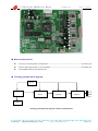
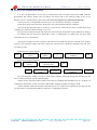
7.1CH Decoder DA32VB User Manual Features Four digital inputs and one analog input, users can extend analog input on your own. 7.1 analog audio input, built-in third-order low-pass filter amplifier circuit. Adopt CS4926 series audio DSP, CS8415 96KHz digital receiver, 96 KHz/24bit ADC and DAC. Support Dolby digital, Dolby pro-logic, DTS, and so on, with many kinds of listening modes and sound field effect playbacks. Built-in analog input mute, when there is no analog signal, the muting process will automatically go on without stop, and there is no need to connect detection circuit outside. Digital and analog ground wires are independent, which lowers the requirement of motherboard PCB LAYOUT and gets better performance. Provide mute control signal output and directly use hardware to mute. STL212 MCU can upgrade directly program online. Users can get new program on Internet when necessary, which provides convenience for debugging and maintenance. 17 universal output ports, it is okay to use built-in CPU to complete whole machine functions. Use I2C slave interface to connect user host, and it is okay to use existing I2C interface without adding additional interface. ¾ I2C interface can be used with another I2C device in parallel. DA32VB is the same as many I2C devices such as 24C01 and so on, and it’s easy for users to do secondary development. I2C communication has TNT interrupt output port, user host can read corresponding data when TNT changes, which reduces the holding time of user host communication. Built-in 60 bytes memory space, its function is the same as 24C01, and there is no need for users to use memory chips such as 24C01, 93C46, and so on any more. Provide software development kit SDK source code, it is convenient for users to do secondary development. Application fields ¾ Digital audio decoder or analog audio decoder. ¾ Multi-channel multimedia sound box with decoding. ¾ Multi-channel AV reception power amplifier. ¾ Computer host peripheral audio decoding device. ¾ Another advanced audio products. Hard & Soft Technology Co., LTD. http://www.HSAV.com Address: second floor, No.199, Longyin 2nd Road, Xixiang, Shenzhen, China TEL: 86-0755-27951479 27950879 FAX: 86-0755-27950879-213 Business contact:[email protected] Technology support:[email protected] 7.1CH Decoder DA32VB User Manual hsavd607.pdf Nov. 2, 2010 Related technical files z 《I2C Device Development User Manual》------------------------------------------------------------hsavd107.pdf z 《ST-991AR5 Upgrade Device User Manual》-------------------------------------------------------hsavd201.pdf z DA32xSDK Software Development Kit Working principle block diagram Power DA32VB Electronic Filter Power volume amplifier amplifier Speaker Display Working principle block diagram without communication © 2002-2010 Hard & Soft Technology Co., LTD. http://www.HSAV.com Page 2 of 8 7.1CH Decoder DA32VB User Manual hsavd607.pdf Nov. 2, 2010 Power DA32VB Electronic Filter Power volume amplifier amplifier Speaker Display User MCU Working principle block diagram with communication Ground wire instructions AGND and GND are not connected inside DA32VB, and need to be connected on the user board. If +5V ground wire and analog ground wire are not connected at the power supply, connection point should be close to the DA32VB pins or connecting at power supply is also acceptable, while the position close to DA32VB is preferable for a better effect. Size and pins instructions CN10 CN9 DA32VB CN8 90mm CN6 80mm CN7 CN5 CN1 CN2 CN3 CN4 103mm 115mm CN1 1 2 3 4 5 6 7 8 Extended interface. 1. GP7 Extended MCU I/O port GP7, standard bi-directional port, built-in pull-up resistor 2. GP8 Extended MCU I/O port GP8, standard bi-directional port, built-in pull-up resistor © 2002-2010 Hard & Soft Technology Co., LTD. http://www.HSAV.com Page 3 of 8 7.1CH Decoder DA32VB User Manual hsavd607.pdf Nov. 2, 2010 3. GP9 Extended MCU I/O port GP9, standard bi-directional port, built-in pull-up resistor 4. GP10 Extended MCU I/O port GP10, standard bi-directional port, built-in pull-up resistor 5. GP11 Extended MCU I/O port GP11, standard bi-directional port, built-in pull-up resistor 6. GP12 Extended MCU I/O port GP12, standard bi-directional port, built-in pull-up resistor 7. GP13 Extended MCU I/O port GP13, standard bi-directional port, built-in pull-up resistor 8. GP14 Extended MCU I/O port GP14, standard bi-directional port, built-in pull-up resistor CN2 1 2 3 4 5 Extended interface. 1. GP2 Extended MCU I/O port GP2, standard bi-directional port, built-in pull-up resistor 2. GP3 Extended MCU I/O port GP3, standard bi-directional port, built-in pull-up resistor 3. GP4 Extended MCU I/O port GP4, standard bi-directional port, built-in pull-up resistor 4. GP5 Extended MCU I/O port GP5, standard bi-directional port, built-in pull-up resistor 5. GP6 Extended MCU I/O port GP6, standard bi-directional port, built-in pull-up resistor CN3 1 2 3 4 5 6 Extended interface. +5V output. 1. +5V 2. GND Digital ground wire input/output. 3. SDA I2C communication SDA port. 4. SCL I2C communication SCL port, it is infrared remote control reception input in common application. 5. GP0 Extended MCU I/O port GP0, standard bi-directional port, built-in pull-up resistor 6. GP1 Extended MCU I/O port GP1, standard bi-directional port, built-in pull-up resistor CN4 1 2 3 Power input interface. 1. -9V 2. AGND 3. +9V -9V input. Analog ground wire input/output. +9V input. CN5, CN6, and CN7: Factory debugging interface, there is no need to pay attention it in general. CN8 1 2 3 4 5 6 7 8 9 10 Audio output interface. © 2002-2010 Hard & Soft Technology Co., LTD. http://www.HSAV.com Page 4 of 8 7.1CH Decoder DA32VB User Manual 1. SBR 2. AGND 3. SBL Surround back left channel signal output. 4. SW Sub woof channel signal output. 5. SR Surround right signal output. 6. SL Surround left signal output. 7. CEN Central channel signal output. 8. FR Front right channel signal output. 9. FL Front left channel signal output. hsavd607.pdf Nov. 2, 2010 Surround back right channel signal output. Analog ground wire input/output. Analog ground wire input/output. 10. AGND CN9 1 2 3 Analog audio input interface. 1. RCH Analog right channel signal input. 2. AGND Analog ground wire input/output. 3. LCH Analog left channel signal input. CN10 1 2 3 4 5 6 7 Digital input interface. 1. RX1 The first digital input. 2. +5V +5V input/output. 3. RX2 The second digital input. 4. GND Digital ground wire input/output. 5. RX3 The third digital input. 6. GND Digital ground wire input/output. 7. RX4 The fourth digital input. Electrical specification Items +5V power supply voltage +5V working current (@ HDMI (DTS)) Digital RX input Analog input effective detection level Signal-to-noise ratio (CIR) Resolution Level output @0dB Analog level input Frequency response(20Hz-20KHz) © 2002-2010 Hard & Soft Technology Co., LTD. Minimum +4.6V 260mA 0.1V(P-P) 0.8 Vrms 90dB - Typical +5V 270mA 0.5V(P-P) 89dB 88dB 1V 2V +/-1dB http://www.HSAV.com Maximum +5.5V 350mA 1.0V(P-P) 95dB 2.2V - Page 5 of 8 7.1CH Decoder DA32VB User Manual Software development instructions hsavd607.pdf Nov. 2, 2010 It is okay for DA32VB to use I2C bus to communicate with user MCU and provide SDK (software development kit) software packet, user can directly use source code in the software packet. If user is not familiar with I2C communication, please refer to I2C device development user manual hsavd107.pdf. If two bytes form 16-bit parameter, the first byte is low bit and the second byte is high bit. If four bytes form 32-bit parameter, the first byte is low bit and the fourth byte is high bit. 0xnn means the described value is uncertain, it may be any values, but its value is within range fixed originally, for instance, instruction length is 2 to 137. B7 means the seventh bit of byte, B6 means the sixth bit of byte, and the rest may be deduced by analogy. I2C address that user host writes DA32VB is 0x32, i.e. 00110010B. I2C address that user host reads DA32VB is 0x33, i.e. 00110011B. The length of register is 8 bits in general, and user host only needs one byte for read and write. Another registers that mark byte length need several bytes for read and write, should do multibyte read and write according to need. DA32VB write register diagram: Device address Register Start (write) address Write data 0 DA32VB read register diagram: Device address Register address waiting Start (write) for being read Start Device address (read) Write data X (when multibyte) End End Read data 0 Read data X (when multibyte) End First use the device address of write to write register address waiting for being read, and then use the device address of read to read corresponding data. Need to receive the ninth ACK bit when write each byte including data and address for I2C, ACK bit is 0 outputted by DA32VB. User host can know if DA32VB is working normally according to ACK. Need to send the ninth ACK bit when read each byte for I2C, ACK bit is 0 outputted by user host, but the last byte needs to send the ninth NAK bit, NAK bit is 1 outputted by user host. © 2002-2010 Hard & Soft Technology Co., LTD. http://www.HSAV.com Page 6 of 8 7.1CH Decoder DA32VB User Manual I C Communication user host instructions set hsavd607.pdf Nov. 2, 2010 2 Address Name 0x00 INTCLR 0x01 INTRD 0x02 INTENA 0x03 POWERON 0x04 DIGITINFO 0x05 CHINFO 0x06 ANASIGNAL 0x07 SFREQFREG 0x0a © 2002-2010 INPUTSEL Description Clear interrupt register (write only) Interrupt number: INT0=1, DA32VB initialization, guarantee that user host and DA32VB connect power synchronously. INT1=1, digital signal input format change, interrupt needs to read “DIGIINFO” register. INT2=1, analogue signal input change interrupt, need to read “ANASIGNAL” register. INT3 to INT7, reserved. Read interrupt register (read only ) Interrupt number is the same as clear interrupt register. Attention: please clear corresponding interrupt number after read, or interrupt will go on without stop. Register writes 1 to clear corresponding interrupt. Interrupt enable register (write only) Set corresponding interrupt enable. DA32VB will generate corresponding interrupt and lower INT pin when status changes. User host needs to detect INT pin and read interrupt value and do corresponding treatment. Interrupt number and read/write interrupt register are corresponding. Allow corresponding interrupt when corresponding bit is 1, and forbid corresponding interrupt when corresponding bit is 0. Digital signal input format indication (read only) B3 is DTS digital signal input. B2 is Dolby digital AC3 signal input. B1 is PCM digital signal input. B0 means that there is no signal input. Dolby digital or DTS input channel information (read only) 0x00 is 1+1, 0x10 is 1/0, 0x20 is 2/0, 0x30 is 3/0, 0x40 is 2/1, 0x50 is 3/1, 0x60 is 2/2, 0x70 is 3/2, 0x90 is 4/2, 0xa0 is 3/2+1, 0xb0 is 4/2, 0xc0 is 5/2, 0xd0 is 4/4, and 0xe0 is 5/3. Analogue signal input level indication (read only) 0 is analogue signal input level, and more than 6mV. 1 is analogue signal input level, and less than 6mV. Enter into mute state and there is no sound output. Sampling frequency (red only) AC-3: 0x00/48K; 0x01/44.1K; 0x02/32K; DTS: 0x0f /Err,0x04/8K,0x05/16K,0x02/32K,0x06/64K,0x07/128K; 0x08/11.025K, 0x09/22.05K, 0x01/44.1K, 0x0a /88.2K, 0x0b /176.4K; 0x0c /12K,0x0d /24K,0x00/48K,0x03/96K,0x0e /192K。 Input port selection (write only) Select analogue signal input when B7 is 1. Select digital input when B7 is 0. B1 to B0 is to select different digital ports: 0x00 means inputting from RX1; 0x01means inputting from RX2; 0x02 means inputting from RX3; 0x03 means inputting from RX4. Hard & Soft Technology Co., LTD. http://www.HSAV.com Page 7 of 8 7.1CH Decoder DA32VB User Manual Address Name hsavd607.pdf Nov. 2, 2010 Description Listening mode selection (write only) Select TEST TONE function When B7 is 1. B3 to B0 is corresponding channel selection, same as sound channel selection codes: 0x00 is left channel, 0x01 is central channel, 0x02 is right channel, 0x03 is right surround channel, 0x04 is left surround channel, 0x05 is sub woof channel, 0x06 is back right channel, 0x07 is back left channel. 0x0b LISTMODE Sending 2.1 sound channel or 5.1 sound channel or 7.1 sound channel exits from TEST TONE. Select standard listening mode when B7 is 0 and B6 is 0. B2 to B0 is to select different effects: 0x00 is automation mode, if input is Dolby digital AC-3 (2.1sound channel), listening mode is AC-3 (2.1sound channel); if input is Dolby digital AC-3 (5.1sound channel), and listening mode is Dolby digital AC-3 (5.1sound channel). 0x01 is stereo, 0x02 is Dolby Pro Logic mode, and 0x03 is 7.1CH. 0x0c SPKCONFIG 0x0d DNYCOMP 0x0e DSPMODE 0x0f VOLCTRL 0x10 to 0x12 0x80 to 0x7d 0xc0 to 0xdd © 2002-2010 DLTIME Speaker setup (write only) Note: big speaker means low, medium, and high bandwidth; small speaker means medium and high bandwidth. It is small speaker when B0 is 0, and it is big speaker when B0 is1. Dolby digital dynamic compression (write only) Only when input digital data rate is Dolby digital AC-3, it is effective. 0x00 is normal playback without compression, the rest are dynamic compression playback. DSP effect setup (write only) B7 is 0 when PCM digital and analogue input, B2 to B0 is to select different DSP effects: 0x00 is HALL, 0x01 is CHURCH, 0x02 is DISCO, 0x03 is THEATER, 0x04 is LIVE, 0x05 is MOVIE, 0x06 is MUSIC, 0x07 is SIMULATE, and 0x08 is exit. Volume setup (write only) 0x00 is minimum volume 0dB, 0x3f is maximum volume 63dB. Channel delay adjustment (write only) 0x10 is CEDLTME, 0x11 is SLDLTME, and 0x12 is SRDLTIME. Central delay writes 0 to 15, it is 0 to15ms in Dolby digital mode. Surround delay writes 0 to 15, it is 0 to 15ms in DTS and Dolby Digital mode, and it is 15ms to 30ms in Dolby Pro Logic mode. Note: it is effective only when listening mode is digital automation or Dolby Pro Logic mode. MEMORYWR FLASH memory space with power-failed memory write MEMORYRD FLASH memory space with power-failed memory read Hard & Soft Technology Co., LTD. http://www.HSAV.com Page 8 of 8