1
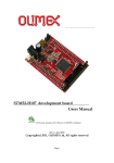
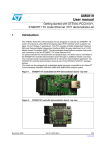
UM0780
User Manual
STM32-MICRIUM
evaluation board for MICRIUM operating system
Introduction
The STM32-MICRIUM evaluation board is a complete development platform for
STMicroelectronic's ARM Cortex™-M3 core-based microcontroller with full-speed USBOTG, Ethernet MAC, two channels of CAN2.0A/B compliant interface, two I2S channels, two
I2C channels, five USARTs with smartcard support, three SPIs, 64 KB internal SRAM and
256 KB Flash, JTAG and SWD debugging support.
The full range of hardware features on the board help you to evaluate all types of peripherals
(USB-OTG FS, Ethernet, CAN, SD/MMC card, USART, temperature sensor, etc.) and
develop your own applications. Extension pin headers and wire wrapping area make it
possible to easily add your own components/interface on the board for a specific application.
Figure 1 shows a picture of the STM32-MICRIUM evaluation board.
Figure 1.
October 2009
STM32-MICRIUM evaluation board
Doc ID 16173 Rev 2
1/27
www.st.com
Contents
STM32-MICRIUM
Contents
1
2
Overview . . . . . . . . . . . . . . . . . . . . . . . . . . . . . . . . . . . . . . . . . . . . . . . . . . 3
1.1
Features . . . . . . . . . . . . . . . . . . . . . . . . . . . . . . . . . . . . . . . . . . . . . . . . . . . 3
1.2
Software example . . . . . . . . . . . . . . . . . . . . . . . . . . . . . . . . . . . . . . . . . . . . 3
1.3
Order code . . . . . . . . . . . . . . . . . . . . . . . . . . . . . . . . . . . . . . . . . . . . . . . . . 3
1.4
Hardware layout . . . . . . . . . . . . . . . . . . . . . . . . . . . . . . . . . . . . . . . . . . . . . 4
Configuration . . . . . . . . . . . . . . . . . . . . . . . . . . . . . . . . . . . . . . . . . . . . . . . 6
2.1
Power supply . . . . . . . . . . . . . . . . . . . . . . . . . . . . . . . . . . . . . . . . . . . . . . . 6
2.2
Boot options . . . . . . . . . . . . . . . . . . . . . . . . . . . . . . . . . . . . . . . . . . . . . . . . 6
2.3
Reset sources . . . . . . . . . . . . . . . . . . . . . . . . . . . . . . . . . . . . . . . . . . . . . . 7
2.4
CAN (controller area network) . . . . . . . . . . . . . . . . . . . . . . . . . . . . . . . . . . 7
2.5
RS-232C . . . . . . . . . . . . . . . . . . . . . . . . . . . . . . . . . . . . . . . . . . . . . . . . . . . 7
2.6
SD/MMC card . . . . . . . . . . . . . . . . . . . . . . . . . . . . . . . . . . . . . . . . . . . . . . . 7
2.7
USB-OTG (USB ON-THE-GO) . . . . . . . . . . . . . . . . . . . . . . . . . . . . . . . . . . 7
2.8
LM75 temperature sensor . . . . . . . . . . . . . . . . . . . . . . . . . . . . . . . . . . . . . 8
2.9
Debug interface . . . . . . . . . . . . . . . . . . . . . . . . . . . . . . . . . . . . . . . . . . . . . 8
2.10
Ethernet . . . . . . . . . . . . . . . . . . . . . . . . . . . . . . . . . . . . . . . . . . . . . . . . . . . 8
2.11
Clock sources . . . . . . . . . . . . . . . . . . . . . . . . . . . . . . . . . . . . . . . . . . . . . . . 9
2.12
Connectors . . . . . . . . . . . . . . . . . . . . . . . . . . . . . . . . . . . . . . . . . . . . . . . . . 9
2.12.1
RS-232C connector (CN7) . . . . . . . . . . . . . . . . . . . . . . . . . . . . . . . . . . . . 9
2.12.2
Power connectors (CN1 and CN9) . . . . . . . . . . . . . . . . . . . . . . . . . . . . . . 9
2.12.3
Extension connector (CN3) . . . . . . . . . . . . . . . . . . . . . . . . . . . . . . . . . . 10
3
I/O assignments . . . . . . . . . . . . . . . . . . . . . . . . . . . . . . . . . . . . . . . . . . . . 11
4
Schematics . . . . . . . . . . . . . . . . . . . . . . . . . . . . . . . . . . . . . . . . . . . . . . . 14
5
Revision history . . . . . . . . . . . . . . . . . . . . . . . . . . . . . . . . . . . . . . . . . . . 26
2/27
Doc ID 16173 Rev 2
STM32-MICRIUM
Overview
1
Overview
1.1
Features
●
1.2
–
256 Kbytes of Flash
–
64 Kbytes of SRAM
●
10/100 Ethernet connector
●
USB-OTG full-speed connector
●
RS-232C connector
●
CAN interface connected to pin headers
●
SD/MMC socket
●
STLM75 temperature sensor
●
3 user LEDs (red, yellow and green)
●
Reset button
●
Free I/O ports connector (pin headers)
●
Prototyping area
●
On-board J-Link SWD for debugging
●
Powered by J-Link USB connector or 5V external power supply on screw terminal
●
RoHS compliant
Software example
●
1.3
72 MHz STM32F107 Cortex™-M3 based microcontroller with:
Example #1 described in the µC/OS-III book is preloaded in the board’s Flash memory
showing the LD1, DL2 & DL3 blinking. For more information on this demonstration
example, please refer to Chapter 3 of the µC/OS-III book .
Order code
●
To order the µC/OS-III book and the STM32-MICRIUM evaluation board, use the order
code STM32CMICOS-EVAL.
Doc ID 16173 Rev 2
3/27
Overview
1.4
STM32-MICRIUM
Hardware layout
The STM32-MICRIUM evaluation board is designed around the STM32F107VCT in a 100pin TQFP package.
Figure 2 illustrates the connection between the STM32F107VCT and peripherals (USBOTG, Ethernet, SD/MMC, RS-232, CAN temperature sensor).
Figure 3 helps you to locate these features on the actual evaluation board.
Figure 2.
4/27
STM32-MICRIUM evaluation board hardware block diagram
Doc ID 16173 Rev 2
STM32-MICRIUM
Figure 3.
Overview
STM32-MICRIUM evaluation board layout
Doc ID 16173 Rev 2
5/27
Configuration
STM32-MICRIUM
2
Configuration
2.1
Power supply
The STM32-MICRIUM evaluation board is powered by a 5V DC power supply. It is
configured via JP5 to use the following power supply sources:
●
5V DC power adapter connected to CN10, the power screw terminal on the board.
●
5V VBUS power (500 mA limitation from CN5), the mini-B USB of embedded J-Link.
Table 1.
STM32-MICRIUM evaluation board power supply jumper
Jumper
Description
Switch
configuration
The board is powered by VBUS of the embedded J-Link input CN5
when JP5 is set as shown on the right: (Default setting).
3 2 1
The board is powered by 5V DC input CN10 when JP5 is set as shown
on the right:
3 2 1
JP5
Note:
2.2
1
The board cannot be powered by VBUS on CN8 when USB-OTG is used as a USB device.
2
The LED LD5 is lit when the STM32CMICOS-EVAL board is powered by the 5V correctly.
3
Three test points TP4 (5V), TP3 (GND), and TP2 (3.3V) are available on the top right of the
board to check power supply.
Boot options
The boot option is configured by setting switch JP3 (BOOT1) and JP4 (BOOT0). The
STM32-MICRIUM evaluation board can boot from:
●
Embedded user Flash.
●
System memory.
●
Embedded SRAM for debugging.
Table 2.
Jumper
JP3 &
JP4
STM32-MICRIUM evaluation board boot options jumpers
Description
Configuration
STM32-MICRIUM evaluation board boots from user Flash when JP4 is
set as shown to the right. JP3 is not relevant in this configuration.
(Default setting).
0 <_> 1
STM32-MICRIUM evaluation board boots from embedded SRAM when
JP3 and JP4 are set as shown to the right.
0 <_> 1
0 <_> 1
STM32-MICRIUM evaluation board boots from system memory when
JP3 and JP4 are set as shown to the right.
6/27
Doc ID 16173 Rev 2
STM32-MICRIUM
2.3
Configuration
Reset sources
The reset signal of the STM32-MICRIUM evaluation board is active low.
The reset source may come from:
2.4
●
Reset button B1 in bottom right of the board.
●
Embedded J-Link.
●
Extension connector CN3 pin 45 (pin header).
CAN (controller area network)
The STM32-MICRIUM evaluation board supports one channel of CAN2.0A/B-compliant
CAN bus communication based on a 3.3V CAN transceiver.
The CAN transceiver (U1) is configured for high-speed mode.
The CAN bus is available on extension connector CN3 pin 28 (CAN_L) and pin 30 (CAN_H).
The CAN interface is connected to CAN1 remapped (PD0, PD1) of the STM32F107VCT.
The CAN terminal (120 ohm), available on the board, can be connected on the bus by the
jumper JP1.
Table 3.
STM32-MICRIUM evaluation board CAN related jumper
Jumper
JP1
2.5
Description
CAN terminal resistor is enabled when JP1 is fitted. Default setting: Not fitted.
RS-232C
The RS-232 communication with hardware flow control is supported by CN7 (a 9-pin D-type
RS-232 connector) and the transceiver U8, which is connected to USART2 remapped on
PD3 to PD6 of STM32F107VCT on STM32-MICRIUM evaluation board.
2.6
SD/MMC card
An SD/MMC card (Secure Digital/Multi-Media Card) connector (CN6) is available on the
board, but the card is not provided by default with the product. The SD/MMC card is
connected to SPI1 of STM32F107VCT (PA5 to PA7 without remap) with chip select on PA8
and card detection on PE6.
2.7
USB-OTG (USB ON-THE-GO)
The STM32-MICRIUM evaluation board supports USB-OTG full-speed communication via a
USB Micro-AB connector (CN8) and USB power switch (U9) connected to VBUS. The
evaluation board cannot be powered by this USB connector.
The green LED LD6 turns on when the power switch (U9) is ON, which corresponds to USBhost mode. In this case, the 5V VBUS is provided by the board to a USB device connected
on CN8. The red LED LD7 turns on when an over-current condition is detected.
Doc ID 16173 Rev 2
7/27
Configuration
2.8
STM32-MICRIUM
LM75 temperature sensor
A 10-bit temperature sensor, STLM75M2E (U7), is connected to the I2C1 bus of the
STM32F107VCT without remap (PB5 to PB7).
2.9
Debug interface
An embedded J-Link (JTAG/SWD development tool from IAR) is available on the STM32MICRIUM evaluation board as the default debugger/programmer interface. The mini-B USB
connector CN5 is used to interface the embedded J-Link (U3) using the IAR Embedded
Workbench for ARM toolchain. The SWD port of the embedded J-Link is directly connected
to the STM32F107VCT debug port and optionally, through solder bridges, to all other JTAG
signals, as detailed in Table 5.
Other debugger/programmer hardware can be supported by the JTAG/SWD signals
available on extension connector CN3. The debug tool used can be selected by the jumper
JP2, as mentioned in Table 4.
Table 4.
STM32-MICRIUM evaluation board J-Link related jumper
Jumper
Description
Open: embedded J-Link is selected as debugger/programmer tool (Default setting).
JP2
Closed: external debugger/programmer tool connected on CN3 is used.
Table 5.
STM32-MICRIUM evaluation board J-TAG solder bridges
Jumper
SB1
Description
Open: J-Link TDO/SWO is not connected to the TDO of the STM32F107VCT.
J-Link supports SWD communication only.
Closed: J-Link TDO/SWO is connected to the TDO of the STM32F107VCT.
J-Link supports JTAG and SWD communication (Default setting).
Open: J-Link TDI is not connected to the TDI of the STM32F107VCT.
J-Link supports SWD communication only.
SB2
Closed: J-Link TDI is connected to the TDI of the STM32F107VCT.
J-Link supports JTAG and SWD communication (Default setting).
Open: J-Link TRST is not connected to the TRST of the STM32F107VCT.
J-Link supports SWD communication only.
SB3
Closed: J-Link TRST is connected to the TRST of the STM32F107VCT.
J-Link supports JTAG and SWD communication (Default setting).
2.10
Ethernet
The STM32-MICRIUM evaluation board supports a 10/100 Ethernet communication
interface with a 'PHY' (DP83848CVV, U2) and integrated RJ45 connector (CN2). MII
interface mode is also supported.
The 25 MHz Ethernet clock is provided by crystal X1 connected to the PHY.
Note:
8/27
Test point TP1 can be used to check the PHY clock frequency.
Doc ID 16173 Rev 2
STM32-MICRIUM
2.11
Configuration
Clock sources
Two clock sources are available on the STM32-MICRIUM evaluation board for the
STM32F107VCT, and also include an embedded RTC:
●
X3, 32.768 KHz crystal for embedded RTC connected to PC14, PC15.
●
X2, 25 MHz crystal for the STM32F107VCT microcontroller.
The PC14 and PC15 are available on extension connector CN3 depending on SB4 and SB5
configuration as mentioned in Table 6.
Table 6.
STM32-MICRIUM evaluation board 32 KHz crystal X3 solder bridges
Jumper
Description
SB4
Open: PC14 is connected to 32 KHz crystal (Default setting).
Closed: P14 is connected to extension connector CN3.
SB5
Open: PC15 is connected to 32 KHz crystal (Default setting).
Closed: P15 is connected to extension connector CN3.
2.12
Connectors
2.12.1
RS-232C connector (CN7)
Figure 4.
STM32CMICOS-EVAL DB-9F RS-232C CN6 with ISP support (front view)
1
2
9
Table 7.
8
4
7
5
6
RS-232C connector CN6 with ISP support
Pin number
2.12.2
3
Description
Pin number
Description
1
NC
6
NC
2
RS232_TXD (PD5)
7
RS232_CTS (PD3)
3
RS232_RXD (PD6)
8
RS232_RTS (PD4)
4
NC
9
NC
5
GND
Power connectors (CN1 and CN9)
The nine pins of connector CN9 on the left side of the wrapping area are connected to the
board's ground.
The eight higher pins of connector CN8 are connected to the 3.3V power. and the lower pin
is connected to the 5V power of the board.
Doc ID 16173 Rev 2
9/27
Configuration
2.12.3
STM32-MICRIUM
Extension connector (CN3)
Table 8.
CN3 pinout
Description
Note:
10/27
Pin name
Pin number of CN3
Pin name
Description
IO port
PA4
1
2
PE3
IO port
IO port
PB0
3
4
PE4
IO port
IO port
PB1
5
6
PB3
IO port or TDO (SB1)
IO port
PB9
7
8
PB4
IO port or TRST (SB3)
IO port
PB14
9
10
PE7
IO port
IO port
PB15
11
12
PE8
IO port
IO port
PC0
13
14
PE9
IO port
IO port
PC4
15
16
PE10
IO port
IO port
PC5
17
18
PE11
IO port
IO port
PC6
19
20
P12
IO port
IO port
PC7
21
22
PE13
IO port
IO port
PC8
23
24
PE14
IO port
IO port
PC9
25
26
PE15
IO port
IO port
PC10
27
28
CAN_L
CAN bus L
IO port
PC11
29
30
CAN_H
CAN bus H
IO port
PC12
31
32
PD6
IO port
IO port
PC13
33
34
PD5
IO port
IO port (SB4)
PC14
35
36
PD4
IO port
IO port (SB5)
PC15
37
38
PD3
IO port
IO port
PD2
39
40
PA15
IO port or TDI (SB2)
IO port
PD7
41
42
PE2
IO port
IO port
PE0
43
44
PA13
IO port or TMS
Board reset
RESET
45
46
PA14
IO port or TCK
(SBx) means that a corresponding solder bridge must be set to enable the signal on the
connector.
Doc ID 16173 Rev 2
STM32-MICRIUM
3
I/O assignments
I/O assignments
Table 9.
I/O assignments
Pin No.
Pin name
1
PE2
IO PORT PE2
2
PE3
IO PORT PE3
3
PE4
IO PORT PE4
4
PE5
MII_INT
5
PE6
SDCard_Detection
6
VBAT
7
PC13-ANTI_TAMP
8
PC14-OSC32_IN
9
STM32-MICRIUM evaluation board processor I/O assignments
IO PORT PC13
OSC32K or IO PORT PC14
PC15-OSC32_OUT OSC32K or IO PORT PC15
10
VSS_5
11
VDD_5
12
OSC_IN
13
OSC_OUT
14
NRST
15
PC0
IO PORT PC0
16
PC1
ETHER_MDC
17
PC2
ETHER_TXD2
18
PC3
ETHER_TX_CLK
19
VSSA
20
VREF
21
VREF+
22
VDDA
23
PA0-WKUP
24
PA1
ETHER_RX_CLK
25
PA2
ETHER_MDIO
26
PA3
ETHER_COL
27
VSS_4
28
VDD_4
29
PA4
IO PORT PA4
30
PA5
SPI_SCK_MMC
31
PA6
SPI_MISO_MMC
32
PA7
SPI_MOSI_MMC
RESET
ETHER_CRS
Doc ID 16173 Rev 2
11/27
I/O assignments
Table 9.
12/27
STM32-MICRIUM
I/O assignments (continued)
Pin No.
Pin name
STM32-MICRIUM evaluation board processor I/O assignments
33
PC4
IO PORT PC4
34
PC5
IO PORT PC5
35
PB0
IO PORT PB0
36
PB1
IO PORT PB1
37
PB2
BOOT1
38
PE7
IO PORT PE7
39
PE8
IO PORT PE8
40
PE9
IO PORT PE9
41
PE10
IO PORT PE10
42
PE11
IO PORT PE11
43
PE12
IO PORT PE12
44
PE13
IO PORT PE13
45
PE14
IO PORT PE14
46
PE15
IO PORT PE15
47
PB10
ETHER_RX_ER
48
PB11
ETHER_TX_EN
49
VSS_1
50
VDD_1
51
PB12
ETHER_TXD0
52
PB13
ETHER_TXD1
53
PB14
IO PORT PB14
54
PB15
IO PORT PB15
55
PD8
ETHER_RX_DV
56
PD9
ETHER_RXD0
57
PD10
ETHER_RXD1
58
PD11
ETHER_RXD2
59
PD12
ETHER_RXD3
60
PD13
LED0
61
PD14
LED1
62
PD15
LED2
63
PC6
IO PORT PC6
64
PC7
IO PORT PC7
65
PC8
IO PORT PC8
66
PC9
IO PORT PC9
67
PA8
SPI_CS_MMC
Doc ID 16173 Rev 2
STM32-MICRIUM
Table 9.
I/O assignments
I/O assignments (continued)
Pin No.
Pin name
STM32-MICRIUM evaluation board processor I/O assignments
68
PA9
VBUS
69
PA10
ID
70
PA11
DM
71
PA12
DP
72
PA13
Debug TMS
73
NC
74
VSS_2
75
VDD_2
76
PA14
Debug TCK
77
PA15
Debug TDI
78
PC10
IO PORT PC10
79
PC11
IO PORT PC11
80
PC12
IO PORT PC12
81
PD0
CAN_RX
82
PD1
CAN_TX
83
PD2
IO PORT PD2
84
PD3
USART_CTS
85
PD4
USART_RTS
86
PD5
USART_TX
87
PD6
USART_RX
88
PD7
IO PORT PD7
89
PB3
Debug TDO
90
PB4
Debug TRST
91
PB5
INT_Temperature
92
PB6
I2C_SCL_Temperature
93
PB7
I2C_SDA_Temperature
94
BOOT0
95
PB8
ETHER_TXD3
96
PB9
IO PORT PB9
97
PE0
IO PORT PE0
98
PE1
USB_PowerSwitchOn
99
VSS_3
100
VDD_3
BOOT0
Doc ID 16173 Rev 2
13/27
Schematics
4
STM32-MICRIUM
Schematics
This section provides the design schematics for the STM32-MICRIUM evaluation board
board key features, to help you implement these features in your applications.
The following schematics are provided:
14/27
●
Figure 5: Block diagram on page 15
●
Figure 6: STM32F107VCT6 on page 16
●
Figure 7: CAN on page 17
●
Figure 8: Ethernet on page 18
●
Figure 9: Extension connector on page 19
●
Figure 10: SD card on page 20
●
Figure 11: Temperature sensor on page 21
●
Figure 12: RS-232 on page 22
●
Figure 13: USB-OTG-FS on page 23
●
Figure 14: J-Link on page 24
●
Figure 15: Power on page 25
Doc ID 16173 Rev 2
Block diagram
1
2
3
CAN_L
CAN_H
CAN1_RX
CAN1_TX
CAN1_RX
CAN1_TX
U_Ethernet
Ethernet.SchDoc
Doc ID 16173 Rev 2
MII_TX_CLK
MII_RX_ER
MII_RX_DV/RMII_CRSDV
MII_RX_CLK/RMII_REF_CLK
MII_COL
MII_CRS
MII_RXD0
MII_RXD1
MII_RXD2
MII_RXD3
MII_INT
MII_TXD3
MII_TXD2
MII_TXD1
MII_TXD0
PHY_RESET#
MII_MDIO
MII_MDC
MII_TX_EN
U_ExtensionConnector
ExtensionConnector.SchDoc
RESET#
CAN_H
CAN_L
U_Power
Power.SchDoc
PA[0..15]
PB[0..15]
PC[0..15]
PD[0..15]
PE[0..15]
LED1
LED2
LED3
SPI1_SCK
SPI1_MOSI
SDCard_CS
SDCard_Detection
SPI1_MISO
SDCard_SCK
SDCard_MOSI
SDCard_CS
SDCard_Detection
SDCard_MISO
MII_TX_CLK
MII_RX_ER
MII_RX_DV/RMII_CRSDV
MII_RX_CLK/RMII_REF_CLKI2C1_SCK
MII_COL
I2C1_SDA
MII_CRS
I2C_SMB
MII_RXD0
MII_RXD1
MII_RXD2
MII_RXD3
USART2_TX
MII_INT
USART2_RTS
MII_TXD3
USART2_CTS
MII_TXD2
USART2_RX
MII_TXD1
MII_TXD0
MII_MDIO
MII_MDC
MII_TX_EN
PA[0..15]
PB[0..15]
PC[0..15]
PD[0..15]
PE[0..15]
LED1
LED2
LED3
4
U_SDCard
SDCard.SchDoc
U_MCU
MCU.SchDoc
U_CAN
CAN.SchDoc
STM32-MICRIUM
Figure 5.
U_TemSensor
TemSensor.SCHDOC
I2C_SLK
I2C_SDA
I2C_SMB
U_USART
USART.SchDoc
USART2_TX
USART2_RTS
USART2_CTS
USART2_RX
U_USB_OTG_FS
USB_OTG_FS.SchDoc
USB_PowerSwitchOn
USB_DM
USB_DP
USB_ID
USB_VBUS
USB_PowerSwitchOn
USB_DM
USB_DP
USB_ID
USB_VBUS
U_J-LINK
J-LINK.SchDoc
TDO/SWO
RESET#
TCK/SWCLK
TMS/SWDIO
TDI
TRST
SB1
SB2
SB3
TDO
nRESET
TCK
TMS
TDI
nTRST
Solder bridges SB1,2 &3 close by default
STMicroelectronics
15/27
Title:
uC/eval-STM32F107
Number:MB834
Rev: B.2(PCB.SCH)
Date: 10/9/2009
Sheet 1 of
11
Schematics
Note1: only default setting of SB1,2 &SB3 was updated to be close from Versioin B.1 to B.2.
STM32F107VCT6
1
2
3
4
PA[0..15]
C27
10pF
3
2
4
1
PB[0..15]
C26
10pF
SPI1_SCK
SPI1_MISO
SPI1_MOSI
SDCard_CS
USB_VBUS
USB_ID
USB_DM
USB_DP
TMS/SWDIO
TCK/SWCLK
TDI
+3V3
JP3
Doc ID 16173 Rev 2
1
2
3
R38
10K
TDO/SWO
TRST
I2C_SMB
I2C1_SCK
I2C1_SDA
MII_TXD3
MII_RX_ER
MII_TX_EN
MII_TXD0
MII_TXD1
PA0
PA1
PA2
PA3
PA4
PA5
PA6
PA7
PA8
PA9
PA10
PA11
PA12
PA13
PA14
PA15
23
24
25
26
29
30
31
32
67
68
69
70
71
72
76
77
PB0
PB1
PB2
PB3
PB4
PB5
PB6
PB7
PB8
PB9
PB10
PB11
PB12
PB13
PB14
PB15
35
36
37
89
90
91
92
93
95
96
47
48
51
52
53
54
PA0-WKUP
PA1
PA2
PA3
PA4
PA5
PA6
PA7
PA8
PA9
PA10
PA11
PA12
PA13
PA14
PA15
PC15-OSC32_OUT
PC14-OSC32_IN
PC13-ANTI_TAMP
PC12
PC11
PC10
PC9
PC8
PC7
PC6
PC5
PC4
PC3
PC2
PC1
PC0
PB0
PB1
PB2
PB3
PB4
PB5
PB6
PB7
PB8
PB9
PB10
PB11
PB12
PB13
PB14
PB15
PD15
PD14
PD13
PD12
PD11
PD10
PD9
PD8
PD7
PD6
PD5
PD4
PD3
PD2
PD1
PD0
X4
25MHz
12
13
14
73
94
C35
20pF
C36
R41
R39
10K
390
B1
2
4
1
1
3
2
20pF
OSC_IN
OSC_OUT
NRST
NC
BOOT0
JP4
PE15
PE14
PE13
PE12
PE11
PE10
PE9
PE8
PE7
PE6
PE5
PE4
PE3
PE2
PE1
PE0
9
8
7
80
79
78
66
65
64
63
34
33
18
17
16
15
PC15
PC14
PC13
PC12
PC11
PC10
PC9
PC8
PC7
PC6
PC5
PC4
PC3
PC2
PC1
PC0
62
61
60
59
58
57
56
55
88
87
86
85
84
83
82
81
PD15
PD14
PD13
PD12
PD11
PD10
PD9
PD8
PD7
PD6
PD5
PD4
PD3
PD2
PD1
PD0
46
45
44
43
42
41
40
39
38
5
4
3
2
1
98
97
PE15
PE14
PE13
PE12
PE11
PE10
PE9
PE8
PE7
PE6
PE5
PE4
PE3
PE2
PE1
PE0
PC[0..15]
X3
MC306-G-06Q-32.768 (manufacturer JFVNY)
U4A
MII_CRS
MII_RX_CLK/RMII_REF_CLK
MII_MDIO
MII_COL
STM32-MICRIUM
Figure 6.
PD[0..15]
PE[0..15]
PA[0..15]
PB[0..15]
PC[0..15]
PD[0..15]
PE[0..15]
MII_TX_CLK
MII_TXD2
MII_MDC
LED3
LED2
LED1
MII_RXD3
MII_RXD2
MII_RXD1
MII_RXD0
MII_RX_DV/RMII_CRSDV
VREF+
VDDA
R40
USART2_RX
USART2_TX
USART2_RTS
USART2_CTS
TP2
C28
VREF
47
103P
U4B
CAN1_TX
CAN1_RX
21
22
50
75
100
28
11
6
L1
+3V3
BEAD
C25
10uF
C29
103P
+3V3
SDCard_Detection
MII_INT
VREF+
VDDA
VDD_1
VDD_2
VDD_3
VDD_4
VDD_5
VBAT
VREFVSSA
VSS_1
VSS_2
VSS_3
VSS_4
VSS_5
20
19
49
74
99
27
10
STM32F107VCT6
+3V3
C30
103P
USB_PowerSwitchOn
C31
103P
C32
103P
C33
103P
C34
103P
STM32F107VCT6
3
+3V3
RESET
R37
+3V3
STMicroelectronics
[N/A]
104P
Title:
16/27
RESET#
uC/eval-STM32F107 MCU
Number:MB834
1
2
3
Rev: B.1(PCB.SCH)
Date: 7/8/2009
4
Sheet 2 of
11
Schematics
C24
CAN
STM32-MICRIUM
Figure 7.
+3V3
C1
Default setting: Open
104P
R1
0
U1
CAN1_TX
CAN1_RX
PD1
PD0
1
2
3
4
D
GND
VCC
R
RS
CANH
CANL
Vref
Doc ID 16173 Rev 2
SN65HVD230
8
7
6
5
JP1
CAN_L
CAN_H
R4
120
Title:
17/27
uC/eval-STM32F107 CAN
Number:MB834
Rev: B.2(PCB.SCH)
Date: 10/9/2009
Schematics
STMicroelectronics
Ethernet
1
2
PA0
PB10
PA3
PD12
PD11
PB8
PC2
PC3
+3V3
C2
104P
+3V3
42
40
MII_MDC
MII_MDIO
PHY_RESET#
31
30
PC1
PA2
+3V3
MII_INT
C10
22pF
C11
22pF
R12
29
7
2K2
33
34
25
X1
25MHz
TP1
25MHz
R15
4.87K
24
37
18
23
+3V3
C48
104P
RS7
75 C51
C49
104P
COL/PHYAD0
CRS/CRS_DV/LED_CFG
MDC
MDIO
11
10
9
RS6
LED_LINK/AN0
LED_SPEED/AN1
LED_ACT/COL/AN_EN
RESET_N
PWR_DOWN/INT
NC
NC
AVDD33
IOVDD33
IOVDD33
X2
X1
25MHz_OUT
AGND
AGND
IOGND
IOGND
DGND
RBIAS
PFBIN2
PFBIN1
PFBOUT
+3V3
C50
104P
1500pF(2KV)
C52
103P
LED2A
LED2K
RX+
RXC
RX-
LED1A
LED1K
+3V3
RD+
RDC
RD-
Shield
Shield
6
7
8
1
2
3
4
5
6
7
8
0
0
33
RXD_0/PHYAD1
RXD_1/PHYAD2
RXD_2/PHYAD3
RXD_3/PHYAD4
RX_ER/MDIX_EN
RX_DV/MII_MODE
RX_CLK
17
16
14
13
12
11
10
9
8
+3V3
28
27
26
21 R13
20 R14
22
48
32
2K2
2K2
2K2
+3V3
R11
600
+3V3
19
15
47
35
36
LD9
Orange[N/A]
R10
600
2
Doc ID 16173 Rev 2
43
44
45
46
41
39
38
TD+
TDRD+
RDNC
NC
NC
NC
NC
1
33
RS4
PD10
PD9
PD8
PA1
TX_CLK
TX_EN
TXD_0
TXD_1
TXD_2
TXD_3/SNI_MODE
2
1
2
3
4
5
6
12
11
U2
RS3
CN2
B563S-8850-U006
Second source may be Q08012317
U5
TS8121C
Second source H1102
1
16
TD+
TX+
2
15
TDC TXC
3
14
TDTX-
10
9
RS2
33
PB11
PB12
PB13
MII_RXD1
MII_RXD0
MII_RX_DV/RMII_CRSDV
MII_RX_CLK/RMII_REF_CLK
C3
104P
RS5
50
R9
1K5
RS1
33
Unused in RMII mode
MII_TX_EN
MII_TXD0
MII_TXD1
4
1
MII_CRS
MII_RX_ER
MII_COL
MII_RXD3
MII_RXD2
MII_TXD3
MII_TXD2
MII_TX_CLK
3
STM32-MICRIUM
Figure 8.
LD8
Green[N/A]
Two LEDs reserved for RJ45 jack without LED
DP83848CVV
+3V3
C4
104P
C5
104P
C6
104P
C12
10uF
+3V3
C7
104P
C8
104P
C9
104P
Title:
uC/eval-STM32F107 Ethernet
18/27
Number:MB834
1
2
3
Rev: B.1(PCB.SCH)
Date: 8/3/2009
4
Sheet 4 of
11
Schematics
STMicroelectronics
Extension connector
LED1
LED2
LED3
PE14
R18
LD1
Green
1
STM32-MICRIUM
Figure 9.
2
600
PD13
PD3
LD2
Orange
R19
1
600
LD3
Red
R20
1
600
2
2
CN3
Doc ID 16173 Rev 2
Close to MCU
PC14
PC15
PA4
PB0
PB1
PB9
PB14
PB15
PC0
PC4
PC5
PC6
PC7
PC8
PC9
PC10
PC11
PC12
PC13
SB4
SB5
PD2
PD7
PE0
RESET#
1
3
5
7
9
11
13
15
17
19
21
23
25
27
29
31
33
35
37
39
41
43
45
2
4
6
8
10
12
14
16
18
20
22
24
26
28
30
32
34
36
38
40
42
44
46
PE3
PE4
PB3
PB4
PE7
PE8
PE9
PE10
PE11
PE12
PE13
PE14
PE15
PD6
PD5
PD4
PD3
PA15
PE2
PA13
PA14
+5V
CN9
CAN_L
CAN_H
1
2
3
4
5
6
7
8
9
10
+3V3
CN1
1
2
3
4
5
6
7
8
9
10
Header 10
Header 10
Wrapping Area 30x70mm
Header 23X2H
PA[0..15]
PB[0..15]
PC[0..15]
PD[0..15]
PE[0..15]
PA[0..15]
PB[0..15]
PC[0..15]
PD[0..15]
PE[0..15]
19/27
Title:
uC/eval-STM32F107 Extension connector
Number:MB834
Rev: B.1(PCB.SCH)
Date: 7/8/2009
Sheet 5 of
11
Schematics
STMicroelectronics
STM32-MICRIUM
Figure 10. SD card
CN6
SDCard_MISO
SDCard_SCK
PA6
PA5
+3V3
Doc ID 16173 Rev 2
SDCard_MOSI
SDCard_CS
PA7
PA8
R46
4K7
8
7
6
5
4
3
2
1
9
nCD
WP
10
11
SDCard_Detection
2508-109-001-200
+3V3
Title:
20/27
uC/eval-STM32F107 SD card
Number:MB834
Rev: B.1(PCB.SCH)
Date: 7/8/2009
Schematics
STMicroelectronics
STM32-MICRIUM
Figure 11. Temperature sensor
+3V3
R47
4K7
R48
4K7
R49
4K7
U7
I2C_SDA
I2C_SLK
I2C_SMB
PB7
PB6
PB5
1
2
3
4
SDA VDD
SCL
A0
OS/INT A1
GND
A2
8
7
6
5
C41
104P
Doc ID 16173 Rev 2
STLM75M2E
Title:
21/27
uC/eval-STM32F107 TemperatureSensor
Number:MB834
Rev: B.1(PCB.SCH)
Date: 7/8/2009
Sheet 7 of
11
Schematics
STMicroelectronics
STM32-MICRIUM
Figure 12. RS-232
+3V3
C42
104P
U8
C43
104P
2
1
C45
104P
Doc ID 16173 Rev 2
USART2_TX
USART2_RX
USART2_RTS
USART2_CTS
3
PD5
11
PD6
12
PD4
10
PD3
9
6
C46
104P
CN7
DB9-female USART2
V+
VCC
C1+
C2-
C1-
C2+
T1in
T1out
R1out
R1in
T2in
T2out
R2out
R2in
V-
GND
TXD
CTS
RXD
RTS
16
5
C44
104P
4
[N/A]
R50
1
6
2
7
3
8
4
9
5
14
13
7
8
15
ST3232ECTR
Title:
22/27
uC/eval-STM32F107 RS232
Number:MB834
Rev: B.1(PCB.SCH)
Date: 7/8/2009
Schematics
STMicroelectronics
STM32-MICRIUM
Figure 13. USB-OTG-FS
+3V3
+3V3
R51
600
USB_PowerSwitchOn
+5V
R55
47K
U9
2
5
4
GND FAULT
IN
OUT
EN
STMPS2141STR
3
1
2
LD6
Green
R54
10K
LD7
Red
CN8
1
2
3
4
5
C47
4.7uF
Doc ID 16173 Rev 2
0
VBUS
DM
DP
ID
GND
Shield
USB_Micro-AB receptacle
2
1
1
R56
300
475900001
USB_VBUS
USB_DM
USB_DP
USB_ID
PA9
PA11
PA12
PA10
R52
R53
22
22
Title:
23/27
uC/eval-STM32F107 USB_OTG_FS
Number:MB834
Rev: B.1(PCB.SCH)
Date: 7/8/2009
Sheet 9 of
Schematics
STMicroelectronics
3
4
CN4
+3V3
+3V3
1
3
5
7
LD4
+3V3
2 R22
220
JTAG selection
LED
OPEN: JTAG active (default)
Close: JTAG disabled,external debugger may be used
red
TDO
nRESET
120
120
120
120
TRSTout
TDIout
TMSout
TCKout
R27
120
TRESout
+3V3
+3V3
TRSTout
TRESout
TRESin
R28
10K
NRST
C15
104P
C16
104P
C17
104P
C20
OSC_IN
22pF
C21
X2
8MHz
+3V3
VDD_3
VSS_3
PB9
PB8
BOOT0
PB7
PB6
PB5
PB4
PB3
PA15
PA14
VBAT
PC13
PC14
PC15
OSC_IN
OSC_OUT
/RST
VSSA
VDDA
PA0
PA1
PA2
+3V3
VDD_2
VSS_2
PA13
PA12
PA11
PA10
PA9
PA8
PB15
PB14
PB13
PB12
36
35
34
33
32
31
30
29
28
27
26
25
DDP
DDM
TDOin
ATTACH
TDOin
TDIout
TCKout
LED
13
14
15
16
17
18
19
20
21
22
23
24
C14
104P
2
C13
104P
1
Doc ID 16173 Rev 2
OSC_IN
OSC_OUT
NRST
1
2
3
4
5
6
7
8
9
10
11
12
PA3
PA4
PA5
PA6
PA7
PB0
PB1
PB2/BOOT1
PB10
PB11
VSS_1
VDD_1
+3V3
TDOin
TRESin
C18
104P
U3
STM32F103C8T6
48
47
46
45
44
43
42
41
40
39
38
37
TRSTin
TDIin
TMSin
TCKin
+3V3
JTAG
JP2
E_JRST
E_JTDO
E_JTDI
E_JTCK
nTRST
TDI
TMS
TCK
R23
R24
R25
R26
4
6
8
E_JTMS
1
E_JTDO
E_JTMS
R21
4K7
E_JRST
E_JTDI
E_JTCK
2
STM32-MICRIUM
Figure 14. J-Link
1
R30
1M
+3V3
OSC_OUT
22pF
R31
R32
R33
22
22
ATTACH
1K5
DDM
DDP
C22
18pF
R29
10K
TCKin
TMSin
TCKout
TDOin
TMSout
TDIin
TRSTin
CN5
USB-5FCMS30NB
U5V
1
VCC
2
D3
D+
4
ID
5
GND
0
SHELL
0
SHELL
C23
18pF
STMicroelectronics
Title:
24/27
uC/eval-STM32F107 J-LINK
Number:MB834
1
2
3
Rev: B.1(PCB.SCH)
Date: 7/8/2009
4
She
Schematics
C19
104P
STM32-MICRIUM
Figure 15. Power
R2
0
U11
ZEN056V130A24LS [N/A]
D1
STPS1L30A E5V
CN10
1
1
2
JP5
3
1
2
282834-2
Screw terminal for power
GND
C40
4.7uF
Vin
1K
1
2
red
U5V
+3V3
Vout
2
C37
10uF
C38
104P
1
Doc ID 16173 Rev 2
3
3
TP5
3V3
U6
LD1117S33TR
+5V
LD5
R42
2
C39
220uF
TP3
Ground
TP4
5V
+5V
Title:
25/27
uC/eval-STM32F107 Power
Number:MB834
Rev: B.1(PCB.SCH)
Date: 7/8/2009
Shee
Schematics
STMicroelectronics
Revision history
5
STM32-MICRIUM
Revision history
Table 10.
26/27
Document revision history
Date
Revision
Changes
14-Sept-2009
1
Initial release.
22-Oct-2009
2
Table 5 default settings changed.
Section 1.2 added, Section 1.3 changed.
Doc ID 16173 Rev 2
STM32-MICRIUM
Please Read Carefully:
Information in this document is provided solely in connection with ST products. STMicroelectronics NV and its subsidiaries (“ST”) reserve the
right to make changes, corrections, modifications or improvements, to this document, and the products and services described herein at any
time, without notice.
All ST products are sold pursuant to ST’s terms and conditions of sale.
Purchasers are solely responsible for the choice, selection and use of the ST products and services described herein, and ST assumes no
liability whatsoever relating to the choice, selection or use of the ST products and services described herein.
No license, express or implied, by estoppel or otherwise, to any intellectual property rights is granted under this document. If any part of this
document refers to any third party products or services it shall not be deemed a license grant by ST for the use of such third party products
or services, or any intellectual property contained therein or considered as a warranty covering the use in any manner whatsoever of such
third party products or services or any intellectual property contained therein.
UNLESS OTHERWISE SET FORTH IN ST’S TERMS AND CONDITIONS OF SALE ST DISCLAIMS ANY EXPRESS OR IMPLIED
WARRANTY WITH RESPECT TO THE USE AND/OR SALE OF ST PRODUCTS INCLUDING WITHOUT LIMITATION IMPLIED
WARRANTIES OF MERCHANTABILITY, FITNESS FOR A PARTICULAR PURPOSE (AND THEIR EQUIVALENTS UNDER THE LAWS
OF ANY JURISDICTION), OR INFRINGEMENT OF ANY PATENT, COPYRIGHT OR OTHER INTELLECTUAL PROPERTY RIGHT.
UNLESS EXPRESSLY APPROVED IN WRITING BY AN AUTHORIZED ST REPRESENTATIVE, ST PRODUCTS ARE NOT
RECOMMENDED, AUTHORIZED OR WARRANTED FOR USE IN MILITARY, AIR CRAFT, SPACE, LIFE SAVING, OR LIFE SUSTAINING
APPLICATIONS, NOR IN PRODUCTS OR SYSTEMS WHERE FAILURE OR MALFUNCTION MAY RESULT IN PERSONAL INJURY,
DEATH, OR SEVERE PROPERTY OR ENVIRONMENTAL DAMAGE. ST PRODUCTS WHICH ARE NOT SPECIFIED AS "AUTOMOTIVE
GRADE" MAY ONLY BE USED IN AUTOMOTIVE APPLICATIONS AT USER’S OWN RISK.
Resale of ST products with provisions different from the statements and/or technical features set forth in this document shall immediately void
any warranty granted by ST for the ST product or service described herein and shall not create or extend in any manner whatsoever, any
liability of ST.
ST and the ST logo are trademarks or registered trademarks of ST in various countries.
Information in this document supersedes and replaces all information previously supplied.
The ST logo is a registered trademark of STMicroelectronics. All other names are the property of their respective owners.
© 2009 STMicroelectronics - All rights reserved
STMicroelectronics group of companies
Australia - Belgium - Brazil - Canada - China - Czech Republic - Finland - France - Germany - Hong Kong - India - Israel - Italy - Japan Malaysia - Malta - Morocco - Philippines - Singapore - Spain - Sweden - Switzerland - United Kingdom - United States of America
www.st.com
27/27
Doc ID 16173 Rev 2