Download Quartus II Introduction Using VHDL Design

Transcript
Quartus II Introduction Using VHDL Design
R
II CAD system. It gives a general overview of a typiThis tutorial presents an introduction to the Quartus
cal CAD flow for designing circuits that are implemented by using FPGA devices, and shows how this flow is
realized in the Quartus II software. The design process is illustrated by giving step-by-step instructions for using
the Quartus II software to implement a very simple circuit in an Altera FPGA device.
The Quartus II system includes full support for all of the popular methods of entering a description of the
desired circuit into a CAD system. This tutorial makes use of the VHDL design entry method, in which the user
specifies the desired circuit in the VHDL hardware description language. Two other versions of this tutorial are
also available; one uses the Verilog hardware description language and the other is based on defining the desired
circuit in the form of a schematic diagram.
The last step in the design process involves configuring the designed circuit in an actual FPGA device. To
show how this is done, it is assumed that the user has access to the Altera DE2 Development and Education board
connected to a computer that has Quartus II software installed. A reader who does not have access to the DE2
board will still find the tutorial useful to learn how the FPGA programming and configuration task is performed.
The screen captures in the tutorial were obtained using the Quartus II version 5.0; if other versions of the
software are used, some of the images may be slightly different.
Contents:
Typical CAD flow
Getting started
Starting a New Project
VHDL Design Entry
Compiling the Design
Pin Assignment
Simulating the Designed Circuit
Programming and Configuring the FPGA Device
Testing the Designed Circuit
1
Computer Aided Design (CAD) software makes it easy to implement a desired logic circuit by using a programmable logic device, such as a field-programmable gate array (FPGA) chip. A typical FPGA CAD flow is
illustrated in Figure 1.
Design Entry
Synthesis
Functional Simulation
No
Design correct?
Yes
Fitting
Timing Analysis and Simulation
No
Timing requirements met?
Yes
Programming and Configuration
Figure 1. Typical CAD flow.
The CAD flow involves the following steps:
• Design Entry – the desired circuit is specified either by means of a schematic diagram, or by using a
hardware description language, such as VHDL or Verilog
• Synthesis – the entered design is synthesized into a circuit that consists of the logic elements (LEs) provided
in the FPGA chip
• Functional Simulation – the synthesized circuit is tested to verify its functional correctness; this simulation
does not take into account any timing issues
2
• Fitting – the CAD Fitter tool determines the placement of the LEs defined in the netlist into the LEs in
an actual FPGA chip; it also chooses routing wires in the chip to make the required connections between
specific LEs
• Timing Analysis – propagation delays along the various paths in the fitted circuit are analyzed to provide
an indication of the expected performance of the circuit
• Timing Simulation – the fitted circuit is tested to verify both its functional correctness and timing
• Programming and Configuration – the designed circuit is implemented in a physical FPGA chip by programming the configuration switches that configure the LEs and establish the required wiring connections
This tutorial introduces the basic features of the Quartus II software. It shows how the software can be used to
design and implement a circuit specified by using the VHDL hardware description language. It makes use of the
graphical user interface to invoke the Quartus II commands. Doing this tutorial, the reader will learn about:
• Creating a project
• Design entry using VHDL code
• Synthesizing a circuit specified in VHDL code
• Fitting a synthesized circuit into an Altera FPGA
• Assigning the circuit inputs and outputs to specific pins on the FPGA
• Simulating the designed circuit
• Programming and configuring the FPGA chip on Altera’s DE2 board
1 Getting Started
Each logic circuit, or subcircuit, being designed with Quartus II software is called a project. The software works
on one project at a time and keeps all information for that project in a single directory (folder) in the file system.
To begin a new logic circuit design, the first step is to create a directory to hold its files. To hold the design files
for this tutorial, we will use a directory introtutorial. The running example for this tutorial is a simple circuit for
two-way light control.
Start the Quartus II software. You should see a display similar to the one in Figure 2. This display consists
of several windows that provide access to all the features of Quartus II software, which the user selects with the
computer mouse. Most of the commands provided by Quartus II software can be accessed by using a set of menus
that are located below the title bar. For example, in Figure 2 clicking the left mouse button on the menu named
File opens the menu shown in Figure 3. Clicking the left mouse button on the entry Exit exits from Quartus II
software. In general, whenever the mouse is used to select something, the left button is used. Hence we will not
normally specify which button to press. In the few cases when it is necessary to use the right mouse button, it will
be specified explicitly.
3
Figure 2. The main Quartus II display.
Figure 3. An example of the File menu.
4
For some commands it is necessary to access two or more menus in sequence. We use the convention Menu1
> Menu2 > Item to indicate that to select the desired command the user should first click the left mouse button
on Menu1, then within this menu click on Menu2, and then within Menu2 click on Item. For example, File >
Exit uses the mouse to exit from the system. Many commands can be invoked by clicking on an icon displayed in
one of the toolbars. To see the command associated with an icon, position the mouse over the icon and a tooltip
will appear that displays the command name.
1.1 Quartus II Online Help
Quartus II software provides comprehensive online documentation that answers many of the questions that may
arise when using the software. The documentation is accessed from the menu in the Help window. To get some
idea of the extent of documentation provided, it is worthwhile for the reader to browse through the Help menu.
For instance, selecting Help > How to Use Help gives an indication of what type of help is provided.
The user can quickly search through the Help topics by selecting Help > Search, which opens a dialog box
into which key words can be entered. Another method, context-sensitive help, is provided for quickly finding
documentation for specific topics. While using most applications, pressing the F1 function key on the keyboard
opens a Help display that shows the commands available for the application.
2 Starting a New Project
To start working on a new design we first have to define a new design project. Quartus II software makes the
designer’s task easy by providing support in the form of a wizard. Create a new project as follows:
1. Select File > New Project Wizard to reach the window in Figure 4, which indicates the capability of this
wizard. You can skip this window in subsequent projects by checking the box Don’t show me this introduction again. Press Next to get the window shown in Figure 5.
Figure 4. Tasks performed by the wizard.
5
Figure 5. Creation of a new project.
2. Set the working directory to be introtutorial; of course, you can use some other directory name of your
choice if you prefer. The project must have a name, which is usually the same as the top-level design entity
that will be included in the project. Choose light as the name for both the project and the top-level entity, as
shown in Figure 5. Press Next. Since we have not yet created the directory introtutorial, Quartus II software
displays the pop-up box in Figure 6 asking if it should create the desired directory. Click Yes, which leads
to the window in Figure 7.
Figure 6. Quartus II software can create a new directory for the project.
6
Figure 7. The wizard can include user-specified design files.
3. The wizard makes it easy to specify which existing files (if any) should be included in the project. Assuming
that we do not have any existing files, click Next, which leads to the window in Figure 8.
Figure 8. Choose the device family and a specific device.
7
4. We have to specify the type of device in which the designed circuit will be implemented. Choose CycloneTM
II as the target device family. We can let Quartus II software select a specific device in the family, or we can
choose the device explicitly. We will take the latter approach. From the list of available devices, choose the
device called EP2C35F672C6 which is the FPGA used on Altera’s DE2 board. Press Next, which opens the
window in Figure 9.
Figure 9. Other EDA tools can be specified.
5. The user can specify any third-party tools that should be used. A commonly used term for CAD software
for electronic circuits is EDA tools, where the acronym stands for Electronic Design Automation. This term
is used in Quartus II messages that refer to third-party tools, which are the tools developed and marketed
by companies other than Altera. Since we will rely solely on Quartus II tools, we will not choose any other
tools. Press Next.
6. A summary of the chosen settings appears in the screen shown in Figure 10. Press Finish, which returns to
the main Quartus II window, but with light specified as the new project, in the display title bar, as indicated
in Figure 11.
8
Figure 10. Summary of the project settings.
Figure 11. The Quartus II display for the created project.
9
3 Design Entry Using VHDL Code
As a design example, we will use the two-way light controller circuit shown in Figure 12. The circuit can be used
to control a single light from either of the two switches, x1 and x2 , where a closed switch corresponds to the logic
value 1. The truth table for the circuit is also given in the figure. Note that this is just the Exclusive-OR function
of the inputs x1 and x2 , but we will specify it using the gates shown.
x1
f
x2
x1 x2
f
0 0
0
0 1
1
1 0
1
1 1
0
Figure 12. The light controller circuit.
The required circuit is described by the VHDL code in Figure 13. Note that the VHDL entity is called light to
match the name given in Figure 5, which was specified when the project was created. This code can be typed into
a file by using any text editor that stores ASCII files, or by using the Quartus II text editing facilities. While the
file can be given any name, it is a common designers’ practice to use the same name as the name of the top-level
VHDL entity. The file name must include the extension vhd, which indicates a VHDL file. So, we will use the
name light.vhd.
LIBRARY ieee ;
USE ieee.std_logic_1164.all ;
ENTITY light IS
PORT ( x1, x2 : IN
STD_LOGIC ;
f
: OUT STD_LOGIC ) ;
END light ;
ARCHITECTURE LogicFunction OF light IS
BEGIN
f <= (x1 AND NOT x2) OR (NOT x1 AND x2);
END LogicFunction ;
Figure 13. VHDL code for the circuit in Figure 12.
3.1 Using the Quartus II Text Editor
This section shows how to use the Quartus II Text Editor. You can skip this section if you prefer to use some other
text editor to create the VHDL source code file, which we will name light.vhd.
Select File > New to get the window in Figure 14, choose VHDL File, and click OK. This opens the Text
Editor window. The first step is to specify a name for the file that will be created. Select File > Save As to open
the pop-up box depicted in Figure 15. In the box labeled Save as type choose VHDL File. In the box labeled
File name type light. Put a checkmark in the box Add file to current project. Click Save, which puts the file
into the directory introtutorial and leads to the Text Editor window shown in Figure 16. Maximize the Text Editor
10
window and enter the VHDL code in Figure 13 into it. Save the file by typing File > Save, or by typing the
shortcut Ctrl-s.
Figure 14. Choose to prepare a VHDL file.
Figure 15. Name the file.
Figure 16. Text Editor window.
11
Most of the commands available in the Text Editor are self-explanatory. Text is entered at the insertion point,
which is indicated by a thin vertical line. The insertion point can be moved either by using the keyboard arrow
keys or by using the mouse. Two features of the Text Editor are especially convenient for typing VHDL code.
First, the editor can display different types of VHDL statements in different colors, which is the default choice.
Second, the editor can automatically indent the text on a new line so that it matches the previous line. Such options
can be controlled by the settings in Tools > Options > Text Editor.
3.1.1 Using VHDL Templates
The syntax of VHDL code is sometimes difficult for a designer to remember. To help with this issue, the Text
Editor provides a collection of VHDL templates. The templates provide examples of various types of VHDL
statements, such as an ENTITY declaration, a CASE statement, and assignment statements. It is worthwhile
to browse through the templates by selecting Edit > Insert Template > VHDL to become familiar with this
resource.
3.2 Adding Design Files to a Project
As we indicated when discussing Figure 7, you can tell Quartus II software which design files it should use as part
of the current project. To see the list of files already included in the light project, select Assignments > Settings,
which leads to the window in Figure 17. As indicated on the left side of the figure, click on the item Files. An
alternative way of making this selection is to choose Project > Add/Remove Files in Project.
Figure 17. Settings window.
If you used the Quartus II Text Editor to create the file and checked the box labeled Add file to current
project, as described in Section 3.1, then the light.vhd file is already a part of the project and will be listed in the
12
window in Figure 17. Otherwise, the file must be added to the project. So, if you did not use the Quartus II Text
Editor, then place a copy of the file light.vhd, which you created using some other text editor, into the directory
introtutorial. To add this file to the project, click on the File name: button in Figure 17 to get the pop-up window
in Figure 18. Select the light.vhd file and click Open. The selected file is now indicated in the Files window of
Figure 17. Click OK to include the light.vhd file in the project. We should mention that in many cases the Quartus
II software is able to automatically find the right files to use for each entity referenced in VHDL code, even if the
file has not been explicitly added to the project. However, for complex projects that involve many files it is a good
design practice to specifically add the needed files to the project, as described above.
Figure 18. Select the file.
4 Compiling the Designed Circuit
The VHDL code in the file light.vhd is processed by several Quartus II tools that analyze the code, synthesize
the circuit, and generate an implementation of it for the target chip. These tools are controlled by the application
program called the Compiler.
Run the Compiler by selecting Processing > Start Compilation, or by clicking on the toolbar icon
that
looks like a purple triangle. As the compilation moves through various stages, its progress is reported in a window
on the left side of the Quartus II display. Successful (or unsuccessful) compilation is indicated in a pop-up box.
Acknowledge it by clicking OK, which leads to the Quartus II display in Figure 19. In the message window, at the
bottom of the figure, various messages are displayed. In case of errors, there will be appropriate messages given.
When the compilation is finished, a compilation report is produced. A window showing this report is opened
automatically, as seen in Figure 19. The window can be resized, maximized, or closed in the normal way, and it
.
can be opened at any time either by selecting Processing > Compilation Report or by clicking on the icon
The report includes a number of sections listed on the left side of its window. Figure 19 displays the Compiler
Flow Summary section, which indicates that only one logic element and three pins are needed to implement this
tiny circuit on the selected FPGA chip. Another section is shown in Figure 20. It is reached by selecting Analysis
& Synthesis > Equations on the left side of the compilation report. Here we see the logic expressions produced
by the Compiler when synthesizing the designed circuit. Observe that f is the output derived as
f = x2 $ x1
where the $ sign is used to represent the Exclusive-OR operation. Obviously, the Compiler recognized that the
logic expression in our design file is equivalent to this expression.
13
Figure 19. Display after a successful compilation.
Figure 20. Compilation report showing the synthesized equations.
4.1 Errors
Quartus II software displays messages produced during compilation in the Messages window. If the VHDL design
file is correct, one of the messages will state that the compilation was successful and that there are no errors.
If the Compiler does not report zero errors, then there is at least one mistake in the VHDL code. In this case
a message corresponding to each error found will be displayed in the Messages window. Double-clicking on an
error message will highlight the offending statement in the VHDL code in the Text Editor window. Similarly, the
Compiler may display some warning messages. Their details can be explored in the same way as in the case of
14
error messages. The user can obtain more information about a specific error or warning message by selecting the
message and pressing the F1 function key.
To see the effect of an error, open the file light.vhd. Remove the semicolon in the statement that defines the
function f , illustrating a typographical error that is easily made. Compile the erroneous design file by clicking on
icon. A pop-up box will ask if the changes made to the light.vhd file should be saved; click Yes. After
the
trying to compile the circuit, Quartus II software will display a pop-up box indicating that the compilation was not
successful. Acknowledge it by clicking OK. The compilation report summary, given in Figure 21, now confirms
the failed result. Expand the Analysis & Synthesis part of the report and then select Messages to have the
messages displayed as shown in Figure 22. Double-click on the first error message. Quartus II software responds
by opening the light.vhd file and highlighting the statement which is affected by the error, as shown in Figure 23.
Correct the error and recompile the design.
Figure 21. Compilation report for the failed design.
Figure 22. Error messages.
Figure 23. Identifying the location of the error.
15
5 Pin Assignment
During the compilation above, the Quartus II Compiler was free to choose any pins on the selected FPGA to serve
as inputs and outputs. However, the DE2 board has hardwired connections between the FPGA pins and the other
components on the board. We will use two toggle switches, labeled SW0 and SW1 , to provide the external inputs,
x1 and x2 , to our example circuit. These switches are connected to the FPGA pins N25 and N26, respectively. We
will connect the output f to the green light-emitting diode labeled LEDG0 , which is hardwired to the FPGA pin
AE22.
Pin assignments are made by using the Assignment Editor. Select Assignments > Pins to reach the window
in Figure 24. Under Category select Pin. Double-click on the entry <<new>> which is highlighted in blue in
the column labeled To. The drop-down menu in Figure 25 will appear. Click on x1 as the first pin to be assigned;
this will enter x1 in the displayed table. Follow this by double-clicking on the box to the right of this new x1
entry, in the column labeled Location. Now, the drop-down menu in Figure 26 appears. Scroll down and select
PIN_N25. Instead of scrolling down the menu to find the desired pin, you can just type the name of the pin (N25)
in the Location box. Use the same procedure to assign input x2 to pin N26 and output f to pin AE22, which results
in the image in Figure 27. To save the assignments made, choose File > Save. You can also simply close the
Assignment Editor window, in which case a pop-up box will ask if you want to save the changes to assignments;
click Yes. Recompile the circuit, so that it will be compiled with the correct pin assignments.
Figure 24. The Assignment Editor window.
Figure 25. The drop-down menu displays the input and output names.
16
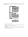
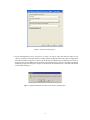
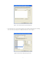
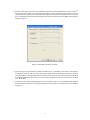
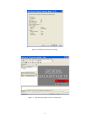
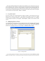
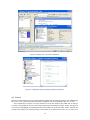
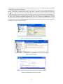
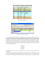
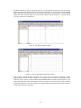
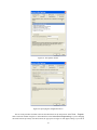
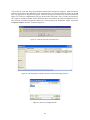
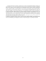
Figure 26. The available pins.
Figure 27. The complete assignment.
The DE2 board has fixed pin assignments. Having finished one design, the user will want to use the same
pin assignment for subsequent designs. Going through the procedure described above becomes tedious if there
are many pins used in the design. A useful Quartus II feature allows the user to both export and import the pin
assignments from a special file format, rather than creating them manually using the Assignment Editor. A simple
file format that can be used for this purpose is the comma separated value (CSV) format, which is a common text
file format that contains comma-delimited values. This file format is often used in conjunction with the Microsoft
Excel spreadsheet program, but the file can also be created by hand using any plain ASCII text editor. The format
for the file for our simple project is
To, Location
x1, PIN_N25
x2, PIN_N26
f, PIN_AE22
By adding lines to the file, any number of pin assignments can be created. Such csv files can be imported into any
design project.
If you created a pin assignment for a particular project, you can export it for use in a different project. To see
how this is done, open again the Assignment Editor to reach the window in Figure 27. Now, select File > Export
which leads to the window in Figure 28. Here, the file light.csv is available for export. Click on Export. If you
17
now look in the directory introtutorial, you will see that the file light.csv has been created.
Figure 28. Exporting the pin assignment.
You can import a pin assignment by choosing Assignments > Import Assignments. This opens the dialogue in Figure 29 to select the file to import. Type the name of the file, including the csv extension and the full
path to the directory that holds the file, in the File Name box and press OK. Of course, you can also browse to find
the desired file.
Figure 29. Importing the pin assignment.
For convenience when using large designs, all relevant pin assignments for the DE2 board are given in the file
called DE2_pin_assignments.csv in the directory DE2_tutorials\design_files, which is included on the CD-ROM
that accompanies the DE2 board and can also be found on Altera’s DE2 web pages. This file uses the names found
in the DE2 User Manual. If we wanted to make the pin assignments for our example circuit by importing this
file, then we would have to use the same names in our VHDL design file; namely, SW(0), SW(1) and LEDG(0)
for x1, x2 and f, respectively. Since these signals are specified in the DE2_pin_assignments.csv file as elements
of arrays SW and LEDG, we must refer to them in the same way in the VHDL design file. For example, in the
DE2_pin_assignments.csv file the 18 toggle switches are called SW[17] to SW[0]; since VHDL uses parentheses
rather than square brackets, these switches are referred to as SW(17) to SW(0). They can also be referred to as an
array SW(17 downto 0).
18
6 Simulating the Designed Circuit
Before implementing the designed circuit in the FPGA chip on the DE2 board, it is prudent to simulate it to
ascertain its correctness. Quartus II software includes a simulation tool that can be used to simulate the behavior
of a designed circuit. Before the circuit can be simulated, it is necessary to create the desired waveforms, called
test vectors, to represent the input signals. It is also necessary to specify which outputs, as well as possible internal
points in the circuit, the designer wishes to observe. The simulator applies the test vectors to a model of the
implemented circuit and determines the expected response. We will use the Quartus II Waveform Editor to draw
the test vectors, as follows:
1. Open the Waveform Editor window by selecting File > New, which gives the window shown in Figure 30.
Click on the Other Files tab to reach the window displayed in Figure 31. Choose Vector Waveform File
and click OK.
Figure 30. Need to prepare a new file.
Figure 31. Choose to prepare a test-vector file.
19
2. The Waveform Editor window is depicted in Figure 32. Save the file under the name light.vwf; note that this
changes the name in the displayed window. Set the desired simulation to run from 0 to 200 ns by selecting
Edit > End Time and entering 200 ns in the dialog box that pops up. Selecting View > Fit in Window
displays the entire simulation range of 0 to 200 ns in the window, as shown in Figure 33. You may wish to
resize the window to its maximum size.
Figure 32. The Waveform Editor window.
Figure 33. The augmented Waveform Editor window.
3. Next, we want to include the input and output nodes of the circuit to be simulated. Click Edit > Insert
Node or Bus to open the window in Figure 34. It is possible to type the name of a signal (pin) into the
Name box, but it is easier to click on the button labeled Node Finder to open the window in Figure 35. The
Node Finder utility has a filter used to indicate what type of nodes are to be found. Since we are interested
in input and output pins, set the filter to Pins: all. Click the List button to find the input and output nodes as
indicated on the left side of the figure.
20
Figure 34. The Insert Node or Bus dialogue.
Figure 35. Selecting nodes to insert into the Waveform Editor.
Click on the x1 signal in the Nodes Found box in Figure 35, and then click the > sign to add it to the Selected
Nodes box on the right side of the figure. Do the same for x2 and f. Click OK to close the Node Finder
window, and then click OK in the window of Figure 34. This leaves a fully displayed Waveform Editor
window, as shown in Figure 36. If you did not select the nodes in the same order as displayed in Figure 36,
it is possible to rearrange them. To move a waveform up or down in the Waveform Editor window, click on
the node name (in the Name column) and release the mouse button. The waveform is now highlighted to
show the selection. Click again on the waveform and drag it up or down in the Waveform Editor.
Figure 36. The nodes needed for simulation.
21
4. We will now specify the logic values to be used for the input signals x1 and x2 during simulation. The logic
values at the output f will be generated automatically by the simulator. To make it easy to draw the desired
waveforms, the Waveform Editor displays (by default) vertical guidelines and provides a drawing feature
that snaps on these lines (which can otherwise be invoked by choosing View > Snap to Grid). Observe also
a solid vertical line, which can be moved by pointing to its top and dragging it horizontally. This reference
line is used in analyzing the timing of a circuit; move it to the time = 0 position. The waveforms can be
drawn using the Selection Tool, which is activated by selecting the icon
Editing Tool, which is activated by the icon
in the toolbar, or the Waveform
.
To simulate the behavior of a large circuit, it is necessary to apply a sufficient number of input valuations and
observe the expected values of the outputs. In a large circuit the number of possible input valuations may
be huge, so in practice we choose a relatively small (but representative) sample of these input valuations.
However, for our tiny circuit we can simulate all four input valuations given in Figure 12. We will use four
50-ns time intervals to apply the four test vectors.
We can generate the desired input waveforms as follows. Click on the waveform name for the x1 node.
Once a waveform is selected, the editing commands in the Waveform Editor can be used to draw the desired
waveforms. Commands are available for setting a selected signal to 0, 1, unknown (X), high impedance (Z),
don’t care (DC), inverting its existing value (INV), or defining a clock waveform. Each command can be
activated by using the Edit > Value command, or via the toolbar for the Waveform Editor. The Edit menu
can also be opened by right-clicking on a waveform name.
Set x1 to 0 in the time interval 0 to 100 ns, which is probably already set by default. Next, set x1 to 1 in the
time interval 100 to 200 ns. Do this by pressing the mouse at the start of the interval and dragging it to its
end, which highlights the selected interval, and choosing the logic value 1 in the toolbar. Make x2 = 1 from
50 to 100 ns and also from 150 to 200 ns, which corresponds to the truth table in Figure 12. This should
produce the image in Figure 37. Observe that the output f is displayed as having an unknown value at this
time, which is indicated by a hashed pattern; its value will be determined during simulation. Save the file.
Figure 37. Setting of test values.
6.1 Performing the Simulation
A designed circuit can be simulated in two ways. The simplest way is to assume that logic elements and interconnection wires in the FPGA are perfect, thus causing no delay in propagation of signals through the circuit. This
is called functional simulation. A more complex alternative is to take all propagation delays into account, which
leads to timing simulation. Typically, functional simulation is used to verify the functional correctness of a circuit
as it is being designed. This takes much less time, because the simulation can be performed simply by using the
logic expressions that define the circuit.
22
6.1.1 Functional Simulation
To perform the functional simulation, select Assignments > Settings to open the Settings window. On the left
side of this window click on Simulator to display the window in Figure 38, choose Functional as the simulation
mode, and click OK. The Quartus II simulator takes the inputs and generates the outputs defined in the light.vwf
file. Before running the functional simulation it is necessary to create the required netlist, which is done by selecting Processing > Generate Functional Simulation Netlist. A simulation run is started by Processing >
Start Simulation, or by using the icon . At the end of the simulation, Quartus II software indicates its successful
completion and displays a Simulation Report illustrated in Figure 39. If your report window does not show the
entire simulation time range, click on the report window to select it and choose View > Fit in Window. Observe
that the output f is as specified in the truth table of Figure 12.
Figure 38. Specifying the simulation mode.
Figure 39. The result of functional simulation.
23
6.1.2 Timing Simulation
Having ascertained that the designed circuit is functionally correct, we should now perform the timing simulation
to see how it will behave when it is actually implemented in the chosen FPGA device. Select Assignments >
Settings > Simulator to get to the window in Figure 38, choose Timing as the simulation mode, and click OK.
Run the simulator, which should produce the waveforms in Figure 40. Observe that there is a delay of about 6
ns in producing a change in the signal f from the time when the input signals, x1 and x2 , change their values.
This delay is due to the propagation delays in the logic element and the wires in the FPGA device. You may also
notice that a momentary change in the value of f , from 1 to 0 and back to 1, occurs at about 106-ns point in the
simulation. This glitch is also due to the propagation delays in the FPGA device, because changes in x1 and x2
may not arrive at exactly the same time at the logic element that generates f .
Figure 40. The result of timing simulation.
7 Programming and Configuring the FPGA Device
The FPGA device must be programmed and configured to implement the designed circuit. The required configuration file is generated by the Quartus II Compiler’s Assembler module. Altera’s DE2 board allows the configuration
to be done in two different ways, known as JTAG and AS modes. The configuration data is transferred from the
host computer (which runs the Quartus II software) to the board by means of a cable that connects a USB port
on the host computer to the leftmost USB connector on the board. To use this connection, it is necessary to have
the USB-Blaster driver installed. If this driver is not already installed, consult the tutorial Getting Started with
Altera’s DE2 Board for information about installing the driver. Before using the board, make sure that the USB
cable is properly connected and turn on the power supply switch on the board.
In the JTAG mode, the configuration data is loaded directly into the FPGA device. The acronym JTAG stands
for Joint Test Action Group. This group defined a simple way for testing digital circuits and loading data into
them, which became an IEEE standard. If the FPGA is configured in this manner, it will retain its configuration
as long as the power remains turned on. The configuration information is lost when the power is turned off. The
second possibility is to use the Active Serial (AS) mode. In this case, a configuration device that includes some
flash memory is used to store the configuration data. Quartus II software places the configuration data into the
configuration device on the DE2 board. Then, this data is loaded into the FPGA upon power-up or reconfiguration.
Thus, the FPGA need not be configured by the Quartus II software if the power is turned off and on. The choice
between the two modes is made by the RUN/PROG switch on the DE2 board. The RUN position selects the JTAG
mode, while the PROG position selects the AS mode.
7.1 JTAG Programming
The programming and configuration task is performed as follows. Flip the RUN/PROG switch into the RUN
position. Select Tools > Programmer to reach the window in Figure 41. Here it is necessary to specify the
programming hardware and the mode that should be used. If not already chosen by default, select JTAG in the
Mode box. Also, if the USB-Blaster is not chosen by default, press the Hardware Setup... button and select the
USB-Blaster in the window that pops up, as shown in Figure 42.
24
Figure 41. The Programmer window.
Observe that the configuration file light.sof is listed in the window in Figure 41. If the file is not already listed,
then click Add File and select it. This is a binary file produced by the Compiler’s Assembler module, which
contains the data needed to configure the FPGA device. The extension .sof stands for SRAM Object File. Note
also that the device selected is EP2C35F672, which is the FPGA device used on the DE2 board. Click on the
Program/Configure check box, as shown in Figure 43.
Figure 42. The Hardware Setup window.
Figure 43. The updated Programmer window.
25
Now, press Start in the window in Figure 43. An LED on the board will light up when the configuration data
has been downloaded successfully. If you see an error reported by Quartus II software indicating that programming
failed, then check to ensure that the board is properly powered on.
7.2 Active Serial Mode Programming
In this case, the configuration data has to be loaded into the configuration device on the DE2 board, which is
identified by the name EPCS16. To specify the required configuration device select Assignments > Device,
which leads to the window in Figure 44. Click on the Device & Pin Options button to reach the window in
Figure 45. Now, click on the Configuration tab to obtain the window in Figure 46. In the Configuration device
box (which may be set to Auto) choose EPCS16 and click OK. Upon returning to the window in Figure 44, click
OK. Recompile the designed circuit.
Figure 44. The Device Settings window.
26
Figure 45. The Options window.
Figure 46. Specifying the configuration device.
The rest of the procedure is similar to the one described above for the JTAG mode. Select Tools > Programmer to reach the window in Figure 41. In the Mode box select Active Serial Programming. If you are changing
the mode from the previously used JTAG mode, the pop-up box in Figure 47 will appear, asking if you want to
27
clear all devices. Click Yes. Now, the Programmer window shown in Figure 48 will appear. Make sure that the
Hardware Setup indicates the USB-Blaster. If the configuration file is not already listed in the window, press Add
File. The pop-up box in Figure 49 will appear. Select the file light.pof in the directory introtutorial and click
Open. As a result, the configuration file light.pof will be listed in the window. This is a binary file produced by
the Compiler’s Assembler module, which contains the data to be loaded into the EPCS16 configuration device.
The extension .pof stands for Programmer Object File. Upon returning to the Programmer window, click on the
Program/Configure check box, as shown in Figure 50.
Figure 47. Clear the previously selected devices.
Figure 48. The Programmer window with Active Serial Programming selected.
Figure 49. Choose the configuration file.
28
Figure 50. The updated Programmer window.
Flip the RUN/PROG switch on the DE2 board to the PROG position. Press Start in the window in Figure
50. An LED on the board will light up when the configuration data has been downloaded successfully. Also, the
Progress box in Figure 50 will indicate when the configuration and programming process is completed, as shown
in Figure 51.
Figure 51. The Programmer window upon completion of programming.
8 Testing the Designed Circuit
Having downloaded the configuration data into the FPGA device, you can now test the implemented circuit. Flip
the RUN/PROG switch to RUN position. Try all four valuations of the input variables x1 and x2 , by setting the
corresponding states of the switches SW1 and SW0 . Verify that the circuit implements the truth table in Figure
12.
If you want to make changes in the designed circuit, first close the Programmer window. Then make the
desired changes in the VHDL design file, compile the circuit, and program the board as explained above.
29
c
Copyright 2005
Altera Corporation. All rights reserved. Altera, The Programmable Solutions Company, the
stylized Altera logo, specific device designations, and all other words and logos that are identified as trademarks
and/or service marks are, unless noted otherwise, the trademarks and service marks of Altera Corporation in
the U.S. and other countries. All other product or service names are the property of their respective holders.
Altera products are protected under numerous U.S. and foreign patents and pending applications, mask work
rights, and copyrights. Altera warrants performance of its semiconductor products to current specifications in
accordance with Altera’s standard warranty, but reserves the right to make changes to any products and services at
any time without notice. Altera assumes no responsibility or liability arising out of the application or use of any
information, product, or service described herein except as expressly agreed to in writing by Altera Corporation.
Altera customers are advised to obtain the latest version of device specifications before relying on any published
information and before placing orders for products or services.
This document is being provided on an “as-is” basis and as an accommodation and therefore all warranties, representations or guarantees of any kind (whether express, implied or statutory) including, without limitation, warranties of merchantability, non-infringement, or fitness for a particular purpose, are specifically disclaimed.
30