1
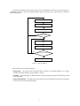
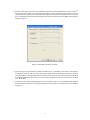
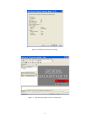
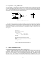
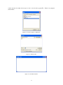
Computer Aided Design (CAD) software makes it easy to implement a desired logic circuit by using a programmable logic device, such as a field-programmable gate array (FPGA) chip. A typical FPGA CAD flow is
illustrated in Figure 1.
Design Entry
Synthesis
Functional Simulation
No
Design correct?
Yes
Fitting
Timing Analysis and Simulation
No
Timing requirements met?
Yes
Programming and Configuration
Figure 1. Typical CAD flow.
The CAD flow involves the following steps:
• Design Entry – the desired circuit is specified either by means of a schematic diagram, or by using a
hardware description language, such as VHDL or Verilog
• Synthesis – the entered design is synthesized into a circuit that consists of the logic elements (LEs) provided
in the FPGA chip
• Functional Simulation – the synthesized circuit is tested to verify its functional correctness; this simulation
does not take into account any timing issues
2