1
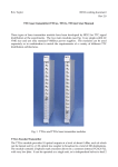
C
TTC machine interface (TTCmi) User Manual
Rev 1.3
B.G. Taylor
Fig. 1 TTCmi minicrate
Introduction
The RD12 TTCmi provides a standard interface between the LHC machine timing which is
broadcast from the Prevessin Control Room (PCR) and the TTC distribution systems of the
individual LHC experiments. The TTCmi consists of a minicrate (see Fig. 1) containing a
number of modules which are configured to suit the requirements of the TTC system of
the LHC experiment. The modules are interconnected by Lemo cables on the front panel.
A few base modules provide for the reception, decoding, conditioning and monitoring of
the optical timing signals which are broadcast to the experiment areas by a high-power
laser transmitter in the PCR. Additional optional modules provide for the optical or
electrical transmission of the TTC signals after the addition of the local Level-1 trigger
accept (L1A) and B-channel commands and data. Other modules provide for the electrical
fanout of the separate 40.08 MHz bunch-crossing and 11.246 kHz LHC orbit clocks to up
to 40 additional trigger partitions at the experiment.
This User Manual is updated and expanded from time to time and comments are
welcome. The latest revision is available from Bruce Taylor or from the RD12 website
http://ttc.web.cern.ch/TTC/intro.html.
Timing signal broadcasting
Fig. 2 is a simplified block diagram of the TTC distribution system which shows where the
TTCmi crates are located in the overall architecture. The 40.08 MHz bunch clock and LHC
and SPS orbit signals generated in the BA3 Faraday Cage are transmitted to the laser
transmitter in the PCR by low-loss coaxial cable links with galvanic isolation. The 43 kHz
SPS orbit signal is only broadcast for special LHC-structured SPS test beam runs. As the
frequency of this signal swings about 29 Hz during acceleration, it is synchronized at the
transmitter to avoid any metastability.
A PLL with low-noise VCXO is used at the transmitter to reduce the jitter of the received
clock to about 7 ps rms and the clock and selected Orbit signal are biphase mark encoded.
The encoded signal modulates a high-power 1310 nm laser diode, the output of which is
2
fanned out by a passive optical tree coupler and broadcast via singlemode fibres to TTCmi
minicrates at each of the experiment and test beam areas.
LHC Clock 40.079 MHz
FARADAY
CAGE
ENCODER
LHC Orbit
11.246 kHz
SPS Orbit
43.375 kHz
SYNC
MODULATOR
PREVESSIN
CONTROL
ROOM
LASER
MONITOR
+16 dBm 1310 nm
1:32 SM TREE COUPLER
-3 dBm
Singlemode fibres
(Max atten 17 dB)
Other LHC experiment areas
Test beam areas
LHC beam instrumentation
Other destinations
LHC
EXPERIMENT
AREA
-20 dBm
TTCmi MINICRATE
LHCrx
TTCcf
Encoder
TTCvi
L1A + Data
LHC Clock + Orbit
LHC Clock + Orbit
to other
TTC partitions
SYSTEM CONTROL
Encoded TTC
L1A
TTCtx
LVL 1
Cal
LVL 1
Muon
0 dBm 1310 nm
GLOBAL TRIGGER
1:32 MM TREE COUPLER
-18 dBm
Multimode fibres
(Max atten 2 dB)
ELECTRONICS CONTROLLER
-20 dBm
I2C
TTCrx
JTAG
Fine and coarse
programmable delays
• 40.079 MHz clock
• Level 1 trigger accept
• Bunch counter reset
• Bunch crossing number
• Event counter reset
• Event number
• Broadcast commands
• Subaddress
• Addressed parameters
Fig. 2 Overall block diagram of TTC distribution
Principle of operation
A block diagram of the TTCmi is shown in Fig. 3. After level adjustment, optoelectronic
conversion and amplification, the composite encoded signal received from the PCR
transmitter is decoded by a TTCrx ASIC in the LHCrx which extracts the 40.08 MHz bunch
clock and 11.246 kHz (LHC) or 43.375 kHz (SPS) orbit clock.
3
Singlemode
fibre from
PCR Tx
DC-coupled
ECL O/Ps
(Max 2 x 40)
88.924 µs
LHC
ORBIT
Max
attenuation
17 dB
0-3563 x 25 ns
40.08 MHz
CLK
GLOBAL ORBIT
PHASE
LEVEL
1 µs
-20 dBm
LHC
ORBIT
1310 nm
PIN +
PREAMP
READY
TTCrx
RST
Optional
TTCvi
40.08 MHz
CLK
SW REG
BM
ENCODER
80 ps
Tx
Optional
encoded
optical
O/Ps
80.16 MHz
OSC
÷2
Optional
encoded
electrical
O/Ps
Ø
VCXO
160.32 MHz
÷4
7 ps
LHC
ORBIT
PLL
CD
MONITOR Rx
40.08 MHz BC Clock
(Square wave)
40.08 MHz
CLK
Fig. 3 TTCmi block diagram
To compensate for the phase differences in the orbit signal received at different points
around the LHC ring, the LHCrx incorporates a digital phase adjustment which allows the
phase of the signal to be set throughout the 88.924 µs period in 3564 steps of the bunchcrossing interval of about 25 ns. The orbit output is a DC-coupled ECL negative-going 1µs
pulse train, as this is the signal for which the TTCvi orbit input circuit was designed. The
orbit signal is fanned-out as required by TTCcf modules in the TTCmi.
4
As the raw 40.08 MHz bunch clock output of the TTCrx has too large a jitter to be used for
the master reference for an LHC experiment, this signal is used as the reference phase for
a 160.32 MHz VCXO/PLL in the TTCmi. The VCXO has a very low internal noise, which
allows it to be used with a narrow loop bandwidth so that the output jitter is determined
by the sub-harmonic feedthrough from the fundamental oscillator rather than the noise on
the reference signal.
The VCXO output signal drives the local biphase mark encoder and its frequency is
divided by 4 before it is fanned out by TTCcf modules to the external TTCex and TTCvi
modules in the TTC system. The jitter of the clock signal at the output of the TTCcf
modules relative to the clock at the PCR transmitter is typically about 10 ps rms.
Configuration
The actual configuration of modules supplied in a TTCmi crate can vary somewhat and
the illustration in Fig. 1 is only representative. From left to right the following modules
may be present:
First 5 slots:
Optional TTCcf (TTC Clocks Fanout) modules
Optional TTCmx Laser or LED Optical Tx modules
Optional -2v Regulator and Fanout modules
TDM Biphase Mark Encoder module
160.32 MHz VCXO-PLL module
-2v Regulator and Test Switch or Fanout module
Local Clock Generator module
LHCrx module
Triple Power Supply, ±15v and +5v
Main Power Supply, -5.2v
Power supply filter module
Signal standards
All electrical inputs and outputs at front panel Lemo connectors have 10E ECL signal
swings. Balanced signals which have no DC component (e.g., the Encoder Sync signal, the
Biphase Mark Encoder output and the Monitor output of the LHCrx) are AC coupled and
may be viewed directly by an oscilloscope with a 50 Ω termination to ground. Signals
which may not be DC balanced (e.g., Test Switch outputs, A and B Channel data inputs to
the Encoder, Orbit clock outputs and all TTCcf inputs and outputs) are standard ECL
levels and the terminations for these are 50 Ω to -2v or Thevenin equivalent.
The standard ECL signal sockets are identified by a round blue label, while the ACcoupled signal sockets have no such label. The outputs are well buffered from internal
timing circuits sensitive to skew and jitter by ganged internally-terminated drivers.
Each TTCcf module (see Fig. 4) comprises two independent 1x9 sections, one of which
would normally be used for the bunch clock and the other for the orbit clock fanout. In
some experiments there is a need in the control room to supply more equipment with the
bunch clock than the orbit clock. Both sections of each TTCcf have DC-coupled ECL
inputs and outputs and they can be used interchangeably for either signal to match such a
5
requirement. The modules can be configured in a tree structure to reduce the cabling
required to supply many destinations from a central point.
AC coupling can be used at the bunch clock destinations. For the orbit clock, DC coupling
should be maintained from the LHCrx through to each TTCvi since the signal is not
balanced and has a low repetition rate. The TTCvi orbit input itself has AC coupling with
a DC offset bias. The following TTCvi circuitry triggers from only the leading edge of the
negative-going 1 µs input pulse.
Fig. 4 TTCcf modules
You can plug around compatible signals quite freely. For example, if you want to send a
square test waveform just plug the 40.08 MHz or 80.16 MHz clock output directly into a
TTCcf, TTCmx or Optical Tx module. Or if you want to lock the VCXO to a reference
received over an optical link, just plug the LHCrx Monitor O/P directly into the VCXOPLL REF I/P, etc. For simplicity only the standard interconnections most commonly used
for operation of the TTCmi are described in detail in the following sections of this manual.
Optical input from PCR
The optical timing signal from the transmitter in the PCR is delivered by singlemode fibre
to a standard patchboard which is located in the vicinity of the rack chosen for the TTCmi.
For redundancy, the same signal is provided via two separate fibres from the PCR. The
active optical connector of the patchboard is linked to the main Input socket of the LHCrx
by a special singlemode FC/PC – ST/PC patchcord which is supplied with the equipment.
When the TTCmi is installed, the optical signal level is set to the optimum value by a
singlemode ST optical attenuator inserted at the Input socket. The attenuator should not
be removed!
6
Reset/Ready
The green Ready LED on the LHCrx front panel (see Fig. 5) indicates when the TTCrx
ASIC in the module is phase locked to the optical signal received from the PCR. Although
the PCR transmitter is normally left running continuously, interruptions for special tests
may occur outside the periods when physics runs are foreseen.
Fig. 5 LHCrx
While a manual Reset switch is provided below the Ready LED, all the LHCrx modules
have now been retrofitted with the most recent version of the TTCrx ASIC which
incorporates a phaselock watchdog circuit. This ensures that the TTCrx PLL will
automatically relock when the transmitter signal is restored after a break.. A reset is also
automatically generated when the TTCmi is initially powered on.
Orbit signal
The ECL Orbit output signal from the LHCrx is simply connected directly to one of the
Inputs of a TTCcf module, the outputs from which are linked to the Orbit Inputs of the
TTCvi modules for each of the trigger partitions. If more than 9 outputs of the Orbit signal
are required, the Input sockets of one or more additional TTCcf modules should be
connected to Outputs of the first module to implement the required fanout. Alternatively
the modules can be daisy-chained as shown in Fig. 4.
Each of the PCR transmitters can be switched to broadcast either the LHC (11.246 kHz) or
the SPS (43.375 kHz) Orbit signal.
7
Orbit phase adjustment
Three rotary Orbit phase adjustment switches in the LHCrx module allow the phase of the
master Orbit signal to be brought within the range of the coarse delay adjustments (16
steps of the bunch period of about 25 ns) in the TTCrx ASICs of the local TTC system of
the experiment.
Fig. 6 Orbit phase switches
The phase of the signal can be varied throughout the full LHC period to compensate for
any experiment location around the ring. The least significant switch SW1 (see Fig. 6)
adds delay in steps of the bunch period of about 25 ns. Each step of SW2 corresponds to a
full rotation of SW1 (400 ns) and each step of the most significant switch SW3 to a full
rotation of SW2 (6.4 µs).
The LHC Orbit signal broadcast from the PCR has an arbitrary but invariable phase
relative to the structure of the circulating beams. In fact the timing of the filling of the
LHC and the phasing of the extractor gap will be determined by this signal. Once the
Orbit phase switches have been set for the experiment location they should not require
adjustment again.
40.08 MHz clock signal
The connections for the 40.08 MHz clock distribution are only slightly more complicated.
One of the 40.08 MHz outputs of the LHCrx is connected to the I/P socket of the Clock
Generator module. The Clock Generator module has three 40.08 MHz outputs but in the
TTCmi application only one of these should be used and linked to the REF I/P of the
VCXO-PLL module. When the clock selector switch is in the EXT position the clock
received from the PCR is used, whereas in the INT position the local 40.08 MHz oscillator
is used. After switching from EXT to INT it takes several seconds for the local oscillator to
start up. Note that, since the Clock Generator outputs when the selector switch is in the
8
EXT position are the raw output of the TTCrx, these outputs must not be used as a trigger
when making jitter measurements.
The 160.32 MHz O/P of the VCXO-PLL module is linked to the adjacent 160.32 MHz I/P
of the Encoder module and one of the two SYNC O/Ps of the Encoder module should be
linked back to the MON I/P of the VCXO-PLL module to close the loop. Do not omit this
essential feedback connection! With these connections the Encoder clock (divided down
to 40.08 MHz) is locked in phase with the reference signal from the PCR or the local Clock
Generator.
This 40.08 MHz clock signal must be connected from the other SYNC O/P of the Encoder
to the Input of a TTCcf module, the outputs from which are linked to the Clock Inputs of
the TTCex encoder/transmitter modules for each of the trigger partitions. For the first
trigger partition using the Encoder in the TTCmi itself, an output should be connected to
the Clock Input of the associated TTCvi module. If more than 9 outputs of the Clock
signal are required, the Input sockets of one or more additional TTCcf modules should be
connected to Outputs of the first module to implement the required fanout. Alternatively,
if the small cumulative jitter can be tolerated, the modules can be daisy-chained as shown
in Fig. 4.
Encoder input signals
The A and B Data I/Ps of the Encoder module should be connected to the A/ecl and B/ecl
CHANNEL OUT sockets of the associated TTCvi module using the same cable lengths for
each. See later sections for the adjustment of the timing of these signals by setting the BC
Delay switch on the front panel of the TTCvi and for the phasing of the external trigger
source.
The 80.16 MHz O/P or the additional 40.08 MHz O/P of the VCXO-PLL module may be
used to clock a PRBS generator or other synchronous test equipment for clock jitter or BER
measurement. Note that since these clock signals are derived from a separate divider from
that in the Encoder module, the 40.08 MHz O/P of the VCXO-PLL does not necessarily
have the same phase as the SYNC O/P of the Encoder module. Only the SYNC O/P
should be used to drive the TTCcf modules.
For tests with a PRBS generator the ECL O/Ps of the test generator should be connected to
the A and B Data I/Ps of the Encoder module. If a single channel test generator is used it
may be clocked at 80.16 MHz to obtain different data on the A and B channels. (The A
Channel data are latched during the first half of the 25 ns bunch crossing interval and the
B Channel data during the second half).
Test switches
The two O/Ps on the -2v Regulator module are simply ECL logic levels which are
controlled by the two switches on its front panel. The upper switch controls the upper
O/P and the lower switch the lower O/P. Switch up selects logic 1 and switch down
logic 0. These O/Ps can, for example, be linked to the A and B Channel data I/Ps of the
Encoder for test purposes. With both switches at 0 the output of the Encoder should be a
40.08 MHz square wave and with both switches at 1 it should be an 80.16 MHz square
wave. Transmission of the Idle sequence with no trigger accepts and no data being
transmitted corresponds to A Channel switch 0 and B Channel switch 1.
9
TTCvi BC Delay adjustment
The TTCvi associated with the Encoder in the TTCmi receives the 40.08 MHz clock from a
TTCcf module in the TTCmi. The TTCvi internally delays this clock by an adjustable time
in order that the phases of the internally-generated A and B channel signals which it
delivers to the Encoder can be set correctly, taking into account the propagation delays of
the interconnecting coaxial cables.
Fig. 7 BC Delay switch
This clock delay is adjusted by the BC Delay rotary switch at the top of the front panel of
the TTCvi (see Fig. 7), which should be set when the TTCvi is initially installed or if the
lengths of any of the cables connecting it to the Encoder are changed.
25 ns
SYNC OUTPUT
∆t
DATA INPUTS
Fig. 8 BC Delay timing adjustment
To set the BC Delay switch, insert Lemo Y adapters at the SYNC O/P and A and B Data
I/P sockets of the Encoder to allow these signals to be monitored with a scope probe.
Program a VME loop so that the TTCvi generates internal triggers at a high rate and adjust
the switch such that the signal transitions on the Data channels occur 4.2 ns after the
10
falling edge of the SYNC signal, as shown in Fig. 8 (∆t = 4.2 ns). The BC Delay switch
allows the timing to be adjusted in steps of 2 ns and the switch position which gives the
timing nearest the optimum setting should be chosen.
External trigger source timing
In order to minimise the Level-1 trigger latency, the TTCvi does not resynchronize the
L1A<0> input which it receives from the Central Trigger Processor or other external
trigger source. Hence the timing of the Encoder A data input signal routed through the
TTCvi from its L1A<0> input is not affected by the TTCvi BC Delay switch and it must be
adjusted at the external trigger source itself to obtain the correct phasing at the A data
input socket of the Encoder.
25 ns
SYNC OUTPUT
∆s
∆h
A DATA INPUT
Fig. 9 Encoder A channel timing for external trigger
To set the timing for an external trigger source connected to the TTCvi LIA<0> input,
insert Lemo Y adapters at the SYNC output and the A data input socket of the Encoder to
allow these signals to be monitored with a scope probe. Select L1A<0> trigger input in
TTCvi CSR1. The duration and phasing of the external trigger signal source should be
such that the Encoder A data input signal is valid for a minimum setup time of ∆s = 6.3 ns
before the rising edge of the SYNC O/P and a minimum hold time of ∆h = 2.2 ns after it.
(See Fig. 9). Outside this interval the A data input signal is a "Don't care".
It should be noted that the L1A<0> input of the TTCvi is AC-coupled, which could result
in a level shift at high data rates. The maximum L1A signal duration should therefore be
chosen to avoid significant DC offset at the highest trigger rate.
VCXO phase
There is a VCXO phase adjustment accessible from the front panel. Please don't touch it as
it is set up on a test bench and, if you have a problem, twiddling this adjustment is sure to
get you in deeper trouble. Because the phase is set up in a standard way, you will not
have to make any adjustments if you exchange the VCXO-PLL module for another.
11
Driving an internal TTCmx or a LED Optical Tx
Either TTCmx laser transmitter modules or LED Optical Tx modules may optionally be
plugged into the TTCmi minicrate.
When operating with an internal TTCmx module (see Fig. 10), one of the ENC O/Ps of the
Encoder module should be connected to the I/P socket of the TTCmx.
Fig. 10 TTCmx laser transmitter
Each of the 4 optical outputs of a TTCmx can be fanned out by a 1:32 TTCoc optical tree
coupler (see Fig. 11) so that the module can broadcast to a total of 128 destinations. For
larger trigger partitions TTCmx modules can be daisy chained by linking the O/P socket
of each module to the I/P socket of the next.
Fig. 11 TTCoc 1:32 optical tree coupler
When operating with one or two LED Optical Tx modules, their I/Ps should be linked to
the ENC O/Ps of the Encoder module. When operating with three or four Tx modules, an
additional -2v Regulator and Fanout module is added and its I/P linked to one of the
12
Encoder O/Ps. The other Encoder O/P drives the first Tx module and the three O/Ps of
the Fanout module drive the other three Tx modules.
Unlike the optical outputs of the TTCmx laser transmitter module, the outputs of the LED
Optical Tx module cannot be fanned out - each of the outputs is at the correct level to
drive just one receiver. To avoid noise generation any unused LED Tx modules should be
removed from the crate.
Driving a TTCtx
When operating with an external TTCtx laser transmitter module, which is housed in a
VMEbus crate, one of the ENC O/Ps of the Encoder module should be connected to the
I/P socket of the TTCtx (see Fig. 12).
Fig. 12 TTCtx laser transmitter
Each of the 14 optical outputs of a TTCtx can be fanned out by a TTCoc 1:32 optical tree
coupler so that the module can broadcast to a total of 448 destinations. For larger trigger
13
partitions TTCtx modules can be daisy chained by linking the I/O socket of each module
to the I/P socket of the next.
Driving a TTCex
The Encoder module included in the TTCmi crate itself provides only for the first trigger
partition. For driving additional partitions the 40.08 MHz clock outputs of the TTCcf
modules should be connected to external TTCex encoder/transmitter modules (see
Fig. 13), which are housed in a VMEbus crate or crates.
Fig. 13 TTCex laser encoder/transmitter
The TTCvi modules for each partition receive their clock signals from the TTCex modules
with which they are associated.
Each of the 10 optical outputs of a TTCex can be fanned out by a TTCoc 1:32 optical tree
coupler so that the module can broadcast to a total of 320 destinations.
14
The TTCex module contains 2 encoders driven by a common internal VCXO/PLL with
very low jitter. It can be operated as a single unit, or in independent halves to feed 2 small
partitions of up to 160 destinations each. For larger trigger partitions of more than 320
destinations the ENC1 O/P of the TTCex module should be connected to the I/P socket of
an expansion TTCtx module.
Additional details of all the laser transmitter modules are given in the RD12 working
document "TTC laser transmitter (TTCex, TTCtx, TTCmx) User Manual", which is
available from the TTC website or from Bruce Taylor.
Optical outputs
ST/PC optical connectors such as 3M/Dorran Type FO-6105 should be used to connect
optical fibres to the TTCmx, TTCtx, TTCex or LED Optical Tx outputs. Index-matching gel
should not be used. Note that a tiny dust particle can completely block the optical output
and the dust caps supplied should be kept on unused optical outputs and inputs. Don't
touch the ends of the ferrules with fingers or allow them to trail on the floor. Impregnated
optical instrument tissues such as "Kodak lens cleaning paper" are recommended for
cleaning.
When the ST Tx and Rx receptacles are new the connector ferrules can be quite stiff. In
case of low optical signal level check that they are fully home since the bayonet caps can
be locked before they are completely inserted.
Optical fibre
All the optical transmitter outputs are intended for operation with 50/125 µm gradedindex multimode fibre with a numerical aperture of 0.2 and a minimum bandwidth of
400 MHz.km at 1300 nm. Fibre attenuation at this wavelength should be less than
3 dB/km.
For safety reasons, only fibre with a Low-Smoke Zero-Halogen (LSZH) sheath should be
used, although if you employ hot melt connectors you may find the low melting point of
such material an inconvenience. Optical fibre purchase requisitions at CERN are
controlled to enforce the LSZH requirement and if you bring PVC-sheathed fibre to CERN
it may not be permitted at the LHC.
Ready-connectorised multimode optical patchcords for interconnecting the RD12 TTC
distribution modules have been standardised in CERN stores in a range of overall lengths
as follows:
04.67.00.005.9
04.67.00.015.7
04.67.00.050.4
04.67.00.150.1
04.67.00.500.9
(L = 0.5 m)
(L = 1.5 m)
(L = 5 m)
(L = 15 m)
(L = 50 m)
CERN stores do not supply separate optical fibre, connectors or accessories like adapters,
couplings, splices and attenuators. 3M/Dorran Type FO-6112 couplings suitable for
concatenating the patchcords are available from Bruce Taylor.
15
Monitor Rx
The upper part of the LHCrx contains a Monitor Rx which may be used to check the
incoming optical signal from the PCR or the outgoing signals from any of the Optical Txs.
The Monitor Rx accepts singlemode or multimode fibre inputs. CD is a carrier detect
indicator. The ECL-swing output of the Monitor Rx is AC coupled and may be connected
directly to an oscilloscope or other test instrument with a 50 Ω termination to ground.
External clock
Normally the system runs from either the LHC bunch clock received by the LHCrx,
selected when the switch on the Clock Generator module is in the EXT position, or its
internal 40.08 MHz clock, selected with the switch in the INT position. However, another
external clock of frequency 40.08 MHz ± 50 ppm can be supplied to the lowest I/P socket
on the Clock Generator module for test purposes if desired.
Note that ± 50 ppm is only ± 2 kHz so you cannot use a 40.00 MHz source. An ECL swing
signal is required and the internal termination is 50 Ω to ground. To ensure an accurate
50/50 mark/space ratio the clock must be derived by subdivision of an 80.16 MHz source
and if no degradation is to occur relative to the internal clock it should have an rms jitter
of less than 6 ps and ground offsets between the external source and the mini-crate should
be avoided.
Jumpers
Some of the modules such as the Clock Generator, LHCrx, -2v Regulator, VCXO-PLL and
Fanout have internal jumpers. These are to allow the same modules to be used in different
equipment, and different versions of the TTCrx ASIC to be used in the LHCrx, and their
settings should not be changed.
Cooling
The modules contain ECLinPS ICs and power regulators and also temperature-sensitive
analogue circuits, optoelectronic components and two quartz oscillators. The power
connection from the crate backplane to the ventilation unit under the modules should
never be disconnected and some clearance should be provided for air intake below the
fans. (e.g., if the crate is operated on a table instead of in a rack it should be supported a
little above the table surface).
Replacement filters for the ventilation unit are available. As there are different filters for
the different types of ventilation unit which have been fitted, be sure to quote the Crate ID
No. when requesting them.
Lemo cables
During the mid-1990s CERN received a consignment of yellow-labelled black Lemo cables
of all lengths which had defective crimping, causing intermittent contacts, and many of
these were distributed before the defect was discovered. The Lemo cables supplied with
the mini-crates have been tested and should be trouble-free but defective ones may be
encountered if they are changed.
After the manufacturing problem was rectified, the black Lemo cables were fabricated
with green labels instead of yellow ones. Current production is yellow-labelled cables
16
with a brown sheath. In case any yellow-labelled black cables are suspect, change them
for green-labelled black ones or yellow-labelled brown ones.
Upgrading
TTC transmitter minicrates previously supplied for development work can be upgraded to
a TTCmi by some backwiring changes and the addition of LHCrx and TTCcf modules.
Safety
The optical output from TTCex and TTCtx modules and some optional optical
transmitters in a TTCmi crate is invisible infra-red energy at a wavelength of about
1300 nm and power level of up to +3 dBm. Never bring the eye close to the open end of an
optical connector when the equipment is powered on.
There are 220v connections to power supplies at the back of the crate. Remove the mains
cable from the power input module before any intervention.
Identification
The Crate ID No. (e.g., M18) in a circular white label above the right chassis handle allows
the records of the status of a TTCmi crate to be checked. It can be helpful to quote it with
any query.
Online spares
Since the TTCmi of each LHC experiment must be functional for the experiment to take
data, arrangements have to be made for rapid replacement in the event of a breakdown.
Since central support staff are not available outside normal working hours, the LECC has
decided (meeting of 6 July 2001) that each experiment will be equipped with a second
TTCmi as an "online spare".
The second TTCmi will be located adjacent to the main one, ready to be switched in
should a problem develop. For additional redundancy, and to aid diagnostic work, the
spare TTCmi will receive the timing signals from the PCR transmitter continuously over a
separate fibre. With the two TTCmi crates mounted one above the other, the signals can
be routed between modules in the two crates by changing coax patchcords. For example,
the 40.08 MHz clock and Orbit signals from one TTCmi can be connected to drive all the
TTCcf modules of the other without moving the modules themselves or disturbing their
multiple output cables.
Support contact
In case of any problems with the PCR transmitter or your TTCmi contact:
Bruce Taylor
CERN/EP
[email protected]
Tel: (+4122) 767 3420
TTC website: http://ttc.web.cern.ch/TTC/intro.html