1
External Interfaces
6
External Interfaces
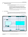
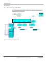
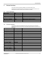
This section shows the interfaces available on the Customer DUT FPGA.
The direction of the signals is shown from the point of view of the DUT FPGA, so an O
signal goes from the DUT FPGA to the CPU FPGA (for example).
6.1
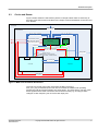
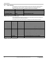
Clocks and Resets
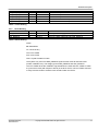
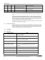
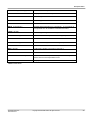
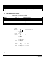
Signal
USER_RESETn
HPE_RESETn
DUT_CLK1
DUT_CLK4
DUT_CLK10
DUT_CLK13
DUT_CLK100M
DUT_PLL_B1_CLKOUT3
DUT_PLL_R2_CLKOUT0
DUT_PLL_T1_CLKOUT3
Direction [Width]
input
input
input
input
input
input
input
output
output
output
Note
AHB system clock input
Video Pixel Clock input
Peripheral reference clock input
AACI bit clock input (x2)
Reference 100MHz input
25MHz reference clock from FPGA PLL
AACI 24.576MHz bit clock x2 from FPGA PLL
Video Pixel Clock from FPGA PLL
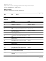
Table 15: Clocks and Resets
6.2
Processor Interface
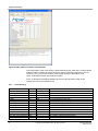
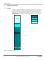
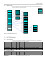
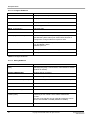
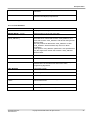
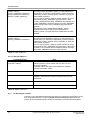
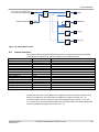
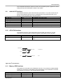
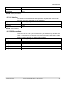
This interface contains the 32bit AHB-Lite bus from the processor to the peripherals
together with interrupts to the processor and sideband signals between the processor and
peripherals.
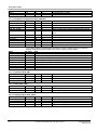
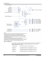
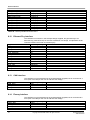
FPGA Signal
FPGA_IC[31:0]
FPGA_IC[32]
FPGA_IC[35:33]
FPGA_IC[36]
FPGA_IC[40:37]
FPGA_IC[43:41]
FPGA_IC[45:44]
FPGA_IC[46]
FPGA_IC[78:47]
FPGA_IC[110:79]
FPGA_IC[111]
FPGA_IC[112]
FPGA_IC[113]
FPGA_IC[125:114]
L14_DUTOUT_DN[11:0]
L14_DUTOUT_DN[12]
L14_CPUOUT_DN[0]
L14_CPUOUT_DN[1]
L14_CPUOUT_DN[2]
L14_CPUOUT_DN[3]
L14_CPUOUT_DN[4]
L14_CPUOUT_DN[5]
L14_CPUOUT_DN[6]
L14_CPUOUT_DN[12:7]
L14_CPUOUT_DP[9:0]
L14_CPUOUT_CLK
Function
HWDATA[31:0]
HWRITE
HBURST[2:0]
HMASTLOCK
HPROT[3:0]
HSIZE[2:0]
HTRANS[1:0]
HSEL
HADDR[31:0]
HRDATA[31:0]
HRESP
HREADY
HRESETn
INT[11:0]
INT[23:12]
NMI
SLEEPING
SLEEPDEEP
HALTED
LOCKUP
TXEV
RXEV
WDOGRES
N/C
N/C
N/C
Note
Not used, driven high by the CPU FPGA
Interrupt signals to processor
Interrupt signals to processor
Non maskable interrupt to processor
Table 16: Processor interface
Application Note 227
ARM DAI0227A
Copyright © 2009 ARM Limited. All rights reserved.
37