1
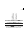
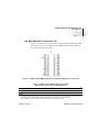
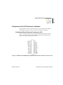
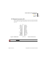
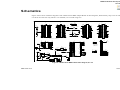
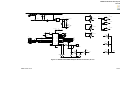
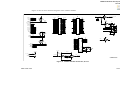
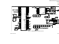
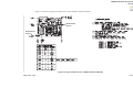
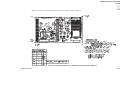
eZ80F91 Modular Development Kit
User Manual
8
Table 1. eZ80Acclaim! MDS Adapter Board Peripheral Bus Connector J1
Identification1,2 (Continued)
Pin
Symbol
Signal Direction
Active Level
eZ80F91 Signal
29
CS3
Output
Low
Yes
30
CS0
Output
Low
Yes
33
F91_WE
Input
Low
No
34
CS2
Output
Low
Yes
35
D3
Bidirectional
n/a
Yes
36
RTC_VDD
Input
n/a
Yes
39
D7
Bidirectional
n/a
Yes
40
HALT_SLP
Output
Low
Yes
41
A13
Bidirectional
n/a
Yes
42
WR
Output
Low
Yes
43
A12
Bidirectional
n/a
Yes
44
A11
Bidirectional
n/a
Yes
45
A14
Bidirectional
n/a
Yes
46
A9
Bidirectional
n/a
Yes
49
A16
Bidirectional
n/a
Yes
50
A5
Bidirectional
n/a
Yes
51
A15
Bidirectional
n/a
Yes
52
A4
Bidirectional
n/a
Yes
Note
Jumper on
board
Notes:
1. To simplify the interface description, Power and Ground nets are omitted from this table. The entire interface
is represented in the eZ80Acclaim! MDS Adapter Board schematics; see Figures 8 and 9.
2. External capacitive loads on RD, WR, IORQ, MREQ, D0–D7 and A0–A23 should be below 10 pF to satisfy the
timing requirements for the eZ80 CPU. All unused inputs should be pulled to either VDD or GND, depending on
their inactive levels, to reduce power consumption and to reduce noise sensitivity. To prevent EMI, the EZ80CLK
output can be deactivated via software in the eZ80F91 MCU’s Peripheral Power-Down Register.
UM017010-0112
eZ80F91 Module Interface