1
eZ80Acclaim!® Microcontrollers
eZ80F91 Development
Kit
User Manual
UM014220-0508
Copyright ©2008 by Zilog®, Inc. All rights reserved.
www.zilog.com
eZ80F91 Development Kit
User Manual
ii
Revision History
Each instance in Revision History reflects a change to this document from
its previous revision. For more details, refer to the corresponding pages
and appropriate links in the table below.
Date
UM014220-0508
Revision
Level
Description
Page No
May
2008
20
Updated Figure 24 and Figure 25.
Updated Zilog logo, Zilog text, Disclaimer
section.
63 and
64
June
2007
19
Introduction, eZ80F91 Module, ZDS II.
2, 1, 55
9 VDC power supply replaced with 6 VDC
power supply on later builds. Windows
Vista added.
April
2007
18
No changes to content.
April
2007
17
Introduction and Troubleshooting. Updated 55, 56
user interfaces for ZDS II and how to
download code.
June
2006
16
Introduction. Added section covering
board hardware revision history.
2
Revision History
eZ80F91 Development Kit
User Manual
iii
Safeguards
The following precautions must be observed when working with the
devices described in this document.
Caution: Always use a grounding strap to prevent damage resulting from
electrostatic discharge (ESD).
UM014220-0508
Safeguards
eZ80F91 Development Kit
User Manual
iv
Table of Contents
Introduction . . . . . . . . . . . . . . . . . . . . . . . . . . . . . . . . . . . . . . . . . . . . .
Kit Features . . . . . . . . . . . . . . . . . . . . . . . . . . . . . . . . . . . . . . . . . . .
Hardware Specifications . . . . . . . . . . . . . . . . . . . . . . . . . . . . . . .
eZ80F91 Development Board Revision History . . . . . . . . . . . . .
eZ80F91 Development Kit Overview . . . . . . . . . . . . . . . . . . . . . . . .
1
1
2
2
3
eZ80 Development Kit. . . . . . . . . . . . . . . . . . . . . . . . . . . . . . . . . . . . . 7
Functional Description . . . . . . . . . . . . . . . . . . . . . . . . . . . . . . . . . . . 7
Physical Dimensions . . . . . . . . . . . . . . . . . . . . . . . . . . . . . . . . . 9
Operational Description . . . . . . . . . . . . . . . . . . . . . . . . . . . . . . . . . 10
eZ80F91 Module Interface . . . . . . . . . . . . . . . . . . . . . . . . . . . . 10
Application Module Interface . . . . . . . . . . . . . . . . . . . . . . . . . . 19
I/O Functionality . . . . . . . . . . . . . . . . . . . . . . . . . . . . . . . . . . . . 22
Embedded Modem Socket Interface . . . . . . . . . . . . . . . . . . . . 25
eZ80Acclaim!® Development Kit Memory . . . . . . . . . . . . . . . . 28
LEDs . . . . . . . . . . . . . . . . . . . . . . . . . . . . . . . . . . . . . . . . . . . . . 31
Push Buttons . . . . . . . . . . . . . . . . . . . . . . . . . . . . . . . . . . . . . . 33
Jumpers . . . . . . . . . . . . . . . . . . . . . . . . . . . . . . . . . . . . . . . . . . 34
Connectors . . . . . . . . . . . . . . . . . . . . . . . . . . . . . . . . . . . . . . . . 40
Console . . . . . . . . . . . . . . . . . . . . . . . . . . . . . . . . . . . . . . . . . . 41
Modem . . . . . . . . . . . . . . . . . . . . . . . . . . . . . . . . . . . . . . . . . . . 41
I2C Devices . . . . . . . . . . . . . . . . . . . . . . . . . . . . . . . . . . . . . . . . . . 41
eZ80F91 Module . . . . . . . . . . . . . . . . . . . . . . . . . . . . . . . . . . . . . . . .
Functional Description . . . . . . . . . . . . . . . . . . . . . . . . . . . . . . . . . .
Fast Buffer . . . . . . . . . . . . . . . . . . . . . . . . . . . . . . . . . . . . . . . .
Physical Dimensions . . . . . . . . . . . . . . . . . . . . . . . . . . . . . . . .
Operational Description . . . . . . . . . . . . . . . . . . . . . . . . . . . . . . . . .
eZ80F91 Module Memory . . . . . . . . . . . . . . . . . . . . . . . . . . . .
Reset Generator . . . . . . . . . . . . . . . . . . . . . . . . . . . . . . . . . . . .
UM014220-0508
42
42
42
44
47
48
48
Table of Contents
eZ80F91 Development Kit
User Manual
v
IrDA Transceiver . . . . . . . . . . . . . . . . . . . . . . . . . . . . . . . . . . .
Flash Loader Utility . . . . . . . . . . . . . . . . . . . . . . . . . . . . . . . . . . . .
Mounting the Module . . . . . . . . . . . . . . . . . . . . . . . . . . . . . . . . . . .
Changing the Power Supply Plug . . . . . . . . . . . . . . . . . . . . . . . . .
49
51
51
52
ZPAK II . . . . . . . . . . . . . . . . . . . . . . . . . . . . . . . . . . . . . . . . . . . . . . . .
ZDI Target Interface Module . . . . . . . . . . . . . . . . . . . . . . . . . . . . .
JTAG . . . . . . . . . . . . . . . . . . . . . . . . . . . . . . . . . . . . . . . . . . . . . . .
Application Modules . . . . . . . . . . . . . . . . . . . . . . . . . . . . . . . . . . . .
54
54
54
54
ZDS II . . . . . . . . . . . . . . . . . . . . . . . . . . . . . . . . . . . . . . . . . . . . . . . . . 55
Troubleshooting . . . . . . . . . . . . . . . . . . . . . . . . . . . . . . . . . . . . . . . .
Overview . . . . . . . . . . . . . . . . . . . . . . . . . . . . . . . . . . . . . . . . . . . .
Cannot Download Code . . . . . . . . . . . . . . . . . . . . . . . . . . . . . . . . .
IrDA Port Not Working . . . . . . . . . . . . . . . . . . . . . . . . . . . . . . . . . .
56
56
56
56
Schematics . . . . . . . . . . . . . . . . . . . . . . . . . . . . . . . . . . . . . . . . . . . . 57
eZ80F91 Development Platform . . . . . . . . . . . . . . . . . . . . . . . 57
eZ80F91 Module . . . . . . . . . . . . . . . . . . . . . . . . . . . . . . . . . . . 62
Appendix A—General Array Logic Equations . . . . . . . . . . . . . . . . 65
U10 Address Decoder . . . . . . . . . . . . . . . . . . . . . . . . . . . . . . . 65
U15 Address Decoder . . . . . . . . . . . . . . . . . . . . . . . . . . . . . . . 68
Customer Support. . . . . . . . . . . . . . . . . . . . . . . . . . . . . . . . . . . . . . . 72
UM014220-0508
Table of Contents
eZ80F91 Development Kit
User Manual
1
Introduction
Zilog’s eZ80F91 Development Kit provides a general-purpose platform
for evaluating the capabilities and operation of eZ80F91 microcontroller.
The eZ80F91 is a member of eZ80Acclaim!® product family, which
offers on-chip Flash capability. The eZ80F91 Development Kit features
two primary boards: the eZ80Acclaim! Development Kit and the
eZ80F91 Module. This arrangement provides a full development platform
when using both the boards. It can also provide a smaller-sized reference
platform with the eZ80F91 Module as a stand-alone development tool.
Kit Features
The key features of the eZ80F91 Development Kit include:
•
UM014220-0508
eZ80Acclaim! Development Kit:
– Up to 2 MB fast SRAM (12 ns access time; 1 MB factoryinstalled, with 512 KB on module, 512 KB on platform)
– Embedded modem socket with a U.S. telephone line interface
– I2C EEPROM
– I2C configuration register
– GPIO, logic circuit, and memory headers
– Supported by Zilog Developer Studio II and the eZ80® C-Compiler
– LEDs, including a 7x 5 LED matrix
– Platform configuration jumpers
– Two RS-232 connectors—console, modem
– RS-485 connector with cable assembly
– Zilog Debug Interface (ZDI)
– JTAG Debug Interface
Introduction
eZ80F91 Development Kit
User Manual
2
–
–
9 VDC power connector
Telephone jack
•
eZ80F91 Module:
– eZ80F91 device operating at 50 MHz, with 256 KB of internal
Flash memory and 8 KB of internal SRAM memory
– 512 KB of off-chip SRAM memory
– 1 MB of off-chip Flash memory (footprint)
– On-chip Ethernet Media Access Controller (EMAC)
– Ethernet port
– IrDA port
– Real-Time Clock with battery backup
– Two headers compatible with the eZ80Acclaim!® Development
Kit
•
•
ZPAK II Debug Tool
eZ80Acclaim! Software and Documentation CD-ROM
Hardware Specifications
Table 2 lists the specifications of the eZ80Acclaim! Development Kit.
Table 2. eZ80Acclaim!® Development Kit Hardware Specifications
Operating Temperature
20 ºC±5 ºC
Operating Voltage
9 VDC (on earlier builds supplied with a 9 VDC power supply)
6 VDC (on later builds supplied with 6 VDC power supply)
eZ80F91 Development Board Revision History
99C0858-001 Rev C or later
10/20/03—Updated layout and added reset fix.
UM014220-0508
Introduction
eZ80F91 Development Kit
User Manual
3
05/30/06—The following components are not populated on the board:
– U11: Triac, SCR Phone Line D0-214
– U26 and U27: IC RS485, XCVR, Low PWR, 8-SOIC
– C3 and C4: CAP 1000 pF Ceramic Disc 1 KV
– D1 and D3: Diode LED Amber 0805 SMT
– T1: Inductor Ferrite Bead, 2x15 Turns
– J1: Conn HDR/Pin 1x32 2 mm socket
– J5: Conn HDR/Pin 1x2 2 mm socket
– J9: Conn HDR/Pin 1x9 2 mm socket
– P4: Conn RJ14 Jack 6-Pos 4-CKT
– P5: Conn 9-CKT Cir rt-angl PC Mount
eZ80F91 Development Kit Overview
The purpose of the eZ80F91 Development Kit is to provide a set of tools
for evaluating the features of the eZ80F91 microcontroller and to be able
to develop a new application before building application hardware.
The eZ80Acclaim!® Development Kit is designed to accept a number of
application-specific modules and eZ80Acclaim!-based add-on modules,
including the eZ80F91 Module featured in this kit.
The eZ80Acclaim! Development Kit, together with its plugged-in
eZ80F91 Module, can operate in stand-alone mode with Flash memory, or
interface via the ZPAK II Debug Tool or USB Smart Cable
(ZUSBSC0100ZACG) to a host PC running Zilog Developer Studio II
Integrated Development Environment (ZDS II IDE) software.
The address bus, data bus, and all eZ80F91 Module control signals are
buffered on the eZ80Acclaim! Development Kit to provide sufficient
drive capability.
A block diagram of the eZ80Acclaim! Development Kit and the eZ80F91
Module is shown in Figure 1.
UM014220-0508
Introduction
eZ80F91 Development Kit
User Manual
4
GPIO
eZ80F91
Address Bus
Data Bus
PHY
GPIO
¤
eZ80
Module
Interface
Address Bus
Data Bus
SRAM
(512 KB
up to 2 MB)
RS232-0
(Console)
RS232-1
(Modem)
Flash
(1 MB)
RS485_0/1
Connect
SRAM
(512 KB)
LED
(7x5 matrix)
Embedded
Modem
GPIO
and
Address
Decoder
IrDA
Transceiver
External
Battery
I2C
EEPROM
I2C
Register
eZ80F91
Module
Application Module Headers
Figure 1. eZ80Acclaim! ® Development Kit Block Diagram with eZ80F91 Module
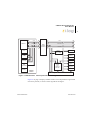
Figure 2 on page 5 displays eZ80Acclaim!® Development Kit segmented
into its key blocks, as shown in the legend for the figure.
UM014220-0508
Introduction
eZ80F91 Development Kit
User Manual
5
C
A
B
D
E
Note: The above is an example only and might have a different configuration. See Table 2.
Key to blocks A–E:
A.
B.
C.
D.
E.
Power and serial communications
eZ80F91 Module interface
JTAG and ZDI debug interfaces
Application module interfaces
GPIO and LED with Address Decoder
Figure 2. The eZ80Acclaim!® Development Kit
UM014220-0508
Introduction
eZ80F91 Development Kit
User Manual
6
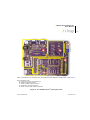
Figure 3 displays the eZ80F91 Module segmented into its key blocks, as
shown in the legend for the figure.
A
B
D
C
A
Note: Key to blocks A–C.
A.
B.
C.
D.
eZ80F91 Module interfaces.
eZ80F91 CPU.
10/100 BaseT Ethernet Interface
IrDA transceiver.
Figure 3. The eZ80F91 Module
The structures of the eZ80Acclaim!® Development Kit and the eZ80F91
Module are displayed in the Schematics on page 57.
UM014220-0508
Introduction
eZ80F91 Development Kit
User Manual
7
eZ80 Development Kit
This section describes the eZ80Acclaim!® Development Kit hardware, its
key components and its interfaces, including programming information
such as memory maps and register definitions.
Functional Description
The eZ80Acclaim! Development Kit consists of seven major hardware
blocks. These blocks are listed below (see Figure 4 on page 8).
UM014220-0508
•
•
eZ80F91 Module interface (2 female headers)
•
•
•
•
•
•
Application Module interface (2 male headers)
Power supply for the eZ80Acclaim! Development Kit, the eZ80F91
Module, and application modules
GPIO and LED matrix
Two RS-232 serial communications ports
Two RS-485 ports
Embedded modem interface
I2C devices
eZ80 Development Kit
eZ80F91 Development Kit
User Manual
8
GPIO
¤
eZ80
Module
Interface
Address Bus
Data Bus
SRAM
(512 KB
up to 2 MB)
RS232-0
(Console)
RS232-1
(Modem)
RS485_0/1
Connect
LED
(7x5 matrix)
Embedded
Modem
GPIO
and
Address
Decoder
I2C
EEPROM
I2C
Register
Application Module Headers
Figure 4. Basic eZ80Acclaim!® Development Kit Block Diagram
UM014220-0508
eZ80 Development Kit
eZ80F91 Development Kit
User Manual
9
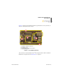
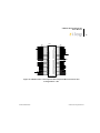
Physical Dimensions
The dimensions of the eZ80Acclaim!® Development Kit PCB is 177.8
mm x 182.9 mm. The overall height is 38.1 mm. See Figure 5.
175.3 mm
43.2 mm
114.3 mm
96.5 mm
55.9 mm
157.5 mm
167.6 mm
5.1 mm
165.1 mm
5.1 mm
Figure 5. Physical Dimensions of the eZ80Acclaim!® Development Kit
UM014220-0508
eZ80 Development Kit
eZ80F91 Development Kit
User Manual
10
Operational Description
The eZ80Acclaim!® Development Kit can accept any eZ80®-core-based
modules, provided that the module interfaces correctly to the
eZ80Acclaim! Development Kit. The purpose of the eZ80Acclaim!
Development Kit is to provide you a tool to evaluate the features of the
eZ80F91 device, and to develop an application without building additional hardware.
eZ80F91 Module Interface
The eZ80Acclaim! Development Kit provides an easy interface for connecting each of the development modules in the eZ80Acclaim! family,
including the eZ80F91 Module. The eZ80F91 Module interface consists
of two 50-pin receptacles, JP1 and JP2; a third receptacle, JP3, enables
the programming of internal on-chip Flash memory.
Almost all these receptacles’ signals are connected directly to the CPU.
Five input signals, in particular, offer you options by disabling certain
functions of the eZ80F91 Module.
These five input signals1 are:
•
•
•
•
•
Enable Flash (EN_Flash)
Flash Write Enable (FlashWE)
Disable IrDA (DIS_IrDA)
F91_WE
RTC_V DD
1. These input signals are only used if external Flash memory is present on the eZ80F91 Module. As shipped
from the factory, external Flash is not installed.
UM014220-0508
eZ80 Development Kit
eZ80F91 Development Kit
User Manual
11
The description of these five signals are provided below.
Enable Flash—When active Low, the EN_Flash input signal enables the
Flash chip on the eZ80F91 Module.
Flash Write Enable—When active Low, the FlashWE input signal
enables write operations on the Flash boot block of the eZ80F91 Module.
Disable IrDA—When the DIS_IrDA input signal is pulled Low, the IrDA
transceiver, located on the eZ80F91 Module, is disabled. As a result,
UART0 can be used with the RS-232 or the RS-485 interfaces on the
eZ80Acclaim!® Development Kit.
F91_WE—When the F91_WE signal is active Low, internal Flash on the
eZ80F91 Module is enabled for writing. This signal is inverted from the
WP signal of on the eZ80F91 Module.
RTC_VDD—RTC_VDD is a test point for the Real Time Clock power sup-
ply.
Peripheral Bus Connector
Figure 6 displays the pin layout of the Peripheral Bus Connector in the
50-pin header, located at position JP1 on the eZ80Acclaim! Development
Kit. Table 3 on page 13 lists the pins and their functions.
UM014220-0508
eZ80 Development Kit
eZ80F91 Development Kit
User Manual
12
JP1
A6
A10
GND_EXT
A8
A13
A15
A18
A19
A2
A11
A4
A5
DIS_ETH
A21
A22
CS0
CS2
D1
D3
D5
D7
MREQ
GND_EXT
WR
BUSACK
1
3
5
7
9
11
13
15
17
19
21
23
25
27
29
31
33
35
37
39
41
43
45
47
49
2
4
6
8
10
12
14
16
18
20
22
24
26
28
30
32
34
36
38
40
42
44
46
48
50
A0
A3
V3.3_EXT
A7
A9
A14
A1 6
GND_EXT
A1
A12
A20
A17
DIS_FLASH
V3.3_EXT
A23
CS1
D0
D2
D4
GND_EXT
D6
IOREQ
RD
INSTRD
BUSREQ
HEADER 25X2
IDC50
Figure 6. eZ80Acclaim!® Development Kit Peripheral Bus Connector Pin
Configuration—JP1
UM014220-0508
eZ80 Development Kit
eZ80F91 Development Kit
User Manual
13
Table 3. eZ80Acclaim! ® Development Kit Peripheral Bus Connector Identification—
JP11,3
Symbol
1
A6
Bidirectional
Yes
2
A0
Bidirectional
Yes
3
A10
Bidirectional
Yes
4
A3
Bidirectional
Yes
5
GND
6
VDD
7
A8
Bidirectional
Yes
8
A7
Bidirectional
Yes
9
A13
Bidirectional
Yes
10
A9
Bidirectional
Yes
11
A15
Bidirectional
Yes
12
A14
Bidirectional
Yes
13
A18
Bidirectional
Yes
14
A16
Bidirectional
Yes
15
A19
Bidirectional
Yes
16
GND
17
A2
Bidirectional
Yes
18
A1
Bidirectional
Yes
19
A11
Bidirectional
Yes
20
A12
Bidirectional
Yes
21
A4
Bidirectional
Yes
22
A20
Bidirectional
Yes
UM014220-0508
Signal Direction
Active Level
eZ80F91 Signal2
Pin #
eZ80 Development Kit
eZ80F91 Development Kit
User Manual
14
Table 3. eZ80Acclaim! ® Development Kit Peripheral Bus Connector Identification—
JP11,3 (Continued)
Signal Direction
Active Level
eZ80F91 Signal2
Pin #
Symbol
23
A5
Bidirectional
Yes
24
A17
Bidirectional
Yes
25
DIS_ETH
Output
Low
No
26
EN_Flash
Output
Low
No
27
A21
28
VDD
29
Bidirectional
Yes
A22
Bidirectional
Yes
30
A23
Bidirectional
Yes
31
CS0
Input
Low
Yes
32
CS1
Input
Low
Yes
33
CS2
Input
Low
Yes
34
D0
Bidirectional
Yes
35
D1
Bidirectional
Yes
36
D2
Bidirectional
No
37
D3
Bidirectional
Yes
38
D4
Bidirectional
Yes
39
D5
Bidirectional
Yes
40
GND
41
D7
Bidirectional
Yes
42
D6
Bidirectional
Yes
43
MREQ
Bidirectional
Low
Yes
44
IORQ
Bidirectional
Low
Yes
UM014220-0508
eZ80 Development Kit
eZ80F91 Development Kit
User Manual
15
Table 3. eZ80Acclaim! ® Development Kit Peripheral Bus Connector Identification—
JP11,3 (Continued)
Signal Direction
Active Level
eZ80F91 Signal2
RD
Bidirectional
Low
Yes
47
WR
Bidirectional
Low
Yes
48
INSTRD
Input
Low
Yes
49
BUSACK
Input
Pull-Up 10 kΩ; Low
Yes
50
BUSREQ
Output
Pull-Up 10 kΩ; Low
Yes
Pin #
Symbol
45
GND
46
Notes
1. For the sake of simplicity in describing the interface, Power and Ground nets are omitted from
this table. The entire interface is represented in the eZ80F91 Module Schematics, see Figure 23
through Figure 25.
2. The Power and Ground nets are connected directly to the eZ80F91 device.
3. Additional note: external capacitive loads on RD, WR, IORQ, MREQ, D0–D7 and A0–A23
should be below 10 pF to satisfy the timing requirements for the eZ80® CPU. All unused inputs
should be pulled to either V DD or GND, depending on their inactive levels to reduce power consumption and to reduce noise sensitivity. To prevent EMI, the EZ80CLK output can be deactivated via software in the eZ80F91’s Peripheral Power-Down Register.
I/O Connector
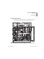
Figure 7 displays the pin layout of the I/O Connector in the 50-pin header,
located at position JP2 on the eZ80Acclaim!® Development Kit. Table 4
on page 17 identifies the pins and their functions.
UM014220-0508
eZ80 Development Kit
eZ80F91 Development Kit
User Manual
16
JP2
PB7
PB5
PB3
PB1
GND_EXT
PC6
PC4
PC2
PC0
PD6
PD5
PD3
PD1
TDO
GND_EXT
TCK
RTC_VDD
IICSCL
IICSDA
FLASHWE
CS3
RESET
V3.3_EXT
HALT_SLP
V3.3_EXT
1
3
5
7
9
11
13
15
17
19
21
23
25
27
29
31
33
35
37
39
41
43
45
47
49
2
4
6
8
10
12
14
16
18
20
22
24
26
28
30
32
34
36
38
40
42
44
46
48
50
PB6
PB4
PB2
PB0
PC7
PC5
PC3
PC1
PD7
GND_EXT
PD4
PD2
PD0
TDI
TRIGOUT
TMS
EZ80CLK
GND_EXT
DIS_IRDA
WAIT
GND_EXT
NMI
HEADER 25X2
IDC50
Figure 7. eZ80Acclaim!® Development Kit I/O Connector Pin Configuration—JP2
UM014220-0508
eZ80 Development Kit
eZ80F91 Development Kit
User Manual
17
Table 4. eZ80Acclaim! ® Development Kit I/O Connector Identification—JP21
Symbol
1
PB7
Bidirectional
Yes
2
PB6
Bidirectional
Yes
3
PB5
Bidirectional
Yes
4
PB4
Bidirectional
Yes
5
PB3
Bidirectional
Yes
6
PB2
Bidirectional
Yes
7
PB1
Bidirectional
Yes
8
PB0
Bidirectional
Yes
9
GND
10
PC7
Bidirectional
Yes
11
PC6
Bidirectional
Yes
12
PC5
Bidirectional
Yes
13
PC4
Bidirectional
Yes
14
PC3
Bidirectional
Yes
15
PC2
Bidirectional
Yes
16
PC1
Bidirectional
Yes
17
PC0
Bidirectional
Yes
18
PD7
Bidirectional
Yes
19
PD6
Bidirectional
20
GND
21
PD5
Bidirectional
Yes
22
PD4
Bidirectional
Yes
23
PD3
Bidirectional
Yes
UM014220-0508
Signal Direction
Active Level
eZ80F91 Signal2
Pin #
eZ80 Development Kit
eZ80F91 Development Kit
User Manual
18
Table 4. eZ80Acclaim! ® Development Kit I/O Connector Identification—JP21
Symbol
24
PD2
Bidirectional
Yes
25
PD1
Bidirectional
Yes
26
PD0
Bidirectional
Yes
27
TDO
Input
Yes
28
TDI/ZDA
Output
Yes
29
GND
30
TRIGOUT
Input
31
TCK/ZCL
Output
32
TMS
Output
33
RTC_VDD
34
EZ80CLK
35
SCL
36
GND
37
SDA
38
GND
39
FlashWE
40
GND
41
CS3
42
DIS_IrDA
43
RESET
44
WAIT
45
VDD
46
GND
UM014220-0508
Signal Direction
Active Level
eZ80F91 Signal2
Pin #
High
Yes
High
Yes
Input
Yes
Bidirectional
Yes
Bidirectional
Yes
Output
Low
No
Input
Low
Yes
Output
Low
No
Bidirectional
Low
Yes
Output
Pull-Up 10 kΩ; Low
Yes
eZ80 Development Kit
eZ80F91 Development Kit
User Manual
19
Table 4. eZ80Acclaim! ® Development Kit I/O Connector Identification—JP21
Pin #
Symbol
47
HALT_SLP
48
NMI
49
VDD
50
Reserved
Signal Direction
Active Level
eZ80F91 Signal2
Input
Low
Yes
Output
Low
Yes
Notes
1. For the sake of simplicity in describing the interface, Power and Ground nets are omitted from
this table. The entire interface is represented in the eZ80F91 Module Schematics, see Figure 23
through Figure 25.
2. The Power and Ground nets are connected directly to the eZ80F91 device.
Internal On-Chip Flash Memory
To program internal on-chip Flash memory, the JP3 shunt must be
installed. Table 5 lists the setting for the JP3 jumper that is resident on the
eZ80F91 Module.
Table 5. Jumper, eZ80F91 Module
Shunt
Symbol Jumper Name Status
JP3
Write Enable
(WR_EN)
Function
Affected Device
In
On-chip Flash is enabled for
writing.
On-chip Flash
Out
On-chip Flash memory is writeprotected.
On-chip Flash
Application Module Interface
An Application Module Interface is provided to allow you to add an application-specific module to the eZ80Acclaim!® Development Kit. Zilog’s
UM014220-0508
eZ80 Development Kit
eZ80F91 Development Kit
User Manual
20
Thermostat Application Module (not provided in the kit) is an example of
an application-specific module that demonstrates an HVAC control system. Implementing an application module with the Application Module
Interface requires that the eZ80F91 Module also be mounted on the
eZ80Acclaim! Development Kit, because the eZ80F91 device controls the
application. To mount an application module, use the two male headers J6
and J8.
Connector J6 carries the General-Purpose Input/Output ports (GPIO), and
connector J8 carries memory and control signals. To design an application
module, you must be familiar with the architecture and features of the
eZ80F91 Module currently installed. Table 6 and Table 7 list the signals
and functions related to each of these connectors by pin. Power and
ground signals are omitted for the sake of simplicity.
Table 6. GPIO Connector J6*
Signal
Pin #
Function
Direction
SCL
5
I2C Clock
IN/OUT
SDA
7
I2C
IN/OUT
MOD_DIS
9
Modem Disable
IN
MWAIT
13
WAIT signal for
the CPU
IN
EM_D0
15
Emulated, Bit 0
IN/OUT
CS3
17
Chip Select 3 of
the CPU
OUT
EM_D[7:1]
21,23,25, Emulated, Bit
27,29,31, [7:1]
33
Reserved
35
UM014220-0508
Data
Notes
If a shunt is installed between
pins 6 and 9, the modem
function on the eZ80Acclaim!®
Development Kit is disabled.
This signal is also present on
the J8.
IN/OUT
eZ80 Development Kit
eZ80F91 Development Kit
User Manual
21
Table 6. GPIO Connector J6* (Continued)
Signal
Pin #
Function
Direction
PC[7:0]
39,41,43, Port C, Bit [7:0]
45,47,49,
51,53
IN/OUT
ID_[2:0]
6,8,10
eZ80Acclaim!
Development Kit
ID
OUT
CON_DIS
12
Console Disable
IN
Reserved
16,18
PD[7:0]
22,24,26, Port D, Bit[7:0]
28,30,32,
34,36
IN/OUT
PB[7:0]
40,42,44, Port B, Bit[7:0]
46,48,50,
52,54
IN/OUT
Notes
If a shunt is installed between
pins 12 and 14, the Console
function on the eZ80Acclaim!
Development Kit is disabled.
Note: *All of the signals are driven directly by the CPU.
Table 7. CPU Bus Connector J8*
Signal
Pin #
Function
Direction
A[0:7]
3–10
Address Bus, Low Byte
OUT
A[8:15]
13–20
Address Bus, High Byte
OUT
A[16:23]
23–30
Address Bus, Upper Byte
OUT
RD
33
READ Signal
OUT
RESET
35
Push Button Reset
OUT
UM014220-0508
eZ80 Development Kit
eZ80F91 Development Kit
User Manual
22
Table 7. CPU Bus Connector J8* (Continued)
Signal
Pin #
Function
Direction
BUSACK
37
CPU Bus Acknowledge Signal
OUT
NMI
39
Nonmaskable Interrupt
IN
D[0:7]
43–50
Data Bus
IN/OUT
CS[0:3]
53–56
Chip Selects
MREQ
57
Memory Request
OUT
WR
34
Write Signal
OUT
INSTRD
36
Instruction Fetch
OUT
BUSREQ
38
CPU Bus Request signal
PHI
40
Clock output of the CPU
OUT
Note: *All of the signals except BUSACK and INSTRD are driven by low-voltage CMOS technology
(LVC) drivers.
I/O Functionality
The eZ80Acclaim!® Development Kit provides I/O functionality. These
functions are memory-mapped with an address decoder based on the
Generic Array Logic GAL22lV10D (U15) device manufactured by Lattice Semiconductor, and a bidirectional latch (U16). Additionally, U15 is
used to decode addresses for access to the 7 x 5 LED matrix.
Table 8 lists the addresses of registers that allow access to the above functions. The register at address 800000h controls GPIO Output Control and
LED Anode register functions. The register at address 800001h controls
the register functions for the LED cathode, modem reset, and user triggers.
Address 800002h contains GPIO data.
UM014220-0508
eZ80 Development Kit
eZ80F91 Development Kit
User Manual
23
Table 8. LED and Port Emulation Addresses
Address Register Function
Access
800000h LED Anode/GPIO Port output control
WR
800001h LED Cathode/Modem/Trig
WR
800002h GPIO Data
RD/WR
GPIO Emulation
GPIO is emulated with the use of the GPIO Output Control Register and
the GPIO Data Register. Table 9 lists the multiple functions of the register.
Table 9. LED Anode/GPIO Output Control Register
Bit #
Function
7
6
5
4
3
2
1
Anode Col 1
X
Anode Col 2
X
Anode Col 3
X
Anode Col 4
X
Anode Col 5
X
Anode Col 6
X
Anode Col 6
GPIO Output
0
X
X
The GPIO Data Register receives inputs or provides outputs for each of
the seven GPIO lines, depending on the configuration of the port. See
Table 10.
UM014220-0508
eZ80 Development Kit
eZ80F91 Development Kit
User Manual
24
Table 10. GPIO Data Register
Function/Bit #
7
6
5
4
3
2
1
GPIO D0
X
GPIO D1
X
GPIO D2
X
GPIO D3
X
GPIO D4
X
GPIO D5
X
GPIO D6
GPIO D7
0
X
X
Modem Reset
The Modem Reset signal, MRESET, is used to reset an optional socket
modem. This signal is controlled by bit 5 in the register shown in Table 15.
The MRESET signal is available at the embedded modem socket interface (J9, Pin 1). Setting this bit Low places the optional socket modem into
a reset state. You must pull this bit High again to enable the socket modem.
Reference the appropriate documentation for the socket modem to reset
timing requirements.
User Triggers
Two trigger output pins are provided on the eZ80Acclaim!® Development
Kit. Labeled J21 (Trig2) and J22 (Trig1), these pins allow you to trigger
external equipment to aid in the debug of the system. See Figure 8 for
trigger pin details.
UM014220-0508
eZ80 Development Kit
eZ80F91 Development Kit
User Manual
25
J21
J22
Ground
Trigger output
Trig2
Trig1
Figure 8. Trigger Pins J21 and J22
Bits 6 and 7 in Table 15 are the control bits for the user triggers. If either
bit is a 1, the corresponding Trig1 and Trig2 signals are driven High. If
either bit is 0, the corresponding Trig1 and Trig2 signals are driven Low.
Embedded Modem Socket Interface
The eZ80Acclaim! Development Kit features a socket for an optional 56
K modem (a modem is not included in the kit).
Connectors J1, J5, and J9 provide connection capability. The modem
socket interface provided by these three connectors is shown in Figure 9.
Table 11 through Table 13 identify the pins for each connector. The
embedded modem utilizes UART1, which is available via the Port C pins.
UM014220-0508
eZ80 Development Kit
eZ80F91 Development Kit
User Manual
26
J5
J1
1
2
2
4
24
25
26
27
J9
1
28
29
3
6
7
30
31
8
9
32
Figure 9. Embedded Modem Socket Interface—J1, J5, and J9
Table 11. Connector J5
Pin Symbol
Description
1
M-TIP
Telephone Line Interface—TIP
2
M-RING
Telephone Line Interface—RING
Table 12. Connector J9
Pin Symbol
Description
1
MRESET
Reset, active Low, 50–100 ms. Closure to GND for reset
3
GND
Ground
6
D1
DCD indicator; can drive an LED anode without additional circuitry
UM014220-0508
eZ80 Development Kit
eZ80F91 Development Kit
User Manual
27
Table 12. Connector J9 (Continued)
7
D2
RxD indicator; can drive an LED anode without additional circuitry
8
D3
DTR indicator; can drive an LED anode without additional circuitry
9
D4
TxD indicator; can drive an LED anode without additional circuitry
Table 13. Connector J1
Pin Symbol
Description
2
MOD_DIS
Modem disable, active Low
4
VCC
+5 VDC or +3.3 VDC input
24
GND
Ground
25
PC4_DTR1
DTR interface; TTL levels
26
PC6_DCD1
DCD interface; TTL levels
27
PC3_CTS1
CTS interface; TTL levels
28
PC5_DSR1
DSR interface; TTL levels
29
PC7_RI1
Ring Indicator interface; TTL levels
30
PC0_TXD1
TxD interface; TTL levels
31
PC1_RXD1
RxD interface; TTL levels
32
PC2_RTS1
RTS interface; TTL levels
Components P4, T1, C3, C4, and U11 provide the phone line interface to
the modem. On the eZ80Acclaim!® Development Kit, LEDs D1, D2, D3,
and D4 function as status indicators for this optional modem.
The phone line connection for the modem is for the United States only.
Connecting the modem outside of the U.S. requires modification.
UM014220-0508
eZ80 Development Kit
eZ80F91 Development Kit
User Manual
28
The tested modem for this eZ80F91 Development Kit is a MultiTech Systems (formerly Conexant) socket modem, part number SC56H1. Either the
3.3 V or the 5.0 V version of the modem can be used. However, jumper J12
should be configured accordingly—see Table 20. Information about this
modem and its interface is available in the SocketModem data sheet from
www.multitech.com.
eZ80Acclaim!® Development Kit Memory
Memory space on the eZ80Acclaim! Development Kit consists of
onboard SRAM and additional SRAM footprints.
Onboard SRAM
The eZ80Acclaim! Development Kit features 512 KB SRAM at U20.
This SRAM provides the basic memory requirement for small applications development. This SRAM is in the address range B80000h–
BFFFFFh. With the 512 KB of SRAM on the eZ80F91 Module, this
addressing structure provides 1 MB of contiguous SRAM for immediate
use. The Chip Select 2 (CS2) signal is used to access the 512 KB of
SRAM on the eZ80Acclaim! Development Kit.
Additional SRAM
The amount of eZ80Acclaim! Development Kit memory can be extended
if required by adding SRAM devices. U19, U18, and U17 provide this
capability. However, ensure that additional SRAM is installed in the following order:
1. U19, address range B00000h - B7FFFFh
2. U18, address range A80000h - AFFFFFh
3. U17, address range A00000h - A7FFFFh
If SRAM memory is installed in a different order than the above
sequence, SRAM will not be contiguous unless you are able to change the
address decoder, U10. Memory access decoding is performed by this
UM014220-0508
eZ80 Development Kit
eZ80F91 Development Kit
User Manual
29
address decoder, implemented in the Generic Array Logic device,
GAL22LV10D (U10).
On-Chip SRAM
The eZ80F91 device on the eZ80F91 Module contains 8 KB of on-chip
SRAM. Upon power-up, this SRAM is enabled and mapped to address
FFC000h. Using the RAM Address Register, this 8 KB memory can be
mapped to the top of any 64 KB block. It can also be disabled. Refer to
eZ80F91 MCU Product Specification (PS0192) for more information.
Flash Memory
The eZ80F91 Development Kit allows off-chip Flash memories between
1 MB and 4 MB. This Flash memory is entirely located on the eZ80F91
Module (as footprint only; as shipped from the factory, external Flash is
not installed).
Memory Map
A memory map of the eZ80Acclaim!® Development Kit and the eZ80F91
Module is displayed in Figure 10. Flash memory and SRAM on the
eZ80F91 Module are addressed when CS0 and CS1 are active Low.
SRAM on the eZ80Acclaim! Development Kit is addressed when CS2 is
active Low.
Refer to eZ80F91 MCU Product Specification (PS0192) for more details
about controlling on-chip Flash memory and SRAM.
UM014220-0508
eZ80 Development Kit
eZ80F91 Development Kit
User Manual
30
On-chip
SRAM
FFFFFFh
FFE000h
8 KB
Available
Address Space
DFFFFFh
SRAM Memory
up to 2 MB
C7FFFFh
C00000h
BFFFFFh
B80000h
CS1
Module SRAM
Platform SRAM (512 KB)
Platform Expansion
SRAM Memory up to 4 MB
80FFFFh
800000h
CS2
LED & GPIO
7FFFFFh
Off-module
Flash memory
Expansion Module:
Flash Memory up to 4 MB
Up to 4 MB
400000h
3FFFFFh
Expansion Module
Flash Memory up to 4 MB
Off-chip
Flash memory
on the module
CS0 (8 MB)
200000h
120000h
11FFFFh
1FFFFFh
Flash Memory
Up to 4 MB
1 MB
040000h
100000h
On-chip
Flash memory
03FFFFh
000000h
256 KB
Figure 10. Memory Map of the eZ80Acclaim!® Development Kit and eZ80F91 Module
UM014220-0508
eZ80 Development Kit
eZ80F91 Development Kit
User Manual
31
Chip Selects and Wait States—As seen in the memory map in
Figure 10, Flash memory is enabled by CS0, on-module SRAM is
enabled by CS1, and the remainder of the resources are enabled by CS2.
The number of wait states (N) for each Chip Select are indicated in
Table 14.
Table 14. Chip Select Wait States
Memory Type
CS0
CS1
CS2
CS3
Flash
N=7
*
*
*
On-module SRAM
*
N=1
*
*
eZ80Acclaim!® Development Kit SRAM
*
*
N=2
*
and other resources
Note: *Not applicable for these resources.
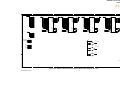
LEDs
As mentioned in Table 13, LEDs D1, D2, D3, and D4 function as status
indicators for an optional modem. This section describes each LED and
the LED matrix device.
LED Matrix
The 7 x 5 LED matrix device on the eZ80Acclaim!® Development Kit is a
memory-mapped device that can be used to display information, such as
programmed alphanumeric characters. For example, the LED display
sample program that is shipped with this kit displays the alphanumeric
message:
eZ80
To illuminate any LED in the matrix, its respective anode bit must be set
to 1 and its corresponding cathode bit must be set to 0.
UM014220-0508
eZ80 Development Kit
eZ80F91 Development Kit
User Manual
32
Bits 0–6 in Table 9 are LED anode bits. They must be set High (1) and
their corresponding cathode bits, bits 0–4 in Table 15, must be set Low (0)
to illuminate each of the LED’s, respectively.
If bit 7 in the GPIO Output Control Register is 1, all of the GPIO lines are
configured as inputs. If this bit is 0, all of the GPIO lines are configured as
outputs.
Table 15 indicates the multiple register functions of the LED cathode,
modem, and triggers. This table shows the bit configuration for each cathode bit. Bits 5, 6, and 7 do not carry any significance within the LED
matrix. These three bits are control bits for the modem reset, Trig1, and
Trig2 functions, respectively.
Table 15. Bit Access to the LED Cathode, Modem, and Triggers
Bit #
Function
7
6
5
4
3
2
1
Cathode Row 5
X
Cathode Row 4
X
Cathode Row 3
X
Cathode Row 2
X
Cathode Row 1
X
Modem RST
X
Trig 1
Trig 2
0
X
X
An LED display sample program is shipped with the eZ80F91 Development Kit. Refer to eZ80Acclaim!®Development Kits Quick Start Guide
(QS0020) or to the Tutorial section in the Zilog Developer Studio II—
eZ80Acclaim!® User Manual (UM0144).
UM014220-0508
eZ80 Development Kit
eZ80F91 Development Kit
User Manual
33
Data Carrier Detect
The Data Carrier Detect (DCD) signal at D1 indicates that a good carrier
signal is being received from the remote modem.
RX
The RX signal at D2 indicates that data is received from the modem.
Data Terminal Ready
The Data Terminal Ready (DTR) signal at D3 informs the modem that the
PC is ready.
TX
The TX signal at D4 indicates that data is transmitted to the modem.
Push Buttons
The eZ80Acclaim!® Development Kit provides user controls in the form
of push buttons. These push buttons serve as input devices to the eZ80F91
device. You can use them as necessary for application development. All
push buttons are connected to the GPIO Port B pins.
PB0
The PB0 push button switch, SW1, is connected to bit 0 of GPIO Port B.
This switch can be used as the port input if required.
PB1
The PB1 push button switch, SW2, is connected to bit 1 of GPIO Port B.
This switch can be used as the port input if required.
PB2
The PB2 push button switch, SW3, is connected to bit 2 of GPIO Port B.
This switch can be used as the port input if required.
UM014220-0508
eZ80 Development Kit
eZ80F91 Development Kit
User Manual
34
RESET
The Reset push button switch, SW4, resets the eZ80® CPU and the
eZ80Acclaim!® Development Kit.
Jumpers
The eZ80Acclaim! Development Kit provides a number of jumpers that
are used to enable or disable functionality on the platform, enable or disable optional features, or to provide protection from inadvertent use.
Jumper J2
The J2 jumper connection enables/disables IrDA transceiver functionality. When the shunt is placed, IrDA communication is disabled. See
Table 16.
Table 16. J2—DIS_IrDA
Shunt
Status Function
Affected Device
IN
IrDA on eZ80F91 UART0 is configured to work with the RS-232 or the RS-485
Module disabled interfaces.
OUT
IrDA on eZ80F91 IrDA is enabled to work with UART0 on the eZ80F91 device.
Module enabled
Jumper J3
The J3 jumper connection controls GPIO emulation mode and communication with the 7 x 5 LED. When the shunt is placed, GPIO emulation is
disabled. See Table 17.
UM014220-0508
eZ80 Development Kit
eZ80F91 Development Kit
User Manual
35
Table 17. J3—DIS_EM
Shunt
Status
Function
Affected Device
IN
Application Module Communication with 7 x 5 LED and Port emulation circuit
Hardware Disabled is disabled.
OUT
Application Module Communication with 7 x 5 LED and Port A emulation circuit
Hardware Enabled is enabled.
Jumper J7
The J7 jumper connection controls Flash boot loader programming. When
the shunt is placed, overwriting of the Flash boot loader program is
enabled. See Table 18.
Table 18. J7—FlashWE (Off-Chip)*
Shunt
Status
Function
Affected Device
OUT
The Flash boot sector of the eZ80F91
Module is write-protected.
Flash boot sector of the eZ80F91
Module.
IN
The Flash boot sector of the eZ80F91
Module is enabled for writing or
overwriting.
Flash boot sector of the eZ80F91
Module.
Note: As shipped from the factory, external Flash memory is not installed.
Jumper J11
The J11 jumper connection controls access to the off-chip Flash memory
device. When the shunt is placed, access to this Flash device is enabled.
See Table 19.
UM014220-0508
eZ80 Development Kit
eZ80F91 Development Kit
User Manual
36
The silk-screened label on the eZ80Acclaim!® Development Kit
Note: for jumper J11 is incorrect. Currently, it reads DIS_FLASH. The
correct label is EN_FLASH.
Table 19. J11—EN_FLASH (Off-Chip)*
Shunt
Status
Function
Affected Device
IN
All access to external Flash memory on the External Flash memory on the
eZ80190 Module is enabled.
eZ80190 Module.
OUT
All access to external Flash memory on the External Flash memory on the
eZ80190 Module is disabled.
eZ80190 Module.
Note: As shipped from the factory, external Flash memory is not installed.
Jumper J12
The J12 jumper connection controls the selection of a 5 V or 3 VDC
power supply to the embedded modem, if an embedded modem is used.
See Table 20.
Table 20. J12—5 VDC/3.3 VDC for an Embedded Modem
Shunt
Status
Function
Affected Device
1–2
5 VDC is provided to power the embedded modem.
Embedded modem.
2–3
3.3 VDC is provided to power the embedded modem. Embedded modem.
UM014220-0508
eZ80 Development Kit
eZ80F91 Development Kit
User Manual
37
Jumper J14
The J14 jumper connection controls the polarity of the Ring Indicator. See
Table 21.
Table 21. J14—RI
Shunt Status
Function
Affected Device
1–2
The Ring Indicator for UART1 is inverted.
UART1
2–3
The Ring Indicator for UART1 is not
inverted.
UART1
Jumper J15
The J15 jumper connection controls the selection RS-485 circuit along
with UART0. When the shunt is placed, the RS-485 circuit is enabled.
See Table 22. RS-485 functionality will be available in future eZ80®
devices.
Table 22. J15—RS485_1_EN*
Shunt
Status
Function
Affected Device
IN
The RS-485 circuit is enabled on UART0.
The UART0 CONSOLE interface and IrDA are
disabled.
IrDA, UART0 CONSOLE
interface, RS-485 interface.
OUT
The RS-485 circuit is disabled on UART0.
IrDA, UART0 CONSOLE
interface, RS-485 interface.
Note: *To enable the RS-485 circuit, the corresponding IrDA/RS-232 circuit must be disabled.
Jumper J16
The J16 jumper connection controls the selection of the RS-485 circuit.
However, UART1 MODEM interface and the socket modem interface are
UM014220-0508
eZ80 Development Kit
eZ80F91 Development Kit
User Manual
38
disabled if the RS-485 circuit is enabled. When the shunt is placed, the
RS-485 circuit is enabled. See Table 23.
Table 23. J16—RS485_2_EN
Shunt
Status
Function
Affected Device
IN
The RS-485 circuit is enabled on UART1.
The UART1 MODEM interface and the
Socket Modem interface are disabled.
UART1 MODEM interface,
Socket Modem Interface, and
RS-485 interface.
OUT
The RS-485 circuit is disabled on UART1.
UART1 MODEM interface,
Socket Modem Interface, and
RS-485 interface.
Jumper J17
The J17 jumper connection controls the selection of the RS-485 termination resistor circuit. When the shunt is placed, the RS-485 termination
resistor circuit is enabled. See Table 24.
Table 24. J17—RT_1*
Shunt
Status
Function
Affected Device
IN
The Termination Resistor for RS485_1 is IN.
RS-485 interface.
OUT
The Termination Resistor for RS485_1 is OUT.
RS-485 interface.
Note: *Before enabling the termination resistor, ensure that the device is located at the end of the
interface line.
Jumper J18
The J18 jumper connection controls the selection of the RS-485 termination resistor circuit. When the shunt is placed, the RS-485 termination
resistor circuit is enabled. See Table 25.
UM014220-0508
eZ80 Development Kit
eZ80F91 Development Kit
User Manual
39
Table 25. J18—RT_2*
Shunt
Status
Function
Affected Device
IN
The Termination Resistor for RS485_2 is IN.
RS-485 interface.
OUT
The Termination Resistor for RS485_2 is OUT.
RS-485 interface.
Note: *Before enabling the termination resistor, ensure that the device is located at the end of the
interface line.
Jumper J19
The J19 jumper connection selects the range of memory addresses for the
external chip select signal, CS_EX, to the application module. See
Table 26.
Table 26. J19—EX_SEL
Shunt
Status
Function
Affected Device
1–2
CS_EX is decoded in the CS0 memory space and is Application module
located in the address range 400000h–7FFFFFh.
addressing.
3–4
CS_EX is decoded in the CS2 memory space and is Application module
located in the address range A00000h–A7FFFFh.
addressing.
5–6
CS_EX is decoded in the CS2 memory space and is Application module
located in the address range A80000h–AFFFFFh.
addressing.
7–8
CS_EX is decoded in the CS2 memory space and is Application module
located in the address range B00000h–B7FFFFh.
addressing.
UM014220-0508
eZ80 Development Kit
eZ80F91 Development Kit
User Manual
40
Jumper J20
The J20 jumper connection controls the selection of the external chip
select in the external application module. When the shunt is placed, the
external chip select signal, CS_EX, is disabled. See Table 27.
Table 27. J20—EX_FL_DIS
Shunt
Status
Function
Affected Device
IN
The jumper for EX_FL_DIS is IN.
The chip select on the application module
is disabled.
OUT
The jumper for EX_FL_DIS is OUT. The chip select on the application module
is enabled.
Connectors
A number of connectors are available for connecting external devices
such as the ZPAK II Debug Tool, PC serial ports, external modems, the
console, and LAN/telephone lines.
J6 and J8 are the headers, or connectors, that provide pin-outs to connect
any external application module, such as Zilog’s Thermostat Application
Module.
Connector J6
The J6 connector provides pin-outs to make use of GPIO functionality.
Connector J8
The J8 connector provides pin-outs to access memory and other control
signals.
UM014220-0508
eZ80 Development Kit
eZ80F91 Development Kit
User Manual
41
Console
Connector P2 is the RS-232 terminal, which can be used for observing the
console output. P2 can be connected to the PC running HyperTerminal, if
required.
Modem
Connector P3 provides a terminal for connecting an external modem, if
used with the eZ80F91 Development Kit.
I2C Devices
The two I2C devices on the eZ80Acclaim!® Development Kit are the U2
EEPROM and the U13 Configuration register. The EEPROM provides 16
KB of memory. The Configuration register provides access to control the
configuration of an application-specific function at the Application Module Interface. Neither device is utilized by the eZ80F91 Development Kit
software. You are free to develop proprietary software for these two
devices. The addresses for accessing these devices are listed in Table 28.
Table 28. I2C Addresses
Device/Bit #
7
6
5
4
3
2
1
0
EEPROM (U10)*
1
0
1
0
0
A1
A0
R/W
Configuration Register (U13)
1
0
0
1
1
1
0
R/W
Note: *EEPROM address bits A0 and A1 are configured for 0s.
UM014220-0508
eZ80 Development Kit
eZ80F91 Development Kit
User Manual
42
eZ80F91 Module
This section describes the eZ80F91 Module hardware, its interfaces and
key components, including the CPU, real-time clock, IrDA transceiver,
and memory.
Functional Description
The eZ80F91 Module is a compact, high-performance module specially
designed for the rapid development and deployment of embedded systems. Additional devices such as serial ports, LED matrices, GPIO ports,
and I2C devices are supported when connected to the eZ80Acclaim!®
Development Kit. A block diagram representing both of these boards is
shown in Figure 1 on page 4.
Despite its small footprint, the eZ80F91 Module provides a CPU, Flash
memory, Ethernet interface, SRAM, an IrDA transceiver, and a real-time
clock with a back-up battery. This module is powered by the eZ80F91
microcontroller, a new member of eZ80® product family. The eZ80F91
Module can also be used as a stand-alone development tool when provided with an external power source.
The eZ80F91 Module is equipped with an Am79C874 PHY from AMD.
This PHY supports a number of different frequencies and types of communication, from 10 MB half-duplex to 100 MB full-duplex. There are
four resistors on the Module that control settings for the requested mode
of operation; these resistors are labelled R19, R21, R23, and R24. For
details, refer to eZ80F91 Module Product Specification (PS0193).
Fast Buffer
A Fast Buffer is located on the data bus to Flash memory. The purpose of
this Fast Buffer is to avoid bus contention that can exist due to the slow
turn-off time of Flash memory and the fast bus turn-around time of the
UM014220-0508
eZ80F91 Module
eZ80F91 Development Kit
User Manual
43
eZ80F91 device (a generic feature of the eZ80® family when it is used in
native mode). The discussion that follows references Figure 11.
Bus contention can occur when two or more devices drive a common bus.
CS0 on the eZ80F91 device drives the Flash CE. Upon accessing Flash
memory, CS0 is driven High a maximum of 8.8 ns after the next rising
edge of the CPU Clock (T6—refer to the External Memory Read Timing
diagram in the eZ80F91 MCU Product Specification (PS0192) for assistance). The Flash turn-off time (TOD) is 25 ns—the duration from OE or
CE going High to Flash output drivers in a high-impedance state. For further information, refer to MT28F008 data sheet on www.micron.com.
T6
CPU Clock
T3
CS0
Data In
eZ80F91 Data Bus
Data Out
RD
Bus Contention
TOD
Flash Data Bus
CS1
WR
T4
Figure 11. Possible Bus Contention without Fast Buffer
UM014220-0508
eZ80F91 Module
eZ80F91 Development Kit
User Manual
44
Essentially, after the eZ80F91 device accesses Flash memory, a time
duration of 8.8 ns + 25 ns = 33.8 ns can transpire before Flash memory
stops driving the data bus. At that time, the eZ80F91 device is well into
the next bus cycle. Assuming this next cycle is the Memory Write cycle,
then the data output of the eZ80F91 device is valid not later than T3 = 7.5
ns, and the write pulse is asserted not later than 4.5 ns after the falling
edge of the CPU Clock (14.5 ns from the rising edge if the CPU Clock is
50 MHz). The duration of bus contention, TCON, is 33.8 ns – 7.5 ns =
26.3 ns. Refer to the External Memory Write Timing diagram in the
eZ80F91 Product Specification (PS0192) for assistance.
With the addition of a Fast buffer, Flash turn-off time is reduced from 25
ns to 5.5 ns. Bus contention can still occur, but the amount of time it consumes is not TCON = 26.3 ns but rather TCON = (8.8 ns – 7.5 ns + 5.5 ns)
= 6.8 ns. At this faster rate, data that is being written does not become
corrupted because the write pulse is not yet asserted.
As of the date of publication of this document, Zilog has not completed an
analysis of the effect that this 6.8 ns period of bus contention has on the
design. An Application Note from Cypress Semiconductor titled NoBL
SRAM and Bus Contention further explains this bus contention issue.
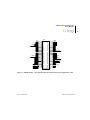
Physical Dimensions
The footprint of the eZ80F91 Module PCB is 63.5 mm x 78.7 mm. With
an RJ-45 Ethernet connector, the overall height is 25 mm. See Figure 12.
UM014220-0508
eZ80F91 Module
eZ80F91 Development Kit
User Manual
45
16.5 mm
56.0 mm
eZ80F91 MODULE
JP1
JP2
1
2
R15
R23
R16
R24
R25
Y1
1
R14
R21
R13
R19
R28
ZiLOG PCA: 99C0879-001
COPYRIGHT ZiLOG XTOOLS 2002
U6
+
P2
JP3
ISO
R17
R18
R36
R22
R20
CR1
VL1
U8
78.7 mm
C21
C20
C19
C18
Y2
C40
U5
C22
Y3
U4
C12
C11
U1
R37
R3
C3
R10
R4
R6
C42
U2
C1
R29
U3
31.8 mm
63.5 mm
Figure 12. Physical Dimensions of the eZ80F91 Module
UM014220-0508
eZ80F91 Module
eZ80F91 Development Kit
User Manual
46
Figure 13 displays the top layer silkscreen of the eZ80F91 Module.
eZ80F91 MODULE
JP1
JP2
1
2
Y1
1
R15
R14
R23
R21
R16
R13
R24
R19
R25
R28
U6
R17
JP3
ZiLOG PCA: 99C0879-001
P2
CR1
R18
R36
ISO
R22
VL1
R20
U8
COPYRIGHT ZiLOG XTOOLS 2002
+
C21
C20
C19
C18
Y2
C40
U5
C22
Y3
U4
U1
R37
C12
C11
R3
C3
R4
R6
C42
R10
U2
C1
R29
U3
Figure 13. eZ80F91 Module—Top Layer
UM014220-0508
eZ80F91 Module
eZ80F91 Development Kit
User Manual
47
Figure 14 displays the bottom layer silkscreen of the eZ80F91 Module.
JP2
R35
DJP 2002
JP1
R34
2
1
C4
C7
C16
C13
C14
C50
C49
C48
C47
C53
C51
C52
C39
R11
R33
R31
R32
C17
C15
C44
C45
C46
C34
C35
C33
C26
C29
C27
C25
C36
L1
U9
C32
C9
C28
C31
C30
C10
C8
R9
R27
C24
C38
C5
R26
C23
R8
C6
C37
C43
R2
U10
R7
R1
R30
R12
C41
R5
C2
MADE IN U.S.A.
ZiLOG FAB: 98C0879-001 REV A
Figure 14. eZ80F91 Module—Bottom Layer
Operational Description
The purpose of the eZ80F91 Module as a feature of the eZ80F91 Development Kit is to provide a plug-in tool to evaluate such features of the
eZ80F91 device as on-chip EMAC, SRAM, Flash, etc.
UM014220-0508
eZ80F91 Module
eZ80F91 Development Kit
User Manual
48
eZ80F91 Module Memory
Static RAM
The eZ80F91 Module features 512 KB of fast SRAM. Access speed is
typically 12 ns, allowing zero-wait-state operation at 50 MHz. With the
CPU at 50 MHz, SRAM can be accessed with zero wait states in eZ80
mode. CS1_CTL (CS1) can be set to 08h (no wait states).
Flash Memory
The eZ80F91 Module features 256 KB of on-chip Flash memory, which
can be programmed a single byte at a time, or in bursts of up to 128 bytes.
Write operations can be performed using either memory or I/O instructions. Erasing bytes in Flash memory returns them to a value of FFh. Both
the MASS ERASE and PAGE ERASE operations are self-timed by the
Flash controller, leaving the CPU free to execute other operations in parallel. Upon power-up, the on-chip Flash memory is located in the address
range 000000h–03FFFFh. Four wait states are programmed in Flash
control register F8h.
On-chip Flash memory is prioritized over all external Chip Selects, can be
enabled or disabled (power-on enabled), and can be programmed within
any 256 KB address space in the 16 MB address range.
The eZ80F91 Module features the following memory configurations:
•
•
•
On-chip SRAM: 8 KB
Off-chip SRAM: 512 KB
On-chip Flash: 256 KB
Reset Generator
An onboard supervisory chip is connected to the eZ80F91 Reset input
pin. It performs reliable Power-On Reset functions, generating a reset
pulse with a duration of 200 ms if the power supply drops below 2.93 V.
This reset pulse ensures that the board always starts in a defined
UM014220-0508
eZ80F91 Module
eZ80F91 Development Kit
User Manual
49
condition. The RESET pin on the I/O connector reflects the status of the
RESET line. It is a bidirectional pin for resetting external peripheral
components or for resetting the eZ80F91 Development Kit with a lowimpedance output (for example, a 100 Ω push button).
IrDA Transceiver
An onboard IrDA transceiver (ZHX1810) is connected to PD0 (TX), PD1
(RX), and PD2 (Shutdown, IR_SD). The IrDA transceiver is of the LED
type 870 nm Class 1.
The IrDA transceiver is accessible via the IrDA controller attached to
UART0 on the eZ80F91 device. While using the IrDA transceiver, you
must disable the console port on the eZ80Acclaim!® Development Kit.
See Table 6 on page 20.
To use the UART0 as a console or to save power, the transceiver can be
disabled by the software or by an off-board signal when using the proper
jumper selection. The transceiver is disabled by setting PD2 (IR_SD)
High or by pulling the DIS_IRDA pin on the I/O connector Low. The
shutdown feature is used for power savings. To enable the IrDA transceiver, DIS_IRDA is left floating and PD2 is pulled Low.
The RxD and TxD signals on the transceiver perform the same functions
as a standard RS-232 port. However, these signals are processed as IrDA
3/16 coding pulses (sometimes called IrDA encoder/decoder pulses).
When the IrDA function is enabled, the final output to the RxD and TxD
pins are routed through the 3/16 pulse generator.
Another signal that is used in the eZ80F91 Module’s IrDA system is
Shut_Down (SD). The SD pin is connected to PD2 on the eZ80F91 Module. The IrDA control software on the wireless device must enable this
pin to wake the IrDA transceiver. The SD pin must be set Low to enable
the IrDA transceiver. On the eZ80F91 Module, a two-input OR gate is
used to allow an external pin to shut down the IrDA transceiver. Both pins
must be set Low to enable this function.
UM014220-0508
eZ80F91 Module
eZ80F91 Development Kit
User Manual
50
Figure 15 displays the eZ80F91 Module IrDA hardware connections.
External Disable
IrDA
eZ80F91
Device
PD2(IR_SD)
SD
PD1(RxD)
RD
PD0(TxD)
TD
Figure 15. IrDA Hardware Connections
The eZ80F91 Module features an Infrared Encoder/Decoder register that
configures the IrDA function. This register is located at address 0BFh in
the internal I/O register map.
The Infrared Encoder/Decoder register contains three control bits. Bit 0
enables or disables the IrDA encoder/decoder block. Bit 1, if it is set,
enables received data to pass into the UART0 Receive FIFO data buffer.
Bit 2 is a test function that provides a loopback sequence from the TxD
pin to the RxD input.
Bit 1, the Receive Enable bit, is used to block data from filling up the
Receive FIFO when the eZ80F91 Module is transmitting data. Because
IrDA signal passes through the air as its transmission medium, transmitted data can also be received. This Receive Enable bit prevents this data
from being received. After the eZ80F91 Module completes transmitting,
this bit is changed to allow for incoming messages.
The code that follows provides an example of how this function is
enabled on the eZ80F91 Module.
UM014220-0508
eZ80F91 Module
eZ80F91 Development Kit
User Manual
51
//Init_IRDA
// Make sure to first set PD2 as a port bit, an output and set it Low.
PD_ALT1 &= 0xFC;
PD_ALT2 |= 0x03;
UART_LCTL0= 0x80;
BRG_DLRL0=0x2F;
BRG_DLRH0=0x00;
UART_LCTL0=0x00;
UART_FCTL0=0xC7;
UART_LCTL0=0x03;
IR_CTL = 0x03;
//
//
//
//
//
//
//
//
//
//
PD0 = uart0tx, PD1 = uart0_rx
Enable alternate function
Select dlab to access baud rate generator
Baud rate Masterclock/(16*baudrate)
High byte of baud rate
Disable dlab
Clear tx fifo, enable fifo
8bit, N, 1 stop
enable IRDA Encode/decode and Receive
enable bit.
//IRDA_Xmit
IR_CTL = 0x01;
Putchar(0xb0);
//Disable receive
//Output a byte to the uart0 port.
Flash Loader Utility
The Flash Loader utility integrated within ZDS II provides a convenient
way to program on-chip Flash memory. Refer to Zilog Developer Studio
II—eZ80Acclaim!® User Manual (UM0144) for more details.
Mounting the Module
The eZ80F91 Module features two 60-pin connectors. However, the
eZ80Acclaim!® Development Kit contains 50-pin sockets for this module. When mounting the eZ80F91 Module onto the eZ80Acclaim! Development Kit, check its orientation to the platform to ensure a correct fit.
Observe the underside of the module to note that pin 60 of the JP2 connector is removed and that its corresponding socket on the eZ80Acclaim!
Development Kit is plugged.
Pin 60 of the eZ80F91 Module’s JP1 connector must align with the pin 50
socket on the eZ80Acclaim! Development Kit’s JP1 connector; pin 60 of
the eZ80F91 Module’s JP2 connector must align with pin 50 of the
UM014220-0508
eZ80F91 Module
eZ80F91 Development Kit
User Manual
52
eZ80Acclaim! Development Kit’s JP2 socket. When the module is
mounted correctly, it will overhang the edge of the eZ80Acclaim! Development Kit by 10 pins.
Changing the Power Supply Plug
The universal 9 VDC power supply offers three different plug configurations and a tool that aids in removing one plug configuration to insert
another, as shown in Figure 16.
Figure 16. 9 VDC Universal Power Supply Components
Note: Figure 16 is for the 9 VDC power supply. The 6 VDC power supply
might look different.
Follow the steps below to exchange one plug configuration for another:
1. Place the tip of the removal tool into the round hole at the top of the
current plug configuration.
2. Press down to disengage the keeper tab and push the plug configuration out of its slot.
3. Select the plug configuration appropriate for your location, and insert
it into the slot formerly occupied by the previous plug configuration.
4. Push the new plug configuration down until it snaps into place, as
indicated in Figure 17.
UM014220-0508
eZ80F91 Module
eZ80F91 Development Kit
User Manual
53
Figure 17. Inserting a New Plug Configuration
Note: Figure 17 is for the 9 VDC power supply. The 6 VDC power supply
might look different.
UM014220-0508
eZ80F91 Module
eZ80F91 Development Kit
User Manual
54
ZPAK II
ZPAK II is a debug tool used to develop and debug hardware and software. It is a networked device featuring an Ethernet interface and an RS232 console port. ZPAK II is shipped with a preconfigured IP address that
can be changed to suit the user on a local network. For more information
on using and configuring ZPAK II, refer to eZ80Acclaim!® Development
Kits Quick Start Guide (QS0020) and ZPAK II Product User Guide
(PUG0015).
ZDI Target Interface Module
The ZDI Target Interface Module provides a physical interface between
ZPAK II and the eZ80Acclaim!® Development Kit. The TIM module
supports ZDI functions. For more information on using the TIM module
or ZDI, refer to eZ80Acclaim!® Development Kits Quick Start Guide
(QS0020) and eZ80F91 Module Product Specification (PS0193).
JTAG
Connector P1 is the JTAG connector on the eZ80Acclaim! Development
Kit. JTAG will be supported in the next offering of eZ80® products.
Application Modules
Zilog® offers the Thermostat Application module, which can be used for
evaluating and developing process control and simple I/O applications.
The Thermostat Application module is equipped with an LCD display
that can be used to display process control and other physical parameters.
For additional reading about the Thermostat application, refer to Java
Thermostat Demo Application Note (AN0104) available for download at
www.zilog.com.
UM014220-0508
ZPAK II
eZ80F91 Development Kit
User Manual
55
ZDS II
Zilog Developer Studio II (ZDS II) Integrated Development Environment
is a complete stand-alone system that provides a state-of-the-art development environment. Based on the Windows® Vista/Win 98SE/Win2000SP4/WinXP Professional user interfaces, ZDS II integrates a languagesensitive editor, project manager, C-Compiler, assembler, linker, librarian,
and source-level symbolic debugger that supports the eZ80F91 device.
UM014220-0508
ZDS II
eZ80F91 Development Kit
User Manual
56
Troubleshooting
Overview
Before contacting Zilog Customer Support to submit a problem report,
follow these simple steps. If a hardware failure is suspected, contact a
local Zilog representative for assistance.
Cannot Download Code
If you are unable to download code to RAM using ZDS, ensure to press
and release the Reset button on the eZ80Acclaim!® Development Kit
prior to selecting Debug → Reset and then Debug → Go in ZDS II.
IrDA Port Not Working
If you plan to use the IrDA transceiver on the eZ80F91 Module, ensure
that the hardware is set up as follows:
UM014220-0508
•
Jumper J2 must be OFF (to enable the control gate that drives the
IrDA device).
•
Set port pin PD2 Low. When this port pin and Jumper J2 are turned
OFF, the IrDA device is enabled.
•
Install a jumper on connector J6 across pin names con_dis and GND
to disable the console serial port driver.
Troubleshooting
eZ80F91 Development Kit
User Manual
57
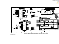
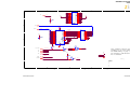
Schematics
eZ80F91 Development Platform
Figure 18 through Figure 22 displays the layout of the eZ80F91 Development Platform.
5
4
9VDC
SCL
SDA
D
1
3
5
7
9
11
13
15
17
19
21
23
25
27
29
31
33
35
37
39
41
43
45
47
49
51
53
55
57
59
GND
-MOD_DIS
-MWAIT
EM_D0
-CS3
GND
EM_D7
EM_D6
EM_D5
EM_D4
EM_D3
EM_D2
EM_D1
GND
PC7_RI1
PC6_DCD1
PC5_DSR1
PC4_DTR1
PC3_CTS1
PC2_RTS1
PC1_RXD1
PC0_TXD1
C
GND
GND
A8
A10
A12
A14
GND
A16
A18
A20
A22
VDD
-RESET
-BUSACK
-NMI
GND
D0
D2
D4
D6
GND
-CS0
-CS2
-MEMRQ VDD
-RST
ID_2
ID_1
ID_0
-CON_DIS
GND
-DIS_ETH
GND
PD7_RI0
PD6_DCD0
PD5_DSR0
PD4_DTR0
PD3_CTS0
PD2_RTS0
PD1_RXD0
PD0_TXD0
GND
PB7_MOSI
PB6_MISO
PB5_T5_O
PB4_T4_O
PB3_SCK
PB2_SS
PB1_T1_I PB2_SS
PB0_T0_I PB1_T1_I
PB0_T0_I
A1
A3
A5
A7
GND
A9
A11
A13
A15
VDD
R3
10K
GND
A17
A19
A21
A23
-CS1
-CS_EX
-IORQ
J4
VDD
1
3
5
GND
VDD
1OE
2OE
VCC
GND
20
10
2
4
6
8
11
13
15
17
A1
A2
A3
A4
A5
A6
A7
A8
GND
1
19
1OE
2OE
Y1
Y2
Y3
Y4
Y5
Y6
Y7
Y8
18
16
14
12
9
7
5
3
VCC
GND
20
10
TVCC_RESETn
VDD
1
3
5
7
9
11
13
1
2
4
6
8
10
12
14
DTR
1
GND
R20
0
2
GND
A8
A9
A10
A11
A12
A13
A14
A15
2
U21
HEADER 2
-M_CS0
-M_CS1
-M_CS2
-M_IORQ
-M_MEMRQ
-M_WR
-M_RD
-M_CS3
M_PHI
VDD
GND
C31
0.1uF
A16
A17
A18
A19
A20
A21
A22
A23
GND
4
2
3
4
5
6
7
8
9
10
11
A1
A2
A3
A4
A5
A6
A7
A8
A9
A10
Y1
Y2
Y3
Y4
Y5
Y6
Y7
Y8
Y9
Y10
23
22
21
20
19
18
17
16
15
14
1
13
OE1
OE2
VCC
GND
24
12
-CS0
-CS1
-CS2
-IORQ
-MEMRQ
-WR
-RD
-CS3
PHI
C
VDD
GND
C34
0.1uF
74LVC827/SO
VDD
GND
J12
VCC
C33
0.1uF
1
2
3
VDD
1
2
3
4
5
6
7
8
9
1
2
3
4
5
6
7
8
9
10
11
12
13
14
15
16
17
18
19
20
21
22
23
24
25
26
27
28
29
30
31
32
MODEM's
AGND
-MOD_DIS
D[7:0]
U7
D[7:0]
VCC
MD0
MD1
MD2
MD3
MD4
MD5
MD6
MD7
-M_RD
-L_RD
2
3
4
5
6
7
8
9
A0
A1
A2
A3
A4
A5
A6
A7
1
19
DIR
OE
B0
B1
B2
B3
B4
B5
B6
B7
18
17
16
15
14
13
12
11
VCC
GND
20
10
D0
D1
D2
D3
D4
D5
D6
D7
B
VDD
C1
0.1uF
74LVC245/SO
GND
MD[7:0]
MD0
MD1
MD2
MD3
MD4
MD5
MD6
MD7
VCC
VCC
GND
PC4_DTR1
PC6_DCD1
PC3_CTS1
PC5_DSR1
PC7_RI1
PC0_TXD1
PC1_RXD1
PC2_RTS1
VDD
GND
VDD
GND
Connectors
A
ZiLOG
910 E. Hamilton Avenue
Title
HEADER 9
0
HEADER 32
Schematic, eZ80L92 Evaluation Board
MODEM CONNECTORS
con 7x2
5
D
GND
-FLASHWE
GND
1
2
R21
TX D4
1
-MRESET
0
2
D3
TMS
PRSTn
TRIGOUT
-MRESET
R8
0
R9
RX D2
P1
TDI
TDO
TCK
4
3
J1
1
2
J9
2
7
GND
WP NC
Header 3
J5
M_TIP
M_RING
PRSTn
TCK
TDI
1
VDD
SCL
HEADER 2
18
16
14
12
9
7
5
3
R19
DCD
SDA
8
C30
0.1uF
U5
MA16
MA17
MA18
MA19
MA20
MA21
MA22
MA23
M_TIP
M_RING
D1
5
VCC
A0
A1
AT24C128
-DIS_IRDA
GND
74LVC244A
-DIS_IRDA
-MWAIT
GND
-NMI
-RESET
7
GND
R5
1K
TC74LVT125
1
19
VDD
TC74LVC08
VDD
20
10
Y1
Y2
Y3
Y4
Y5
Y6
Y7
Y8
ZDI
INTERFACE
2
4
6
1
2
74LVC244A
R4
10K
1
7
U8A
A1
A2
A3
A4
A5
A6
A7
A8
Header 3x2
R24
10K
3
GND
2
4
6
8
11
13
15
17
R2
10K
PB6_MISO
PB4_T4_O
PB2_SS
PB0_T0_I
PC7_RI1
PC5_DSR1
PC3_CTS1
PC1_RXD1
PD7_RI0
GND
PD4_DTR0
PD2_RTS0
PD0_TXD0
TDI
TRIGOUT
TMS
M_PHI
GND
VCC
GND
J2
VDD
GND
SDA
6
1
2
GND
SCL
J7
MD6
-M_IORQ
-M_RD
INSTRD
-BUSREQ
2
A
1OE
2OE
A0
A1
A2
A3
A4
A5
A6
A7
18
16
14
12
9
7
5
3
1
U2
A[23:0]
74LVC244A
U3
MA8
MA9
MA10
MA11
MA12
MA13
MA14
MA15
GND
2
4
6
8
10
12
14
16
18
20
22
24
26
28
30
32
34
36
38
40
42
44
46
48
50
Y1
Y2
Y3
Y4
Y5
Y6
Y7
Y8
10K
14
1
14
U9A
1
19
-DIS_FL
MA23
-M_CS1
MD0
MD2
MD4
A1
A2
A3
A4
A5
A6
A7
A8
HEADER 2
VDD
2
VDD
2
4
6
8
11
13
15
17
VDD
GND
GND
GND
Header 25x2
-WR
INSTRD
-BUSREQ
PHI
Header 30x2
3
1
3
5
7
9
11
13
15
17
19
21
23
25
27
29
31
33
35
37
39
41
43
45
47
49
VDD
PHI
GND
D1
D3
D5
D7
MA0
MA1
MA2
MA3
MA4
MA5
MA6
MA7
MA7
MA9
MA14
MA16
MA1
MA12
MA20
MA17
-DIS_FL
A[23:0]
U1
VDD
JP2
PB7_MOSI
PB5_T5_O
PB3_SCK
PB1_T1_I
GND
PC6_DCD1
PC4_DTR1
PC2_RTS1
PC0_TXD1
PD6_DCD0
PD5_DSR0
PD3_CTS0
PD1_RXD0
TDO
GND
TCK
RTC_VDD
SCL
SDA
-FLASHWE
-M_CS3
-RST
VDD
HALT_SLP
VDD
VDD
GND
2
4
6
8
10
12
14
16
18
20
22
24
26
28
30
32
34
36
38
40
42
44
46
48
50
52
54
56
58
60
2
MA0
MA3
2
4
6
8
10
12
14
16
18
20
22
24
26
28
30
32
34
36
38
40
42
44
46
48
50
Header 25x2
R1
10K
Header 30x2
1
3
5
7
9
11
13
15
17
19
21
23
25
27
29
31
33
35
37
39
41
43
45
47
49
51
53
55
57
59
A0
A2
A4
A6
B
ID_2
ID_1
ID_0
J8
VDD
-RD
2
4
6
8
10
12
14
16
18
20
22
24
26
28
30
32
34
36
38
40
42
44
46
48
50
52
54
56
58
60
1
3
5
7
9
11
13
15
17
19
21
23
25
27
29
31
33
35
37
39
41
43
45
47
49
GND
MA8
MA13
MA15
MA18
MA19
MA2
MA11
MA4
MA5
-DIS_ETH
MA21
MA22
-M_CS0
-M_CS2
MD1
MD3
MD5
MD7
-M_MEMRQ
GND
-M_WR
-BUSACK
J6
VCC
9V_DC
3
JP1
MA6
MA10
DO NOT USE J6_17 AND J6_35
3
Size
B
Document Number
Date:
Friday, October 10, 2003
2
Rev
96C0858-001
C
Sheet
1
of
4
1
Figure 18. eZ80F91 Development Platform Schematic Diagram, #1 of 5
UM014220-0508
Schematics
eZ80F91 Development Kit
User Manual
58
5
4
3
2
1
R6 10K
VDD
-FL_DIS
J11
J15
-CS2
-CS3
M_TIP
P4
-DIS_FL
VDD
28
14
T1
1
2
3
4
SIDACTOR P3100SB
U11
1
2
3
4
D
RJ14
M_RING
C2
0.1uF
C3
0.001uF
R7
C4
0.001uF
Q0
Q1
Q2
Q3
Q4
Q5
Q6
Q7
CT4
CT3
CT2
CT1
CT0
2
5
6
9
12
15
16
19
11
CLK
VCC
20
1
OE
GND
10
U13
TRIG1
TRIG2
-MRESET
1
3
10
7
8
TRIG2
AN0
74HCT374
1
12
Pin2
JP5
1
Pin2
-RD
-WR
-AN_WR
SDA
SCL
-CS2
VDD
GND
16
15
14
13
12
11
10
9
GND
ID_2
ID_1
ID_0
C
PCA8550
-DIS_1
14
10
AN2
D0
D1
D2
D3
D4
D5
D6
D7
Q0
Q1
Q2
Q3
Q4
Q5
Q6
Q7
2
5
6
9
12
15
16
19
11
CLK
VCC
20
1
OE
GND
10
2
9
AN3
9
AN4
4
8
GND
-CON_DIS
U8C
TC74LVT125
12
11
-MOD_DIS
U8D
TC74LVT125
7
3
4
7
8
13
14
17
18
VDD
WP
N_MUX_O
MUX_SEL
M_OUT_A
M_OUT_B
M_OUT_C
M_OUT_D
11
U14
D0
D1
D2
D3
D4
D5
D6
D7
GND
SCL
SDA
OVERR
M_IN_A
M_IN_B
M_IN_C
M_IN_D
GND
GND
AN1
D[7:0]
1
2
3
4
5
6
7
8
D5
VDD
C5
0.1uF
SCL
SDA
JP4
TRIG1
-MRESET
14
13
-CT_WR
D0
D1
D2
D3
D4
D5
D6
D7
7
3
4
7
8
13
14
17
18
GND
-EM_WR_OE
-DIS_0
VDD
AN5
5
74HCT374
AN6
GND
VDD
J19
-CS_EX_IN
-MEM_CEN1
-MEM_CEN2
-MEM_CEN3
5
C6
0.1uF
6
-DIS_IRDA
2
4
6
8
-CS_EX
1
3
5
7
B
6
-CS3
U8B
TC74LVT125
VDD
7
B
-EM_EN
-CS_EX_IN
-MEM_CEN1
-MEM_CEN2 -MEM_CEN1
-MEM_CEN3 -MEM_CEN2
-MEM_CEN4 -MEM_CEN3
-MEM_CEN4
-L_RD
GND
D0
D1
D2
D3
D4
D5
D6
D7
PHI
SDA
SCL
VCC
GND
CLK/I0
17
18
19
20
21
23
24
25
26
27
U12
D[7:0]
-CS0
-CS1
-RD
-WR
I/O0
I/O1
I/O2
I/O3
I/O4
I/O5
I/O6
I/O7
I/O8
I/O9
GND
MD[7:0]
PHI
2
I1
I2
I3
I4
I5
I6
I7
I8
I9
I10
I11
22V10A/LCC
10K
D0
D1
D2
D3
D4
D5
D6
D7
-CS0
-CS1
-EX_FL_DIS
VDD
D[7:0]
C
2
1
-EX_FL_DIS
3
4
5
6
7
9
10
11
12
13
16
14
4
D
U10
-CS2
-FL_DIS
-CS0
A23
A22
A21
A20
A19
A18
A17
A16
2
1
1
A0
A1
A2
A3
A4
A5
A6
A7
A8
A9
A10
A11
A12
A13
A14
A15
A16
A17
A18
A19
A20
A21
A22
A23
2
A[23:0]
MD[7:0]
Ferrite Core
LTP-757
EX_SEL
R13
10K
R10
10K
MD[7:0]
U15
2
1
-DIS_EM
-EM_EN
A0
A1
-RD
-WR
A2
A3
A4
A5
-MEMRQ
-IORQ
R12
10K
GND
J3
A
R11
10K
U16
-IORQ
3
4
5
6
7
9
10
11
12
13
16
2
I1
I2
I3
I4
I5
I6
I7
I8
I9
I10
I11
CLK/I0
I/O0
I/O1
I/O2
I/O3
I/O4
I/O5
I/O6
I/O7
I/O8
I/O9
17
18
19
20
21
23
24
25
26
27
VCC
GND
28
14
22V10A/LCC_0
VDD
GND
-EM_RD
-EM_WR
-CT_WR
-AN_WR
-DIS_ETH
-CS3
A6
A7
MD7
MD6
MD5
MD4
MD3
MD2
MD1
MD0
3
4
5
6
7
8
9
10
A1
A2
A3
A4
A5
A6
A7
A8
-EM_WR
-EM_RD
14
1
LEAB
LEBA
-EM_WR_OE
13
2
OEAB VCC
OEBA
GND
CEAB
CEBA
VDD
C7
0.1uF
GND
11
23
VDD
GND
B1
B2
B3
B4
B5
B6
B7
B8
EM_D7
EM_D6
EM_D5
EM_D4
EM_D3
EM_D2
EM_D1
EM_D0
22
21
20
19
18
17
16
15
EM_D7
EM_D6
EM_D5
EM_D4
EM_D3
EM_D2
EM_D1
EM_D0
SW1
PB0_T0_I
SW PUSHBUTTON
SW2
PB1_T1_I
SW PUSHBUTTON
24
SW3
VDD
PB2_SS
A
Logic
SW PUSHBUTTON
12
C8
0.1uF
Title
GND
74LCX543/SO
Schematic, eZ80L92 Evaluation Board
Size
B
Date:
5
4
3
2
Document Number
Rev
96C0858-001
Friday, October 10, 2003
Sheet
C
2
of
4
1
Figure 19. eZ80F91 Development Platform Schematic Diagram, #2 of 5
UM014220-0508
Schematics
eZ80F91 Development Kit
User Manual
59
5
4
3
2
1
A[23:0]
A[23:0]
D[7:0]
A0
A1
A2
A3
A4
A5
A6
A7
A8
A9
A10
A11
A12
A13
A14
A15
A16
A17
A18
D
A[23:0]
U17
A0
A1
A2
A3
A4
A5
A6
A7
A8
A9
A10
A11
A12
A13
A14
A15
A16
A17
A18
-MEM_CEN1
-WR
-RD
D[7:0]
D[7:0]
D0
D1
D2
D3
D4
D5
D6
D7
C
6
13
31
A0
A1
A2
A3
A4
A5
A6
A7
A8
A9
A10
A11
A12
A13
A14
A15
A16
A17
A18
NC
NC
CE
WE
OE
D[7:0]
A[23:0]
D0
D1
D2
D3
D4
D5
D6
D7
7
8
11
12
25
26
29
30
VDD0
VDD1
9
27
D0
D1
D2
D3
D4
D5
D6
D7
VDD
C9
0.1uF
10
28
VSS0
VSS1
AS7C34096
U18
A0
A1
A2
A3
A4
A5
A6
A7
A8
A9
A10
A11
A12
A13
A14
A15
A16
A17
A18
GND
-MEM_CEN2
-WR
-RD
1
2
3
4
5
14
15
16
17
18
20
21
22
23
24
32
33
34
35
19
36
6
13
31
A0
A1
A2
A3
A4
A5
A6
A7
A8
A9
A10
A11
A12
A13
A14
A15
A16
A17
A18
NC
NC
CE
WE
OE
D[7:0]
A[23:0]
D0
D1
D2
D3
D4
D5
D6
D7
7
8
11
12
25
26
29
30
VDD0
VDD1
9
27
D0
D1
D2
D3
D4
D5
D6
D7
VDD
C10
0.1uF
VSS0
VSS1
10
28
AS7C34096
U19
A0
A1
A2
A3
A4
A5
A6
A7
A8
A9
A10
A11
A12
A13
A14
A15
A16
A17
A18
GND
-MEM_CEN3
-WR
-RD
1
2
3
4
5
14
15
16
17
18
20
21
22
23
24
32
33
34
35
19
36
A0
A1
A2
A3
A4
A5
A6
A7
A8
A9
A10
A11
A12
A13
A14
A15
A16
A17
A18
NC
NC
6
13
31
D[7:0]
A[23:0]
D0
D1
D2
D3
D4
D5
D6
D7
7
8
11
12
25
26
29
30
VDD0
VDD1
9
27
VDD
GND
10
28
VSS0
VSS1
U20
A0
A1
A2
A3
A4
A5
A6
A7
A8
A9
A10
A11
A12
A13
A14
A15
A16
A17
A18
D0
D1
D2
D3
D4
D5
D6
D7
C11
0.1uF
CE
WE
OE
-MEM_CEN4
-WR
-RD
AS7C34096
1
2
3
4
5
14
15
16
17
18
20
21
22
23
24
32
33
34
35
19
36
A0
A1
A2
A3
A4
A5
A6
A7
A8
A9
A10
A11
A12
A13
A14
A15
A16
A17
A18
NC
NC
6
13
31
CE
WE
OE
D0
D1
D2
D3
D4
D5
D6
D7
D0
D1
D2
D3
D4
D5
D6
D7
7
8
11
12
25
26
29
30
VDD0
VDD1
9
27
VDD
VSS0
VSS1
10
28
GND
D
C12
0.1uF
AS7C34096
C
-MEM_CEN1
-MEM_CEN2
-MEM_CEN3
-MEM_CEN4
GND
U9C
14
-MEM_CEN1
-MEM_CEN2
-MEM_CEN3
-MEM_CEN4
1
2
3
4
5
14
15
16
17
18
20
21
22
23
24
32
33
34
35
19
36
TC74LVC08
9
8
10
B
VDD
GND
7
-RD
-WR
VDD
GND
U9B
14
-RD
-WR
B
TC74LVC08
4
6
7
5
14
U9D
TC74LVC08
12
11
7
13
A
A
Memory
Title
Schematic, eZ80L92 Evaluation Board
Size
B
Date:
5
4
3
2
Document Number
Rev
C
96C0858-001
Friday, October 10, 2003
Sheet
3
of
4
1
Figure 20. eZ80F91 Development Platform Schematic Diagram, #3 of 5
UM014220-0508
Schematics
eZ80F91 Development Kit
User Manual
60
5
4
3
2
1
GND
9VDC
9VDC
VDD
0.1
0.1
PD0_TXD0
GND
PD2_RTS0
26
V-
3
C2T1IN
T1OUT
9
13
T2IN
T2OUT
10
12
T3IN
T3OUT
11
2
3
1
RESET
U25
RTS0
R2OUTB
19
R1OUT
R1IN
4
18
R2OUT
R2IN
5
PD3_CTS0
17
R3OUT
R3IN
6
CTS0
PD1_RXD0
16
R4OUT
R4IN
7
RXD0
R5IN
8
21
25
3.3V
2
VIN VOUT
GND
P2
1
6
2
7
3
8
4
9
5
TXD0
CTS0
RXD0
RTS0
GND
VDD
VDD
+ C28
R15
LT1086-3.3/TO220
22/6.3
680
C29
0.1
D7
CONSOLE
GREEN
J15
1
2
MAX3245CAI
C
3.3 OK
DB9 Female
GND
R5OUT
D
22/10
C23
22uF
+
0.1
SW4
20
VCC
C22
PWR JACK
3
1
INVALID
VCC
+ C19
S26
-RESET
FORCEON
15
C17
0.1uF
TXD0
FORCEOFF
10K
C20
0.1
D6
J13
2
5V
3
HEADER 5
C16
0.1uF
14
OUT
GND
C2+
23
R14
C
C1-
1
J10
22
-CON_DIS
VDD
24
IN
RXE160
2
C15
F1
1
V+
27
1
D
C1+
U23
LM7805C/TO220/0.5A
2
C14
VCC
U22
28
1
2
3
4
5
C13
0.1uF
GND
-DIS_0
RS485_1_EN
R17
10K
C21
U26
VDD
PD1_RXD0
1
RO
VCC
8
2
RE
B
7
PD2_RTS0
3
DE
A
6
PD0_TXD0
4
DI
GND
5
C24
C25
0.1
0.1
RI1_B
1
2
3
RI1_NB
Header 3
C2+
3
V-
C26
J17
120
1
2
0.1
T1OUT
9
PC4_DTR1
13
T2IN
T2OUT
10
DTR1
PC2_RTS1
12
T3IN
T3OUT
11
RTS1
22
FORCEOFF
P4
1
2
3
4
5
6
7
8
U27
PC1_RXD1
PC2_RTS1
PC0_TXD1
23
FORCEON
20
R2OUTB
21
PC5_DSR1
RI1_NB
19
R1OUT
R1IN
4
DSR1
18
R2OUT
R2IN
5
RI1
PC3_CTS1
17
R3OUT
R3IN
6
CTS1
PC1_RXD1
16
R4IN
7
RXD1
8
DCD1
INVALID
GND
RT_1
TXD1
RI1_B
1
RO
VCC
8
2
RE
B
7
3
DE
A
6
GND
5
4
DI
B
con8
C18
0.1uF
R22
GND
120
J18
DS1487
R4OUT
R5IN
R5OUT
25
GND
15
R23
C32
0.1uF
0.1
T1IN
-MOD_DIS
VCC
DS1487
C27
C2-
PC6_DCD1
A
C1-
1
2
10K
PC7_RI1
24
27
V+
14
R16
J14
C1+
PC0_TXD1
B
VDD
28
VCC
U24
26
0.1
P3
DCD1
DSR1
RXD1
RTS1
TXD1
CTS1
DTR1
RI1
1
6
2
7
3
8
4
9
5
1
2
J16
RT_2
1
2
MODEM
-DIS_1
RS485_2_EN
A
DB9 Male
POWER & RS232
R18
10K
MAX3245CAI
Title
Schematic, eZ80L92 Evaluation Board
VCC
Size
B
Date:
5
4
3
2
Document Number
Rev
C
96C0858-001
Friday, October 10, 2003
Sheet
4
of
4
1
Figure 21. eZ80F91 Development Platform Schematic Diagram, #4 of 5
UM014220-0508
Schematics
eZ80F91 Development Kit
User Manual
61
MATES WITH AMP = 749268-1
P1
1
2
3
4
5
6
7
8
LENGTH = 5’
WIRES 28 AWG
Figure 22. eZ80F91 Development Platform Schematic Diagram, #5 of 5—RS-485 Cable
UM014220-0508
Schematics
eZ80F91 Development Kit
User Manual
62
eZ80F91 Module
Figure 23 through Figure 25 displays the layout of the eZ80F91 Module. Ethernet circuiting devices are not loaded on the eZ80F91 Module.
However, these devices appear in the following schematics for reference purposes.
5
4
3
2
1
VCC VCC
IICSDA
IICSCL
D
CLK_OUT
-DIS_FLASH
connector 1
D[0..7]
R1
-CS[0..3]
4.7K
R2
4.7K
IICSDA
IICSCL
IICSDA
IICSCL
CLK_OUT
EZ80CLK
-DIS_FLASH
JP3
1
2
-FLASHWE
RTC_VDD
PA[0..7]
PB[0..7]
PC[0..7]
PD[0..7]
-RESET
-RD
-WR
C
-IOREQ
-MREQ
-INSTRD
-WAIT
-HALT_SLP
-BUSREQ
-BUSACK
-NMI
-FLASHWE
WR_EN
RTC_VDD
PA[0..7]
PB[0..7]
PC[0..7]
PD[0..7]
VCC
-RESET
-RD
-WR
-IOREQ
-MREQ
-INSTRD
R5
2.2K
-WAIT
-HALT_SLP
-WAIT
-BUSREQ
-BUSACK
-BUSREQ
connector 2
JP1
1
3
-TRSTN
5
-F91_WE
7
GND
9
A6
11
A10
13
GND
15
A8
17
A13
19
A15
21
A18
23
A19
25
A2
27
A11
29
A4
31
A5
33
35
A21
37
A22
39
-CS0
41
-CS2
43
D1
45
D3
47
D5
49
D7
51
-MREQ 53
GND
55
-WR
57
-BUSACK 59
R6
2.2K
-F91_WE
JP2
2
4
6
8
10
12
14
16
18
20
22
24
26
28
30
32
34
36
38
40
42
44
46
48
50
52
54
56
58
60
PA7
1
PA5
3
PA3
5
PA1
7
VCC
9
PB7 11
PB5 13
PB3
15
PB1
17
GND
19
PC6 21
PC4 23
PC2 25
PC0 27
PD6 29
PD5 31
PD3 33
PD1 35
TDO 37
GND
39
TCK
41
RTC_VDD
43
IICSCL 45
IICSDA 47
-FLASHWE49
-CS3
51
-RESET 53
VCC
55
-HALT_SLP 57
VCC
59
VCC
A0
A3
VCC
A7
A9
A14
A16
GND
A1
A12
A20
A17
-DIS_FLASH
VCC
A23
-CS1
D0
D2
D4
GND
D6
-IOREQ
-RD
-INSTRD
-BUSREQ
HEADER 30x2/SM
VCC
U1A
2
4
6
8
10
12
14
16
18
20
22
24
26
28
30
32
34
36
38
40
42
44
46
48
50
52
54
56
58
60
1
PA6
PA4
PA2
PA0
GND
PB6
PB4
PB2
PB0
PC7
PC5
PC3
PC1
PD7
GND
PD4
PD2
PD0
TDI
TRIGOUT
TMS
EZ80CLK
2
-F91_WP
-F91_WP
74LCX04
TSSOP14
R37
10K
D
VCC
R3
R4
C1
68R
330nF
U2
2R7
(MMA 0204)
5
VCC
1
LEDA
PD0
2
TXD
IRDA_SD
4
SD
PD1
3
RXD
6
GND
GND
-DIS_IRDA
-WAIT
GND
-NMI
T
D[0..7]
-CS[0..3]
A[0..23]
ZHX1810
0
A[0..23]
C
HEADER 30x2/SM
VCC
-NMI
R7
10K
R8
10K
VCC
U1B
TDI
TDO
TRIGOUT
TCK
TMS
-TRSTN
TDI
TDO
TRIGOUT
TCK
TMS
-TRSTN
U4A
1
R20
10K
3
4
3
2
74LCX04
TSSOP14
U1F
74LCX32
TSSOP14
U4D
12
B
R9
4.7K
13
B
12
VCC
11
13
VCC
74LCX04
TSSOP14
74LCX32
TSSOP14
GND
GND
VCC
6
DISABLE_IRDA
PD2 = IR_SD
74LCX04
TSSOP14
4
6
C2
0.1uF
IRDA_SD
5
74LCX32
TSSOP14
-RESET
2
open-drain
C3
0.01uF
MAX6328UR29
SOT-23-L3
alternative:
Maxim
MAX6802UR29D3
VCC
A
RESET
GND
5
U4B
1
-DIS_IRDA
VDD
U1C
R10
10K
U3
3
R12
10K
Memory
VCC
VCC
A
ZiLOG, Inc.
GND
GND
532 Race Street. San Jose,CA 95126. 408.558.8500
Title
eZ80F91 Ethernet Module.
GND
5
4
3
Size
B
Document Number
Rev
Date:
Thursday, November 06, 2003
96C0879-001
2
Sheet
B
1
of
3
1
Figure 23. eZ80F91 Module Schematic Diagram, #1 of 3—Connectors and Miscellaneous
UM014220-0508
Schematic Diagrams
eZ80F91 Development Kit
User Manual
63
4
-BUSREQ
WAIT
-RESET
57
BUSREQ
56
NMI
TMS
TCK
TDI
-TRSTN
66
67
69
71
TMS
TCK
TDI
TRSTN
-RESET
55
RESET
-F91_WP 144
-F91_WP
CRS
COL
RXER
RXDV
RXD3
RXD2
RXD1
RXD0
RXCLK
TXCLK
C6
GND
R26
499
Y2
50MHz
124
125
135
137
141
140
139
138
136
131
WP
MII_CRS
MII_COL
MII_RXER
MII_RXDV
MII_RXD3
MII_RXD2
MII_RXD1
MII_RXD0
MII_RXCLK
MII_TXCLK
83
FILT_IN
86
XIN
85
XOUT
R27
200K
C8
5pF
C9
L1
3.3uH
10pF
C10
0.1uF
B
VCC
6
14
22
31
37
47
59
81
88
98
112
122
133
87
VDD
VDD
VDD
VDD
VDD
VDD
VDD
VDD
VDD
VDD
VDD
VDD
VDD
PLL_VDD
7
15
23
32
38
48
60
64
72
82
89
99
108
113
123
134
84
VSS
VSS
VSS
VSS
VSS
VSS
VSS
VSS
VSS
VSS
VSS
VSS
VSS
VSS
VSS
VSS
PLL_VSS
RTC_VDD
RTC_VDD
2
VCC
CR1
1
1N5817
R28
220
Y3
32.768KHz
VL1
R38
10M
63
62
61
A
C11
12pF
RTC_VDD
RTC_XOUT
RTC_XIN
MII_TXD3
MII_TXD2
MII_TXD1
MII_TXD0
MII_TXEN
MII_TXER
MII_MDC
MII_MDIO
126
127
128
129
130
132
142
143
IORQ
MRQ
RD
WR
BUSACK
CS0
CS1
CS2
CS3
49
50
51
52
58
33
34
35
36
C12
12pF
2
-IORQ
-MREQ
-RD
-WR
-CS0
-CS1
-CS2
-CS3
SCL
SDA
110
109
PA7_PWM3
PA6_PWM2_EC1
PA5_PWM1_TOUT1
PA4_PWM0_TOUT0
PA3_PWM3_OC3
PA2_PWM2_OC2
PA1_PWM1_OC1
PA0_PWM0_OC0
121
120
119
118
117
116
115
114
PA7
PA6
PA5
PA4
PA3
PA2
PA1
PA0
107
106
105
104
103
102
101
100
PB7
PB6
PB5
PB4
PB3
PB2
PB1
PB0
PC7_RI1
PC6_DCD1
PC5_DSR1
PC4_DTR1
PC3_CTS1
PC2_RTS1
PC1_RXD1
PC0_TXD1
97
96
95
94
93
92
91
90
PC7
PC6
PC5
PC4
PC3
PC2
PC1
PC0
PD7_RI0
PD6_DCD0
PD5_DSR0
PD4_DTR0
PD3_CTS0
PD2_RTS0
PD1_RXD0_IRRXD
PD0_TXD0_IRTXD
80
79
78
77
76
75
74
73
PD7
PD6
PD5
PD4
PD3
PD2
PD1
PD0
PB7_MOSI
PB6_MISO
PB5_ICB3
PB4_ICA3
PB3_SCK
PB2_SS
PB1_IC1
PB0_IC0_EC0
65
111
53
70
68
1
GND
VCC
R13
10K
R18 10K
VCC
U6
1
2
3
5
7
8
9
14
15
16
17
18
19
20
PCSB
ISODEF
ISO
REFCLK
BURN_IN
RST
PWRDN
PHYAD4_0RXDPHYAD3_10RXD+
PHYAD2_10TXD++
PHYAD1_10TXDPHYAD0_10TXD-GPIO0_10TXD-GPIO1_TP125
MDI0
MDC
RXCLK
21
22
30
MDIO
MDC
RXCLK
RXD3
RXD2
RXD1
RXD0
23
24
25
26
RXD3
RXD2
RXD1
RXD0
RXDV
RXER
TXCLK
29
31
33
RXDV
RXER_RXD4
TXCLK_PCSBPCLK
TXD3
TXD2
TXD1
TXD0
40
39
38
37
TXD3
TXD2
TXD1
TXD0
TXEN
TXER
COL
CRS
34
32
41
42
TXEN
TXER_TXD4
COL
CRS
-RESET
R22 1K
GND
TXD3
TXD2
TXD1
TXD0
TXEN
TXER
MDC
MDI0
SCL
SDA
HALT_SLP
PHI
INSTRD
TDO
TRIGOUT
GND
A0
A1
A2
A3
A4
A5
A6
A7
A8
A9
A10
A11
A12
A13
A14
A15
A16
A17
A18
A19
A20
A21
A22
A23
10
13
27
36
49
52
59
60
73
79
80
54
A0
A1
A2
A3
A4
A5
A6
A7
A8
A9
A10
A11
A12
A13
A14
A15
A16
A17
A18
A19
A20
A21
A22
A23
1
2
3
4
5
8
9
10
11
12
13
16
17
18
19
20
21
24
25
26
27
28
29
30
-IORQ
-MREQ
-RD
-WR
-BUSACK
-CS0
-CS1
-CS2
-CS3
AM79C874
IICSCL
IICSDA
R19
PLLVCC
OVDD1
VDD1
VDD2
OVDD2
CRVVCC
ADOVCC
EQVCC
REFVCC
TVCC1
TVCC2
-WAIT
-NMI
TMS
TCK
TDI
-TRSTN
C5
220pF
D0
D1
D2
D3
D4
D5
D6
D7
-BUSREQ
-NMI
0.056uF
39
40
41
42
43
44
45
46
INTR
TECH_SEL2
TECH_SEL1
TECH_SEL0
ANEGA
43
53
54
55
56
IBREF
72
RPTR
61
LEDSPD0_LEDBTA_FXSEL
44
LECOL_SCRAMEN
45
LEDRX_LEDSEL
46
LEDTX_LEDBTB
47
LEDLNK_LED_10LNK
48
LESPD1_LEDTXA_CLK25EN
57
LEDDPX_LEDTXB
58
TEST3_SDI+
TEST2
TEST1_FXR+
TEST0_FXRFXT+
FXTXTLXTL+
TX+
TX-
62
68
67
66
69
70
74
75
77
78
RX+
RX-
64
63
TGND1
PLLGND
OGND1
DGND1
DGND2
OGND2
CRVGND
EQGND
REFGND
TGND2
-WAIT
D
C
3
A[0:23]
U5
D0
D1
D2
D3
D4
D5
D6
D7
10K 0.1%
D
R25
-LEDRX
-LEDLNK
10K
This schematic reflects the
assembly rev B of the
module.
The FLASH memory on page 3
was changed to AM29008B for
Rev D schematic.
C4 18pF
Y1
C
25 MHz
C7 18pF
GND
VCC
C17
0.1uF
P2
1
4
2
TX+
TXCT
TX-
3
5
6
RX+
RXCT
RX-
8
GND
9
10
11
12
AN1
CT1
AN2
CT2
VCC
C44
0.1uF
PA[0:7]
C45
0.1uF
C49
0.1uF
C46
0.1uF
C50
0.1uF
GND
C47
0.1uF
C51
0.1uF
R17
0
R11 49.9
C52
0.1uF
C48
0.1uF
VCC
R32
49.9
R31 49.9
R34
330
R35
330
C53
0.1uF
R33
49.9
C15
0.1uF
C16
HFJ11-2450E-L11
-LEDRX
PB[0:7]
B
0.1uF
Put caps between pairs of U6, 10:11, 51:52, 59:65
and 71:73 as close to the pins as possible
-LEDLNK
VCC
PC[0:7]
C31
0.001uF
C32
0.001uF
C33
0.001uF
C34
0.001uF
C35
0.001uF
C36
0.001uF
C37
0.001uF
C38
0.001uF
C39
0.001uF
C40
0.001uF
C41
0.001uF
C42
0.001uF
C18
0.1uF
C19
0.1uF
C20
0.1uF
C21
0.1uF
C22
0.1uF
C23
0.1uF
C24
0.1uF
C25
0.1uF
C26
0.1uF
C27
0.1uF
C28
0.1uF
C29
0.1uF
C43
0.001uF
GND
C30
0.1uF
VCC
A
PD[0:7]
-HALT_SLP
CLK_OUT
-INSTRD
TDO
TRIGOUT
ZiLOG, Inc.
VCC
VCC
532 Race Street. San Jose,CA 95126. 408.558.8500
VCC
Title
GND
eZ80F91 Ethernet Module.
GND
CPU and PHY
Size
B
Document Number
Date:
Wednesday, August 01, 2007
GND
4
0
R16
10K
GND
EZ80F91
5
0
R24
R15
10K
0
R23
R21
R14
10K
4
11
12
28
35
50
51
65
71
76
5
D[0:7]
3
2
Rev
96C0879-001
Sheet
D
2
of
3
1
Figure 24. eZ80F91 Module Schematic Diagram, #2 of 3—CPU and PHY
UM014220-0508
Schematic Diagrams
eZ80F91 Development Kit
User Manual
64
5
4
3
2
1
U8
A18
A0
A1
A2
A3
-CS1
D0
D1
-CS1
-CS1
VCC
VCC
D
D2
D3
-WR
A12
A9
A6
A4
A17
C13
0.001uF
1
2
3
4
5
6
7
8
9
10
11
12
13
14
15
16
17
18
A0
A1
A2
A3
A4
CE
I/O0
I/O1
VDD
VSS
I/O2
I/O3
WE
A5
A6
A7
A8
A9
N.C.
A18
A17
A16
A15
OE
I/O7
I/O6
VSS
VDD
I/O5
I/O4
A14
A13
A12
A11
A10
N.C.
36
35
34
33
32
31
30
29
28
27
26
25
24
23
22
21
20
19
A16
A15
A14
A13
-RD
D7
D6
VCC
D
D5
D4
A11
A8
A10
A7
A5
512kx8 SRAM
SOJ36.400
D[0:7]
VCC
A[0..23]
30
31
A[0..23]
A[0:23]
VCC
C14
0.001uF
A0
A1
A2
A3
A4
A5
A6
A7
A8
A9
A10
A11
A12
A13
A14
A15
A16
A17
A18
A19
GND1
GND2
C
21
20
19
18
17
16
15
14
8
7
36
6
5
4
3
2
1
40
13
37
VCC1
VCC2
U11
A0
A1
A2
A3
A4
A5
A6
A7
A8
A9
A10
A11
A12
A13
A14
A15
A16
A17
A18
A19
23
39
VCC
B
U10
DQ0
DQ1
DQ2
DQ3
DQ4
DQ5
DQ6
DQ7
25
26
27
28
32
33
34
35
CE
OE
WE
RESET
RY/BY
22
24
9
10
12
NC1
11
NC3
NC2
29
38
-RD
-WR
-CSFLASH
-RD
-WR
-RESET
-WP
2
3
4
5
6
7
8
9
10
11
A1
A2
A3
A4
A5
A6
A7
A8
A9
A10
B1
B2
B3
B4
B5
B6
B7
B8
B9
B10
22
21
20
19
18
17
16
15
14
13
23
OE
VCC
24
1
NC
GND
12
D0
D1
D2
D3
D4
D5
D6
D7
C
VCC
SN74CBTLV3861
VCC
A21
A20
Am29LV008B
B
R29
10K
-DIS_FLASH
DFLASH0
DFLASH1
DFLASH2
DFLASH3
DFLASH4
DFLASH5
DFLASH6
DFLASH7
U4C
U1D
-DIS_FLASH
9
-RD
-CS0
8
9
-FLASH_EN
8
10
74LCX32
TSSOP14
74LCX04
TSSOP14
-WR
-CSFLASH
VCC
-CS0
This schematic reflects the
assembly rev B of the module.
The FLASH memory on page 3
was changed to Am29LV008B for
Rev D schematic.
VCC
-CS0
VCC
-RESET
R30
10K
-RESET
GND
U1E
GND
-FLASHWE
-FLASHWE
11
10
-WP
Memory
74LCX04
TSSOP14
A
A
ZiLOG, Inc.
532 Race Street. San Jose,CA 95126. 408.558.8500
Title
eZ80F91 Ethernet Module.
5
4
3
2
Size
B
Document Number
Date:
Wednesday, August 01, 2007
Rev
96C0879-001
Sheet
D
3
of
3
1
Figure 25. eZ80F91 Module Schematic Diagram, #3 of 3—Module Memory
UM014220-0508
Schematic Diagrams
eZ80F91 Development Kit
User Manual
65
Appendix A—General Array Logic
Equations
This appendix shows the equations for disabling the Ethernet signals provided by the U10 and U15 General Array Logic (GAL) devices.
U10 Address Decoder
//`define idle
2'b00
//`define state1
2'b01
//`define state2
2'b11
//`define state3
2'b10
// FOR eZ80 Development Platform Rev B
// This PAL generates 4 memory chip selects
module f92_decod(
nCS_EX, //Enables Extension Module's Memory when Low
nFL_DIS,//When Low, Module Flash is disabled (nDIS_FL=0),
//When High, nDIS_FL depends upon state of
//nmemenX
nCS0,
A7,
//A23
A6,
//A22
A5,
//A21
A4,
//A20
A3,
//A19
A2,
//A18
A1,
//A17
A0,
//A16
UM014220-0508
Appendix A—General Array Logic Equations
eZ80F91 Development Kit
User Manual
66
nCS2,
nEX_FL_DIS,
//disables Flash on the expansion
//module, when Low
nEM_EN,
//enables Development Platform LED
//and Port A emulation circuit
nDIS_FL,
//disables Module Flash when Low
nL_RD,
//enables local data bus to be read by CPU
nmemen1,
nmemen2,
nmemen3,
nmemen4
);
input
nFL_DIS
/* synthesis loc="P4"*/,
nCS0
/* synthesis loc="P5"*/,
nCS2
/* synthesis loc="P3"*/, //was 23
A7
/* synthesis loc="P6"*/,
A6
/* synthesis loc="P7"*/,
A5
/* synthesis loc="P9"*/,
A4
/* synthesis loc="P10"*/,
A3
/* synthesis loc="P11"*/,
A2
/* synthesis loc="P12"*/,
A1
/* synthesis loc="P13"*/,
A0
/* synthesis loc="P16"*/,
nEX_FL_DIS
/* synthesis loc="P2"*/;
//input[7:0]A;upper part of Address Bus of
F92
//A23=A7,A22=A6,A21=A5,A20=A4,A19=A3
UM014220-0508
Appendix A—General Array Logic Equations
eZ80F91 Development Kit
User Manual
67
//A18=A2,A17=A1,A16=A0
output
nCS_EX/* synthesis loc="P17"*/,//enables memory on the
//Expansion Module
nmemen1
/* synthesis loc="P18"*/,//enables memory
on
//the Development Platform
nmemen2
/* synthesis loc="P19"*/,
nmemen3
/* synthesis loc="P20"*/,
nmemen4
/* synthesis loc="P21"*/,
nEM_EN
/* synthesis loc="P24"*/,//enables LED and
//Port A emulation
nDIS_FL
/* synthesis loc="P25"*/,
nL_RD
/* synthesis loc="P23"*/
;
wire nCS_EX,
nmemen1,
nmemen2,
nmemen3,
nmemen4;
//wire MOD_DIS =
((nmemen1==0)|(nmemen2==0)|(nmemen3==0)|(nmemen4==0));//if any
//of the signals is Low,
//Flash on the Module will be
//disabled if nDIS_FL is High
wire nEXP_EN = ~((nCS0==0)&(A7==0)&(A6==1));
UM014220-0508
Appendix A—General Array Logic Equations
eZ80F91 Development Kit
User Manual
68
//expansion module
//Flash enabled if this is 0
//wire nDIS_FL = (nFL_DIS) ? ~nEXP_EN : ~(nFL_DIS);
wire nDIS_FL = nFL_DIS & nEXP_EN; //if either of them
//is 0 Flash is
//disabled
assign nCS_EX = (nEX_FL_DIS) ? nEXP_EN : ~(nEX_FL_DIS);
assign nL_RD =
~((nmemen1==0)|(nmemen2==0)|(nmemen3==0)|(nmemen4==0)|(nEM_EN=
=0)|(nCS_EX==0));
assign nmemen4 = ~((nCS2==0)&({A7,A6,A5,A4,A3}==5'h17));
assign nmemen3 = ~((nCS2==0)&({A7,A6,A5,A4,A3}==5'h16));
assign nmemen2 = ~((nCS2==0)&({A7,A6,A5,A4,A3}==5'h15));
assign nmemen1 = ~((nCS2==0)&({A7,A6,A5,A4,A3}==5'h14));
assign nEM_EN =
~((nCS2==0)&({A7,A6,A5,A4,A3,A2,A1,A0}==8'h80));
endmodule
U15 Address Decoder
`define
anode
8'h00
`define
cathode 8'h01
`define
latch
8'h02
// FOR eZ80 Development Platform Rev B
// This PAL generates signals that control Expansion
// Module access, LED and Port A emulation
// This device is a GAL22LV10-5JC (5ns tpd) or
// equivalent with Package = 28 pin PLCC
UM014220-0508
Appendix A—General Array Logic Equations
eZ80F91 Development Kit
User Manual
69
//
//
module F92_em_pal(
nDIS_EM,
nEM_EN,
A0,
A1,
A2,
A3,
A4,
A5,
A6,
A7,
nRD,
nCS,
nWR,
nMREQ,
nIORQ,
nEM_RD,
nEM_WR,
nAN_WR,
nCT_WR,
nDIS_ETH
);
input
UM014220-0508
nDIS_EM /* synthesis loc="P3"*/,
nEM_EN
/* synthesis loc="P4"*/,
A0
/* synthesis loc="P5"*/,
A1
/* synthesis loc="P6"*/,
Appendix A—General Array Logic Equations
eZ80F91 Development Kit
User Manual
70
A2
/* synthesis loc="P10"*/,
A3
/* synthesis loc="P11"*/,
A4
/* synthesis loc="P12"*/,
A5
/* synthesis loc="P13"*/,
A6
/* synthesis loc="P27"*/,
A7
/* synthesis loc="P26"*/,
nIORQ
/* synthesis loc="P2"*/,
nRD
/* synthesis loc="P7"*/,
nCS
/* synthesis loc="P25"*/, //CS3 for CS9800
nWR
/* synthesis loc="P9"*/,
nMREQ
/* synthesis loc="P16"*/;
output
nEM_RD
/* synthesis loc="P17"*/,
nEM_WR
/* synthesis loc="P18"*/,
nCT_WR
/* synthesis loc="P19"*/,
nAN_WR
/* synthesis loc="P20"*/,
nDIS_ETH
/* synthesis loc="P21"*/;
parameter anode=8'h00;
parameter cathode=8'h01;
parameter latch=8'h02;
wire [7:0] address={A7,A6,A5,A4,A3,A2,A1,A0};
assign nEM_WR =
~((nDIS_EM==1)&(nWR==0)&(nEM_EN==0)&(address==latch));
assign nEM_RD =
~((nDIS_EM==1)&(nRD==0)&(nEM_EN==0)&(address==latch));
UM014220-0508
Appendix A—General Array Logic Equations
eZ80F91 Development Kit
User Manual
71
assign nAN_WR =
~((nDIS_EM==1)&(nWR==0)&(nEM_EN==0)&(address==anode));
assign nCT_WR =
~((nDIS_EM==1)&(nWR==0)&(nEM_EN==0)&(address==cathode));
assign nDIS_ETH = ~(nCS);
endmodule
UM014220-0508
Appendix A—General Array Logic Equations
eZ80F91 Development Kit
User Manual
72
Customer Support
For answers to technical questions about the product, documentation,
or any other issues with Zilog’s offerings, please visit Zilog’s Knowledge
Base at http://www.zilog.com/kb.
For any comments, detail technical questions, or reporting problems,
please visit Zilog’s Technical Support at http://support.zilog.com.
UM014220-0508
Customer Support
eZ80F91 Development Kit
User Manual
73
Warning: DO NOT USE IN LIFE SUPPORT
LIFE SUPPORT POLICY
Z IL O G ' S P RO D U C T S A RE N O T A U T H O R IZ E D F O R U SE A S CR IT ICA L
COMPONENTS IN LIFE SUPPORT DEVICES OR SYSTEMS WITHOUT THE
EXPRESS PRIOR WRITTEN APPROVAL OF THE PRESIDENT AND GENERAL
COUNSEL OF ZILOG CORPORATION.
As used herein
Life support devices or systems are devices which (a) are intended for surgical implant
into the body, or (b) support or sustain life and whose failure to perform when properly
used in accordance with instructions for use provided in the labeling can be reasonably
expected to result in a significant injury to the user. A critical component is any
component in a life support device or system whose failure to perform can be reasonably
expected to cause the failure of the life support device or system or to affect its safety or
effectiveness.
Document Disclaimer
©2008 by Zilog, Inc. All rights reserved. Information in this publication concerning the
devices, applications, or technology described is intended to suggest possible uses and
may be superseded. ZILOG, INC. DOES NOT ASSUME LIABILITY FOR OR
PROVIDE A REPRESENTATION OF ACCURACY OF THE INFORMATION,
DEVICES, OR TECHNOLOGY DESCRIBED IN THIS DOCUMENT. ZILOG ALSO
D O E S N O T A S S U M E L I A B I L I T Y F O R I N T E L L E C T U A L P R O P E RT Y
INFRINGEMENT RELATED IN ANY MANNER TO USE OF INFORMATION,
DEVICES, OR TECHNOLOGY DESCRIBED HEREIN OR OTHERWISE. The
information contained within this document has been verified according to the general
principles of electrical and mechanical engineering.
Z8, Z8 Encore!, eZ80, and eZ80Acclaim!, and Z8 Encore! XP are registered trademarks of
Zilog, Inc. All other product or service names are the property of their respective owners.
UM014220-0508