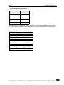
1
Technical Manual
BI-0501
MC68EN360/MC68040 based SBC
with ETHERNET, RS-232, FIELDBUS
and eight CANbus interfaces
Version 1.1
August 1997
Documentation History
Date
Version
PCB
Revision
Update
Level
Change/Description
97/03/01
1.0
1.0
-
First Release
97/08/01
1.1
1.2
-
Fault-tolerant Interface Option Added
Copyright
Copyright (c) 1997 by Brand Innovators of Digital Products bv. All rights reserved. No part of this publication may be reproduced,
transmitted, transcribed, stored in a retrieval system, or translated into any language or computer language, in any form or by any
means, electronic, mechanical, magnetic, optical, chemical, manual or otherwise, without the prior written permission of Brand
Innovators of Digital Products bv, Post Office Box 1377, 5602 BJ Eindhoven - The Netherlands.
Disclaimer
The information in this document has been carefully checked and is believed to be entirely reliable. However, no responsibility is
assumed for inaccuracies. Brand Innovators of Digital Products bv makes no representations or warranties with respect to the
contents hereof and specifically disclaims any implied warranties of merchant ability or fitness for any particular purpose. Furthermore, Brand Innovators of Digital Products bv reserves the right to make changes to any product herein to improve reliability,
function or design, without obligation of Brand Innovators of Digital Products bv to notify any person of such revision or changes.
Brand Innovators of Digital Products bv does not assume any liability arising out of applications or use of any product or circuit
described herein; neither does it convey any license under its patent rights nor the rights of others.
Table of Contents
Chapter 1
1.1
1.2
1.3
1.4
1.5
1.6
Chapter 2
2.1
2.2
2.3
2.4
Chapter 3
3.1
3.2
3.3
3.4
3.5
3.6
3.7
3.8
3.9
3.10
3.11
3.12
3.13
General Information . . . . . . . . . . . . . . . . . . . . . . . . . . . . . 1-1
Introduction. . . . . . . . . . . . . . . . . . . . . . . . . . . . . . . . . . . . . . . . . . . . .
Features . . . . . . . . . . . . . . . . . . . . . . . . . . . . . . . . . . . . . . . . . . . . . . .
General Description . . . . . . . . . . . . . . . . . . . . . . . . . . . . . . . . . . . . . .
Manual Updates . . . . . . . . . . . . . . . . . . . . . . . . . . . . . . . . . . . . . . . . .
Ordering Information . . . . . . . . . . . . . . . . . . . . . . . . . . . . . . . . . . . . .
Related Documents . . . . . . . . . . . . . . . . . . . . . . . . . . . . . . . . . . . . . .
1-1
1-1
1-2
1-2
1-2
1-3
Specifications . . . . . . . . . . . . . . . . . . . . . . . . . . . . . . . . . . 2-1
Introduction. . . . . . . . . . . . . . . . . . . . . . . . . . . . . . . . . . . . . . . . . . . . .
Components Used . . . . . . . . . . . . . . . . . . . . . . . . . . . . . . . . . . . . . . .
2.2.1 MC68EN360 . . . . . . . . . . . . . . . . . . . . . . . . . . . . . . . . . . . . .
2.2.2 MC68040. . . . . . . . . . . . . . . . . . . . . . . . . . . . . . . . . . . . . . . .
2.2.3 CAN Controllers . . . . . . . . . . . . . . . . . . . . . . . . . . . . . . . . . .
2.2.4 Memory Devices . . . . . . . . . . . . . . . . . . . . . . . . . . . . . . . . . .
2.2.5 Miscellaneous Devices . . . . . . . . . . . . . . . . . . . . . . . . . . . . .
Input/Output Options . . . . . . . . . . . . . . . . . . . . . . . . . . . . . . . . . . . . .
Specifications . . . . . . . . . . . . . . . . . . . . . . . . . . . . . . . . . . . . . . . . . . .
2-1
2-1
2-1
2-2
2-2
2-2
2-2
2-3
2-3
Installation Procedures . . . . . . . . . . . . . . . . . . . . . . . . . . 3-1
Introduction. . . . . . . . . . . . . . . . . . . . . . . . . . . . . . . . . . . . . . . . . . . . .
Installation . . . . . . . . . . . . . . . . . . . . . . . . . . . . . . . . . . . . . . . . . . . . .
Jumper Settings . . . . . . . . . . . . . . . . . . . . . . . . . . . . . . . . . . . . . . . . .
3.3.1 Slope Control. . . . . . . . . . . . . . . . . . . . . . . . . . . . . . . . . . . . .
3.3.2 Watch Dog. . . . . . . . . . . . . . . . . . . . . . . . . . . . . . . . . . . . . . .
3.3.3 Push Button Reset . . . . . . . . . . . . . . . . . . . . . . . . . . . . . . . .
Companion Mode . . . . . . . . . . . . . . . . . . . . . . . . . . . . . . . . . . . . . . . .
DRAM Placement. . . . . . . . . . . . . . . . . . . . . . . . . . . . . . . . . . . . . . . .
Battery Placement . . . . . . . . . . . . . . . . . . . . . . . . . . . . . . . . . . . . . . .
CAN Channel Connection . . . . . . . . . . . . . . . . . . . . . . . . . . . . . . . . .
Ethernet Connection . . . . . . . . . . . . . . . . . . . . . . . . . . . . . . . . . . . . .
RS-232 Connection . . . . . . . . . . . . . . . . . . . . . . . . . . . . . . . . . . . . . .
RS-485 Connection . . . . . . . . . . . . . . . . . . . . . . . . . . . . . . . . . . . . . .
Power Supply Connection . . . . . . . . . . . . . . . . . . . . . . . . . . . . . . . . .
Boundary Scan Connection . . . . . . . . . . . . . . . . . . . . . . . . . . . . . . . .
Background Debug Mode Connection . . . . . . . . . . . . . . . . . . . . . . . .
Technical Manual
i
3-1
3-1
3-1
3-1
3-2
3-2
3-2
3-3
3-3
3-3
3-4
3-4
3-4
3-4
3-4
3-4
Brand Innovators
Table of Contents (continued)
BI-0501
Chapter 4
Functional Description . . . . . . . . . . . . . . . . . . . . . . . . . . .4-1
4.1
4.2
4.3
Introduction . . . . . . . . . . . . . . . . . . . . . . . . . . . . . . . . . . . . . . . . . . . . . 4-1
68360 MPU . . . . . . . . . . . . . . . . . . . . . . . . . . . . . . . . . . . . . . . . . . . . . 4-1
68040 Companion Mode. . . . . . . . . . . . . . . . . . . . . . . . . . . . . . . . . . . 4-1
4.3.1 Differences in the Companion Mode . . . . . . . . . . . . . . . . . . . 4-1
Clock Generation . . . . . . . . . . . . . . . . . . . . . . . . . . . . . . . . . . . . . . . . 4-1
Reset Circuits . . . . . . . . . . . . . . . . . . . . . . . . . . . . . . . . . . . . . . . . . . . 4-2
4.5.1 Power Supply Monitor Reset . . . . . . . . . . . . . . . . . . . . . . . . . 4-2
4.5.2 Hardware Watchdog Circuit Reset . . . . . . . . . . . . . . . . . . . . . 4-2
4.5.3 Manual Reset . . . . . . . . . . . . . . . . . . . . . . . . . . . . . . . . . . . . . 4-2
Serial Peripheral Interface. . . . . . . . . . . . . . . . . . . . . . . . . . . . . . . . . . 4-2
Testability . . . . . . . . . . . . . . . . . . . . . . . . . . . . . . . . . . . . . . . . . . . . . . 4-3
4.7.1 JTAG Implementation. . . . . . . . . . . . . . . . . . . . . . . . . . . . . . . 4-3
4.7.2 BDM Connector . . . . . . . . . . . . . . . . . . . . . . . . . . . . . . . . . . . 4-3
CAN Interfaces . . . . . . . . . . . . . . . . . . . . . . . . . . . . . . . . . . . . . . . . . . 4-3
Interrupts. . . . . . . . . . . . . . . . . . . . . . . . . . . . . . . . . . . . . . . . . . . . . . . 4-4
4.9.1 Power Failure Interrupt . . . . . . . . . . . . . . . . . . . . . . . . . . . . . . 4-4
4.9.2 CAN Controller Interrupt . . . . . . . . . . . . . . . . . . . . . . . . . . . . 4-4
4.4
4.5
4.6
4.7
4.8
4.9
Chapter 5
Programming Considerations . . . . . . . . . . . . . . . . . . . . .5-1
5.1
5.2
Introduction . . . . . . . . . . . . . . . . . . . . . . . . . . . . . . . . . . . . . . . . . . . . . 5-1
Register Settings for 68360 Master Mode. . . . . . . . . . . . . . . . . . . . . . 5-1
5.2.1 Module Base Address Register . . . . . . . . . . . . . . . . . . . . . . . 5-1
5.2.2 Module Configuration Register. . . . . . . . . . . . . . . . . . . . . . . . 5-1
5.2.3 Auto Vector Register . . . . . . . . . . . . . . . . . . . . . . . . . . . . . . . 5-1
5.2.4 Reset Status Register . . . . . . . . . . . . . . . . . . . . . . . . . . . . . . 5-2
5.2.5 CLKO Control Register . . . . . . . . . . . . . . . . . . . . . . . . . . . . . 5-2
5.2.6 PLL Control Register . . . . . . . . . . . . . . . . . . . . . . . . . . . . . . . 5-2
5.2.7 Port E Pin Assignment Register. . . . . . . . . . . . . . . . . . . . . . . 5-2
5.2.8 System Protection Control . . . . . . . . . . . . . . . . . . . . . . . . . . . 5-2
5.2.9 Global Memory Register . . . . . . . . . . . . . . . . . . . . . . . . . . . . 5-2
5.2.10 Base Register 0 and Option Register 0 . . . . . . . . . . . . . . . . . 5-3
5.2.11 Base Register 1 and Option Register 1 . . . . . . . . . . . . . . . . . 5-3
5.2.12 Base Register 2 and Option Register 2 . . . . . . . . . . . . . . . . . 5-3
5.2.13 Base Register 3 and Option Register 3 . . . . . . . . . . . . . . . . . 5-3
5.2.14 Base Register 4 and Option Register 4 . . . . . . . . . . . . . . . . . 5-3
5.2.15 Base Register 5 and Option Register 5 . . . . . . . . . . . . . . . . . 5-4
5.2.16 Base Register 6 and Option Register 6 . . . . . . . . . . . . . . . . . 5-4
5.2.17 Base Register 7 and Option Register 7 . . . . . . . . . . . . . . . . . 5-4
5.2.18 Port A Assignments . . . . . . . . . . . . . . . . . . . . . . . . . . . . . . . . 5-4
5.2.19 Port A Open Drain Register . . . . . . . . . . . . . . . . . . . . . . . . . . 5-5
Brand Innovators
ii
Technical Manual
BI-0501
5.3
5.4
Table of Contents (continued)
5.2.20 Port A Data Register . . . . . . . . . . . . . . . . . . . . . . . . . . . . . . . 5-5
5.2.21 Port A Data Direction Register . . . . . . . . . . . . . . . . . . . . . . . 5-5
5.2.22 Port A Pin Assignment Register . . . . . . . . . . . . . . . . . . . . . . 5-5
5.2.23 Port B Assignments. . . . . . . . . . . . . . . . . . . . . . . . . . . . . . . . 5-5
5.2.24 Port B Open Drain Register. . . . . . . . . . . . . . . . . . . . . . . . . . 5-6
5.2.25 Port B Data Register . . . . . . . . . . . . . . . . . . . . . . . . . . . . . . . 5-6
5.2.26 Port B Data Direction Register . . . . . . . . . . . . . . . . . . . . . . . 5-6
5.2.27 Port B Pin Assignment Register . . . . . . . . . . . . . . . . . . . . . . 5-6
5.2.28 Port C Assignments. . . . . . . . . . . . . . . . . . . . . . . . . . . . . . . . 5-6
5.2.29 Port C Data Register . . . . . . . . . . . . . . . . . . . . . . . . . . . . . . . 5-7
5.2.30 Port C Data Direction Register . . . . . . . . . . . . . . . . . . . . . . . 5-7
5.2.31 Port C Pin Assignment Register . . . . . . . . . . . . . . . . . . . . . . 5-7
5.2.32 Port C Special Options Register . . . . . . . . . . . . . . . . . . . . . . 5-7
Register Settings for Companion Mode . . . . . . . . . . . . . . . . . . . . . . . 5-7
5.3.1 Module Base Address Register. . . . . . . . . . . . . . . . . . . . . . . 5-7
5.3.2 Module Configuration Register . . . . . . . . . . . . . . . . . . . . . . . 5-7
5.3.3 CLKO Control Register . . . . . . . . . . . . . . . . . . . . . . . . . . . . . 5-8
5.3.4 PLL Control Register . . . . . . . . . . . . . . . . . . . . . . . . . . . . . . . 5-8
5.3.5 Port E Pin Assignment Register . . . . . . . . . . . . . . . . . . . . . . 5-8
5.3.6 System Protection Control. . . . . . . . . . . . . . . . . . . . . . . . . . . 5-8
5.3.7 Global Memory Register . . . . . . . . . . . . . . . . . . . . . . . . . . . . 5-8
5.3.8 Base Register 0 and Option Register 0. . . . . . . . . . . . . . . . . 5-8
5.3.9 Base Register 1 and Option Register 1. . . . . . . . . . . . . . . . . 5-8
5.3.10 Base Register 2 and Option Register 2. . . . . . . . . . . . . . . . . 5-8
5.3.11 Base Register 3 and Option Register 3. . . . . . . . . . . . . . . . . 5-8
5.3.12 Base Register 4 and Option Register 4. . . . . . . . . . . . . . . . . 5-8
5.3.13 Base Register 5 and Option Register 5. . . . . . . . . . . . . . . . . 5-8
5.3.14 Base Register 6 and Option Register 6. . . . . . . . . . . . . . . . . 5-9
5.3.15 Base Register 7 and Option Register 7. . . . . . . . . . . . . . . . . 5-9
5.3.16 MC68EC040 . . . . . . . . . . . . . . . . . . . . . . . . . . . . . . . . . . . . . 5-9
Peripherals . . . . . . . . . . . . . . . . . . . . . . . . . . . . . . . . . . . . . . . . . . . . . 5-9
5.4.1 Flash EPROM . . . . . . . . . . . . . . . . . . . . . . . . . . . . . . . . . . . 5-10
5.4.2 DRAM . . . . . . . . . . . . . . . . . . . . . . . . . . . . . . . . . . . . . . . . . 5-10
5.4.3 SRAM . . . . . . . . . . . . . . . . . . . . . . . . . . . . . . . . . . . . . . . . . 5-10
5.4.4 CAN Ports . . . . . . . . . . . . . . . . . . . . . . . . . . . . . . . . . . . . . . 5-10
5.4.5 Board Status Register . . . . . . . . . . . . . . . . . . . . . . . . . . . . . 5-11
5.4.6 Ethernet. . . . . . . . . . . . . . . . . . . . . . . . . . . . . . . . . . . . . . . . 5-12
5.4.7 RS-232 . . . . . . . . . . . . . . . . . . . . . . . . . . . . . . . . . . . . . . . . 5-12
5.4.8 RS-485 . . . . . . . . . . . . . . . . . . . . . . . . . . . . . . . . . . . . . . . . 5-13
5.4.9 Serial EEPROM. . . . . . . . . . . . . . . . . . . . . . . . . . . . . . . . . . 5-13
5.4.10 Real Time Clock . . . . . . . . . . . . . . . . . . . . . . . . . . . . . . . . . 5-13
5.4.11 Temperature Sensor . . . . . . . . . . . . . . . . . . . . . . . . . . . . . . 5-14
5.4.12 Flex Configuration . . . . . . . . . . . . . . . . . . . . . . . . . . . . . . . . 5-14
Technical Manual
iii
Brand Innovators
Table of Contents (continued)
5.5
BI-0501
LED Indicators . . . . . . . . . . . . . . . . . . . . . . . . . . . . . . . . . . . . . . . . . 5-15
5.5.1 CAN Channel LEDs . . . . . . . . . . . . . . . . . . . . . . . . . . . . . . . 5-15
5.5.2 Ethernet status LEDs . . . . . . . . . . . . . . . . . . . . . . . . . . . . . . 5-16
5.5.3 Processor Status LED . . . . . . . . . . . . . . . . . . . . . . . . . . . . . 5-16
5.5.4 Power Indication LED. . . . . . . . . . . . . . . . . . . . . . . . . . . . . . 5-16
Appendix A
Block Diagram . . . . . . . . . . . . . . . . . . . . . . . . . . . . . . . . . . . . . . . . A-1
Appendix B
Schematic Diagrams. . . . . . . . . . . . . . . . . . . . . . . . . . . . . . . . . . . . B-1
Appendix C
Component Layout . . . . . . . . . . . . . . . . . . . . . . . . . . . . . . . . . . . . .C-1
Appendix D
List of Components. . . . . . . . . . . . . . . . . . . . . . . . . . . . . . . . . . . . .D-1
Appendix E
Connector Assignments . . . . . . . . . . . . . . . . . . . . . . . . . . . . . . . . . E-1
Appendix F
Memory Map. . . . . . . . . . . . . . . . . . . . . . . . . . . . . . . . . . . . . . . . . . F-1
Appendix G
Mechanical Specifications . . . . . . . . . . . . . . . . . . . . . . . . . . . . . . G-1
Appendix H
Application Notes . . . . . . . . . . . . . . . . . . . . . . . . . . . . . . . . . . . . . .H-1
Brand Innovators
iv
Technical Manual
List of Figures
Figure 5-1
Figure A-1
Figure C-1
Figure C-2
Figure G-1
Flex Configuration Timing . . . . . . . . . . . . . . . . . . . . . . . . . . . . . . . . 5-14
Block Diagram . . . . . . . . . . . . . . . . . . . . . . . . . . . . . . . . . . . . . . . . . . A-1
Component Layout . . . . . . . . . . . . . . . . . . . . . . . . . . . . . . . . . . . . . . . C-1
Jumper Locations . . . . . . . . . . . . . . . . . . . . . . . . . . . . . . . . . . . . . . . . C-2
Mechanical Specifications . . . . . . . . . . . . . . . . . . . . . . . . . . . . . . . . . G-1
Technical Manual
v
Brand Innovators
List of Tables
Table 1-1
Table 1-2
Table 1-3
Table 2-1
Table 3-1
Table 3-2
Table 3-3
Table 3-4
Table 3-5
Table 3-6
Table 4-1
Table 4-2
Table 4-3
Table 5-1
Table 5-2
Table 5-3
Table 5-4
Table 5-5
Table 5-6
Table 5-7
Table 5-8
Table 5-9
Table 5-10
Table 5-11
Table 5-12
Table 5-13
Table 5-14
Table 5-15
Table 5-16
Table 5-17
Table 5-18
Table D-1
Table D-2
Table D-3
Table D-4
Table D-5
Table D-6
Table D-7
Manual Updates . . . . . . . . . . . . . . . . . . . . . . . . . . . . . . . . . . . . . . . . . 1-2
Ordering Information . . . . . . . . . . . . . . . . . . . . . . . . . . . . . . . . . . . . . 1-2
List of Documents. . . . . . . . . . . . . . . . . . . . . . . . . . . . . . . . . . . . . . . . 1-3
Specifications . . . . . . . . . . . . . . . . . . . . . . . . . . . . . . . . . . . . . . . . . . . 2-3
Default Jumper Settings . . . . . . . . . . . . . . . . . . . . . . . . . . . . . . . . . . . 3-1
Slope Control Jumpers. . . . . . . . . . . . . . . . . . . . . . . . . . . . . . . . . . . . 3-2
Watch Dog Enable . . . . . . . . . . . . . . . . . . . . . . . . . . . . . . . . . . . . . . . 3-2
Push Button Reset . . . . . . . . . . . . . . . . . . . . . . . . . . . . . . . . . . . . . . . 3-2
DRAM Access Times . . . . . . . . . . . . . . . . . . . . . . . . . . . . . . . . . . . . . 3-3
DRAM Sizes . . . . . . . . . . . . . . . . . . . . . . . . . . . . . . . . . . . . . . . . . . . . 3-3
Devices on the SPI. . . . . . . . . . . . . . . . . . . . . . . . . . . . . . . . . . . . . . . 4-2
JTAG Devices . . . . . . . . . . . . . . . . . . . . . . . . . . . . . . . . . . . . . . . . . . . 4-3
External Interrupt Sources . . . . . . . . . . . . . . . . . . . . . . . . . . . . . . . . . 4-4
MC68360 Port A Usage . . . . . . . . . . . . . . . . . . . . . . . . . . . . . . . . . . . 5-4
MC68360 Port B Usage . . . . . . . . . . . . . . . . . . . . . . . . . . . . . . . . . . . 5-5
MC68360 Port C Usage . . . . . . . . . . . . . . . . . . . . . . . . . . . . . . . . . . . 5-6
Peripherals . . . . . . . . . . . . . . . . . . . . . . . . . . . . . . . . . . . . . . . . . . . . . 5-9
CAN Channel Configuration Register. . . . . . . . . . . . . . . . . . . . . . . . 5-10
Board Status Register Usage. . . . . . . . . . . . . . . . . . . . . . . . . . . . . . 5-11
CAN Channel Status . . . . . . . . . . . . . . . . . . . . . . . . . . . . . . . . . . . . 5-12
Ethernet Control Signals . . . . . . . . . . . . . . . . . . . . . . . . . . . . . . . . . 5-12
RS-232 Modem Control Signals. . . . . . . . . . . . . . . . . . . . . . . . . . . . 5-12
RS-485 Direction Control Signal . . . . . . . . . . . . . . . . . . . . . . . . . . . 5-13
Serial EEPROM Control Signals . . . . . . . . . . . . . . . . . . . . . . . . . . . 5-13
Real Time Clock Control Signals . . . . . . . . . . . . . . . . . . . . . . . . . . . 5-13
Temperature Sensor Control Signals . . . . . . . . . . . . . . . . . . . . . . . . 5-14
Flex Configuration Timing . . . . . . . . . . . . . . . . . . . . . . . . . . . . . . . . 5-15
Flex Configuration Control Signals . . . . . . . . . . . . . . . . . . . . . . . . . . 5-15
CAN Channel LEDs . . . . . . . . . . . . . . . . . . . . . . . . . . . . . . . . . . . . . 5-15
Ethernet LED Indicators . . . . . . . . . . . . . . . . . . . . . . . . . . . . . . . . . . 5-16
Processor Status . . . . . . . . . . . . . . . . . . . . . . . . . . . . . . . . . . . . . . . 5-16
List of Capacitors . . . . . . . . . . . . . . . . . . . . . . . . . . . . . . . . . . . . . . . . D-1
List of Resistors . . . . . . . . . . . . . . . . . . . . . . . . . . . . . . . . . . . . . . . . . D-1
List of Connectors and Jumpers. . . . . . . . . . . . . . . . . . . . . . . . . . . . . D-1
List of Integrated Circuits . . . . . . . . . . . . . . . . . . . . . . . . . . . . . . . . . . D-2
List of Discrete Semiconductors. . . . . . . . . . . . . . . . . . . . . . . . . . . . . D-3
List of Oscillators . . . . . . . . . . . . . . . . . . . . . . . . . . . . . . . . . . . . . . . . D-3
List of Miscellaneous Components. . . . . . . . . . . . . . . . . . . . . . . . . . . D-3
Technical Manual
vi
Brand Innovators
BI-0501
Table E-1
Table E-2
Table E-3
Table E-4
Table E-5
Table E-6
Table E-7
Table E-8
Table E-9
Table F-1
Table F-2
Table F-3
Table F-4
List of Tables (continued)
CAN Connector . . . . . . . . . . . . . . . . . . . . . . . . . . . . . . . . . . . . . . . . . E-1
10Base-T Connector . . . . . . . . . . . . . . . . . . . . . . . . . . . . . . . . . . . . . E-1
Thin Coax Connector . . . . . . . . . . . . . . . . . . . . . . . . . . . . . . . . . . . . . E-1
RS-232 Connector . . . . . . . . . . . . . . . . . . . . . . . . . . . . . . . . . . . . . . . E-2
RS-485 Connector . . . . . . . . . . . . . . . . . . . . . . . . . . . . . . . . . . . . . . . E-2
Power Supply Connector . . . . . . . . . . . . . . . . . . . . . . . . . . . . . . . . . . E-2
Boundary Scan Connector . . . . . . . . . . . . . . . . . . . . . . . . . . . . . . . . . E-2
Background Debug Mode Connector . . . . . . . . . . . . . . . . . . . . . . . . . E-3
DRAM SIMM-72 Pinning . . . . . . . . . . . . . . . . . . . . . . . . . . . . . . . . . . E-4
Cycle Types and Responding Devices. . . . . . . . . . . . . . . . . . . . . . . . F-1
Chip Select Assignments . . . . . . . . . . . . . . . . . . . . . . . . . . . . . . . . . . F-1
Addresses of CAN Channels . . . . . . . . . . . . . . . . . . . . . . . . . . . . . . . F-2
Memory Map of Each CAN Channel . . . . . . . . . . . . . . . . . . . . . . . . . F-2
Technical Manual
vii
Brand Innovators
List of Tables (continued)
Brand Innovators
BI-0501
viii
Technical Manual
Chapter 1
1.1
General Information
Introduction
This manual provides general information, preparation for use and installation instructions, operating
instructions, functional description, and support information for the BI-0501. The manual also includes
basic information needed by software engineers to design and implement software for the module.
1.2
Features
The features of the BI-0501 module include:
Local Processor
• MC68360 microprocessor with 32 bit address, 32 bit data, master or slave, 33 MHz
• MC68040 microprocessor with 32 bit address, 32 bit data, master, 33 MHz
Ethernet Compatible
• 10Base-T full duplex operation or Thin Coax using MC68160
CAN Compatible
• Eight independent CAN interface channels using Philips SJA1000 CAN controllers
• ISO/DIS 11898 high speed physical interface with optical isolation
• Fault-tolerant physical interface option
Local Memory
•
•
•
•
2 MByte Flash Memory, 32 bit wide
512 kByte SRAM with battery backup, 32 bit wide
32 Mbyte DRAM, 36 bit wide (data and parity) SIMM socket
512 byte Serial EEPROM
I/O Ports
• RS-232 asynchronous serial port
• RS-485 FieldBus port
Miscellaneous Functions
• Power monitor and watchdog
• Digital thermometer
• Alarm real time clock
Technical Manual
Page 1-1
Brand Innovators
General Information
1.3
BI-0501
General Description
The BI-0501 provides flexible and powerful connections to multiple CAN buses. The module contains
eight separate CAN network interface connections, each having its own controller and accompanying
physical network interface.
The CAN controllers are capable of handling all CAN functions on-chip. The physical interface is conform the ISO/DIS 11898 standard using the PCA82C251 CAN transceiver. A fault-tolerant physical
interface is available using the PCA82C252 CAN transceiver. To provide additional protection, the interface is optically isolated using on-board optocouplers and DC/DC converters.
The BI-0501 supports an extensive set of software options. These include both driver-level CAN functions as well as standard higher protocol software layers.
1.4
Manual Updates
Table 1-1
Manual Updates
Revision
Changes
Additions
Deletions
1.0
1.1
1.5
The fault-tolerant CAN
interface option was
added, using the
PCA82C252 CAN transceiver
Ordering Information
The next table gives an overview of the different options that are available for the BI-0501.
Table 1-2
Ordering Information
Function
Options
Microprocessor Option
MC68360
MC68040
Amount of Flash Memory
512 kByte
2 MByte
Amount of DRAM Memory
16
32
Number of CAN Channels
4
8
CAN Physical Interface
Standard
Fault-tolerant
CAN Interface Power Source
DC/DC Converters
CAN Bus power
Brand Innovators
Page 1-2
Technical Manual
BI-0501
1.6
General Information
Related Documents
The following documentation can be referred to for detailed information about related items not
described in this manual.
Table 1-3 List
of Documents
Document Title
Published by
MC68360 32-Bit Microprocessor Data Sheet
Motorola
MC68040 32-Bit Microprocessor Data Sheet
Motorola
MC68160 Enhanced Ethernet Transceiver
Motorola
SJA1000 Stand-alone CAN Controller Data Sheet
Philips Semiconductors
PDF File
mc68160rev1.pd
f
PCA82C251 24V CAN Transceiver Data Sheet
Philips Semiconductors
PCA82C252 Fault-tolerant CAN Transceiver Data Sheet
Philips Semiconductors
PCA82C252.pdf
Am29F040 Sector Erase Flash Memory Data Sheet
Advanced Micro Devices
am29f040.pdf
Am7204 High Density First-In First-Out Memory Data Sheet
Advanced Micro Devices
idt7206.pdf
DS1210 Nonvolatile Controller Chip Data Sheet
Dallas Semiconductors
ds1210.pdf
DS1232 Micromonitor Chip Data Sheet
Dallas Semiconductors
ds1232.pdf
DS1305 Serial Alarm Real Time Clock Data Sheet
Dallas Semiconductors
ds1305.pdf
DS1620 Digital Thermometer Data Sheet
Dallas Semiconductors
1620.pdf
AT25040 SPI Serial CMOS EEPROM Data Sheet
Atmel
at25040.pdf
TL7702 Supply Voltage Supervisor Data Sheet
Texas Instruments
tl7702b.pdf
FLEX 8000 Programmable Logic Device Family Data Sheet
Altera
MAX 7000 Programmable Logic Device Family Data Sheet
Altera
MT24D836 8M x 36 DRAM Module
Micron
Technical Manual
Page 1-3
dram module
Micron 36.pdf
Brand Innovators
General Information
Brand Innovators
BI-0501
Page 1-4
Technical Manual
Chapter 2
2.1
Specifications
Introduction
The BI-0501 is equipped with the SJA1000 CAN Controllers from Philips. The optical isolated physical
interfaces are based on the PCA82C251 and the PCA82C252 CAN transceivers.
2.2
Components Used
The following section gives an overview of the main parts that are used.
2.2.1
MC68EN360
The MC68EN360 QUad Integrated Communication Controller (QUICC™) is a versatile one chip integrated microprocessor and peripheral combination that can be used in a variety of controller applications. It particularly excels in communications activities. The QUICC (pronounced “quick”) can be
described as a next-generation MC68302 with higher performance in all areas of device operation,
increased flexibility, major extensions in capability, and higher integration. The term “quad” comes from
the fact there are four serial communication controllers (SCCs) on the device; however, there are actually seven serial channels: four SCCs, two serial management controllers (SMCs), and one serial
peripheral interface (SPI).
The QUICC key features are:
•
•
•
•
•
•
•
•
•
•
•
•
CPU32+ Processor
32-Bit Data Bus
32-Bit Address Bus
Memory Controller supports DRAM, SRAM, EPROM, Flash EPROM.
Four general purpose timers
Two independent DMAs
Software Watchdog
RISC Communications Processor Module
Baud rate generators
Ethernet controller
UARTs
SPI controller
The QUICC supports a slave mode to disable the internal CPU32+ which allows use with an external
processor. The MC68040 Companion Mode allows the QUICC to be an MC68040 Companion Chip
and intelligent peripheral. All the QUICC features are usable in the slave mode.
Technical Manual
Page 2-1
Brand Innovators
Specifications
2.2.2
BI-0501
MC68040
The MC68040 is Motorola’s third generation of M68000-compatible, high performance, 32-bit microprocessors. The MC68040 is a virtual memory microprocessor employing multiple concurrent execution
units and a highly integrated architecture that provides very high performance in a monolithic HCMOS
device. The processor integrates an MC68030-compatible integer unit and two independent caches. It
also contains dual, independent, demand-page memory management units (MMUs) for instruction and
data stream accesses and independent, 4-KByte instruction and data caches. The MC68040 contains
an MC68882-compatible floating-point unit (FPU). The use of multiple independent execution pipelines,
multiple internal buses, and a full internal Harvard architecture, including separate physical caches for
both instruction and data accesses, achieves a high degree of instruction execution parallelism.
2.2.3
CAN Controllers
The SJA1000 is a highly integrated stand-alone controller for the Controller Area Network (CAN) used
within automotive and general industrial environments. It contains all the necessary features required to
implement a high performance communication protocol. The programmable transfer rate of the
SJA1000 goes up to 1 MBaud. The SJA1000 can operate in the BasicCAN (PCA82C200 compatible)
and the PeliCAN (CAN 2.0B compatible) mode.
The PCA82C251 is the standard interface between the CAN protocol controller and the physical bus. It
is intended for high speed applications up to 1 MBaud and is fully compatible with the ISO/DIS 11898
standard. The fault-tolerant option using the PCA82C252 transceiver is intended for low-speed applications with baud rates up to 125 kBaud. This option supports one-wire transmission in the event of bus
failure.
2.2.4
Memory Devices
The Flash memory consists of four 1-MBit or 4-MBit Flash type EPROMs, giving a 32-bit wide, 512
kByte or 2 MByte non-volatile execution memory. The Am29F040 is a 4 Mbit, 5.0 Volt-only Flash memory organized as 512 Kbyte of 8 bits each. This device can be programmed in-system with the standard
system 5.0 V Vcc supply. This device also features a sector erase architecture. the sector mode allows
for 64K byte blocks of memory to be erased and reprogrammed without effecting other blocks.
The SRAM memory consists of four 1-MBit type SRAMs, giving a 32-bit wide, 512 kByte data memory.
The added DS1210 Nonvolatile Controller Chip converts the CMOS SRAM into nonvolatile memory.
The DRAM memory is located in a industry standard 72-pin SIMM socket giving 32-bit wide, 32 MByte
of general purpose memory.
The 512 bytes serial E2PROM AT25040 is Serial Peripheral Interface (SPI) compatible and features a
Write Disable instruction for software data protection.
2.2.5
Miscellaneous Devices
The DS1620 Digital Thermometer provides 9-bit temperature readings which indicate the temperature
of the device. User defined temperature settings are stored in nonvolatile memory. Temperature settings and readings are all communicated to and from the DS1620 over a 3-wire interface.
The DS1305 Serial Alarm Real Time Clock provides a full BCD clock calendar which is accessible via
the SPI compatible serial interface. Two programmable time of day alarms are provided by the DS1305.
Brand Innovators
Page 2-2
Technical Manual
BI-0501
Specifications
Each alarm can generate an interrupt on a programmable combination of seconds, minutes, hours, and
day.
2.3
Input/Output Options
CAN Options
•
•
•
•
Eight independent CAN channels
ISO/DIS 11898 compatible isolated physical interface
Fault-tolerant option
Front panel LED for each channel
Ethernet Options
•
•
•
•
10Base-T
Thin Coax
Selects automatically the active interface
Isolated physical interfaces
Serial Interface Options
• Asynchronous RS-232 with isolated physical interface
• Fieldbus port RS-485 with isolated physical interface
Miscellaneous
• Front panel LED for MPU Status and Power Status
• Power connector accepts from 9 to 36 Vdc @ 36 W Maximum
2.4
Specifications
The BI-0501 specifications are given in the next table.
Table 2-1 Specifications
Characteristics
Specifications
Power requirements
9 to 36 Vdc @ 36 W (maximum)
Operating temperature
0 to 70 degrees C ambient air temperature
Storage temperature
-25 to 85 degrees C
Relative humidity
5% to 90% (non-condensing)
Dimensions
Width
366.7 mm (14.437 inches)
Depth
160 mm (6.299 inches)
Thickness
35.6 mm (1.402 inches)
Technical Manual
Page 2-3
Brand Innovators
Specifications
Brand Innovators
BI-0501
Page 2-4
Technical Manual
Installation Procedures
Chapter 3
3.1
Introduction
This chapter provides the preparation and installation instructions for the BI-0501.
3.2
Installation
The module is shipped in an antistatic container to protect the module against static electricity. When
the module is unpacked, avoid touching areas of integrated circuitry to prevent static discharge from
damaging the circuits.
Jumpers are used to select hardware specific options. The jumper block positioning and default jumper
settings are illustrated in Appendix C.
3.3
Jumper Settings
The next table gives a summary of the available jumpers, their default settings and their functions.
Table 3-1 Default
Jumper Settings
Description
Jumper
Block
Default Setting
Status
Section
Slope Control
JBxx
2-3 Connected
Normal mode
3.3.1
Watch Dog
JB17
1-2 Connected
Watchdog is enabled
3.3.2
Push Button Reset
JB52
1-2 Not Connected
Reset is not active
3.3.3
3.3.1
Slope Control
When using the standard CAN physical interface, the slope control mode allows the use of an
unshielded twisted pair as bus lines. To reduce RFI, the rise and fall slope should be limited. The rise
and fall slope is programmed using a 47 kOhm resistor when the jumper is in Slope Control mode.
When the jumper is in Normal Mode, no slope control is active and the interface can be operated using
its highest speeds.
Technical Manual
Page 3-1
Brand Innovators
Installation Procedures
BI-0501
A seperate jumper is available to select the operation mode of each standard CAN transceiver. Note
that, when using the fault-tolerant transceivers, the slope control jumpers are not available.
Table 3-2
Slope Control Jumpers
CAN
Channel
Jumper
Slope Control
Normal Mode
(default)
1
JB21
1-2
2-3
2
JB22
1-2
2-3
3
JB14
1-2
2-3
4
JB15
1-2
2-3
5
JB19
1-2
2-3
6
JB20
1-2
2-3
7
JB18
1-2
2-3
8
JB16
1-2
2-3
3.3.2
Watch Dog
The watchdog timer is default set to reset the microprocessor when the watchdog strobe input is not
driven low prior to the 1.2 second time-out. The watchdog can be disabled by connecting the strobe
input to a continuously active clock.
Table 3-3
Watch Dog Enable
Jumper
Position
Description
JB17
1-2
Strobe input is connected to
Red Status LED output of the 68360 (default)
2-3
Strobe input is connected to
continuously running clock (watchdog is disabled)
3.3.3
Push Button Reset
The push-button jumper can be connected to a external switch to reset the microprocessor. The processor will be reset when the switch is closed. The push-button input is debounced and an active reset
pulse of 250 ms minimum is guaranteed.
Table 3-4
Push Button Reset
Jumper
Position
Description
JB52
1-2
Reset the microprocessor of the BI-0501
3.4
Companion Mode
The BI-0501 can be operated in the companion mode when a MC68040 is inserted into the provided
socket. No further changes to the hardware are necessary.
Brand Innovators
Page 3-2
Technical Manual
BI-0501
3.5
Installation Procedures
DRAM Placement
The status of the four Presence Detect signals PRD[3:0] from the SIMM are available in the Board Status Register. The DRAM controller parameters of the QUICC must be set according to the DRAM module’s size and access time. The available combinations of the presence detect signals are described in
the next tables.
Table 3-5 DRAM
Access Times
Presence Detect Code PRD[3:0]
Access Time in ns
00xx
100
01xx
80
10xx
70
11xx
60
The sizes in MByte given in between the () are for smaller SIMMs which were using the same size
codes.
Table 3-6 DRAM
Sizes
Presence Detect Code PRD[3:0]
Size in MByte
Control Signals
xx00
4
RAS1
xx01
32 (2)
RAS1, RAS2
xx10
16 (1)
RAS1
xx11
8
RAS1, RAS2
3.6
Battery Placement
There should always be a battery inserted in the battery holder of the BI-0501. The real time clock
depends on it to keep its time valid and the SRAM to keep its data valid during power down periods.
When replacing the battery special care must be taken to use the proper orientation of the plus and the
minus of the battery. Use only Lithium 3.6 Volts, Size AA batteries which will give a battery backup time
of at least 15 years. To preserve battery power, when inserting a battery in a power down period, the
real time clock and SRAM devices will not receive power from the battery until a power up and power
down has been detected.
3.7
CAN Channel Connection
The CAN physical interface can either take its power from the Bus Power as supplied from the CAN
connector or it can use the power from the DC/DC converter. When using the Bus Power option, be
aware that proper behaviour of the physical interface can only be achieved when this Bus Power is actually present. For signal pin assignment, signal direction and connector type, see Table E-1, “CAN Connector” on page E-1.
Technical Manual
Page 3-3
Brand Innovators
Installation Procedures
3.8
BI-0501
Ethernet Connection
The ethernet controller can either use the Twisted Pair or the Thin Coax connection. In the Auto Port
Selection mode, the controller selects the Twisted Pair or Coax port depending on the presence of valid
link beats or frames at the Twisted Pair receive pins. This means that when both Twisted Pair and Coax
is available to the BI-0501, it will give a higher priority to the Twisted Pair port. When the controller is not
in the Auto Port Selection mode, then the Twisted Pair Port Enable signal from the QUICC determines
which port will be selected.
3.9
RS-232 Connection
The BI-0501 provides, in addition to the send and transmit data signals, the control and handshake signals needed to operate standard external modems. For signal pin assignment, signal direction and connector type, see Table E-4, “RS-232 Connector” on page E-2.
3.10
RS-485 Connection
The RS-485 data signals are implemented as bidirectional transceivers. Therefore, a RS-485 direction
signal is available from the QUICC to the RS-485 drivers. For signal pin assignment, signal direction
and connector type, see Table E-5, “RS-485 Connector” on page E-2.
3.11
Power Supply Connection
The BI-0501 requires a single, 9 to 36 Vdc @ 36 W maximum, power supply for operation. The BI-0501
has a 4 A electronic fuse on the power supply, and it is protected against reverse connection of the
power supply. For signal pin assignment, signal direction and connector type, see Table E-6, “Power
Supply Connector” on page E-2.
3.12
Boundary Scan Connection
All Boundary Scan Test (BST) signals have pull-up resistors connected. For signal pin assignment, signal direction and connector type, see Table E-7, “Boundary Scan Connector” on page E-2.
3.13
Background Debug Mode Connection
When the BI-0501 is used in the 68360 mode, the Background Debug Mode (BDM) interface can be
used to manage the 68360. A standard Personal Computer (PC) may be connected to the BI-0501’s
BDM port using a BDM interface box which is attached to the PC’s standard parallel port. This setup
makes it possible to down load and debug software on the BI-0501.
Brand Innovators
Page 3-4
Technical Manual
BI-0501
Installation Procedures
Note that the BDM port is not available when the BI-0501 is used in the 68040 Companion mode. For
signal pin assignment, signal direction and connector type, see Table E-8, “Background Debug Mode
Connector” on page E-3.
Technical Manual
Page 3-5
Brand Innovators
Installation Procedures
Brand Innovators
BI-0501
Page 3-6
Technical Manual
Chapter 4
4.1
Functional Description
Introduction
This chapter gives an overview of the BI-0501 module and a detailed description of the functional sections. The block diagram of the module is given in Appendix A and the schematic diagrams are given in
Appendix B.
4.2
68360 MPU
The 68360 is the main processor on the BI-0501.
4.3
68040 Companion Mode
The BI-0501 can be used with or without the 68040 installed. The BI-0501 detects that an 68040 is
plugged into the socket and makes all necessary changes to the hardware automatically. Therefore
there are no jumpers to be replaced when switching from 68360 to 68040 mode.
4.3.1
Differences in the Companion Mode
•
•
The Boundary Scan path are rerouted to include the 68040 device.
•
•
Burst memory accesses are enabled to the memory devices.
The 68030 is notified during power up reset that the companion mode is entered and that the internal CPU of the 68360 must be disabled.
The BDM functionality is not longer available.
4.4
Clock Generation
In the BI-0501’s design all devices that need clock signals are provided with their own clock source.
This approach makes it easier to change certain clock frequencies in a later stadium of the BI-0501
product life, without affecting other, non related, parts of the design.
In the 68360 master mode and the 68040 companion mode, a single 32 MHz clock oscillator is used.
This implies that low power modes can not be achieved by turning down the clock frequency. A single
16 MHz clock oscillator is used for all eight CAN channels and the accompanying FLEX device. The
Real Time Clock uses a 32.768 crystal. The Ethernet physical interface uses a 20 MHz oscillator.
Technical Manual
Page 4-1
Brand Innovators
Functional Description
4.5
BI-0501
Reset Circuits
The BI-0501 supports a variety of reset sources.
The DS1232 MicroMonitor Chip monitors three vital conditions: power supply, software execution and
external override.
4.5.1
Power Supply Monitor Reset
The DS1232 MicroMonitor Chip monitors the power supply value and will assert reset when the supply
drops below 4.75 Vdc. The reset outputs of the DS1232 are also used for the power status indicator
LED. When the power supply falls below 4.75 volts, the processor is stopped by asserting the reset
input. On power up, reset is kept active for a minimum of 250 ms to allow the power supply and processor to stabilize.
4.5.2
Hardware Watchdog Circuit Reset
The watchdog timer of the DS1232 must be stimulated on the ST input or it will reset the processor. The
watchdog must be kicked every 1.2 seconds. When the hardware watchdog must be disabled, it can be
connected to a continuous clock signal using the jumper. The watchdog is triggered using the output
signal from the general I/O pin to the red processor status LED.
4.5.3
Manual Reset
A jumper header is provided to reset the processor. This header can be connected to a separate external reset button when needed.
4.6
Serial Peripheral Interface
Serial Peripheral Interface (SPI) is a full-duplex, synchronous, character-orientated channel that supports a four-wire interface (receive, transmit, clock and slave select).
SPICLK is the clock output, SPIMISO is the receiver input, SPIMOSI is the transmitter output. SPISEL
is not used as the SPI select to the 68360 and can be used as a general purpose I/O. Make sure to disable the SPISEL input in the master SPI mode.
Table 4-1
Devices on the SPI
Device
Device Name
Real Time Clock
DS1305
Serial EEPROM
AT25040
Brand Innovators
Page 4-2
Technical Manual
BI-0501
4.7
Functional Description
Testability
The BI-0501 contains many Surface Mounted Devices (SMD). Therefore Boundary Scan Test (BST)
methodology has been implemented to make production testing possible. This methodology is also
used to program the In-System Programmable (ISP) logic and the Flash Memory.
4.7.1
JTAG Implementation
The following table gives the Boundary Scan Test chain.
Table 4-2 JTAG
Devices
Device
Device Name
TRST
TDI Net Name
TDO Net Name
Microcontroller
MC68360
Yes
TDI
TDO_to_040
Companion Microcontroller
MC68040
Yes
TDI_to_040
TDO_from_040
Companion Mode Glue Logic
EPM7032
No
TDO_from_040
TDI_to_CAN
CAN Interface FPGA
EPF8820
Yes
TDI_to_CAN
TDI_to_FIFO
FIFO Buffer
ABT8652
No
TDI_to_FIFO
TDO_from_FLEX
Board Status Register
(Presence Detect and FLEX)
ABT8652
No
TDO_from_FLEX
TDI_to_SUPPLY
Board Status Register
(CAN Status)
ABT8652
No
TDI_to_SUPPLY
TDO_from_SUPPLY
Board Status Register
(CAN LEDs 5 to 8)
ABT8652
No
TDO_from_SUPPLY
TDO_between_LEDS
Board Status Register
(CAN LEDs 1 to 4)
ABT8652
No
TDO_between_LEDS
TDO
4.7.2
BDM Connector
The BDM connector is connected to the BDM interface signals of the 68360 microcontroller. When
using these signals, total control can be taken over the microcontroller for debug, test and verification of
the BI-0501’s hardware and software. The BDM connector can also be used for the initial loading of the
FLASH memory devices.
4.8
CAN Interfaces
The CAN supply monitoring circuit checks whether the transceiver section (the isolated section) has a
power supply available. This is an indication whether the bus power supply from the CAN connector is
present.
Technical Manual
Page 4-3
Brand Innovators
Functional Description
4.9
BI-0501
Interrupts
The BI-0501 provides several internal and external interrupt sources. The internal interrupt sources are
fully described in the 68360 users manual. The external interrupt sources are given in the following
table.
Table 4-3
External Interrupt Sources
Interrupt Input
Usage
IRQ7
-
IRQ6
Iout[2] in companion mode, not available as interrupt input
IRQ5
Power Failure Interrupt
IRQ4
Iout[1] in companion mode, not available as interrupt input
IRQ3
CAN Controller Interrupt
IRQ2
-
IRQ1
Iout[0] in companion mode, not available as interrupt input
PORTC 11
-
PORTC 10
-
PORTC 9
Data Carrier Detect RS232
PORTC 8
Clear to Send RS232
PORTC 7
Ring Indicator RS232
PORTC 6
-
PORTC 5
-
PORTC 4
-
PORTC 3
-
PORTC 2
-
PORTC 1
Temperature Interrupt
PORTC 0
Real Time Clock Interrupt
4.9.1
Power Failure Interrupt
The power supply input voltage is continuously monitored. The active low Power Failure interrupt input
will be activated when the power supply input voltage drops below 11 Vdc. This early warning will give
the microprocessor at least 5 milliseconds before the 5 Vdc will drop and the microprocessor is reset. In
this time period it can save its register contents into battery backed up SRAM.
4.9.2
CAN Controller Interrupt
This active low interrupt input will be active when at least one of the CAN controllers has its interrupt
output active.
Brand Innovators
Page 4-4
Technical Manual
Chapter 5
5.1
Programming
Considerations
Introduction
This section contains all necessary information for programmers to take full advantage of the features
of the BI-0501 module. The descriptions will include implementation dependent information that cannot
be found in the respective data sheets.
This chapter should be used in conjunction with the references given in “Related Documents” on page
1-3. System programmers are expected to be fully conversant with all the material and have the relevant experience before writing their own system software.
Appendix F shows the Memory map and the I/O map of the BI-0501 module.
5.2
Register Settings for 68360 Master Mode
The QUICC internal registers must be programmed after hardware reset as described in the following
paragraphs. The addresses and programming values are in hexadecimal base.
Please refer to the MC68360 QUICC User’s Manual for more information.
The following register settings are used in 68360 master mode. The register settings used in companion mode are found in the section “Register Settings for Companion Mode” on page 5-7.
5.2.1
Module Base Address Register
The QUICC’s module base address register (MBAR) controls the location of its internal memory and
registers and their access space. The QUICC MBAR resides at a fixed location in 0x0003FF00 in the
CPU space. The MBAR must be initialized to 0xFFFFE001 to obtain the memory map as described in
Table F-2, “Chip Select Assignments” on page F-1.
5.2.2
Module Configuration Register
The MCR controls the SIM60 configuration in the QUICC. The BSTM bit in the MCR must be set to
zero. This setting will enable using asynchronous timing on the bus signals.
5.2.3
Auto Vector Register
The auto vector register (AVR) contains 8 bits that correspond to external interrupt levels that require an
auto vector response. The AVR must be initialized to 0x28 to generate auto vectors for interrupt levels 5
and 3.
Technical Manual
Page 5-1
Brand Innovators
Programming Considerations
5.2.4
BI-0501
Reset Status Register
The reset status register (RSR) indicates the source of the last reset that occurred, when the relevant
bit is set. This register must be cleared after every reset, so that when the next reset occurs, its source
can be easily determined. The register is cleared by writing 0xFF.
5.2.5
CLKO Control Register
The CLKO control register (CLKOCR) controls the operation of the CLKO(0:1) pins. This register must
be initialized to 0x0E. This enables CLKO1 with 1/3 strength to the EPM7032 and disables the CLKO2
to the 68040.
5.2.6
PLL Control Register
The PLL control register (PLLCR) controls the operation of the PLL. There is no need to program the
PLLCR after hard reset, because the configuration of the MODCK(0:1) pins on the BI-0501 determines
its value. It is recommended to set the PLLWR bit to prevent accidental writing.
5.2.7
Port E Pin Assignment Register
Port E pins can be programmed by the port E pin assignment register (PEPAR). The A(31:28) pins of
the master QUICC can be programmed as address lines or as write enable W(0:3) lines. Bit 7 in the
PEPAR must be cleared to select address lines function, and it must be set to select the write enable
function. Until this bit is written, the A(31:28) pins are three-stated.
Port E pins can be programmed by the port E pin assignment register (PEPAR). The PEPAR must be
initialized to 0x07C0 to configure Port E of the QUICC as follows:
•
•
•
•
•
RAS1 and RAS2 double drive function is used to drive the DRAM.
The A(31:28) pins of the QUICC are configured as write enable lines.
The OE/AMUX pin is configured as AMUX to drive the external multiplexers of the DRAM.
The CAS(0:3) output function is used for the DRAM.
CS7 output function is enabled.
5.2.8
System Protection Control
The system protection register (SYPCR) controls the system monitors, the software watchdog, and the
bus monitor timing. This register must be initialized to 0x3C to disable the software watchdog, and to
enable the bus monitor function.
5.2.9
Global Memory Register
The global memory register (GMR) contains selections for the memory controller of the QUICC. The
GMR must be initialized according to the size and the access time of the DRAM SIMM installed on the
BI-0501. This register is initialized with 0x1FE00100.
The GMR defines the following parameters:
• The DRAM refresh period is 15.52 millisecond.
Brand Innovators
Page 5-2
Technical Manual
BI-0501
Programming Considerations
31 + 1RFCNT + 1 - = --------------Refresh Period = ----------------------------------= 15.515152
33 ⁄ 16
System clk ⁄ 16
(EQ 1)
• The DRAM refresh cycle length depends on the DRAM access time
and it is either 3 clocks or 4 clocks long.
•
•
•
•
The DRAM module port size is 32 bits.
The parity is enabled.
The CS/RAS lines of the QUICC will not assert when accessing the CPU space.
Internal address multiplexer for the DRAM is disabled.
5.2.10
Base Register 0 and Option Register 0
Base register 0 (BR0) and Option register 0 (OR0) control the operation of CS0 pin of the master
QUICC. The Flash Memory of the BI-0501 is connected to this pin. BR0 must be initialized to
0x00000051, and OR0 must be initialized to 0xFFE00000 to obtain the memory map as described in
Table F-2, “Chip Select Assignments” on page F-1.
5.2.11
Base Register 1 and Option Register 1
Base register 1 (BR1) and Option register 1 (OR1) control the operation of RAS1 pin of the QUICC.
This pin is connected to the DRAM module. These registers must be initialized according to the type of
the DRAM SIMM installed on the BI-0501.
BR1 must be initialized to 0x01000051, disregarding the type and the access time of the DRAM.
The software must perform 8 accesses to the RAS1 address space after initialization for proper operation of the DRAM.
5.2.12
Base Register 2 and Option Register 2
Base register 2 (BR2) and Option register 2 (OR2) control the operation of RAS2 pin of the QUICC.
This pin is connected to the DRAM module. These registers must be initialized when the type of the
DRAM SIMM installed on the BI-0501 contains two DRAM banks.
The software must perform 8 accesses to the RAS2 address space after initialization for proper operation of the DRAM.
5.2.13
Base Register 3 and Option Register 3
Base register 3 (BR3) and Option register 3 (OR3) control the operation of CS3 pin of the QUICC. The
SRAM on the BI-0501 is connected to this pin. BR3 must be initialized to 0x03000051, and OR3 must
be initialized to 0xFFF80000 to obtain the memory map as described in Table F-2, “Chip Select Assignments” on page F-1.
5.2.14
Base Register 4 and Option Register 4
Base register 4 (BR4) and Option register 4 (OR4) control the operation of CS4 pin of the QUICC. The
CAN Controllers are connected to this pin. BR4 must be initialized to 0x04000051, and OR4 must be
Technical Manual
Page 5-3
Brand Innovators
Programming Considerations
BI-0501
initialized to 0xFFFF8006 to obtain the memory map as described in Table F-2, “Chip Select Assignments” on page F-1.
5.2.15
Base Register 5 and Option Register 5
Base register 5 (BR5) and Option register 5 (OR5) control the operation of CS5 pin of the QUICC. CS7
is not used on the BI-0501.
5.2.16
Base Register 6 and Option Register 6
Base register 6 (BR6) and Option register 6 (OR6) control the operation of CS6 pin of the QUICC. The
Board Status Register is connected to this pin. BR6 must be initialized to 0x06000051, and OR6 must
be initialized to 0xFFFFF800 to obtain the memory map as described in Table F-2, “Chip Select Assignments” on page F-1.
5.2.17
Base Register 7 and Option Register 7
Base register 7 (BR7) and Option register 7 (OR7) control the operation of CS7 pin of the QUICC. CS7
is not used on the BI-0501.
5.2.18
Port A Assignments
Pins in boldface have open drain capability.
Table 5-1
MC68360 Port A Usage
Pin name
Pin Function
Direction
Board Function
A0
RXD1
In
Receive Data Ethernet
A1
TXD1
Out
Transmit Data Ethernet
A2
RXD2
A3
TXD2
A4
RXD3
In
Receive Data RS232
A5
TXD3
Out
Transmit Data RS232
A6
RXD4
In
Receive Data RS485
-
A7
TXD4
Out
Transmit Data RS485
A8
CLK1
In
Receive Clock Ethernet
A9
CLK2
In
Transmit Clock Ethernet
A10
CLK3/TIN2
-
A11
General Purpose IO
Out
Diagnostic Loopback
A12
General Purpose IO
In/Out
Twisted Pair Port Enable
A13
General Purpose IO
Out
Auto Port Select
A14
General Purpose IO
Out
Twisted Pair Signal Quality Error Test Enable
A15
General Purpose IO
Brand Innovators
-
Page 5-4
Technical Manual
BI-0501
5.2.19
Programming Considerations
Port A Open Drain Register
Port A of the QUICC is 16 pins port, and each pin may be configured as general purpose I/O pin or as
dedicated peripheral interface pin. The port A open drain register (PAODR) configures the drivers of
port A pins as open-drain or as active drivers.
5.2.20
Port A Data Register
Port A data register (PADAT) can be read to check the data at the pin. If a port pin is configured as general purpose output pin, the value in the PADAT for that pin is driven onto the pin.
5.2.21
Port A Data Direction Register
The port A data direction register (PADIR) has different functions according to the configuration of the
port pins. If a pin is general purpose I/O pin, the value in the PADIR for that pin defines the direction of
the pin. If a pin is dedicated peripheral interface pin, the value in the PADIR for that pin may select one
of two dedicated functions of the pin.
5.2.22
Port A Pin Assignment Register
The port A pin assignment register (PAPAR) configures the function of the port pins. If the value in the
PAPAR for a pin is zero the pin is general purpose I/O, otherwise the pin is dedicated peripheral interface pin.
5.2.23
Port B Assignments
Pins in boldface have open drain capability.
Table 5-2 MC68360
Port B Usage
Pin name
Pin Function
Direction
Board Function
B0
General Purpose IO
Out
AT25040 Chip select (SPI)
B1
SPICLK
Out
RTC / AT25040 Serial Data Clock
B2
SPIMOSI
Out
RTC / AT25040 Serial Data In
B3
SPIMISO
In
RTC / AT25040 Serial Data Out
B4
General Purpose IO
Out
Real Time Clock Chip Select (SPI)
B5
General Purpose IO
In/Out
Temperature Data (open collector) + FLEX data
B6
General Purpose IO
Out
Temperature Clock + FLEX Clock
B7
General Purpose IO
Out
Temperature RST
B8
General Purpose IO
Out
Twisted Pair Full Duplex Mode Select
B9
General Purpose IO
Out
CONFIG to FLEX
B10
General Purpose IO
In
Low battery Warning
B11
General Purpose IO
Out
Data Terminal Ready RS232
B12
RTS1
Out
Transmit Enable Ethernet
B13
RTS2
In
Data Set Ready RS232
B14
RTS3
Out
Request To Send RS232
B15
RTS4
Out
Direction RS485
Technical Manual
Page 5-5
Brand Innovators
Programming Considerations
Table 5-2
BI-0501
MC68360 Port B Usage
Pin name
Pin Function
Direction
Board Function
B16
General Purpose IO
Out
Processor Status Green + Watchdog Trigger
B17
General Purpose IO
Out
Processor Status Red
5.2.24
Port B Open Drain Register
Port B of the QUICC is 18 pins port, and each pin may be configured as general purpose I/O pin or as
dedicated peripheral interface pin. The port B open drain register (PBODR) configures the drivers of
port B pins as open-drain or as active drivers.
5.2.25
Port B Data Register
Port B data register (PBDAT) can be read to check the data at the pin. If a port pin is configured as general purpose output pin, the value in the PBDAT for that pin is driven onto the pin.
5.2.26
Port B Data Direction Register
The port B data direction register (PBDIR) has different functions according to the configuration of the
port pins. If a pin is general purpose I/O pin, the value in the PBDIR for that pin defines the direction of
the pin. If a pin is dedicated peripheral interface pin, the value in the PBDIR for that pin may select one
of two dedicated functions of the pin.
5.2.27
Port B Pin Assignment Register
The port B pin assignment register (PBPAR) configures the function of the port pins. If the value in the
PBPAR for a pin is zero the pin is general purpose I/O, otherwise the pin is dedicated peripheral interface pin.
5.2.28
Port C Assignments
All Port C pins have interrupt capability.
Table 5-3
MC68360 Port C Usage
Pin name
Pin Function
Direction
Board Function
C0
General Purpose IO
In
Real Time Clock Interrupt
C1
General Purpose IO
In
Temperature Interrupt
C2
RTS3
C3
RTS4
C4
CTS1
In
Collision Ethernet
C5
CD1
In
Receive Enable Ethernet
C6
CTS2
C7
CD2
In
Ring Indicator RS232
C8
CTS3
In
Clear to Send RS232
C9
CD3
In
Data Carrier Detect RS232
Brand Innovators
-
-
Page 5-6
Technical Manual
BI-0501
Programming Considerations
Table 5-3 MC68360
Port C Usage
Pin name
Pin Function
C10
CTS4
-
C11
CD4
-
5.2.29
Direction
Board Function
Port C Data Register
Port C of the QUICC is 12 pin port, and each pin may be configured as general purpose I/O pin or as
dedicated peripheral interface pin, with interrupt capability. Port C data register (PCDAT) can be read to
check the data at the pin. If a port pin is configured as general purpose output pin, the value in the
PCDAT for that pin is driven onto the pin.
5.2.30
Port C Data Direction Register
The port C data direction register (PCDIR) has different functions according to the configuration of the
port pins. If a pin is general purpose I/O pin, the value in the PCDIR for that pin defines the direction of
the pin. If a pin is dedicated peripheral interface pin, the value in the PCDIR for that pin may select one
of three dedicated functions of the pin.
5.2.31
Port C Pin Assignment Register
The port C pin assignment register (PCPAR) configures the function of the port pins, along with PCDIR
and PCSO.
5.2.32
Port C Special Options Register
The port C special options register (PCSO) configures the CDx and CTSx pins. Port C can detect
changes on the CTS and CD lines, and assert the corresponding interrupt while the SCC simultaneously uses those lines.
5.3
Register Settings for Companion Mode
The QUICC internal registers must be programmed after hardware reset as described in the following
paragraphs. The addresses and programming values are in hexadecimal base.
Please refer to the MC68360 QUICC User’s Manual for more information.
5.3.1
Module Base Address Register
See “Module Base Address Register” on page 5-1.
5.3.2
Module Configuration Register
See “Module Configuration Register” on page 5-1.
Technical Manual
Page 5-7
Brand Innovators
Programming Considerations
5.3.3
BI-0501
CLKO Control Register
The CLKO control register (CLKOCR) controls the operation of the CLKO(1:2) pins. This register must
be initialized to 0x06 after reset to enable CLKO2 and CLKO1.
5.3.4
PLL Control Register
See “PLL Control Register” on page 5-2.
5.3.5
Port E Pin Assignment Register
See “Port E Pin Assignment Register” on page 5-2.
5.3.6
System Protection Control
See “System Protection Control” on page 5-2.
5.3.7
Global Memory Register
See “Global Memory Register” on page 5-2.
5.3.8
Base Register 0 and Option Register 0
See “Base Register 0 and Option Register 0” on page 5-3.
5.3.9
Base Register 1 and Option Register 1
See “Base Register 1 and Option Register 1” on page 5-3.
5.3.10
Base Register 2 and Option Register 2
See “Base Register 2 and Option Register 2” on page 5-3.
5.3.11
Base Register 3 and Option Register 3
See “Base Register 3 and Option Register 3” on page 5-3.
5.3.12
Base Register 4 and Option Register 4
See “Base Register 4 and Option Register 4” on page 5-3.
5.3.13
Base Register 5 and Option Register 5
See “Base Register 5 and Option Register 5” on page 5-4.
Brand Innovators
Page 5-8
Technical Manual
BI-0501
5.3.14
Programming Considerations
Base Register 6 and Option Register 6
See “Base Register 6 and Option Register 6” on page 5-4.
5.3.15
Base Register 7 and Option Register 7
See “Base Register 7 and Option Register 7” on page 5-4.
5.3.16
MC68EC040
When using the MC68360 in companion mode with an MC68EC040 the cache on the MC68EC040 can
slow down the serial channel performance of the system. The MC68040 does not have this problem
because it can use it’s MMU to specify memory cache behavior on a page by page basis.
To alleviate the cache problem with the MC68EC040 a trick can be used: reduce the system’s memory
space to 1GB by not using address line A31 and A30. This has the added “benefit” that now the four
1GB address ranges overlap. By reprogramming the MC68EC040’s access control registers it becomes
possible to specify for each 1GB address range what the caching behavior should be. Note that this
scheme relies entirely on software: if one would access data using an inappropriate 1GB address range
it would still be cached (or not, depending on your wishes).
Because the A31 and A30 address lines are not used for anything else, this scheme allows the use of
an MC68EC040 on the BI-0501.
5.4
Peripherals
The following peripherals are available on the BI-0501:
Table 5-4 Peripherals
Name
Access
Flash EPROM
CS0
DRAM
CS1
DRAM
CS2
SRAM
CS3
CAN Ports
CS4
comment
CS5
Board Status Register
not used
CS6
CS7
not used
Ethernet
Internal serial port
RS-232
Internal serial port
RS-485
Internal serial port
Serial EEPROM
SPI
4-wire serial port
Real Time Clock
SPI
4-wire serial port
Temperature Sensor
Port pins
3-wire serial port
Flex Configuration
Port pins
5-wire serial port
Technical Manual
Page 5-9
Brand Innovators
Programming Considerations
5.4.1
BI-0501
Flash EPROM
Four devices of 1MBit or 4MBit are installed giving either 512 kByte or 2 MByte of FLASH EEPROM.
The FLASH devices can be programmed from a single 5 volt supply. When four Am29F040 devices are
installed, 8 equal size sectors of 256 kByte (4 devices times 64 kByte) can be erased independently.
While the devices are in programming/erase mode it is not possible to read from the device (page 15 of
Am29040 data sheet, DQ7, DQ6, DQ5 and DQ3 description). It is feasible to transfer all needed information during programming/erasing to SRAM and or DRAM. Note that DRAM may not always be available and that SRAM is limited to 512 kByte. Also be aware that programming/erasing one sector inhibits
reads from all other sectors also.
5.4.2
DRAM
A SIMM socket is available for DRAM SIMM72 devices with capacities up to 8 MByte x 32 (or 36 with
parity) giving 32 MByte of DRAM.
DRAM Access Times signals are routed to 4 inputs of the Board Status Register.
5.4.3
SRAM
Four devices of 1MBit each are used in an 32 bit data width. This gives 512 kByte of SRAM.
The DS1210 is used as battery back up for the SRAM devices and the Real Time Clock DS1302. The
tolerance pin of the DS1210 is connected to Vcco so power fail is detected in the range of 4.50 to 4.25
volts. The TL7702BI senses the battery voltage and asserts the LOWBAT signal to the ‘360 when the
battery voltage drops below 2.53 Volts (Typical).
Two circuits monitor the power supply voltage (the watchdog and the SRAM battery circuit), the reset
circuit is active first, then the SRAM will be disabled.
5.4.4
CAN Ports
Each CAN channel is build using three building blocks:
1.
A CAN controller with its physical interface.
2.
A First-In-First-Out (FIFO) memory device.
3.
A FPGA that connects the CAN controller to the FIFO and the 68360 microcontroller.
The CAN controller is accessible by the 68360 at the addresses as described in Table F-4, “Memory
Map of Each CAN Channel” on page F-2. Two additional addresses are defined to access the FIFO and
the CAN Channel Configuration Register, which is internal to the FPGA.
Table 5-5
CAN Channel Configuration Register
7
6
5
4
3
2
1
0
Interrupt Active
-
-
-
DMA Enable
FIFO Empty
FIFO Half Full
Controller Interrupt Active
• Interrupt Active: When this read-only bit is set, at least one of the CAN controllers has its interrupt
active.
Brand Innovators
Page 5-10
Technical Manual
BI-0501
Programming Considerations
• DMA Enable: This read/write bit enables the DMA Controller of the FPGA to respond to receive
interrupts from the CAN controller. When this bit is set, the microcontroller should read
the received CAN messages from the FIFO device. When this bit is cleared, the microcontroller should read received CAN messages from the receive buffer of the CAN controller.
• FIFO Empty: When this read-only bit is set, the FIFO device is empty.
• FIFO Half Full: When this read-only bit is set, the FIFO device is half full.
• Controller Interrupt Active: When this read-only bit is set, this CAN controller has its interrupt active.
5.4.5
Board Status Register
The board status register is used to set and reset the CAN channel LEDs and to read back the FLEX
status and the status of the CAN channels.
The board status register can be written and read back. Note that all bits are always written, so updating this register should always be a read-modify-write sequence. All written bits can be read back. The
bits are used as follows:
Table 5-6 Board
Status Register Usage
Bit Number
Write
Read
Comment
31-30
LED for channel 8
Written Value
See CAN Channel LEDs
29-28
LED for channel 7
Written Value
See CAN Channel LEDs
27-26
LED for channel 6
Written Value
See CAN Channel LEDs
25-24
LED for channel 5
Written Value
See CAN Channel LEDs
23-22
LED for channel 4
Written Value
See CAN Channel LEDs
21-20
LED for channel 3
Written Value
See CAN Channel LEDs
19-18
LED for channel 2
Written Value
See CAN Channel LEDs
17-16
LED for channel 1
Written Value
See CAN Channel LEDs
15 - 14
-
Not used
Reads always one
13
-
STATUS from FLEX
A zero means that configuration was unsuccessful
12
-
CONFIG_DONE from FLEX
A one means that FLEX is
configured properly
11
-
PRD4 from DRAM
See DRAM Access Times
10
-
PRD3 from DRAM
See DRAM Access Times
9
-
PRD2 from DRAM
See DRAM Access Times
8
-
PRD1 from DRAM
See DRAM Access Times
7
-
Status CAN channel 8
See CAN Channel Status
6
-
Status CAN channel 7
See CAN Channel Status
5
-
Status CAN channel 6
See CAN Channel Status
4
-
Status CAN channel 5
See CAN Channel Status
3
-
Status CAN channel 4
See CAN Channel Status
2
-
Status CAN channel 3
See CAN Channel Status
1
-
Status CAN channel 2
See CAN Channel Status
0
-
Status CAN channel 1
See CAN Channel Status
Technical Manual
Page 5-11
Brand Innovators
Programming Considerations
BI-0501
The LED registers are initialized to ‘1’s during reset.
The CAN status bits have different meaning when different options for the physical interfaces are chosen.
Table 5-7
CAN Channel Status
Physical Interface
Option
Power
Option
Signal source
Status is ‘0’
Status is ‘1’
Standard
Power from bus
Bus power
Bus power is present
Bus power is absent
Standard
Power from system
Fault-tolerant
5.4.6
Jumper
Channel is present
Channel is absent
Error from transceiver
Error is active
Error is not active
Ethernet
Although most of the functionality of the ethernet interface is managed by the communication processor
of the 68360, some ethernet options can be set with the following bits.
Table 5-8
Ethernet Control Signals
Name
Direction
Port Bit
High
Low
Diagnostic Loopback
Out
PA11
Loopback mode
Normal operation
Twisted Pair Port Enable
In/Out
See Auto Port Select
PA12
Twisted Pair Port selected
Thin Coax Port selected
Auto Port Select
Out
PA13
Auto Port Select Mode
Twisted Pair Port Enable
is an input
Manual Port Select Mode
Twisted Pair Port Enable
is an output
Twisted Pair Signal Quality
Error Test Enable
Out
PA14
Disabled
Enabled
Twisted Pair Full Duplex
Mode Select
Out
PB8
Full Duplex disabled
Full Duplex enabled
5.4.7
RS-232
The RS232 port has modem control lines which must be handled separately.
Table 5-9
RS-232 Modem Control Signals
Name
Direction
Port Bit
Data Carrier Detect
In
PC9
Data Set Ready
In
PB13
Ring Indicator
In
PC7
Data Terminal Ready
Out
PB11
Brand Innovators
Page 5-12
Technical Manual
BI-0501
5.4.8
Programming Considerations
RS-485
The RS-485 port has a separate direction signal.
Table 5-10 RS-485
Direction Control Signal
Name
Direction
Port Bit
High
Low
Direction
Out
PB15
Driver to RS-485 bus enabled
Driver to RS-485 bus disabled
5.4.9
Serial EEPROM
The AT25040 is a SPI compatible CMOS serial E2PROM. It can contain 4k (512 x 8) bit of information
and provides write protection in software.
The SPI manager of the 68360 is used in the master mode providing clock and enable signals. The
SPIMISO pin is then an input and is connected to the AT25040 serial data out pin.
Table 5-11 Serial
EEPROM Control Signals
Name
Direction
CE
Out
PB0
Select the Serial EEPROM
SDI
Out
PB2
Data to Serial EEPROM
SDO
In
PB3
Data from Serial EEPROM
SCLK
Out
PB1
Clock to the Serial EEPROM
5.4.10
Port Bit
Usage
Real Time Clock
The DS1305 RTC has an SPI interface and two additional interrupt outputs (open drain with external
pull-up). The SPI will speed up the rate that the real time can be updated what can be an advantage
when time stamping is needed for incoming CAN messages. The SPI is combined with the EEPROM
SPI interface signals.
Table 5-12 Real
Time Clock Control Signals
Name
Direction
Port Bit
Usage
CE
Out
PB4
Select the Real Time Clock
SDI
Out
PB2
Data to Real Time Clock
SDO
In
PB3
Data from Real Time Clock
SCLK
Out
PB1
Clock to the Real Time Clock
INT0/1
In
PC0
Interrupt output from the Real Time Clock
Technical Manual
Page 5-13
Brand Innovators
Programming Considerations
5.4.11
BI-0501
Temperature Sensor
The Dallas DS1620 uses a three wire data transmission protocol. The RST and CLK inputs are connected to general purpose outputs, the DQ input/output pin of the DS1620 is connected to a three-state
port pin and has a pull-up resistor.
Table 5-13
Temperature Sensor Control Signals
Name
Direction
Port Bit
Usage
RST
Out
PB7
Reset the Temperature Sensor
DQ
In/Out
PB5
Data to and from the Temperature Sensor
CLK
Out
PB6
Clock to the Temperature Sensor
TCOM
In
PC1
Interrupt output from the Temperature Sensor
The DS1620 has a temperature range of -55 to +125 degrees C in steps of 0.5 degrees C (9 bit value).
The Tcom signal (TTL output) is connected to a port C input. Port C inputs can generate interrupts on
any change (low-to-high or high-to-low). The Tcom output changes when either Tlow or Thigh is
exceeded. This gives an amount of hysteresis.
5.4.12
Flex Configuration
The Flex device is a SRAM based FPGA, which will loose its configuration during power down periods.
After power up or when the Flex configuration needs to be updated during operation of the BI-0501, the
in-circuit reconfiguration has to be executed.
tCFG
nCONFIG
tCF2ST
tSTATUS
nSTATUS
tCF2CD
CONF_DONE
tCF2CK
tCH
tCL
tDSU
DCLK
DATA
D0
D1
Figure 5-1 Flex
Brand Innovators
D2
D3
D4
tDH
D5
Configuration Timing
Page 5-14
Technical Manual
BI-0501
Programming Considerations
Table 5-14 Flex
Configuration Timing
Symbol
Parameter
Maximum
Unit
tCF2CD
nCONFIG low to CONF_DONE low
1
µs
tCF2ST
nCONFIG low to nSTATUS low
1
µs
tCFG
nCONFIG low pulse width
2
µs
tSTATUS
nSTATUS low pulse width
2.5
µs
tCF2CK
nCONFIG high to first rising edge on DCLK
5
µs
tDSU
Data setup time before rising edge on DCLK
50
ns
tDH
Data hold time after rising edge on DCLK
0
ns
tCH
DCLK high time
80
ns
tCL
DCLK low time
80
ns
tCLK
DCLK period
160
ns
fMAX
DCLK maximum frequency
Table 5-15 Flex
Minimum
6
MHz
Configuration Control Signals
Name
Direction
Port Bit
Usage
DCLK
Out
PB6
A Low-to-High clocks data in to the Flex device
DATA
In/Out
PB5
Configuration data to the Flex
nCONFIG
Out
PB9
A Low-to-High will restart configuration of the Flex
5.5
LED Indicators
A variety of indicator LEDs are available on the BI-0501.
5.5.1
CAN Channel LEDs
Per CAN channel a bicolour LED is available. Each LED can be activated by writing two bits in the
Board Status Register.
Table 5-16 CAN
LED
Channel LEDs
Value
off
“00”
green
“10”
red
“01”
orange
“11“
Technical Manual
Page 5-15
Brand Innovators
Programming Considerations
5.5.2
BI-0501
Ethernet status LEDs
The ethernet interface has four LED indicators.
Table 5-17
Ethernet LED Indicators
Name
Colour
Meaning
Link Pass
Green
The interface indicates a good link integrity on
the twisted pair port
Transmit
Red
The interface is transmitting data
Receive
Red
The interface is receiving data
Collision
Red
The interface detects a collision or jabber condition
5.5.3
Processor Status LED
This is a bicolour LED for the processor status. The green LED is connected to general purpose I/O pin
B16 with pull-up of the 68360 using an inverter-driver. After reset this pin will tri-state and the green
LED will be turned off. The green LED will be lit when a zero is written to B16. The RED led is connected via two inverter-drivers (the output of the first inverter goes to watch-dog circuit) to general purpose I/O pin B17 with pull-up to be sure that the red LED will be lit when a reset occurs. The red LED
will be lit when a one is written to B17.
Table 5-18
Processor Status
LED
Value B17-B16
off
“01“
red
“11“
green
“00“
orange
“10“
5.5.4
Power Indication LED
A bicolour LED to verify whether 5Vdc is available. The green LED is connected to the high active
RESET output of the power monitor DS1232, the red LED to the low active RESETN output of the
DS1232. When power is applied the red LED will be active until the reset time-out of 250ms is passed.
Then the green LED will be on. When power supply is below 4.75 V the red LED will be on.
Brand Innovators
Page 5-16
Technical Manual
Appendix A
Block Diagram
Figure A-1 Block
Technical Manual
Diagram
Appendix A-1
Brand Innovators
Block Diagram
Brand Innovators
BI-0501
Appendix A-2
Technical Manual
Appendix B
Schematic Diagrams
1.
Top Schematics
2.
MC68EN360 Microcontroller
3.
MC68040 Microcontroller
4.
Various Functions
5.
68360 Microcontroller
6.
68040 Microcontroller
7.
512KB SRAM
8.
512K-2MByte FLASH Memory
9.
DRAM Controller
10.
CAN Interfaces
11.
Board Status Registers
12.
Board Status Registers
13.
CAN Interface FPGA
14.
CAN Channels 1 to 4
15.
CAN Channels 5 to 8
16.
Fifo Data buffer
17.
Fifo Can Controller #1
18.
Fifo Can Controller #2
19.
Fifo Can Controller #3
20.
Fifo Can Controller #4
21.
Fifo Can Controller #5
22.
Fifo Can Controller #6
23.
Fifo Can Controller #7
24.
Fifo Can Controller #8
25.
Ethernet Interface
26.
RS-232 Interface
27.
RS-485/Profibus Interface
28.
Boudary Scan Interface
29.
Power Supply and Decoupling
30.
Miscellaneous
Technical Manual
Appendix B-1
Brand Innovators
Schematic Diagrams
Brand Innovators
BI-0501
Appendix B-2
Technical Manual
Appendix C
Component Layout
Figure C-1 Component
Technical Manual
Appendix C-1
Layout
Brand Innovators
Component Layout
BI-0501
Figure C-2 Jumper
Brand Innovators
Locations
Appendix C-2
Technical Manual
List of Components
Appendix D
Table D-1 List
of Capacitors
Quantity
Reference Designator
Device
Value
76
C1-24, C27-68, C87, C90-91, C95-96, C98-100, C110-111
VP41BY104KBT
0.1UF
1
C25
222268358391
390PF
3
C26, C92, C94
222262919103
0.01UF
8
C69-76
222262919102
1000PF
10
C77-84, C93, C101
222237111105
1UF
2
C85-86
222202114103
10000UF
1
C88
CK05BX393K
0.039UF
1
C89
CK05BX392K
3900PF
2
C112-113
222212255109
10UF
Table D-2 List
of Resistors
Quantity
Reference Designator
Device
Value
2
R1-2
232218143562
5K6
8
R3-10
232215621005
1M
2
R11-12
232218143272
2K7
1
R13
232215621201
120
25
R14-16, R25-28, R41, R45-61
232218143392
3K9
8
R17-24
232218143473
47K
4
R29-32
232218143152
1K5
1
R33
232215621002
1K_1%
1
R34
232218143105
1M
8
R35-37, R42-43, R69-71
232215623909
39
1
R38
232215622941
294
2
R39-40
232215624999
50
8
R44, R62-68
232218190018
0
16
RN1-16
4610X-101-392
3K9
6
RNS1-6
4608X-102-271
270
Table D-3 List
of Connectors and Jumpers
Quantity
Reference Designator
Device
1
J1
1-0227161-3
4
J2-3, J6, J9
9-0215593-1
Technical Manual
Appendix D-1
Brand Innovators
List of Components
Table D-3
BI-0501
List of Connectors and Jumpers
Quantity
Reference Designator
Device
1
J4
SS6488SAFLS
1
J5
1-0106505-2
6
J7-8, J10-11, J13-14
0-0216926-1
9
JB1, JB14-16, JB18-22
SIP-3P
1
JB2-3
TSF-24DS-0000
7
JB9-13, JB17, JB53
HEADER10
4
JB23-26
SIP\2P
1
JB52
SIP-2P
Table D-4
List of Integrated Circuits
Quantity
Reference Designator
Device
1
U1
MC68EN360FE33
1
U2
MC68040RC33
3
U3-5
74F157
1
U6
DS1210
1
U7
AT25040-10PC
1
U8
EPF8820AQC-4
1
U9
DS1620S
35
U10, U12-15, U17, U19-43, U60, U117-119
HCPL-7101
5
U11, U73, U75-76, U91
SN74ABT8652DL
1
U16
DS1232
1
U18
EPM7032LC44-15
10
U44-45, U109-116
LT1121CZ-5
10
U46-50, U53-55, U121-122
DCP010505
1
U51
2VP5U9
1
U52
MC68160BFB
8
U56, U58-59, U61-65
PCA82C251T
1
U57
74F04
8
U66-72, U74
AM7204A-50-JC
8
U77-79, U81, U83-84, U90, U92
UA78M05C
1
U80
DP8392CV
1
U82
DS1305
4
U85-88
AM29F040-90-JC
1
U89
SN75176BP
8
U93, U95, U100-105
SJA1000T
4
U94, U96-98
TC551001AFL
1
U99
SIMM72
1
U106
4N46
1
U107
EC6E01
Brand Innovators
Appendix D-2
Technical Manual
BI-0501
List of Components
Table D-4 List
of Integrated Circuits
Quantity
Reference Designator
Device
1
U108
TL7702BIP
1
U120
LT1137ACG
8
U123-130
PCA82C252T
Table D-5 List
of Discrete Semiconductors
Quantity
Reference Designator
Device
Value
1
CR1
1N916
1
CR2
PBYR1645
17
CR3, CR5-20
1N5819
1
CR4
1N4738A
8.2V
1
VAR1
5SS410MBKCA
0.01UF/2KV
8
VAR2-9
RIE103SAQCF0K
0.01UF/500V
Table D-6 List
of Oscillators
Quantity
Reference Designator
Device
Value
1
X1
X356H
20MHZ
1
X2
1
X3
X360H
32MHz
1
X4
X355H
16Mhz
Table D-7 List
32.768KHz
of Miscellaneous Components
Quantity
Reference Designator
Device
Value
1
B1
CELLHOLDER
3.6V
1
MF1
MF-R400-PTC
4A
1
T1
FL1012/1066
1
T2
LT6032
Technical Manual
Appendix D-3
Brand Innovators
List of Components
Brand Innovators
BI-0501
Appendix D-4
Technical Manual
Connector Assignments
Appendix E
In this appendix the pinning is given of the CAN Connector, the 10Base-T Connector, the Thin Coax
Connector, the RS-485 Connector, the RS-232 Connector and the Power Supply Connector.
The CAN connector is a 9 pin, male D type connector. This is the CAN interface port of the QUICC.
Table E-1 CAN
Connector
Pin number
Name
Direction
1
-
-
2
CAN_L
In/Out
3
Ground
-
4
-
-
5
Bus Shield
-
6
Ground
-
7
CAN_H
In/Out
8
-
-
9
Bus Power
In
The 10Base-T connector is a 8 pin, RJ-45 connector. This is the twisted-pair Ethernet port of the
QUICC.
Table E-2 10Base-T
Connector
Pin number
Name
Direction
1
TD+
Out
2
TD-
Out
3
RD+
In
4
-
-
5
-
-
6
RD-
In
7
-
-
8
-
-
The Thin Coax connector is a coax connector. It is the Thin Coax Ethernet port of the QUICC.
Table E-3 Thin
Coax Connector
Pin number
Name
1
TXO/RXI
In/Out
2
Ground (Shield)
-
Technical Manual
Direction
Appendix E-1
Brand Innovators
Connector Assignments
BI-0501
The RS-232 connector is a 9 pin, male D type connector. It is the RS-232 serial port of the QUICC.
Table E-4 RS-232
Connector
Pin number
Name
Direction
JB8 Pins
1
Data Carrier Detect
In
1
2
Receive Data
In
3
3
Transmit Data
Out
5
4
Data Terminal Ready
Out
7
5
Signal Ground
-
9
6
Data Set Ready
In
2
7
Request to Send
Out
4
8
Clear to Send
In
6
9
Ring Indicator
In
8
The RS-485 connector is a 9 pin, female D type connector. It is the RS-485 serial port of the QUICC.
Table E-5 RS-485
Connector
Pin number
Name
Direction
1
-
-
2
-
-
3
Data Negative
In/Out
4
-
-
5
Signal Ground
-
6
+5 Vdc
Out
7
-
-
8
Data Positive
In/Out
9
-
-
The Power Supply connector is a 3 pin connector. It is the Power Supply connector for the QUICC.
Table E-6 Power
Supply Connector
Pin Number
Pin Name
Description
Specification
1
Power
Power supply to all devices
9 - 36 Vdc, 36 Watts
2
Ground
Power return path
3
Shield
Shielding protection
The Boundary Scan connector is a double-row, 10 pin, male connector. It provides access to the
Boundary Scan signals of the BI-0501 for testing and programming purposes.
Table E-7 Boundary
Scan Connector
Pin Number
Name
Description
1
TRST
Test Reset
2
Ground
3
TDO
Brand Innovators
Test Data Out
Appendix E-2
Technical Manual
BI-0501
Connector Assignments
Table E-7 Boundary
Scan Connector
Pin Number
Name
4
Ground
5
TDI
6
Ground
7
TMS
8
Ground
9
TCK
10
Ground
Description
Test Data In
Test Mode Select
Test Clock
The BDM connector is a double-row, 10 pin, male connector. It provides the BDM signals of the QUICC,
so that it can be controlled by an external BDM controller. Note that the BDM mode is not supported in
the 68040 companion mode.
Table E-8 Background
Debug Mode Connector
Pin number
Description
68360 Signal
1
Data Strobe
DS
2
Bus Error
BERR
3
Ground
4
DSCLK
5
Ground
6
FREEZE
FREEZE
7
Microcontroller Reset
MPURST
8
DSI
IFETCH
9
+5 Vdc
10
DSO
Technical Manual
BKPT
IPIPE0
Appendix E-3
Brand Innovators
Connector Assignments
BI-0501
The following table gives the connection of the SIMM pins to the board signals.
Table E-9 DRAM
SIMM-72 Pinning
Pin number
Name
Pin number
Name
Pin number
Name
Pin number
Name
1
GND
21
D20
41
CAS2
61
D13
2
D0
22
D5
42
CAS3
62
D30
3
D16
23
D21
43
CAS1
63
D14
4
D1
24
D6
44
RAS0
64
D31
5
D17
25
D22
45
RAS1
65
D15
6
D2
26
D7
46
NC
66
NC
7
D18
27
D23
47
WE
67
PRD1
8
D3
28
MA7
48
NC
68
PRD2
9
D19
29
NC
49
D8
69
PRD3
10
VCC
30
VCC
50
D24
70
PRD4
11
NC
31
MA8
51
D9
71
NC
12
MA0
32
MA9
52
D25
72
GND
13
MA1
33
RAS3
53
D10
14
MA2
34
RAS2
54
D26
15
MA3
35
Parity1
55
D11
16
MA4
36
Parity3
56
D27
17
MA5
37
Parity2
57
D12
18
MA6
38
Parity0
58
D28
19
MA10
39
GND
59
VCC
20
D4
40
CAS0
60
D29
Brand Innovators
Appendix E-4
Technical Manual
Memory Map
Appendix F
Table F-1 Cycle
Types and Responding Devices
FC3 - FC0
Address Space
Responding Devices
0000
Reserved
None
0001
User Data
All
0010
User Program
All
0011
Reserved
None
0100
Reserved
None
0101
Supervisor Data
All
0110
Supervisor Program
All
0111
Supervisor CPU
MBAR registers in QUICC device and
QUICC during interrupt acknowledge cycle
1000
DMA
All
The following table gives the preferred address map for the BI-0501 chip select setup. Note that this
preferred map is in no way dictated by the hardware and therefore a different address map may be
selected. The upper two address bits should be zero, as described in “MC68EC040” on page 9.
Table F-2 Chip
Select Assignments
Chip
Select
Accessed
Device
Start
Address
End
Address
Data
Size
CS0
2M Flash EPROM
0x00000000
0x001FFFFF
32
CS1
16M DRAM
0x01000000
0x01FFFFFF
32
CS2
16M DRAM
0x02000000
0x02FFFFFF
32
CS3
512K SRAM
0x03000000
0x0307FFFF
32
CS4
CAN 0 to 7
0x04000000
0x04007FFF
8
CS5
-
-
-
CS6
Board Status Register
0x06000000
0x060007FF
CS7
-
-
-
-
QUICC Internal Memory
0xFFFFE000
0xFFFFFFFF
Technical Manual
Appendix F-1
32
32
Brand Innovators
Memory Map
BI-0501
The eight CAN controllers occupy addresses that are 0x1000 apart.
Table F-3 Addresses
of CAN Channels
Channel
Start Address
End Address
0
0x04000000
0x04000FFF
1
0x04001000
0x04001FFF
2
0x04002000
0x04002FFF
3
0x04003000
0x04003FFF
4
0x04004000
0x04004FFF
5
0x04005000
0x04005FFF
6
0x04006000
0x04006FFF
7
0x04007000
0x04007FFF
The memory map of each CAN channel is identical. All registers are internal to the CAN controller
except for the last two registers.
Table F-4 Memory
Map of Each CAN Channel
Address Offset
Name
Direction
0x003
CAN Controller Address 0
Read/
Write
:
:
:
:
:
:
:
:
:
0x07F
CAN Controller Address 31
Read/
Write
0x100
Fifo Data
Read Only
0x113
Channel Configuration
Read/
Write
Brand Innovators
Appendix F-2
Technical Manual
Appendix G
Mechanical Specifications
Figure G-1 Mechanical
Technical Manual
Specifications
Appendix G-1
Brand Innovators
Mechanical Specifications
Brand Innovators
BI-0501
Appendix G-2
Technical Manual
Appendix H
Technical Manual
Application Notes
Appendix H-1
Brand Innovators
Application Notes
Brand Innovators
BI-0501
Appendix H-2
Technical Manual