1
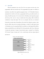
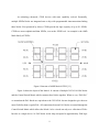
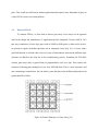
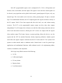
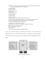
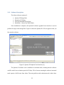
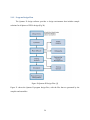
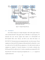
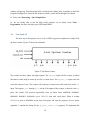
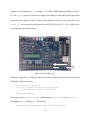
Investigation of Altera DE2 Development and Education Board
COP 4902 Independent Study
Joseph Voelmle
1/20/2009
1 INTRODUCTION TO FPGAS ................................................................................................................................. 2
1.1
BASIC THEORY .......................................................................................................................................... 2
1.2
BASICS OF PLAS ........................................................................................................................................ 5
1.3
OTHER FPDS ............................................................................................................................................. 8
1.4
BASICS OF FPGAS ................................................................................................................................... 10
2 DEVELOPMENT WITH THE ALTERA DE2 EVALUATION BOARD .......................................................................... 19
2.1
H/W AND S/W CONFIGURATION............................................................................................................ 19
2.1.1
HARDWARE DESCRIPTION ...................................................................................................................... 19
2.1.2
SOFTWARE DESCRIPTION ....................................................................................................................... 22
2.1.3
PROGRAM DESIGN FLOW ....................................................................................................................... 24
2.2
CASE STUDY #1 ....................................................................................................................................... 25
2.3
STEPS TO COMPILE AND UPLOAD HELLO_WORLD TO THE BOARD ......................................................... 29
2.4
CASE STUDY #2 ....................................................................................................................................... 30
3 CONCLUSION .................................................................................................................................................... 34
REFERENCES......................................................................................................................................................... 36
APPENDIX 1 ......................................................................................................................................................... 37
APPENDIX 2 ......................................................................................................................................................... 40
APPENDIX 3 ......................................................................................................................................................... 41
APPENDIX 4 ......................................................................................................................................................... 42
1
1 Introduction to FPGAs
We begin by providing some background on programmable logic and the reasons
for the popularity of Field Programmable Devices (FPD). There are many different types of
devices and architectures the designer will encounter, and one should be familiar with the
different terminology used in the field. There are a wide variety of FPDs that the designer can
choose. In addition to FPDs, Programmable Logic Devices (PLDs) is another name that the
designer will encounter for FPDs. FPD is a general term while PLDs historically refer to
relatively simple devices. A Programmable Logic Array (PLA) is relatively small FPD
consisting of two levels of logic, an AND plane followed by an OR plane, with both levels being
programmable. A Programmable Array Logic (PAL) is also a relatively small FPD with a
programmable AND plane followed by a fixed OR plane. (PAL is trademarked by Advanced
Micro Devices.) Simple PLD (SPLD) is usually a PLA or a PAL. A Complex PLD (CPLD)
consists of multiple SPLD-like blocks on a chip. A Field Programmable Gate Array (FPGA) is a
FPD consisting of a very general structure allowing a very high density.
1.1
Basic Theory
Combinational digital circuits are based on Boolean algebra. A common form of Boolean
equations is known as canonical, two-level, product-of-sums. Here, a function can be expressed
by ANDing terms together (first level) and ORing these together (second level) to form an
2
output. The advantage of this is that these functions can be readily realized by using AND gates
followed by OR gates. For example, a function
F = AB’C’ + A’B + BC
could be implemented by:
Figure 1 Circuit implementing formula F = AB’C’ + A’B + BC [14]
The individual products terms, AB’C’, A’B, and BC, are known as minterms. For simple
designs, this technology is sufficient, but it was found that more complex designs required other
techniques.
Early digital circuits were designed using discrete logic such as 7400 series of transistortransistor logic (TTL) integrated circuits. This series includes not only devices containing logic
gates, such as the 7400 which contains four NAND gates, but also more complex devices such as
flip-flops, counters, decoders, and multiplexers. Unlike older technologies, which relied on many
small scale integration (SSI) chips such as the 7400 series, designs today consist mainly of highdensity devices. The first use of user programmable logic was realized by Programmable ReadOnly Memory (PROM), where address lines are the inputs to the logic circuit and data read from
3
those address locations form the logic circuit output. This is a form of look-up table (LUT)
where we use the input to look up the output by indexing a table. (Fig. 2)
Figure 2 Internal Organization of a ROM [14]
As an example, Figure 3 shows a combinational logic implementation (two-level
canonical form) using a PROM with the associated Boolean equations for the outputs.
Figure 3 Combinational logic implementation using a ROM [14]
4
Using PROMs are advantageous when design time is short (there is no need to minimize
output functions), most input combinations are needed (such as for code converters), and there is
little sharing of product terms among output functions. There are however, several
disadvantages. One is that the size doubles for each additional input. Logic functions rarely
require more than a few product terms. Since a PROM has a full decoder we can’t take
advantage of don’t cares 1 and have to account for all input combinations. PROMs are an
inefficient architecture for implementing logic circuits since only a fraction of their capacity is
used in any one application. For these reasons, they are rarely used for this purpose.
1.2
Basics of PLAs
Programmable Logic Arrays (PLAs) were specifically developed for implementing
programmable logic circuits. A PLA contains a programmable AND array or plane followed by a
programmable OR plane.
Figure 4 Programmable Logic Array [14]
1
Don’t cares occur when certain input conditions will never occur or the output will not be changed by those input
conditions. This can be used to simplify functions by reducing the number of minterms.
5
In Figure 4, we can see that the general organization of a PLA is similar to that of a
PROM. Exploiting the regular structure of two level logic introduced in the previous section,
PLAs arrange the AND and OR gates into a generalized structure whose connections can be
programmed to implement a particular function. The AND array is used to compute the
particular minterm and the OR array ORs these terms together to form the final product-of-sums
output.
Figure 5 PLA connections before programming [14]
In order to program the PLA, selected connections between wires in a circuit like the one in Fig.
5, are open or closed by a programmable switch.
Suppose we wish to implement the following logic equations:
F0
F1
F2
F3
=
=
=
=
6
A + B’C’
AC’ + AB
B’C’ + AB
B’C + A
Exploiting the fact that some of the minterms are used more than once, we could program a PLA
to implement these equations as follows, as illustrated in Fig 6.
Figure 6 Example of a programmed PLA [14]
A short-hand notation for describing the topology of array logic shows connection
between wires as x’s and multiple wires entering gates as single wires, as illustrated in Fig 7.
Figure 7 Short-hand notation of a programmed PLA [14]
7
1.3
Other FPDs
When first introduced in the early 1970s, PLA were expensive and slow due to the
programmable AND arrays and OR arrays. The programmable logic planes were difficult to
manufacture and suffered from significant propagation delays. In 1978 Monolithic Memories
introduced PALs. Like PLAs, PALs have a programmable AND array, but differ from PLAs in
having a fixed OR array (Fig. 8). To overcome the lack of flexibility in not being able to program
the OR array, PALs come in a variety of standard dual in-line packages (DIP) with different
combinations of inputs and outputs. PALs were very important when they were introduced
because they overcame many of the problems of the earlier PLAs. Being less expensive, faster,
and more reliable, they proved very popular with designers. A single PLA could replace dozens
of 7400 family devices. In categorizing FPDs, PLAs and PALs are called Simple PLDs (SPLDs).
Industry standard SPLDs are the 16R8 and 22V10 PALs produced by AMD. Here, 16R8 means
16 inputs and a maximum of 8 outputs. R means that the output is “registered” by a D flip-flop.
22V10 means 22 inputs, 10 outputs, and V is for a versatile output, with some outputs registered
and some not.
Figure 8 Structure of a PAL [11]
8
As technology advanced, CPLD devices with more capability evolved. Essentially,
multiple SPLDs blocks are integrated onto a chip with programmable interconnections linking
these blocks. First pioneered by Altera, CPLDs provide the logic capacity of up to 50 SPLDs.
CPLDs are more sophisticated than SPLDs, even at the SPLD level. An example is the AMD
Mach family of CPLDs.
Figure 9 Structure of AMD Mach 4 CPLD [11]
Figure 9 shows the layout of the Mach 4. It consists of multiple 34V16 PAL-like blocks
and the Central Switch Matrix which connects these blocks together. When we say “PAL-like”
we mean that the PAL blocks are equivalent to the 34V16 PAL but are designed to give the user
more flexibility than a regular PAL. All connections between PAL blocks are routed through the
Central Switch Matrix which allows the Mach 4 to be viewed not only as a collection of PALs
but also as a single device. 16 PAL blocks on the chip correspond to approximately 5000 logic
9
gates. This is still not sufficient for modern applications that require many thousands of gates on
a chip. FPGAs seem to solve that problem.
1.4
Basics of FPGAs
To examine FPGAs, we first need to discuss gate arrays. Gate arrays are an approach
used in the design and manufacture of Application-Specific Integrated Circuits (ASICs). In a
gate array, transistors, or basic logic gates such as NAND or NOR gates, or other active devices,
are placed at regular, predefined positions on an integrated circuit (Fig. 10). A circuit with a
specified function is realized when a layer or layers of interconnects between the different logic
elements are added to the chip late in the manufacturing process. Extending the PLA/PAL
concept, gate arrays allow a general form of programmable wires on a chip. This removes the
restriction of having gates arranged in a two level AND-OR form. This is a more expensive and
time consuming to manufacture, but can achieve gates densities in the millions and speeds much
greater than PLAs/PALs.
Figure 10 General Structure of a Gate Array [14]
10
Today, most prototypes, and many production designs use Field Programmable Devices
(FPDs) and FPGAs in particular. An FPGA or field-programmable gate array is a semiconductor
device containing basic programmable logic components called "logic blocks", and wires
between those blocks. Unlike gate arrays, whose wires must be manufactured on to the chip, the
wires on FPGAs are programmable as well. FPGA logic blocks and wires can be programmed in
the field (hence the name) very rapidly which makes it the premier technology for prototyping.
Logic blocks can be programmed to perform the function of basic logic gates such as AND, and
XOR, or more complex combinational functions such as decoders or mathematical functions. In
most FPGAs, the logic blocks also include memory elements, which may be simple flip-flops or
more complete blocks of memory. 1, 2 FPGAs combine the density advantages of gate arrays with
the programmability of PALs/PLAs. The advantages of FPGAs are low start-up costs, a shorter
time to market, lower non-recurring engineering costs, instant manufacturing turnaround, low
financial risk, and ease of design changes due to ability to re-program in the field to fix bugs.
Disadvantages of FPGAs are that they are usually slower than ASICs, draw more power, and
cannot handle as complex a design.
With a myriad of different FPGAs on the market, each with a unique architecture, we will
focus on Altera Cyclone II, which is used in this project. The Cyclone II family offers devices
with a variety of features. The particular device on the DE2 board is the EP2C35. The Cyclone II
contains a two dimensional architecture to implement custom logic (Fig. 11). Column and row
interconnects of varying speeds connect logic array blocks (LABs), embedded memory blocks,
and embedded multipliers. The logic array consists of LABs, with 16 logic elements (LEs) in
each LAB, where an LE is the smallest unit of logic providing user logic functions. LABs are
grouped into rows and columns throughout the device. The Cyclone II EP2C35 device contains
11
33,216 LEs. The Cyclone II provides a global clock network consisting of up to 16 global clock
lines that drive throughout the entire device and four phase-locked loops (PLLs). The global
clock network can provide clocks for all resources within the device, such as input/output
elements (IOEs), LEs, embedded multipliers, and memory blocks. The EP2C35 offers 483,840
kbits of embedded memory. The EP2C35 has 105 M4K memory blocks are true dual-port
memory blocks with 4K bits of memory plus parity (4,608 bits). These blocks provide dedicated
memory up to 36-bits wide at up to 260 MHz and are arranged in columns across the device in
between certain LABs. The EP2C35 has 35 embedded multiplier blocks each of which can
implement up to either two 9 × 9-bit multipliers, or one 18 × 18-bit multiplier with up to 250MHz performance. The embedded multipliers are arranged in columns across the device. Each
Cyclone II device I/O pin is fed by an IOE located at the ends of LAB rows and columns around
the periphery of the device. I/O pins support various single-ended and differential I/O standards,
and each IOE contains a bidirectional I/O buffer and three registers for registering input, output,
and output-enable signals. The EP2C35 offers up to 475 user I/O pins.
Figure 11 Cyclone II Architecture [7]
12
The LE, the smallest unit of logic in the Cyclone II architecture, provides advanced features
with efficient logic utilization (Fig. 12). Each LE features:
•
A four-input look-up table (LUT), which is a function generator that can implement any
function of four variables
•
A programmable register
•
A carry chain connection
•
A register chain connection
•
The ability to drive all types of interconnects: local, row, column, register chain, and
direct link interconnects
•
Support for register packing
•
Support for register feedback
Figure 12 Cyclone II LE [7]
13
Each LE’s programmable register can be configured for D, T, JK, or SR operation and
has data, clock, clock enable, and clear inputs. The register’s clock and clear control signals can
be driven by any signal that use the global clock network, general-purpose I/O pins, or by any
internal logic. The clock enable can be driven by either general-purpose I/O pins or internal
logic. For combinational functions, the LUT output bypasses the register and drives directly to
the LE outputs. Each LE has three outputs that drive the local, row, and column routing
resources. The LUT or the programmable register output can drive these three outputs
independently. Two LE outputs drive column or row and direct link routing connections and one
drives local interconnect resources, allowing the LUT to drive one output while the register
drives another output. This feature, known as register packing, allows the device to use the
register and the LUT for unrelated functions, thereby improving utilization. Another special
mode allows the register output to feed back into the LUT of the same LE. The Cyclone II LE
operates in either normal mode or arithmetic mode. Normal mode is used for general logic
applications and combinational functions, while arithmetic mode is for implementing adders,
counters, accumulators, and comparators.
Each Logic Array Block consists of the following:
•
16 LEs
•
LAB control signals
•
LE carry chains
•
Register chains
•
Local interconnect
14
The local interconnect transfers signals between LEs in the same LAB (Fig. 13). Register
chain connections (Fig. 12) transfer the output of one LE’s register to the adjacent LEs
register within an LAB.
Figure 13 Cyclone II LAB Structure [7]
The LAB local interconnect can drive LEs within the same LAB. The LAB local
interconnect is driven by column and row interconnects and LE outputs within the same LAB.
Neighboring LABs, PLLs, M4K memory blocks, and embedded multipliers from the left and
right can also drive an LAB’s local interconnect through the direct link connection. The direct
link connection feature minimizes the use of row and column interconnects, providing higher
performance and flexibility. Each LE can drive 48 LEs through fast local and direct link
interconnects (Fig. 14).
15
Figure 14 Direct Link Connection [7]
Dedicated row interconnects route signals to and from LABs, PLLs, M4K memory
blocks, and embedded multipliers within the same row, while column interconnects perform the
same functions with regards to columns.
The EP2C35 provides 16 global clock networks and four PLLs. The Cyclone II clock
network features include:
•
16 global clock networks
•
four PLLs
•
Global clock network dynamic clock source selection
•
Global clock network dynamic enable and disable
Each global clock network has a clock control block to select from a number of input clock
sources (PLL clock outputs, dedicated clock (CLK) pins, dual purpose (DPCLK) pins, and
internal logic) to drive onto the global clock network (Fig. 14). DPCLK pins function the same
16
as CLK pins, but in addition can be used for signals for external memory interfaces. In addition
to 16 global clock networks and four PLLs, the EP2C35 has 16 CLK pins and 20 DPCLK pins.
Figure 15 PLL, CLK, DPCLK and Clock Control Block Locations [7]
Notes to Figure 15:
(1) There are four control blocks on each side.
(2) Only one of the corner CDPCLK pins in each corner can feed the control block at a time. The other
CDPCLK pins can be used as general-purpose I/O
17
The Cyclone II embedded memory consists of columns of M4K memory blocks. The
M4K memory blocks include input registers that synchronize writes and output registers to
pipeline designs and improve system performance. The M4K memory blocks support the
following features:
•
•
•
•
•
•
•
•
•
•
•
•
4,608 RAM bits
250-MHz performance
True dual-port memory
Simple dual-port memory
Single-port memory
Byte enable
Parity bits
Shift register
FIFO buffer
ROM
Various clock modes
Address clock enable
Figure 16 shows the M4K block to logic array interface.
Figure 16 M4K RAM Block LAB Row Interface [7]
18
2 Development with the Altera DE2 Evaluation Board
2.1
H/W and S/W Configuration
This section presents background information regarding the use of the Altera DE2
evaluation board and Quartus II software. The idea is to provide flexibility in running the board
both at home and at school.
2.1.1 Hardware Description
Figure 17 depicts the layout of the board and indicates the location of the connectors and
key components.
Figure 17 The DE2 Board [8]
The following hardware is provided on the DE2 board:
• Altera Cyclone® II 2C35 FPGA device
• Altera Serial Configuration device - EPCS16
19
• USB Blaster (on board) for programming and user API control; both JTAG and Active
Serial (AS) programming modes are supported
• 512-Kbyte SRAM
• 8-Mbyte SDRAM
• 4-Mbyte Flash memory
• SD Card socket
• 4 pushbutton switches
• 18 toggle switches
• 18 red user LEDs
• 9 green user LEDs
• 50-MHz oscillator and 27-MHz oscillator for clock sources
• 24-bit CD-quality audio CODEC with line-in, line-out, and microphone-in jacks
• VGA DAC (10-bit high-speed triple DACs) with VGA-out connector
• TV Decoder (NTSC/PAL) and TV-in connector
• 10/100 Ethernet Controller with a connector
• USB Host/Slave Controller with USB type A and type B connectors
• RS-232 transceiver and 9-pin connector
• PS/2 mouse/keyboard connector
• IrDA transceiver
• Two 40-pin Expansion Headers with diode protection
Figure 18 gives the block diagram of the DE2 board and Table 1 gives the DE2 Board
information. In order to provide maximum flexibility, all connections are made through the
Cyclone II FPGA device. This allows the user to configure the FPGA to implement any system
design.
Figure 18 DE2 Block Diagram [8]
20
Before installing software, a power up of board was performed by installing the 9V AC
adapter in the 9V DC Power Supply Connector (see Fig. 17). At this point the following was
observed, as a factory setup:
• All user LEDs were flashing
• All 7-segment displays cycled through the numbers 0 to F
• The LCD display showed Welcome to the Altera DE2 Board
Table 1 DE2 Board Information [3]
21
2.1.2 Software Description
The Altera software consists of:
•
•
•
•
Quartus II Design Suite
MegaCore IP Library
Nios II Embedded Design Suite
ModelSim – Altera 6.1g Web Edition
Once installation is complete, the Quartus II software graphical user interface is used to
perform all stages of the design flow. Figure 19 shows the Quartus II GUI as it appears when you
first start the software.
Figure 19 Quartus II Graphical User Interface [4]
The Quartus II software can be installed in evaluation mode, meaning that the software
could be used for an evaluation period of 30 days. This is because running the software in normal
mode requires a full license from Altera. The main problem with evaluation mode is that it does
22
not allow the user to generate *.sof files, which are the binary files generated from the VHDL
compiler. What this means is that the user can write and compile VHDL programs to check for
syntax errors, but is unable to upload those programs to run on the FPGA board.
Thus a full license is required in the form of a data file, which is used by the software to
run in normal mode (see Appendix 1). The Altera license incorporates the physical address of
each computer in the licensing file. To request a license, the user must supply to Altera an NIC
(network interface card) ID, which is a 12 character hexadecimal string imbedded in the network
interface card. Altera uses it to uniquely identify the PC where the software is installed. To get
the NIC ID, type ipconfig/all from a DOS command line on your computer. The NIC ID is
the physical address without the dashes, as shown in the following printout:
C:\>ipconfig/all
Windows IP Configuration
Host Name . . . . . . .
Primary Dns Suffix . .
Node Type . . . . . . .
IP Routing Enabled. . .
WINS Proxy Enabled. . .
DNS Suffix Search List.
.
.
.
.
.
.
.
.
.
.
.
.
.
.
.
.
.
.
.
.
.
.
.
.
.
.
.
.
.
.
:
:
:
:
:
:
Joe
Connection-specific DNS Suffix
Description . . . . . . . . . .
Physical Address. . . . . . . .
Dhcp Enabled. . . . . . . . . .
Autoconfiguration Enabled . . .
IP Address. . . .
.
.
.
.
.
:
:
:
:
:
gateway.2wire.net
Intel(R) PRO/100 VE Network Connection
00-15-17-5C-35-11
Yes
Yes
Broadcast
No
No
gateway.2wire.net
Ethernet adapter Local Area Connection:
The NIC ID would therefore be 0015175c3511. With this information, a license can be
requested for at http://www.altera.com/support/licensing/lic-university.html. An email should be
received within 24 hours which has the license as an attachment (see Appendix 1).
installation, the licensing setup procedures as outlined by Altera should be followed.5
23
For
2.1.3 Program Design Flow
The Quartus II design software provides a design environment that includes sample
solutions for all phases of FPGA design (Fig 20).
Figure 20 Quartus II Design Flow [4]
Figure 21 shows the Quartus II program design flow, with the files that are generated by the
compiler and assembler.
24
Figure 21 Program Design Flow [4]
2.2
Case Study #1
Part of initial evaluation was to compile and upload a “hello world” program which was
written by Martin Schoeberl8. This program makes an LED blink at a certain frequency. The
instructions that come with the program make mention of an EP1C6Q240C8 and
EP1C12Q240C8 FPGA device. However, the FPGA on the Altera DE2 board is an
EP2C35F672C6. The instructions give pin assignments that don’t exist with our system. The pin
assignments are listed in the DE2 Development and Education Board User Manual [8]. A search
also yielded an Excel file called DE2_pin_assignments.csv [10] which listed the needed pin
assignments (see Appendix 4). Using this information, it was decided to arbitrarily select
LEDG0 (green LED #0) to blink (see Fig. 22), which corresponded to pin assignment PIN_AE22
and pin PIN_D13 for the clock. Using these pin assignments, the hello_world program was
compiled without errors.
25
LEDG0
Figure 22 Altera DE2 Developments and Education Board [3]
Appendix 2 contains the listing for the hello_world.vhd program. This program is written
in VHDL which stands for VHSIC Hardware Descriptive Language. (VHSIC stands for VeryHigh-Speed Integrated Circuits, a United States Department of Defense program.) A digital
system can be represented at different levels of abstraction, behavioral and structural. The
behavioral level describes what a system does in terms of input and output signals. The structural
level is a lower level of abstraction which describes a system as a collection of gates and
components that are interconnected and is analogous to a schematic of interconnected logic
gates. The hello_world program represents a behavioral description. All VHDL systems consist
of design entities which in turn consist of other entities. Each entity is modeled by an entity
declaration and an architecture body. The entity declaration is the interface to the outside world
that defines the input and output signals, while the architecture body contains the description of
the entity and is composed of interconnected entities, processes and components, all operating
concurrently13. Referring to the appendix, the first few lines are comments, denoted by --.
26
The next three lines
library ieee;
use ieee.std_logic_1164.all;
use ieee.numeric_std.all;
declare libraries needed for simple logic functions. These libraries permit use of predefined logic
values, logic operations like AND, OR, and arithmetic operations like + (add) etc.
The following statements
entity hello_world is
port (
clk : in std_logic;
led : out std_logic
);
end hello_world;
give the external view of our device. Entity names the device (hello_world), while port
declares any input and output signal. Here clk is declared as an input and led is declared as an
output. The next statement
architecture rtl of hello_world is
begins the architectural description of our device, in essence how it is supposed to behave. Here,
rtl is the name of our architecture and associates it with the entity hello_world. The next
statements
constant CLK_FREQ : integer := 20000000;
constant BLINK_FREQ : integer := 1;
constant CNT_MAX : integer := CLK_FREQ/BLINK_FREQ/2-1;
signal cnt : unsigned(24 downto 0);
signal blink : std_logic;
27
declare constants and variables used in our program. unsigned defines a bit vector of 25
elements: unsigned(24), unsigned(23), …unsigned(0).
The next statement
begin
process(clk)
begins what is known as the process construct. A process statement is the main construct in
behavioral modeling that allows you describe the behavior of a system. In the statement
process(clk), clk describes the signals to which the process is sensitive. All signals within
the (…) are known as the sensitivity list. A block of code is delimited by the begin and end
statements. The next statements
begin
if rising_edge(clk) then
if cnt=CNT_MAX then
cnt <= (others => ’0’);
blink <= not blink;
else
cnt <= cnt + 1;
end if;
end if;
end process;
are the statements that cause the LED to blink. Again, the code block is delimited by the begin
and end process statements. The next statements checks for the rising edge of the clock. If
we’ve counted the maximum number of clock pulses, then we set cnt to zero and toggle the
variable blink. In the statement cnt <= (others => ’0’), others is a VHDL key word
and sets cnt to ‘0’. In VHDL <= is the assignment operator and assigns the value of the
expression on the right to the signal on the left. The final statement, led <= blink assigns the
value of blink to led, which causes the LED to turn on or off.
28
2.3
Steps to compile and upload hello_world to the board
Start Quartus II and create a new project with:
1. File – New Project Wizard...
2. Enter in for the working directory: C:\altera\70\quartus\hello_world
3. Under “What is the name of this project?” type hello_world
4. Press Next button. A message box may pop up saying “Directory
“C:\altera\70\quartus\hello_world” does not exist. Do you want to
create it?” Select Yes. The hello_world.vhd file listed in Appendix 2 should be placed
in this directory.
5. The Wizard will next ask you to select design files to include in the project. Leave blank and
just press next.
6. We are now at Family & Device Settings. For Family select Cyclone II. For Device select
EP2C35F672C6. Press next.
7. For EDA tools settings, leave fields blank and press next.
8. At Summary, press finish.
9. Next, select Processing – Start Compilation. This should produce the hello_world.sof file.
10. Next, we have to select the pins we need. Select Assignments – Pins. This will bring up the
Pin Planner. For led, under Location select PIN_AE22, and for clk select PIN_D13.
11. We can now program our device with the hello_world program. The board needs to be
powered up and connected to the computer via the USB cable. A driver needs to be installed for
the USB Blaster. Refer to Altera web site for directions.6 Select Tools - Programmer from the
menu. If EP2C35F672 is not shown under device, select Add Device… Under Device Family
check Cyclone II. Under Device Name check EP2C35F672. Hit OK. Check the box under
Program/Configure. Select Hardware Setup… Under Available Hardware Items: Double click
USB-Blaster and Click Close.
12. Create a cdf file from Quartus II File Menu. Choose New... from File menu. Click the Other
Files tab. Select Chain Description File. Click OK. Click Add File. A Select Programming File
29
window will pop up. Then choose the hello_world.sof to be added. Next, remember to check the
Program/Configure box. From the file menu, save hello_world.cdf file through Save button.
13. Next, select Processing – Start Compilation.
14. We are finally able to run the hello_world program on our board. From Tools
Programmer hit Start. Our little green LED should blink.
2.4
-
Case Study #2
The next step in this project was to write a VHDL program to implement a simple 8 bit
up-down counter. Figure 23 shows the schematic.
Figure 23 Up-Down Counter
The counter has three inputs and eight outputs. The up_down input tells the counter in which
direction to count, high to count up and low to count down. The asynch_clr input resets the
resets the counter to zero. The counter will count up (or down) once with each clock at the clk
input. The outputs, Q(0) through Q(7), are the 8-bit output of the counter, so that on each clk
pulse, the counter will proceed sequentially from (or down from) 00000000, 00000001,
00000010, 00000011, 00000100, up to 11111111 with each clock pulse. When it reaches
11111111 it goes to 00000000 on the next clock pulse and start the sequence all over again.
Appendix 3 contains the listing for the up_down_counter.vhd program. To implement this
30
program it was decided to use Q(0) through Q(7) to light LEDR[0] through LEDR[7] (See Fig.
23). The up_down input was connected to toggle switch SW[0], so that SW[0] in the up position
would cause the counter to count up, and the down position would cause it to count down. The
asynch_clr was connected to push button switch KEY[0] (See Fig. 23). The 50 MHz clock
was used as the input to the counter.
LEDR[0] –LEDR[7]
SW[0]
KEY[0]
Figure 24 Case Study #2 [3]
Referring to Appendix 3, the first few lines are comments, followed by the three lines declaring
the libraries. The next few lines
entity up_down_counter is
port (clk, up_down, asynch_clr: in std_logic;
Q: out std_logic_vector(7 downto 0)
);
end up_down_counter;
declare our entity as up_down_counter with the inputs as clk, up_down, and asynch_clr.
The outputs are Q(7) through Q(0). The next line
architecture counter_behavior of up_down_counter is
31
begins the architectural body that specifies how the up_down counter operates and how it is
implemented.
The next few lines
constant CLK_FREQ : integer := 50000000; -- use PIN_N2 for 50MHz clock
constant BLINK_FREQ : integer := 5;
constant CNT_MAX : integer := CLK_FREQ/BLINK_FREQ;
declare constant values used in the program. CNT_MAX is used to delay the blinking of the LEDs
so that they will be visible to the user. The next lines
signal count: std_logic_vector(7 downto 0);
signal cnt : unsigned(24 downto 0);
declare signals count and cnt which are used in the program. Signals are similar to variables but
have a delay during assignments whereas variable assignments are instantaneous. The lines
begin
and
end architecture counter_behavior;
delimit the block of code that describes the behavior of the counter. The next line
process(clk, asynch_clr) -- sensitivity list
is the process statement. A process statement is the main construct in behavioral modeling that
allows the use of sequential statements to describe the behavior of a system over time. The inputs
clk and asynch_clr within the left and right parenthesis are called the sensitivity list. The
sensitivity list is the set of signals to which the process is sensitive. Any change in the value of
the signals in the sensitivity list, in this case clk and asynch_clr, will cause immediate
execution of the process.
32
The next lines
begin
if (asynch_clr='0') then -- asynch_clr is Pushbutton[0]
count <= "00000000";
elsif (rising_edge(clk)) then
-- after so many clocks, increment/decrement count
if cnt=CNT_MAX then
cnt <= (others => '0');
-- up_down is Toggle Switch[0], up position count up,
-- down count down
if (up_down='1') then
count <= count + "00000001";
else
count <= count - "00000001";
end if;
else
cnt <= cnt + 1;
end if;
end if;
end process;
Q <= count;
are how the counter actually behaves. The counter begins at 00000000 binary. After 10 million
clock pulses, we increment or decrement our counter by one and load the count value into the Q
outputs of the counter. This is so that the blinking of the LEDs will be visible, the least
significant bit blinking off and on every 0.2 seconds.
Using the procedure described for the hello_world program in Section 2.3, the
up_down_counter.vhd program should now be compiled and loaded on the Altera board. The
pin assignments will be as follows: asynch_clr: PIN_G26, clk: PIN_N2, Q[7]: PIN_AC21,
Q[6]: PIN_AD21, Q[5]: PIN_AD23, Q[4]: PIN_AD22, Q[3]: PIN_AC22, Q[2]: PIN_AB21,
Q[1]: PIN_AF23, Q[0]: PIN_AE23, and up_down: PIN_N25. This should result in LED[0]
through LED[7] blinking in sequence from 00000000 through 11111111.
33
3 Conclusion
The DE2 board features a Cyclone II EP2C35 FPGA. The user can control all aspects of
the board’s operation since all important components on the board are connected to the pins of
the Cyclone II. The DE2 board includes toggle and push-button switches, LEDs, and 7-segment
displays for use in simple experiments. SRAM, SDRAM, and Flash memory chips, as well as a
16 x 2 character display can be used in more advanced experiments. A design suite to instantiate
Altera’s Nios II embedded processor is included, which would allow for experiments that require
a processor and provide a vehicle for learning about topics in computer organization. The Nios II
IDE should be easy to use for anyone familiar with the Eclipse IDE since it is based on the
Eclipse IDE framework. The DE2’s I/O interfaces include standards such as RS-232 and PS/2.
There are standard connectors for microphone, line-in, line-out (24-bit audio CODEC), video-in
(TV Decoder), and VGA (10-bit DAC). These can be used in experiments involving sound or
video signals to create CD-quality audio applications and professional-looking video. The DE2
provides USB 2.0 connectivity, 10/100 Ethernet, an infrared (IrDA) port, and an SD memory
card connector for larger design projects. For projects requiring more than one board, other user
defined boards can be connected to the DE2 board by means of two expansion headers.
In this report, we have only scratched the surface of the capabilities of the Altera DE2
Development and Education Board. The purpose of the Altera DE2 Development and Education
board is to provide a vehicle for learning about digital logic, computer organization, and FPGAs.
It uses state-of-the-art technology in both hardware and CAD tools to give users a wide range of
topics to explore. The board offers features that make it suitable for use for a variety of design
projects for university courses, as well as for the development of sophisticated digital systems.
34
35
References
[1] R. H. Katz and G. Borriello, Contemporary Logic Design,
2nd Edition, Prentice Hall pp. 160-161
[2] Wikipedia, Complex programmable logic device, Programmable Array Logic,
Programmable logic device, Field-programmable gate array, Gate array, 7400 series
[3] DE2 Development and Education Board, Altera Corp. San Jose, CA, 2009,
www.altera.com/education/univ/materials/boards/unv-de2-board.html
[4] Introduction to the Quartus® II Software, Version 8.0, Altera Corp. San Jose, CA,
www.altera.com/literature/manual/intro_to_quartus2.pdf
[5] Altera Software Licensing, AN-340.2.1, Altera Corp. San Jose, CA, November 2008,
www.altera.com/literature/an/an340.pdf
[6] USB-Blaster Driver for Windows XP, Altera Corp. San Jose, CA, 2009,
www.altera.com/support/software/drivers/usb-blaster/dri-usb-blaster-xp.html
[7] Cyclone II Device Handbook, Volume 1, CII5V13.3, Altera Corp. San Jose, CA,
February 2008, www.altera.com/literature/hb/cyc2/cyc2_cii5v1.pdf
[8] DE2 Development and Education Board User Manual, Version 1.4, Altera Corp.
San Jose, CA, 2006, ftp://ftp.altera.com/up/pub/Webdocs/DE2_UserManual.pdf
[9] M. Schoeberl, The FPGA Hello World Example, August 4, 2006,
www.jopdesign.com/cyclone/hello_world.pdf
[10] DE2 Pin Assignments, Cornell University, September 28, 2005,
http://courses.cit.cornell.edu/ece576/DE2/DE2_pin_assignments.csv
[11] S. Brown and J. Rose, Architecture of FPGAs and CPLDs: A Tutorial, University of
Toronto, Department of Electrical and Computer Engineering, 1996,
http://www.eecg.toronto.edu/~jayar/pubs/brown/survey.pdf
[12] S. Brown and J. Rose, FPGA and CPLD Architectures: A Tutorial, IEEE Design &
Test of Computers, Vol. 13, No 2, pp. 42-57, 1996
[13] J. Van der Spiegel, VHDL Tutorial, University of Pennsylvania, Department of
Electrical and Systems Engineering, August 6, 2006,
www.seas.upenn.edu/~ese201/vhdl/vhdl_primer.html
[14] R. H. Katz, UC Berkeley Computer Science 150 Components and Design Technique
Digital Systems lecture slides, Fall 2000,
http://bnrg.cs.berkeley.edu/~randy/Courses/CS150.F00/
36
Appendix 1
Date: Thu, 18 Sep 2008 09:28:43 -0700
From: http://www.google.com/[email protected]
To: <[email protected]>
Subject: Your Altera Development Tools License
Dear JOSEPH VOELMLE,
Thank you for requesting a license file to enable your Altera
Quartus II software. Quartus II software delivers the highest
average performance for FPGA and CPLD designs.
*********************************************
Quartus II Software - #1 in Performance
Details at http://www.altera.com//alterazone
*********************************************
This email includes the following sections:
*Extensive Learning Resources
*License File Installation Instructions
*Support Information
EXTENSIVE LEARNING RESOURCES
The Quartus II software is the easiest to use software for FPGA, CPLD, and structured ASIC
devices.
Extensive resources are available to help you become productive immediately including:
1. Online video demonstrations at http://www.altera.com//quartusdemos.
2. Free online training classes at http://www.altera.com//etraining.
3. Introduction to Quartus II Manual, Quartus II Handbook,
and Quartus II Scripting Reference Manual at http://www.altera.com/literature/lit-qts.jsp.
4. Tutorials included in the Quartus II software under the Help menu.
License File Installation Intructions
Your license:
FEATURE quartus_lite alterad 2009.02 15-feb-2009 uncounted \
9CEC128DF1C9 HOSTID=0015175c3511 SIGN="01F5 00E9 D850 DB0C \
37
A1C2 AA87 7813 4AF7 FA73 7205 724C CC22 D2EC 4BB5 EE96 0A70 \
2D1D F8EA 80C3 71C0 4C0E 35F9 1F2D 91A6 3503 CAF6 31A6 6323 \
C9FB 232B"
INCREMENT alteramtiwe mgcld 2009.02 15-feb-2009 uncounted \
7DB92132FD6F375109BB VENDOR_STRING=00F33221 HOSTID=0015175c3511 \
SUPERSEDE ISSUER=Alterav3.5
Your license file(s) is also attached to this e-mail as a text file.
PC Instructions
1. Save your license file text to your computer's hard drive. Altera recommends saving
the file into your c:/quartus directory with a ".dat" file name extension.
2. In the Quartus II software, choose License Setup (Tools Menu).
3. In the License File box type or browse to the full path and file name of the file you saved in
step 1.
4. If you have problems, use AN 340 to troubleshoot your licensing setup.
ADDITIONAL LICENSING AND INSTALLATION INFORMATION
The following documents offer detailed licensing and installation instructions:
**AN 340 - Altera Software Licensing
<http://www.altera.com/literature/an/an340.pdf>
**Quartus II Installation & Licensing for PCs Manual
<http://www.altera.com/literature/manual/quartus_install.pdf>
Support INFORMATION
If you have further questions, you may file a Service Request at
<https://mysupport.altera.com/>. If you are not yet registered, have your licensing
information available for an expedited sign-up.
You may sign up as a new user to get the same service.
Confidentiality Notice.
This message may contain information that is confidential or otherwise protected from
38
disclosure. If you are not the intended recipient, you are hereby notified that any use,
disclosure, dissemination, distribution, or copying of this message, or any attachments, is
strictly prohibited. If you have received this message in error, please advise the sender by
reply e-mail, and delete the message and any attachments. Thank you.
Attachment 1: 0015175C3511__0-672602176048142.dat (421Byte) Delete 0-1 a
Type: application/octet-stream
Encoding: 7bit
39
Download
Appendix 2
--- hello_world.vhd
--- The ’Hello World’ example for FPGA programming.
--- Author: Martin Schoeberl ([email protected])
--- 2006-08-04 created
-library ieee;
use ieee.std_logic_1164.all;
use ieee.numeric_std.all;
entity hello_world is
port (
clk : in std_logic;
led : out std_logic
);
end hello_world;
architecture rtl of hello_world is
constant CLK_FREQ : integer := 20000000;
constant BLINK_FREQ : integer := 1;
constant CNT_MAX : integer := CLK_FREQ/BLINK_FREQ/2-1;
signal cnt : unsigned(24 downto 0);
signal blink : std_logic;
begin
process(clk)
begin
if rising_edge(clk) then
if cnt=CNT_MAX then
cnt <= (others => ’0’);
blink <= not blink;
else
cnt <= cnt + 1;
end if;
end if;
end process;
led <= blink;
end rtl;
40
Appendix 3
-- up_down_counter.vhd
-- COP 4908 Independent Studies Joseph Voelmle
-library ieee ;
use ieee.std_logic_1164.all ;
use ieee.std_logic_arith.all ;
use ieee.std_logic_unsigned.all;
entity up_down_counter is
port (clk, up_down, asynch_clr: in std_logic;
Q: out std_logic_vector(7 downto 0)
);
end up_down_counter;
architecture counter_behavior of up_down_counter is
-- the following lines are used as a delay to the counter so that
-- the output of the counter could be visible to the user
constant CLK_FREQ : integer := 50000000; -- use PIN_N2 for 50MHz clock
constant BLINK_FREQ : integer := 5;
constant CNT_MAX : integer := CLK_FREQ/BLINK_FREQ;
signal count: std_logic_vector(7 downto 0);
signal cnt : unsigned(24 downto 0);
begin -- count is an internal signal to this process
process(clk, asynch_clr) -- sensitivity list
begin
if (asynch_clr='0') then -- asynch_clr is Pushbutton[0]
count <= "00000000";
elsif (rising_edge(clk)) then
-- after so many clocks, increment/decrement count
if cnt=CNT_MAX then
cnt <= (others => '0');
-- up_down is Toggle Switch[0], up position count up,
-- down count down
if (up_down='1') then
count <= count + "00000001";
else
count <= count - "00000001";
end if;
else
cnt <= cnt + 1;
end if;
end if;
end process;
Q <= count;
end architecture counter_behavior;
41
Appendix 4
# Quartus II Version 5.1 Internal Build 160 09/19/2005 TO Full Version
# File: D:\de2_pins\de2_pins.csv
# Generated on: Wed Sep 28 09:40:34 2005
# Note: The column header names should not be changed if you wish to import this .csv file into the Quartus II software.
To
SW[0]
SW[1]
SW[2]
SW[3]
SW[4]
SW[5]
SW[6]
SW[7]
SW[8]
SW[9]
SW[10]
SW[11]
SW[12]
SW[13]
SW[14]
SW[15]
SW[16]
SW[17]
DRAM_ADDR[0]
DRAM_ADDR[1]
DRAM_ADDR[2]
DRAM_ADDR[3]
DRAM_ADDR[4]
DRAM_ADDR[5]
DRAM_ADDR[6]
DRAM_ADDR[7]
DRAM_ADDR[8]
DRAM_ADDR[9]
DRAM_ADDR[10]
DRAM_ADDR[11]
DRAM_BA_0
Location
PIN_N25
PIN_N26
PIN_P25
PIN_AE14
PIN_AF14
PIN_AD13
PIN_AC13
PIN_C13
PIN_B13
PIN_A13
PIN_N1
PIN_P1
PIN_P2
PIN_T7
PIN_U3
PIN_U4
PIN_V1
PIN_V2
PIN_T6
PIN_V4
PIN_V3
PIN_W2
PIN_W1
PIN_U6
PIN_U7
PIN_U5
PIN_W4
PIN_W3
PIN_Y1
PIN_V5
PIN_AE2
42
DRAM_BA_1
DRAM_CAS_N
DRAM_CKE
DRAM_CLK
DRAM_CS_N
DRAM_DQ[0]
DRAM_DQ[1]
DRAM_DQ[2]
DRAM_DQ[3]
DRAM_DQ[4]
DRAM_DQ[5]
DRAM_DQ[6]
DRAM_DQ[7]
DRAM_DQ[8]
DRAM_DQ[9]
DRAM_DQ[10]
DRAM_DQ[11]
DRAM_DQ[12]
DRAM_DQ[13]
DRAM_DQ[14]
DRAM_DQ[15]
DRAM_LDQM
DRAM_UDQM
DRAM_RAS_N
DRAM_WE_N
FL_ADDR[0]
FL_ADDR[1]
FL_ADDR[2]
FL_ADDR[3]
FL_ADDR[4]
FL_ADDR[5]
FL_ADDR[6]
FL_ADDR[7]
FL_ADDR[8]
FL_ADDR[9]
FL_ADDR[10]
FL_ADDR[11]
FL_ADDR[12]
FL_ADDR[13]
FL_ADDR[14]
FL_ADDR[15]
FL_ADDR[16]
FL_ADDR[17]
PIN_AE3
PIN_AB3
PIN_AA6
PIN_AA7
PIN_AC3
PIN_V6
PIN_AA2
PIN_AA1
PIN_Y3
PIN_Y4
PIN_R8
PIN_T8
PIN_V7
PIN_W6
PIN_AB2
PIN_AB1
PIN_AA4
PIN_AA3
PIN_AC2
PIN_AC1
PIN_AA5
PIN_AD2
PIN_Y5
PIN_AB4
PIN_AD3
PIN_AC18
PIN_AB18
PIN_AE19
PIN_AF19
PIN_AE18
PIN_AF18
PIN_Y16
PIN_AA16
PIN_AD17
PIN_AC17
PIN_AE17
PIN_AF17
PIN_W16
PIN_W15
PIN_AC16
PIN_AD16
PIN_AE16
PIN_AC15
43
FL_ADDR[18]
FL_ADDR[19]
FL_ADDR[20]
FL_ADDR[21]
FL_CE_N
FL_OE_N
FL_DQ[0]
FL_DQ[1]
FL_DQ[2]
FL_DQ[3]
FL_DQ[4]
FL_DQ[5]
FL_DQ[6]
FL_DQ[7]
FL_RST_N
FL_WE_N
HEX0[0]
HEX0[1]
HEX0[2]
HEX0[3]
HEX0[4]
HEX0[5]
HEX0[6]
HEX1[0]
HEX1[1]
HEX1[2]
HEX1[3]
HEX1[4]
HEX1[5]
HEX1[6]
HEX2[0]
HEX2[1]
HEX2[2]
HEX2[3]
HEX2[4]
HEX2[5]
HEX2[6]
HEX3[0]
HEX3[1]
HEX3[2]
HEX3[3]
HEX3[4]
HEX3[5]
PIN_AB15
PIN_AA15
PIN_Y15
PIN_Y14
PIN_V17
PIN_W17
PIN_AD19
PIN_AC19
PIN_AF20
PIN_AE20
PIN_AB20
PIN_AC20
PIN_AF21
PIN_AE21
PIN_AA18
PIN_AA17
PIN_AF10
PIN_AB12
PIN_AC12
PIN_AD11
PIN_AE11
PIN_V14
PIN_V13
PIN_V20
PIN_V21
PIN_W21
PIN_Y22
PIN_AA24
PIN_AA23
PIN_AB24
PIN_AB23
PIN_V22
PIN_AC25
PIN_AC26
PIN_AB26
PIN_AB25
PIN_Y24
PIN_Y23
PIN_AA25
PIN_AA26
PIN_Y26
PIN_Y25
PIN_U22
44
HEX3[6]
HEX4[0]
HEX4[1]
HEX4[2]
HEX4[3]
HEX4[4]
HEX4[5]
HEX4[6]
HEX5[0]
HEX5[1]
HEX5[2]
HEX5[3]
HEX5[4]
HEX5[5]
HEX5[6]
HEX6[0]
HEX6[1]
HEX6[2]
HEX6[3]
HEX6[4]
HEX6[5]
HEX6[6]
HEX7[0]
HEX7[1]
HEX7[2]
HEX7[3]
HEX7[4]
HEX7[5]
HEX7[6]
KEY[0]
KEY[1]
KEY[2]
KEY[3]
LEDR[0]
LEDR[1]
LEDR[2]
LEDR[3]
LEDR[4]
LEDR[5]
LEDR[6]
LEDR[7]
LEDR[8]
LEDR[9]
PIN_W24
PIN_U9
PIN_U1
PIN_U2
PIN_T4
PIN_R7
PIN_R6
PIN_T3
PIN_T2
PIN_P6
PIN_P7
PIN_T9
PIN_R5
PIN_R4
PIN_R3
PIN_R2
PIN_P4
PIN_P3
PIN_M2
PIN_M3
PIN_M5
PIN_M4
PIN_L3
PIN_L2
PIN_L9
PIN_L6
PIN_L7
PIN_P9
PIN_N9
PIN_G26
PIN_N23
PIN_P23
PIN_W26
PIN_AE23
PIN_AF23
PIN_AB21
PIN_AC22
PIN_AD22
PIN_AD23
PIN_AD21
PIN_AC21
PIN_AA14
PIN_Y13
45
LEDR[10]
LEDR[11]
LEDR[12]
LEDR[13]
LEDR[14]
LEDR[15]
LEDR[16]
LEDR[17]
LEDG[0]
LEDG[1]
LEDG[2]
LEDG[3]
LEDG[4]
LEDG[5]
LEDG[6]
LEDG[7]
LEDG[8]
CLOCK_27
CLOCK_50
EXT_CLOCK
PS2_CLK
PS2_DAT
UART_RXD
UART_TXD
LCD_RW
LCD_EN
LCD_RS
LCD_DATA[0]
LCD_DATA[1]
LCD_DATA[2]
LCD_DATA[3]
LCD_DATA[4]
LCD_DATA[5]
LCD_DATA[6]
LCD_DATA[7]
LCD_ON
LCD_BLON
SRAM_ADDR[0]
SRAM_ADDR[1]
SRAM_ADDR[2]
SRAM_ADDR[3]
SRAM_ADDR[4]
SRAM_ADDR[5]
PIN_AA13
PIN_AC14
PIN_AD15
PIN_AE15
PIN_AF13
PIN_AE13
PIN_AE12
PIN_AD12
PIN_AE22
PIN_AF22
PIN_W19
PIN_V18
PIN_U18
PIN_U17
PIN_AA20
PIN_Y18
PIN_Y12
PIN_D13
PIN_N2
PIN_P26
PIN_D26
PIN_C24
PIN_C25
PIN_B25
PIN_K4
PIN_K3
PIN_K1
PIN_J1
PIN_J2
PIN_H1
PIN_H2
PIN_J4
PIN_J3
PIN_H4
PIN_H3
PIN_L4
PIN_K2
PIN_AE4
PIN_AF4
PIN_AC5
PIN_AC6
PIN_AD4
PIN_AD5
46
SRAM_ADDR[6]
SRAM_ADDR[7]
SRAM_ADDR[8]
SRAM_ADDR[9]
SRAM_ADDR[10]
SRAM_ADDR[11]
SRAM_ADDR[12]
SRAM_ADDR[13]
SRAM_ADDR[14]
SRAM_ADDR[15]
SRAM_ADDR[16]
SRAM_ADDR[17]
SRAM_DQ[0]
SRAM_DQ[1]
SRAM_DQ[2]
SRAM_DQ[3]
SRAM_DQ[4]
SRAM_DQ[5]
SRAM_DQ[6]
SRAM_DQ[7]
SRAM_DQ[8]
SRAM_DQ[9]
SRAM_DQ[10]
SRAM_DQ[11]
SRAM_DQ[12]
SRAM_DQ[13]
SRAM_DQ[14]
SRAM_DQ[15]
SRAM_WE_N
SRAM_OE_N
SRAM_UB_N
SRAM_LB_N
SRAM_CE_N
OTG_ADDR[0]
OTG_ADDR[1]
OTG_CS_N
OTG_RD_N
OTG_WR_N
OTG_RST_N
OTG_DATA[0]
OTG_DATA[1]
OTG_DATA[2]
OTG_DATA[3]
PIN_AE5
PIN_AF5
PIN_AD6
PIN_AD7
PIN_V10
PIN_V9
PIN_AC7
PIN_W8
PIN_W10
PIN_Y10
PIN_AB8
PIN_AC8
PIN_AD8
PIN_AE6
PIN_AF6
PIN_AA9
PIN_AA10
PIN_AB10
PIN_AA11
PIN_Y11
PIN_AE7
PIN_AF7
PIN_AE8
PIN_AF8
PIN_W11
PIN_W12
PIN_AC9
PIN_AC10
PIN_AE10
PIN_AD10
PIN_AF9
PIN_AE9
PIN_AC11
PIN_K7
PIN_F2
PIN_F1
PIN_G2
PIN_G1
PIN_G5
PIN_F4
PIN_D2
PIN_D1
PIN_F7
47
OTG_DATA[4]
OTG_DATA[5]
OTG_DATA[6]
OTG_DATA[7]
OTG_DATA[8]
OTG_DATA[9]
OTG_DATA[10]
OTG_DATA[11]
OTG_DATA[12]
OTG_DATA[13]
OTG_DATA[14]
OTG_DATA[15]
OTG_INT0
OTG_INT1
OTG_DACK0_N
OTG_DACK1_N
OTG_DREQ0
OTG_DREQ1
OTG_FSPEED
OTG_LSPEED
TDI
TCS
TCK
TDO
TD_RESET
VGA_R[0]
VGA_R[1]
VGA_R[2]
VGA_R[3]
VGA_R[4]
VGA_R[5]
VGA_R[6]
VGA_R[7]
VGA_R[8]
VGA_R[9]
VGA_G[0]
VGA_G[1]
VGA_G[2]
VGA_G[3]
VGA_G[4]
VGA_G[5]
VGA_G[6]
VGA_G[7]
PIN_J5
PIN_J8
PIN_J7
PIN_H6
PIN_E2
PIN_E1
PIN_K6
PIN_K5
PIN_G4
PIN_G3
PIN_J6
PIN_K8
PIN_B3
PIN_C3
PIN_C2
PIN_B2
PIN_F6
PIN_E5
PIN_F3
PIN_G6
PIN_B14
PIN_A14
PIN_D14
PIN_F14
PIN_C4
PIN_C8
PIN_F10
PIN_G10
PIN_D9
PIN_C9
PIN_A8
PIN_H11
PIN_H12
PIN_F11
PIN_E10
PIN_B9
PIN_A9
PIN_C10
PIN_D10
PIN_B10
PIN_A10
PIN_G11
PIN_D11
48
VGA_G[8]
VGA_G[9]
VGA_B[0]
VGA_B[1]
VGA_B[2]
VGA_B[3]
VGA_B[4]
VGA_B[5]
VGA_B[6]
VGA_B[7]
VGA_B[8]
VGA_B[9]
VGA_CLK
VGA_BLANK
VGA_HS
VGA_VS
VGA_SYNC
I2C_SCLK
I2C_SDAT
TD_DATA[0]
TD_DATA[1]
TD_DATA[2]
TD_DATA[3]
TD_DATA[4]
TD_DATA[5]
TD_DATA[6]
TD_DATA[7]
TD_HS
TD_VS
AUD_ADCLRCK
AUD_ADCDAT
AUD_DACLRCK
AUD_DACDAT
AUD_XCK
AUD_BCLK
ENET_DATA[0]
ENET_DATA[1]
ENET_DATA[2]
ENET_DATA[3]
ENET_DATA[4]
ENET_DATA[5]
ENET_DATA[6]
ENET_DATA[7]
PIN_E12
PIN_D12
PIN_J13
PIN_J14
PIN_F12
PIN_G12
PIN_J10
PIN_J11
PIN_C11
PIN_B11
PIN_C12
PIN_B12
PIN_B8
PIN_D6
PIN_A7
PIN_D8
PIN_B7
PIN_A6
PIN_B6
PIN_J9
PIN_E8
PIN_H8
PIN_H10
PIN_G9
PIN_F9
PIN_D7
PIN_C7
PIN_D5
PIN_K9
PIN_C5
PIN_B5
PIN_C6
PIN_A4
PIN_A5
PIN_B4
PIN_D17
PIN_C17
PIN_B18
PIN_A18
PIN_B17
PIN_A17
PIN_B16
PIN_B15
49
ENET_DATA[8]
ENET_DATA[9]
ENET_DATA[10]
ENET_DATA[11]
ENET_DATA[12]
ENET_DATA[13]
ENET_DATA[14]
ENET_DATA[15]
ENET_CLK
ENET_CMD
ENET_CS_N
ENET_INT
ENET_RD_N
ENET_WR_N
ENET_RST_N
IRDA_TXD
IRDA_RXD
SD_DAT
SD_DAT3
SD_CMD
SD_CLK
GPIO_0[0]
GPIO_0[1]
GPIO_0[2]
GPIO_0[3]
GPIO_0[4]
GPIO_0[5]
GPIO_0[6]
GPIO_0[7]
GPIO_0[8]
GPIO_0[9]
GPIO_0[10]
GPIO_0[11]
GPIO_0[12]
GPIO_0[13]
GPIO_0[14]
GPIO_0[15]
GPIO_0[16]
GPIO_0[17]
GPIO_0[18]
GPIO_0[19]
GPIO_0[20]
GPIO_0[21]
PIN_B20
PIN_A20
PIN_C19
PIN_D19
PIN_B19
PIN_A19
PIN_E18
PIN_D18
PIN_B24
PIN_A21
PIN_A23
PIN_B21
PIN_A22
PIN_B22
PIN_B23
PIN_AE24
PIN_AE25
PIN_AD24
PIN_AC23
PIN_Y21
PIN_AD25
PIN_D25
PIN_J22
PIN_E26
PIN_E25
PIN_F24
PIN_F23
PIN_J21
PIN_J20
PIN_F25
PIN_F26
PIN_N18
PIN_P18
PIN_G23
PIN_G24
PIN_K22
PIN_G25
PIN_H23
PIN_H24
PIN_J23
PIN_J24
PIN_H25
PIN_H26
50
GPIO_0[22]
GPIO_0[23]
GPIO_0[24]
GPIO_0[25]
GPIO_0[26]
GPIO_0[27]
GPIO_0[28]
GPIO_0[29]
GPIO_0[30]
GPIO_0[31]
GPIO_0[32]
GPIO_0[33]
GPIO_0[34]
GPIO_0[35]
GPIO_1[0]
GPIO_1[1]
GPIO_1[2]
GPIO_1[3]
GPIO_1[4]
GPIO_1[5]
GPIO_1[6]
GPIO_1[7]
GPIO_1[8]
GPIO_1[9]
GPIO_1[10]
GPIO_1[11]
GPIO_1[12]
GPIO_1[13]
GPIO_1[14]
GPIO_1[15]
GPIO_1[16]
GPIO_1[17]
GPIO_1[18]
GPIO_1[19]
GPIO_1[20]
GPIO_1[21]
GPIO_1[22]
GPIO_1[23]
GPIO_1[24]
GPIO_1[25]
GPIO_1[26]
GPIO_1[27]
GPIO_1[28]
PIN_H19
PIN_K18
PIN_K19
PIN_K21
PIN_K23
PIN_K24
PIN_L21
PIN_L20
PIN_J25
PIN_J26
PIN_L23
PIN_L24
PIN_L25
PIN_L19
PIN_K25
PIN_K26
PIN_M22
PIN_M23
PIN_M19
PIN_M20
PIN_N20
PIN_M21
PIN_M24
PIN_M25
PIN_N24
PIN_P24
PIN_R25
PIN_R24
PIN_R20
PIN_T22
PIN_T23
PIN_T24
PIN_T25
PIN_T18
PIN_T21
PIN_T20
PIN_U26
PIN_U25
PIN_U23
PIN_U24
PIN_R19
PIN_T19
PIN_U20
51
GPIO_1[29]
GPIO_1[30]
GPIO_1[31]
GPIO_1[32]
GPIO_1[33]
GPIO_1[34]
GPIO_1[35]
PIN_U21
PIN_V26
PIN_V25
PIN_V24
PIN_V23
PIN_W25
PIN_W23
52