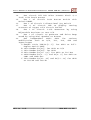
1
User’s Manual of Board Microcontroller “ET-NXP ARM KIT (LPC1768)”
ET-NXP ARM KIT (LPC1768)
ET-NXP ARM KIT (LPC1768) is Board Microcontroller
in the series of ARM Cortex M3 Core that uses 32-Bit
100Pin(LQFP)
Microcontroller
No.LPC1768
from
NXP.
Resources Systems internal LPC1768 are quite perfect
and suitable for learning and testing the operations;
if user learns and understands all resources internal
MCU well, user is able to adapt and apply or develop
many additional applications well. Due to the Hardware
System of LPC1768 includes necessary devices in one MCU
such
ad
USB,
Ethernet,
SD
Card,
ADC,
DAC,
Timer/Counter, PWM, Capture, I2C, SPI, UART, and etc.
That is the reason why ETT studies and researches
on details of LCP1768, we develop and design Board
Microcontroller
version
“ET-NXP
ARM
KIT(LPC1768)”
because we hope that our customers who are interested
in this board will study, test and develop more
applications as preferred under the reasonable price.
Moreover, the main purpose of designing Board ET-NXP
ARM KIT(LPC1768) is to support group of customers who
actually
want
to
study,
test,
adapt
or
apply
application by self. This board’s structure consists of
necessary devices that are suitable for basic test and
study; for example, LED to display Output Logic, Push
Button Switch and Joy Switch to test Logic Input,
ETT Co. Ltd.
1
WWW.ETT.CO.TH
User’s Manual of Board Microcontroller “ET-NXP ARM KIT (LPC1768)”
Volume to adjust voltage for testing A/D, Mini-Speaker
or Buzzer to makes sound or Beep sound. Moreover, it
provides high level devices to support more application
such as USB Device/Host/OTG Port, SD Card, Ethernet LAN
Port, Graphic LCD, RS232, and available free GPIO that
can be designed to use them with other devices as
desired.
Features and Specifications of Board ET-NXP
ARM KIT(LPC1768)
1. Use 32-Bit MCU that is the series of ARM Cortex M3
No.LPC1768 from NXP
2. Has 512KB Flash Memory, 64KB Static RAM internal
MCU
3. Use Crystal 12.00MHz; so, MCU is able to process
data with high speed at 100MHz when using with
Phase-Locked-Loop(PLL) internal MCU itself
4. Has Circuit RTC(Real Time Clock) with XTAL
32.768KHz and Battery Backup
5. Support
In-System
Programming(ISP)
and
InApplication Programming(IAP) through On-Chip BootLoader Software via Port UART0(RS232)
6. Has circuit to connect with the standard 20Pin
JTAG ARM for Real Time Debug
7. Use +5VDC Power Supply from 2 different sources;
from
external
Power
Supply
that
uses
2PIN
Connector and from Connector USB Device with
Circuit Regulate +3V3/3A.
8. Has Circuit USB Device 2.0 Full Speed internally
(USB Function has 32 End Point)
9. Has Circuit USB Host with Circuit Over Current
Protection
10.
Has Circuit USB OTG by using ISP1301 to be
OTG(On-The-Go) Transceiver
11.
Has Circuit Ethernet LAN 10/100MB by using the
standard Connector RJ45 1-Channel
12.
Has Circuit SD Card(Micro-SD) 1-Channel for
SPI Interface
13.
Has Circuit RS232 Communication by using
Connector 4-PIN 2-Channel ETT standard
ETT Co. Ltd.
2
WWW.ETT.CO.TH
User’s Manual of Board Microcontroller “ET-NXP ARM KIT (LPC1768)”
14.
Has circuit TFT LCD Color 320x240 Pixel (3.2
inch) with Touch Screen
15.
Has 1 of Circuit Push Button Switch with
Switch RESET
16.
Has 1 of Circuit 5-directional Joy Switch
17.
Has 8 of Circuit LED to display testing
statuses of Output with Circuit Buffer
18.
Has 1 of Circuit 0-3V3 Generator by using
Adjustable Resistor to test A/D
19.
Has 1 of circuit to generate and drive beep
sound by using Mini Speaker or Buzzer
20.
Has
independent
22Bit
GPIO
for
various
modification such as D/A, I2C, I2S, CAN and
Input/Output
a. Header 10Pin IDE(P2[0..7]) for GPIO or FullDuplex Serial UART
b. 3Pin Header(P0[26]) for GPIO or D/A
c. 3Pin Header(P4[29]) for GPIO
d. 4Pin Header(P0[19..20]) for GPIO or I2C Bus
e. 4PIN Header(P0[0..1]) and P0[4..5] for GPIO or
CAN1 and CAN2 Bus
f. 5Pin Header(P0[23..25] and P2[11..13] for GPIO
or I2S-RX and I2S-TX
ETT Co. Ltd.
3
WWW.ETT.CO.TH
User’s Manual of Board Microcontroller “ET-NXP ARM KIT (LPC1768)”
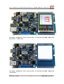
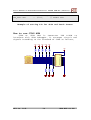
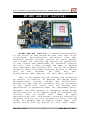
Picture displays the structure of Board ET-NXP ARM KIT
LPC1768 & TFT LCD.
Picture displays the structure of Board ET-NXP ARM KIT
(LPC1768).
ETT Co. Ltd.
4
WWW.ETT.CO.TH
User’s Manual of Board Microcontroller “ET-NXP ARM KIT (LPC1768)”
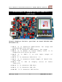
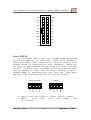
Structure of Board ET-NXP ARM KIT
(LPC1768)
4
6
7
12
9
10
29
28
27
26
23
8
11
5
24
25
13
1
3
2
30
22
17
15
14
16 19
21
18
20
Figure displays device’s position on Board ET-NXP ARM
KIT(LPC1768).
• No.1: It is Connector UART0(RS232) for usage and
Download Hex File into CPU.
• No.2: It is Connector UART2(RS232) for usage.
• No.3: It is Socket to insert memory card, it is
compatible with Micro SD Card.
• No.4: It is LED[0..7] to test Logic Output of
P2[0..7].
• No.5: It is Connector GPIO(P2[0..7]).
• No.6: It is Connector Power Supply of board that
uses +5VDC.
• No.7:
It is
+VDD(+3V3).
LED
to
display
status
of
Power
• No.8: It is connector USB Host.
• No.9: It is Connector USB OTG.
• No.10: It is Connector USB Device.
ETT Co. Ltd.
5
WWW.ETT.CO.TH
User’s Manual of Board Microcontroller “ET-NXP ARM KIT (LPC1768)”
• No.11: It is Jumper(UMODE) to
mode of USB Device connection.
choose
operation
• No.12: It is Jumper(USB) to choose USB Modes
between Device/OTG/Host.
• No.13: Connector Ethernet LAN RJ45.
• No.14: It is Connector JTAG ARM for Real Time
Debug.
• No.15: It is Crystal 32.768KHz to be Time Base for
RTC internal MCU.
• No.16: It is Crystal 12MHz to be Time Base of MCU.
• No.17: It is MCU No.LPC1768 (100Pin LQFP).
• No.18: It is SW RESET.
• No.19: It is SW ISP LOAD or P2.10/EINT0.
• No.20: It is VR to adjust 0-3V3 Voltage to test
A/D(P1[31]/AD0[5]).
• No.21: It is Buzzer to generate sound.
• No.22: It is 5 directional Joy Switch.
• No.23: It is Connector CAN2 or GPIO P0[4..5].
• No.24: It is Connector D/A or GPIO P0.26.
• No.25: It is Connector GPIO P4.29.
• No.26: It is Connector CAN1 or GPIO P0[0..1].
• No.27: It is Connector I2C1-Bus or GPIO
P0[19..20].
• No.28: It is Connector I2STX or GPIO P2[11..13].
• No.29: It is Connector I2SRX or GPIO P0[23..25].
• No.30: It is 320x320 Dot TFT LCD with Touch Screen
Sensor.
ETT Co. Ltd.
6
WWW.ETT.CO.TH
User’s Manual of Board Microcontroller “ET-NXP ARM KIT (LPC1768)”
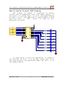
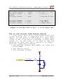
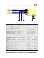
How to drive Circuit LED Display
LED Display of board is connected as Source
Current and is compatible with +3.3V Power Supply; in
this case, it runs by Logic “1”(+3V3) and stops running
by Logic “0”(0V). The operation is controlled by 8 GPIO
that are P2[0..7]. This circuit is used to test
operation of Output.
+VDD
P2.0
P2.1
P2.2
P2.3
P2.4
P2.5
P2.6
P2.7
2
3
4
5
6
7
8
9
19
10
A0
A1
A2
A3
A4
A5
A6
A7
OE
GND
VCC
T/R
B0
B1
B2
B3
B4
B5
B6
B7
74LCX245
20
1
18
17
16
15
14
13
12
11
1K
LED0
1K
LED1
1K
LED2
1K
LED3
1K
LED4
1K
LED5
1K
LED6
1K
LED7
If user wants to use this operation, it needs to
set function of P2[0..7] to be GPIO Output Port first
and then controls the preferred Logic for P2[0..7] as
the example below;
ETT Co. Ltd.
7
WWW.ETT.CO.TH
User’s Manual of Board Microcontroller “ET-NXP ARM KIT (LPC1768)”
// Config Pin GPIO = P2[0..7] Drive LED
LPC_PINCON->PINSEL4 &= ~(0xFFFF); // Reset P2[0..7] = GPIO
LPC_GPIO2->FIODIR
|=
0xFF;
// P2[0..7] =
Outputs
LPC_GPIO2->FIOCLR
=
0xFF;
// Turn-OFF all LED
.
.
LPC_GPIO2->FIOSET
= (1<<0);
// ON LED[0]
LPC_GPIO2->FIOCLR
= (1<<0);
// OFF LED[0]
LPC_GPIO2->FIOPIN
^= (1<<0);
// Toggle LED[0]
Example of setting value of P2[0..7] to be Output LED
How to use Circuit Push Button Switch
This circuit uses Circuit Push Button Switch with
Circuit Pull-Up that is compatible with +3.3V Power
Supply. If this Switch is not pressed, it makes Logic
status “1” but if the Switch is pressed, it makes Logic
status “0”; in this case, it is used to test the
operation of Input Logic and it uses P2.10 to connect.
There are 3 functions as follows;
• ISP Download through RS232(UART0) by using with
Switch RESET
• Test Input of P2[10]
• Test Interrupt of EINT0
+VDD
10K
ISP-BOOT
P2.10(EINT0)
470
8
ISP LOAD
0.1uF
ETT Co. Ltd.
WWW.ETT.CO.TH
User’s Manual of Board Microcontroller “ET-NXP ARM KIT (LPC1768)”
LPC_PINCON->PINSEL4 &= ~(0x03<<20);
GPIO
LPC_GPIO2->FIODIR
&= ~(1UL<<10);
.
.
if ((LPC_GPIO2->FIOPIN >> 10) & 0x01)
{
...
}
else
{
...
}
// Reset P2.10 =
// P2.10 = Input
//SW = Release
// SW = Press
Example of setting values of P2.10 to be Input Switch
How to use Circuit Joy Switch
This circuit uses 5 directional Joy Switch and its
structure is Push Button with Circuit Pull-Up that is
compatible with +3.3V Power Supply. If this Switch is
not pressed, it makes Logic status “1” but if the
Switch is pressed, it makes Logic status “0”; in this
case, it is used to test the operation of Input Logic.
Moreover, it can be modified for other application by
connecting signal through GPIO Input as follows;
• Up Position uses P1.25 to be GPIO Input.
• Down Position uses P1.26 to be GPIO Input.
• Right Position uses P1.28 to be GPIO Input.
• Left Position uses P1.29 to be GPIO Input.
• Center Position uses P3.25 to be GPIO Input.
ETT Co. Ltd.
9
WWW.ETT.CO.TH
User’s Manual of Board Microcontroller “ET-NXP ARM KIT (LPC1768)”
+VDD
+VDD
+VDD
10K
10K
10K
10K
P1.25(GPIO:IN)
P1.28(GPIO:IN)
P3.25(GPIO:IN)
P1.29(GPIO:IN)
P1.26(GPIO:IN)
+VDD
10K
JOY-UP
JOY-RGT
JOY-ENT
JOY-LFT
JOY-DN
+VDD
470R x 5
LPC_PINCON->PINSEL7 &= ~(0x03<<18);
LPC_GPIO3->FIODIR
&= ~(1UL<<25);
.
.
//Joy Up = P1.25
if ((LPC_GPIO1->FIOPIN >> 25) & 0x01)
0.1uF
0.1uF
0.1uF
0.1Uf
01.uF
//Joy Switch
//P1.25,P1.26,P1.28,P1.29,P3.25 = Joy Switch
LPC_PINCON->PINSEL3 &= ~(0x03<<18);
LPC_PINCON->PINSEL3 &= ~(0x03<<20);
LPC_PINCON->PINSEL3 &= ~(0x03<<24);
LPC_PINCON->PINSEL3 &= ~(0x03<<26);
LPC_GPIO1->FIODIR
&= ~((1UL<<25)|(1UL<<26)|
(1UL<<28)|(1UL<<29));
//P1.25,26,28,29=In
//P1.25
//P1.26
//P1.28
//P1.29
=
=
=
=
GPIO
GPIO
GPIO
GPIO
//P3.25 = GPIO
//P3[25]= Input
// SW = Release
{
...
}
else
{
...
}
// SW = Press
//Joy Down = P1.26
if ((LPC_GPIO1->FIOPIN >> 26) & 0x01)
// SW = Release
{
...
}
else
{
...
}
ETT Co. Ltd.
// SW = Press
10
WWW.ETT.CO.TH
User’s Manual of Board Microcontroller “ET-NXP ARM KIT (LPC1768)”
//Joy Right = P1.28
if ((LPC_GPIO1->FIOPIN >> 28) & 0x01)
.
.
.
.
.
//Joy Center = P3.25
if ((LPC_GPIO3->FIOPIN >> 25) & 0x01)
// SW = Release
// SW = Release
{
...
}
else
{
...
}
// SW = Press
Example of setting values for Input Joy Switch
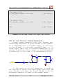
How to use Circuit Sound Generator
Circuit Sound Generator uses Mini Speaker with
Circuit NPN Transistor to drive current to the speaker.
It is compatible with +3.3V Power Supply; in this case,
it runs by Logic “1” and stops running by Logic “0”. It
sends Signal Logic that is various frequencies to the
speaker to generate various ranges of sound frequencies
as preferred; in this case, it is controlled by P3[26].
+VDD
BUZZER
10R
4148
10K
4148
P3.26(GPIO:OUT)
BC807
2K2
If user wants to use this operation, it needs to
set function of P3[28] to be GPIO Output Port first and
then controls the Logic for P3[28] ON/OFF to be the
preferred frequency as shown in the example below.
ETT Co. Ltd.
11
WWW.ETT.CO.TH
User’s Manual of Board Microcontroller “ET-NXP ARM KIT (LPC1768)”
//Config Pin GPIO = P3[26] Drive Mini Speaker Generate Beep
LPC_PINCON->PINSEL7 &= ~(3 << 20);
// Reset P3.26 = GPIO
LPC_GPIO3->FIODIR
|= (1UL<<26);
// P3[26] = Output
// Loop Generate Beep on Speaker(P3.26)
while(1)
{
for (i = 0; i < 500; i++)
{
LPC_GPIO3->FIOPIN ^= (1 << 26);
delay(5000);
}
// Loop Continue
// Start Beep Pulse
// Toggle P3[26]
delay(10000000);
// Stop Beep Pulse
}
Example of setting values of P3.26 to be Output to
drive the Buzzer
How to use
3V3)
Circuit
Adjustable
Voltage (0-
Circuit Adjustable Voltage uses VR that is
compatible with +3.3V Power Supply. It uses Output
Voltage in the range of 0V to +3.3V according to the
adjustment of Resistor. This Output value will be
inputted to Pin P1[31] to generate Input Voltage for
testing the operation of Circuit A/D(P1[31]).
+VDD
P1.31(AD0.5)
470
10K
ADC
0.1Uf
ETT Co. Ltd.
12
WWW.ETT.CO.TH
User’s Manual of Board Microcontroller “ET-NXP ARM KIT (LPC1768)”
LPC_PINCON->PINSEL3
LPC_PINCON->PINSEL3
AD0.5
LPC_SC->PCONP
ADC
LPC_ADC->ADCR
18MHz/2
&= ~(3UL<<30);
|= (3UL<<30);
// Reset P1.31 = GPIO
// Config P1.31 =
|=
(1UL<<12);
// Enable power to
=
(1UL<< 5) |
(1UL<< 8) |
// select AD0.5 pin
// ADC clock is
(1UL<<21);
// enable ADC
unsigned int val;
.
.
while(1)
{
LPC_ADC->ADCR |= (1<<24);
while (!(LPC_ADC->ADGDR & (1UL<<31)));
end
val = ((LPC_ADC->ADGDR >> 4) & 0xFFF);
value
LPC_ADC->ADCR &= ~(7<<24);
.
.
.
}
// start conversion
// Wait Conversion
// read converted
// stop conversion
Example of setting values for P1.31 to be Analog Input
AD0.5
How to use Graphic TFT LCD
There are 2 types to connect circuit of Board ETNXP ARM KIT(LPC1768) with 3.2” Graphic TFT LCD as
described below;
• It permanently installs Module LCD on Board by
using TFT LCD “KWH032GM02-F05” and it connects
signal with TFT LCD in SPI mode; moreover, this
TFT LCD version has included Sensor of Touch
Screen completely. The device of Board ET-NXP ARM
KIT(LPC1768) that is used to read Sensor of Touch
Screen is designed to choose Chip numbers as
preferred; in this case, it uses Chip No.STMPE811
ETT Co. Ltd.
13
WWW.ETT.CO.TH
User’s Manual of Board Microcontroller “ET-NXP ARM KIT (LPC1768)”
for I2C Interface or it uses Chip ADS7846 for SPI
Interface (it depends on chip type that is
installed in board in the process of making
board).
• It installs Board Display “ET-TFT240320TP-3.2
REV.B” from ETT that has already been installed
TFT LCD “KWH032GM02-F05” with Chip ADS7846 to read
Touch Sensor internal board completely. It is
installed through Connector; moreover, it is able
to add or remove the device from board easily. In
this case, it needs to set the format of Interface
with board to be SPI.
ETT Co. Ltd.
14
WWW.ETT.CO.TH
User’s Manual of Board Microcontroller “ET-NXP ARM KIT (LPC1768)”
↓
ETT Co. Ltd.
15
WWW.ETT.CO.TH
User’s Manual of Board Microcontroller “ET-NXP ARM KIT (LPC1768)”
How to connect TFT LCD “KWH032GM02-F05”
TFT LCD “KWH032GM02-F05” is interfaced as SPI Mode
by using SSP1 of MCU to communicate; in this case, it
connects signals as follows;
• CS GLCD uses P0.6 to be GPIO Output.
• SCL GLCD uses P0.7 to be SCK1 of SSP1.
• SDO GLCD uses P0.8 to be MISO1 of SSP1.
• SDI GLCD uses P0.9 to be MOSI1 of SSP1.
• BL GLCD uses P4.28 to be GPIO Output.
How to
ADS7846
connect
Touch
Screen
Sensor
by
If Touch Screen uses Chip ADS7846, it is SPI
Interface and it uses SSP0 of MCU to communicate. It
connects signals as follows;
• DCLK ADS7846 uses P1.20 to be SCK0 of SSP0.
• CS ADS7846 uses P1.21 to be GPIO Output.
• DOUT ADS7846 uses P1.23 to be MISO0 of SSP0.
• DIN ADS7846 uses P1.24 to be MOSI0 of SSP0.
• PENIRQ ADS7846 uses P0.21 to be GPIO Input.
How to
STMPE811
connect
Touch
Screen
Sensor
by
If Touch Screen uses Chip STMPE811, it is I2C
Interface that has Address position of Device for I2C
Interface as 0x82. It uses I2C1 of MCU to communicate
and it connects signals as follows;
• SDAT STMPE811 uses P0.19 to be SDA1 of I2C1.
• SCLK STMPE811 uses P0.20 to be SCL1 of I2C1.
• INT STMPE811 uses P2.8 to be GPIO Input.
/* Config P1[20..24] to SSP0 For Read
LPC_PINCON->PINSEL3 &= ~(3UL<<10);
LPC_GPIO1->FIODIR
|= (1UL<<21);
CS(Output)
LPC_GPIO1->FIOPIN
|= (1UL<<21);
Touch LCD(ADS7846) */
// Reset P1.21 Mode = GPIO
// P1.21 = ADS7846
LPC_PINCON->PINSEL1 &= ~(3UL<<10);
// Reset P0.21 Mode = GPIO
ETT Co. Ltd.
16
// P1.21 = High
WWW.ETT.CO.TH
User’s Manual of Board Microcontroller “ET-NXP ARM KIT (LPC1768)”
LPC_GPIO0->FIODIR
&= ~(1UL<<21);
//Config SSP0 Pin Connect
LPC_PINCON->PINSEL3 |= (3UL<<8);
SCK0(SSP0)
LPC_PINCON->PINSEL3 |= (3UL<<14);
MISO0(SSP0)
LPC_PINCON->PINSEL3 |= (3UL<<16);
MOSI0(SSP0)
LPC_SC->PCONP
block
LPC_SC->PCLKSEL1
LPC_SC->PCLKSEL1
LPC_SSP0->CPSR
2MHz)
|=
(1<<21);
=
LPC_SSP0->CR1
=
(
0 <<
(
0 <<
(
0 <<
((8-1)<<
(
1 <<
// Select P1.20 =
// Select P1.23 =
// Select P1.24 =
// Enable power to SSPI0
&= ~(3<<10);
|= (1<<10);
=
72;
LPC_SSP0->CR0
// P0.21 = PENIRQ(Input)
// PCLKSP0 = CCLK/4 (18MHz)
// PCLKSP0 = CCLK
(72MHz)
// 72MHz / 72 = 1MHz(max
7) |
6) |
4) |
0);
1);
//
//
//
//
//
CPHA = 0
CPOL = 0
Frame format = SPI
Data size = 8 bits
Enable SSP0
/* Config P0.6,P0.7,P0.8,P0.9 to SSP1
LPC_PINCON->PINSEL9 &= ~(3 << 24);
LPC_GPIO4->FIODIR
|= (1UL<<28);
LPC_GPIO4->FIOPIN
&= ~(1UL<<28);
For Control GLCD */
// Reset P4.28 Mode = GPIO
// Pin P4.28 = Output(BL)
// Turn-OFF GLCD Backlight
LPC_PINCON->PINSEL0 &= ~(3UL<<12);
LPC_GPIO0->FIODIR
|= (1 << 6);
GLCD)
LPC_GPIO0->FIOSET
= (1 << 6);
// Reset P0.6 Mode = GPIO
// P0.6 = GPIO output(CS
LPC_PINCON->PINSEL0
LPC_PINCON->PINSEL0
LPC_PINCON->PINSEL0
LPC_PINCON->PINSEL0
MISO1(SSP1)
LPC_PINCON->PINSEL0
LPC_PINCON->PINSEL0
MOSI1(SSP1)
&= ~(3UL<<14);
|= (2UL<<14);
&= ~(3UL<<16);
|= (2UL<<16);
//
//
//
//
&= ~(3UL<<18);
|= (2UL<<18);
// Reset P0.9 Mode = GPIO
// Select P0.9 =
LPC_SC->PCONP
block
LPC_SC->PCLKSEL0
(36MHz)
LPC_SSP1->CPSR
|=
(1 << 10);
// Enable power to SSP1
|=
(2 << 20);
// SSP1 clock = CCLK/2
=
2;
// Clock Rate = 18MHz
=
(1<<7) |
(1<<6) |
(0<<4) |
// CPHA = 1
// CPOL = 1
// Frame format = SPI
LPC_SSP1->CR0
ETT Co. Ltd.
17
// Set P0.6 = High
Reset P0.7 Mode = GPIO
Select P0.7 = SCK1(SSP1)
Reset P0.8 Mode = GPIO
Select P0.8 =
WWW.ETT.CO.TH
User’s Manual of Board Microcontroller “ET-NXP ARM KIT (LPC1768)”
LPC_SSP1->CR1
=
((8-1)<< 0);
(1<<1);
// Data size = 8 bits
// Enable SSP1
Example of setting Pin for GLCD and Touch Screen
How to use JTAG ARM
JTAG or JTAG ARM is Connector IDE 20PIN to
interface with JTAG Debugger. It arranges circuit and
signals according to the standard of JTAG as follows;
+VDD +VDD +VDD +VDD +VDD
10K
10K
10K
10K
10K
+VDD
1
3
5
7
9
11
13
15
17
19
JTAG-TRST#
JTAG-TDI
JTAG-TMS
JTAG/TCK
JTAG-RTCK
JTAG-TDO
RESET#
2
4
6
8
10
12
14
16
18
20
JTAG ARM
10K
18
10K
10K
ETT Co. Ltd.
WWW.ETT.CO.TH
User’s Manual of Board Microcontroller “ET-NXP ARM KIT (LPC1768)”
VTref
TRST
TDI
VTarget
GND
GND
TMS
TCK
RTCK
GND
GND
GND
TDO
RES#
NC
GND
GND
GND
NC
GND
ARM JTAG Pin Connector
Port RS232
It is Signal RS232 that has already been converted
by Circuit MAX3232; in this case, there are 2 channels;
UART0 and UART2. Both channels are able to connect with
Signal RS232 to send/receive data. Moreover, UART0 can
be used as ISP Download to download Hex File into MCU
as well; in this case, it needs to use with SW ISP LOAD
and SW RESET to reset CPU to start running in BootLoader Mode to download Hex File into CPU (read more
details from “Download Hex File to MCU of Board”)
4
RXD0
TXD0
GND
1
2
3
4
GND
3
TXD2
2
UART2
+3V3
RXD2
1
+3V3
UART0(Download)
• UART-0 uses Pin from P0.2(TXD0) and P0.3(RXD0).
• UART-2
uses
Pin
from
P0.10(TXD2)
and
P0.11(RXD2).
ETT Co. Ltd.
19
WWW.ETT.CO.TH
User’s Manual of Board Microcontroller “ET-NXP ARM KIT (LPC1768)”
Due to the Hardware UART System of LPC1768/LPC2387
can set many connecting points of pin to connect; for
example, UART2 can choose either Pin P0[10] and P0[11]
or P2[8] and P2[9] as required. Board ET-NXP ARM KIT
chooses Pin P0[10] and P0[11] to be the connecting
point with UART2; so, user needs to set the command to
choose pin correctly. Be careful about using UART, the
Default value of UART2 is disabled; so, user needs to
enable the operation of Circuit UART2 before using the
command Initial for UART. Otherwise, user is unable to
command any UART. The example Code of setting the UART
value in the initial part is shown below;
// Config UART0 Connect to P0[2]:P0[3]
LPC_PINCON->PINSEL0 &= ~(0x03<<4);
LPC_PINCON->PINSEL0 |= (0x01<<4);
LPC_PINCON->PINSEL0 &= ~(0x03<<6);
LPC_PINCON->PINSEL0 |= (0x01<<6);
//
//
//
//
Reset P0.2 = GPIO
Config P0.2 = TxD0
Reset P0.3 = GPIO
Config P0.3 = RxD0
// Config UART2 Connect to P0[10]:P0[11]
LPC_PINCON->PINSEL0 &= ~(0x03<<20);
LPC_PINCON->PINSEL0 |= (0x01<<20);
LPC_PINCON->PINSEL0 &= ~(0x03<<22);
LPC_PINCON->PINSEL0 |= (0x01<<22);
PCONP
|= 0x01000000;
//
//
//
//
//
Reset P0.10 = GPIO
Config P0.10 = TxD2
Reset P0.11 = GPIO
Config P0.11 = RxD2
UART2 Power-ON
Example of setting Pin for UART0 and UART1
Figure below displays the Cable that is connected
RS232 between Com Port of computer PC and Connector
UART0 and UART2 of Board ET-NXP ARM KIT.
ETT Co. Ltd.
20
WWW.ETT.CO.TH
User’s Manual of Board Microcontroller “ET-NXP ARM KIT (LPC1768)”
1
6
2
7
3
8
4
9
5
CD
DSR
RXD
RTS
TXD
CTS
DTR
RI
GND
1
2
3
4
RXD
TXD
GND
ET-RS232
DB9(FEMALE)
RS232-PC
1
14
2
15
3
16
4
17
5
18
6
19
7
20
8
21
9
22
10
23
11
24
12
25
13
TXD
RXD
RTS
CTS
DSR
1
2
3
4
RXD
TXD
GND
GND
DTR
ET-RS232
DB25(FEMALE)
RS232-PC
Figure displays Circuit of cable for RS232.
ETT Co. Ltd.
21
WWW.ETT.CO.TH
User’s Manual of Board Microcontroller “ET-NXP ARM KIT (LPC1768)”
Ethernet LAN
It uses the standard Connector Ethernet RJ45 to
connect the Network System and Board ET-NXP ARM
KIT(LPC1768).
This
circuit
uses
Pin
P1[0,1,4,8,9,10,14..17] and Chips Physical Ethernet
No.DP83848 to be Driver for connection.
There are 2 methods to connect Cable Ethernet LAN
of Board with the Network System; Direct Line Interface
and HUB Interface.
• Case 1: It directly connects to computer and Cable
LAN is connected as Cross type.
• Case 2: It is connected through HUB of computer
Server and it is connected as Direct type.
ETT Co. Ltd.
22
WWW.ETT.CO.TH
User’s Manual of Board Microcontroller “ET-NXP ARM KIT (LPC1768)”
How to use USB
Board ET-NXP ARM KIT(LPC1768) has Port that can be
connected with USB Device either USB Host or USB
OTG(On-The-Go), depends on writing program to set
function of USB internal MCU of LPC1768. In the part of
Hardware, user needs to set Jumper to choose the
connection between Signal USB of MCU LPC1768 and
Circuit of USB Port; in this case, it needs to set the
values according to the real usage. There are 3 types
of USB Connection as follows;
HOST
OTG
DEVICE
It chooses USB Mode to be USB DEVICE.
HOST
OTG
DEVICE
It chooses USB Mode to be USB OTG.
HOST
OTG
DEVICE
It chooses USB Mode to be USB HOST.
ETT Co. Ltd.
23
WWW.ETT.CO.TH
User’s Manual of Board Microcontroller “ET-NXP ARM KIT (LPC1768)”
USB Device Mode
This operation mode uses
it needs to program function
with USB Bus as follows;
• USB D(+) uses P0.29 for
Device Mode.
• USB D(-) uses P0.30 for
Device Mode.
• USB CONNECT uses P2.9 for
LED) of USB Device Mode.
5 Cables to connect and
of each pin to connect
Function USB_D+ of USB
Function USB_D- of USB
Function USB_CONNECT(USC
• USB UP LED P1.18 ในหนาที่ USB_UP_LED(UGL LED) ของ USB Device Mode
• USB UP LED uses P1.18 for Function USB_UP_LED(UGL
LED) of USB Device Mode.
• USB VBUS จะใช P1.30 ในหนาที่ USB VBUS ของ USB Device Mode
• USB VBUS uses P1.30 for Function USB VBUS of USB
Device Mode.
If it is USB Device, there is Jumper UMODE to
choose the connection with USB Host either Direct
Connect or Soft Connect by using P2.9(USB_CONNECT) to
be Pin Control of the connection. If it chooses Soft
Connect, it needs to set Jumper UMODE to the side of
P2.9 and then write program to set function of P2.9 to
control the connection between USB Device and Bus.
However, if user does not choose Soft Connect, it needs
to set Jumper UMODE to the side of GND to enable the
connection between USB Device and Bus all the time. In
this case, there is LED USC to display status of
signal; this LED USC is ON when the signal that
controls the connection of USB Device is in the status
of Active.
This USB Device Mode has 2 LED to display
operating status of USB as follows;
• USC: It displays operating status of signal that
controls Connect Bus and it will be ON when the
Connect Bus is enabled.
• UGL: It displays operating status when the
connection between USB Device and Host Bus is
successful.
ETT Co. Ltd.
24
WWW.ETT.CO.TH
User’s Manual of Board Microcontroller “ET-NXP ARM KIT (LPC1768)”
USB OTG Mode (USB On-The-Go)
This operation mode uses 5 Cables to connect and
it uses Chip ISP1301 to be USB OTG Transceiver. It
needs to program function of each pin to connect with
USB Bus as follows;
• USB D(+) uses P0.29 for Function USB_D+ of USB OTG
Mode.
• USB D(-) uses P0.30 for Function USB_D- of USB OTG
Mode.
• USB SDA uses P0.27 for Function USB_SDA of USB OTG
Mode.
• USB SCL uses P0.28 for Function USB_SCL of USB OTG
Mode.
• USB INT uses P0.22 for Function GPIO Input.
This USB OTG Mode has 2 LED to display operating
status of USB as follows;
• VOTG: It displays operating status of VBUS of USB
Vbus.
• UGL: It displays operating status when USB Bus and
external device are connected successfully.
USB Host Mode
This operation mode uses 5 Cables to connect and
it uses Chip TPS2055 or TPS2031 to controls VBUS of
Host;
moreover,
it
also
is
Host
Over
Current
Protection. It needs to program function of each pin to
connect with USB Bus as follows;
• USB D(+) uses P0.29 for Function USB_D+ of USB
Host Mode.
• USB D9(-) uses P0.30 for Function USB_D- of USB
Host Mode.
• USB OVRCR uses P1.27 for Function USB_OVRCR of USB
Host Mode.
• USB PPWR uses P1.19 for Function USB_PPWR of USB
Host Mode.
• USB UP LED uses P1.18 for Function USB_UP_LED(UGL
LED) of USB Host Mode.
ETT Co. Ltd.
25
WWW.ETT.CO.TH
User’s Manual of Board Microcontroller “ET-NXP ARM KIT (LPC1768)”
This USB Host Mode has 3 LED to display operating
result of USB as follows;
• VHOST: It displays VBUS status of USB Host Bus and
it will be ON when the circuit supplies VBUS to
Host Port.
• OVC: It displays operating status when it pulls
current from USB Host Port higher than the
specified value. When this LED is ON, Output Logic
“0” is sent to OVRCE(P1.27) of MCU to notify MCU
to know.
• UGL: It displays operating status when USB Host
Bus
and
external
device
are
connected
successfully.
Micro-SD Card
Board
ET-NXP
ARM
KIT(LPC1768)
supports
the
connection with Micro-SD Card in the format of SPI
Interface and it uses Pin P0[15..18] to connect with
card. When user wants to command the card, it is able
to program Pin I/O of P0[15..18] to operate in SPI Mode
and it needs to set the function of Pin P0[15..18] of
MCU as follows;
• CLK uses P0.15 for Function SCK of SPI.
• CD/DAT3 uses P0.16 for Function GPIO Output.
• DAT0 uses P0.17 for Function MISO of SPI.
• CMD uses P0.18 for Function MOSI of SPI.
ETT Co. Ltd.
26
WWW.ETT.CO.TH
User’s Manual of Board Microcontroller “ET-NXP ARM KIT (LPC1768)”
+VDD
MICRO SD-3M
SD-MISO
P0.15(SPI:SCK)
P0.17(SPI:MISO)
DAT2
CD/DAT3
CMD
VDD
CLK
VSS
DAT0
DAT1
GND
GND
GND
GND
SD-SCK
P0.16(GPIO:OUT)
P0.18(SPI:MOSI)
0.1uF
10uF
G1
G2
G3
G4
SD-CS
SD-MOSI
1
2
3
4
5
6
7
8
//Config P0.15,P0.16,P0.17,P0.18 = SPI Interface
LPC_SC->PCONP
|= (1 << 8);
//Enable power to SPI
LPC_SC->PCLKSEL0
&=
~(3<<16);
//PCLK_SPI=CCLK/4(18MHz)
LPC_SC->PCLKSEL0
|=
(1<<16);
//PCLK_SPI=CCLK(72MHz)
LPC_SPI->SPCCR = 180;
//72MHz/180=400kBit
// SSEL is GPIO, output set to high.
LPC_GPIO0->FIODIR |= (1<<16);
LPC_GPIO0->FIOPIN |= (1<<16);
LPC_PINCON->PINSEL1 &= ~(3<<0);
// SCK, MISO, MOSI are SSP pins.
LPC_PINCON->PINSEL0 &= ~(3UL<<30);
LPC_PINCON->PINSEL0 |= (3UL<<30);
LPC_PINCON->PINSEL1 &= ~((3<<2)|(3<<4));
cleared
LPC_PINCON->PINSEL1 |= ((3<<2)|(3<<4));
MOSI
//Config SPI = Master,8Bit,CPOL=0,CPHA=0
LPC_SPI->SPCR &= ~(1<<3);
Clock
LPC_SPI->SPCR &= ~(1<<4);
LPC_SPI->SPCR |= (1<<5);
SPI
LPC_SPI->SPCR &= ~(1<<6);
First
LPC_SPI->SPCR &= ~(1<<7);
INT
ETT Co. Ltd.
27
//P0.16 is output
//set P0.16 = high
//P0.16 = GPIO
//P0.15 cleared
//P0.15 SCK
//P0.17,
//P0.17
//CPHA
MISO,P0.18
=
0
//CPOL = 0
//MSTR = 1
//LSBF
P0.18
=
=
0
Rising
Master
=
MSB
//SPIE = 0 = Disable
WWW.ETT.CO.TH
User’s Manual of Board Microcontroller “ET-NXP ARM KIT (LPC1768)”
LPC_SPI->SPCR &= ~(15<<8);
Format)
LPC_SPI->SPCR |= (1<<11);
Data)
LPC_SPI->SPCR |= (1<<2);
//BIT
//BIT
=
=
0000(Bits
1000(8
Bit
//Enable SPI
Example of setting Pin for SD Card
Connector Port I/O of Board
Port I/O of CPU is arranged at connectors, so user
can choose them as preferred; in this case, there are 8
sets as shown below;
• Has 2 sets of Connector IDE 10Pin; in this case,
there are 8Bit per each set; P2[0..7]. Signal are
arranged as below;
P2.0
P2.2
P2.4
P2.6
+3V3
P2.1
P2.3
P2.5
P2.7
GND
P2[0..7]
• Connector DAC is Header 1x3 that is used to be the
connecting point P0[26]; in this case, it can be
used either general GPIO or D/A(Aout) as required.
o P0.26 = AOUT or D/A
ETT Co. Ltd.
2
3
GND
+3V3
1
P0.26
DAC
28
WWW.ETT.CO.TH
User’s Manual of Board Microcontroller “ET-NXP ARM KIT (LPC1768)”
• Connector GPIO is Header 1x3 that is used to be
the connecting point P4[29]; in this case, it can
be used either general GPIO or other functions
according to the Config value of P4[29] as
required.
o P4.29 = GPIO
1
2
3
+3V3
P4.29
GND
GPIO
• Connector I2C-1 is Header 1x4 that is used to be
the connecting point P0[19..20]; in this case, it
can be used either general GPIO or I2C Bus as
required.
o P0.19 = SDA1
o P0.20 = SCL1
1
2
3
4
+3V3
P0.19
P0.20
GND
I2C1
• Connector CAN-1 is Header 1x4 that is used to be
the connecting point P0[0..1]; in this case, it
can be used either general GPIO or Can Bus(CAN-1)
as required.
o P0.0 = RD1
o P0.1 = TD1
1
2
3
4
+3V3
P0.0
P0.1
GND
CAN1
• Connector CAN-2 is Header 1x4 that is used to be
the connecting point P0[4..5]; in this case, it
ETT Co. Ltd.
29
WWW.ETT.CO.TH
User’s Manual of Board Microcontroller “ET-NXP ARM KIT (LPC1768)”
can be used either general GPIO or Can Bus(CAN-2)
as required.
o P0.4 = RD2
o P0.5 = TD2
P0.4
3
4
GND
2
P0.5
1
+3V3
CAN2
• Connector I2SRX is Header 1x5 that is used to be
the connecting point P0[23..25]; in this case, it
can be used either general GPIO or I2SRX as
required.
o P0.23 = RXCLK
o P0.24 = RXWS
o P0.25 = RXSDA
I2SRX
4
5
GND
3
P0.24
P0.23
2
+3V3
P0.25
1
• Connector I2STX is Header 1x5 that is used to be
the connecting point P2[11..13]; in this case, it
can be used either general GPIO or I2STX as
required.
o P2.11 = TXCLK
o P2.12 = TXWS
o P2.13 = TXSDA
I2STX
ETT Co. Ltd.
4
30
5
GND
3
P0.12
P0.11
2
+3V3
P0.13
1
WWW.ETT.CO.TH
User’s Manual of Board Microcontroller “ET-NXP ARM KIT (LPC1768)”
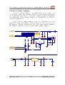
Circuit Power Supply
Circuit Power Supply is compatible with +5VDC; in
this case, user can choose source either from Connector
or from USB Device to interface Power Supply to board
as required. This Power Supply is connected to Circuit
+3V3/3A Regulate.
The Circuit Power Supply that is the part of 3.3V
Regulate supplies power to CPU and all of Circuit I/O
of board, except Backlight of LCD and Buzzer/Speaker
because it directly uses +5VDC from Power Supply.
4K7
P1.30(VBUS)
DEVICE
VBUS
DD+
GND
33R
+VDD
+VDD
33R
1K5
1K
1M
P1.18(USB_UP_LED)
10K
P2.9(USB_CONNECT)
2K2
UMODE
+5V
+VDD
VIN
+5V
3
IN
1
+3V3
31
1K
2
0.1uF
10uF
10uF
ETT Co. Ltd.
OUT
1000uF
SS14
GND
LD1085-3V3
1
2
4n7
BC807
USC
USB-CONNECT
18pF
18pF
1K
UGL
USB-UPLED
+VDD
USB-DEVICE
1
2
3
4
WWW.ETT.CO.TH
5
P0.29:USB_D+
P0.30:USB_D-
0.1uF
OTG
USB-DP
USB-DM
SS14
DH+
DHDO+
DO-
220K
DH+
DHDO+
DODP+
DM-
HOST
500mA
6
USB-VBUS
User’s Manual of Board Microcontroller “ET-NXP ARM KIT (LPC1768)”
How to download Hex File to MCU on Board
The method to download HEX File into Flash Memory
of MCU on board is to use Program Flash Magic of
“Embedded System Academy,Inc” and it is connected with
MCU through Serial Port of computer PC. This program
can be downloaded free from website: www.esacademy.com.
Procedures of downloading HEX File to MCU
1. Connect Cable RS232 between RS232 Serial Port
Communication of PC and Board UART0.
2. Supply power into board; user can see status of
LED PWR to be ON.
3. Run Program Flash Magic; if it is Version
5.39.1797, it will display operating results as
below;
ETT Co. Ltd.
32
WWW.ETT.CO.TH
User’s Manual of Board Microcontroller “ET-NXP ARM KIT (LPC1768)”
4. Start setting initial values into program as
required; if using with LPC1768 of Board ET-NXP
ARM KIT(LPC1768) from ETT, it chooses and sets
values into program as follows;
• Choose COM Port according to the real COM Port
number that is actually is connected on board
(this example is COM4)
• Should set Baud Rate in the range of 2400115200; if it sets Baud Rate too high, it
maybe error. So, it is better to reduce Baud
Rate lower, this example is 115200.
• Set Device as LPC1768.
• Set Interface as None ISP.
• Set Crystal Oscillator according to the real
value that is actually is used on board with
the unit of MHz; in this case, it uses
12.000MHZ, so it is set as 12.
• Press Switch ISP LOAD and Switch RESET on
Board “ET-NXP ARM KIT” to reset MCU to run in
Boot Loader as described below
Press and hold Switch ISP LOAD for a
while.
Press Switch RESET and Switch ISP LOAD
is still pressed.
Release Switch RESET but Switch ISP LOAD
is still pressed.
Finally, release Switch ISP LOAD.
5. Choose the format of erasing data as “Erase all
Flash + Code Rd Prot”.
6. Choose Option as “Verify after programming”.
7. Click “Browse” to choose the preferred HEX File
for downloading.
8. Click “Start”, it makes Program Flash Magic start
downloading data into MCU instantly and user can
see the operating results through Status Bar. In
this case, user needs to wait until all operation
of program is complete.
ETT Co. Ltd.
33
WWW.ETT.CO.TH
User’s Manual of Board Microcontroller “ET-NXP ARM KIT (LPC1768)”
9. When the program run successfully, press Switch
RESET on board and it makes MCU start operating
according to the downloaded program instantly.
ETT Co. Ltd.
34
WWW.ETT.CO.TH