1
University of Waterloo
Electrical and Computer Engineering
Department
Digital Computers
ECE-222 Lab manual
Version 1.70
Released on November 20, 2012
Developed by: Rasoul Keshavarzi, Hiren D. Patel
Assisted by: Roger Sanderson, Eric Praetzel, Gordon B. Agnew
This manual is for the exclusive use of students registered in the course.
Reproduction or use for any other purpose is prohibited.
1
2
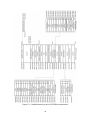
Contents
General Information .......................................................................................................................................... 3
Lab schedule .................................................................................................................................................. 3
Lab groups ..................................................................................................................................................... 4
Lab marking ................................................................................................................................................... 4
Due dates and on-time delivery .................................................................................................................... 4
Lab-0: Introduction to the ARM platforms in the lab........................................................................................ 5
Lab-1: Flashing LED .......................................................................................................................................... 13
Lab-2: Subroutines and parameter passing..................................................................................................... 17
Lab-3: Input/Output interfacing ...................................................................................................................... 23
Lab-4: Interrupt handling ................................................................................................................................ 27
Appendix A: The LPC1768 microprocessor ..................................................................................................... 30
Appendix B: Instruction set summary ............................................................................................................. 33
Appendix C: Memory map............................................................................................................................... 40
Appendix D: Input / Output ports ................................................................................................................... 42
Appendix E: Exception and Interrupts ............................................................................................................. 48
Appendix F: Schematic diagram [4] ................................................................................................................. 50
References: ...................................................................................................................................................... 56
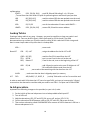
General Information
All lab content and resources are posted on Waterloo LEARN. It is here: learn.uwaterloo.ca
For the Fall 2012 term we are shifted from the ColdFire® to ARM® boards for the ECE-222 lab. You
may come across some typos or errors in this manual. Please report such cases to the Lab
Instructor. We appreciate your feedback and cooperation.
Lab schedule
The exact dates for labs can be found here:
http://www.adm.uwaterloo.ca/infocour/CIR/SA/under.html
3
Lab groups
All labs are to be done in groups of two students. Groups of more students are prohibited.
It is expected that both members will put equal effort into the lab. Unequal participation or other
conflicts in a group should be brought to the lab instructor’s attention at the earliest possible time.
Lab marking
There are three marked components related to each lab session. The lab manual for each
experiment will tell you what you will need to submit for that component.
-
Prelab. It is designed to get you started with the task. Once completed, you will be ready to
start coding in assembly language.
Lab session/Demo. You will present your work to a lab staff to be marked for that section.
Lab report. You will submit a report containing your assembly language code, to be marked
by a TA.
Different labs carry different marks allocated to them.
Warning: Failure to attend and complete ALL labs may result in an ‘Incomplete’ mark.
Due dates and on-time delivery
Lab reports and lab demonstration sessions will have marks associated with them. If you miss a lab
session, please inform the lab instructor to avoid being recorded as ‘Absent’. They will try to assign
you to another session for that particular lab.
Electronic lab report submission is done through ECE CourseBook
(https://ecewo32.uwaterloo.ca/cgi-bin/WebObjects/CourseBook) or possibly UW Learn
(learn.uwaterloo.ca). Lab reports are due 48 hours after your scheduled lab session. A penalty,
per day, will be applied to late reports.
4
Lab-0: Introduction to the ARM platforms in the lab
Objective
We will familiarize ourselves with the basics of the ARM boards used in the ECE-222 lab. Here is a
short list of what we will do in this session:
-
Introduction to ARM board
Introduction to µVision4 software
o How to create or open a project
o How to build, or assemble, a target
o How to download object code into memory on the target board
o How to debug code
o How to use the simulator
What you do
In this lab you will load, assemble, download, and run some short programs. Each program
performs a specific task. For example, one program loads some values into some registers and
them adds them up. You will confirm the result by checking the contents of the registers in debug
mode.
Pre-lab
N/A
Introduction to hardware and software
In order to get students familiarized with the tools used in the ECE-222 lab, let us take a closer
look at the hardware and software used in the lab. More details can be found in Appendix A.
Hardware
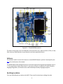
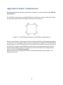
Figure 1.1 shows the MCB1700 board. The board employs a LPC1768, a micro-controller unit
(MCU) made by NXP (affiliated with Philips). There are several input/output peripheral devices
available on the board.
5
Figure 1.1 – The MCB1700 board [2]
The heart of the board is the LPC1768 MCU (microcontroller unit), which contains a CPU, on-chip
flash memory, RAM (Random Access Memory) and some peripheral blocks.
Software
The software used to access the resources on the MCB1700 board is µVision® developed by the
Keil, the manufacturer of the board.
The MCB1700 has been designed mainly to work with high-level programming languages such as
C. The manufacturer clearly states that it is not meant to work as a platform for pure assembly
language! Regardless, the board can be used to develop assembly language programs.
In-lab procedure
First, we will build and run code on the MCU. Then we will review how to debug the code.
6
Running assembly language code on the MCU
Follow the following steps in order to get yourself familiarized with the µVision4 interface.
1 Run the software by clicking on Start/All Programs/Keil µVision4
2 Click on the Project tab, and choose New µVision Project
3 Select or create a subdirectory on N: drive (like N:/ECE_222/Lab_0), then assign a name to
your project (like Lab0 … can be different from folder name), then click on Save DO NOT
MAKE A DIRECTORY, FILE OR PROJECT NAME WITH A SPACE IN IT! A space will prevent
simulation from working properly.
4 To select a CPU, double click on NXP (founded by Philips) and select LPC1768. Click OK
5 Click NO when prompted to copy ‘startup_LPC17xx.s to Project Folder’ which is for C
programmers rather than assembly programmers.
6 Open a web browser and from the lab webpage (http://ece.uwaterloo.ca/~ece222/)
download startup_LPC17xx.s (Assembly startup file) and Lab0_program.s (Sample Lab 0
code). Save them to the Lab_0 folder created in Step #3. When using a web browser, rightclock on the link to the file, and choose ‘Save target as’ to select a destination folder.
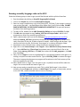
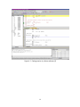
7 Switch back to the uVision4 screen, which should now resemble Figure 1.2.
8 Right click on the Source Group 1 under Target 1. Select Add Files to Group ‘Source Group
1’ … . Select All Files from ‘Files of type’ drop-down menu, which will list all files in the
folder. Select startup_LPC17xx.s, click Add, then select the file Lab0_program.s , click Add
then click Close.
9 Next, click on Target 1 so that it is highlighted (if it is not already) and then click again on it,
waiting a couple of seconds to edit the text. Type in LPC1768_FLASH to rename the target.
The name is appropriate because our program will be written to the Flash memory of the
device as opposed to the RAM.
10 Next, double-click on Target 1 (or click once on the + symbol) to show the files under the
target. Your screen should now match Figure 1.3
11 Now you are ready to assemble your code. This is called ‘Build target’ in the µVision
software. Click on Project tab and then on Build Target. The target, or binary code, written
to the LPC1768, should assemble with no errors or warnings.
7
Figure 1.2 – The µVision4 environment [5]
Figure 1.3 – Building the target [5]
12 The next step is to download the program into the LPC1768. Click on the Flash drop-down
menu and select Download. In order to get the code running, press the Reset button on
the board.
a. If, when downloading the program to the device, you receive a SWD
Communication Failure message, please ensure that you have connected the
device to your workstation via it’s USB cables.
b. To eliminate the need to press the Reset button after every download, right click on
your target, LPC1768_FLASH, and select Options for Target ‘LPC1768_FLASH’ and
then click the Utilities tab. Next click on Settings, select the Use Target Driver for
Flash Programing, click on Flash Download tab, and then ensure the checkbox for
Reset and Run under the Download Function section is selected.
13 You should get an Application running on the message window. Your code is now running!
Using the simulator
The µVision software comes with a powerful Simulator and is used to run code when you do not
have access to an ARM board. Here is how you can switch between debugging on a physical board
and the simulator:
1 Make sure that you are not in the Debug mode. If in Debug mode, simply exit from it by
8
clicking on the Debug button.
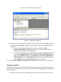
2 Right-click on the LPC1768_FLASH and choose the Options for Target ‘LPC1768_FLASH’
and then click on the Debug tab. You should see Figure 1.4
3 You have the option to choose between the Simulator or the MCB1700 board. If you click
on Use Simulator on the left pane, then you are no longer using the actual board. But if
you choose ULINK2/ME CORTEX DEBUGGER on the right pane, you will need the MCB1700
board connected to the computer you are working on.
Figure 1.4 – Simulator versus MCB1700 board [5]
Debugging assembly language code
As you may have noticed, there is no visual difference on the board when the code is running. So,
how can we make sure that the code is generating the correct results? This is done by running the
code step-by-step and checking the content of registers.
This is called Debug mode. It is a very powerful and useful mode when you want to find a bug in
your code. Your code must generate no errors when assembled before you activate the Debug
mode.
9
The Debug mode can be used both with the Simulator or the board itself. When debugging using
the board, every instruction will be executed on the MCB1700, and the results are communicated
over the ‘ULINK2/ME Cortex Debugger’. Be sure that your workstation is physically connected to
the board via the USB cables, otherwise communication will not be possible.
If Simulator is chosen, then the board is not used at all during the debug mode.
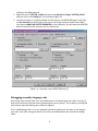
Follow these instructions in order to step through (debug) your code:
1 Make sure you are using the board and not the simulator for the following steps. (see
section Using the Simulator)
2 Choose Start/Stop Debug Session from the Debug drop-down menu.
3 Click OK when presented with the message about being in “Evaluation Mode.” Your
screen should now resemble Figure 1.5
4 Make note of the following important buttons in the graphical user interface (GUI):
From left to right: Reset, Run, Stop, Step, Step Over, Step Out, Run to Cursor Line, Show
Next Statement, Command Window, Disassembly Window, Symbol Window, Registers
Window, Call Stack Window, Watch Windows, Memory Windows, Serial Windows,
Analysis Windows, Trace Windows, System Viewer Windows, Toolbox, Debug Restore
Views
5 Click on the Reset button. The arrow should point to the line LDR R0, =__MAIN
6 Click on the Step button (or F11). The yellow arrow moves down by one line. This
means that the first line was run and you are now about to run the next line
Note: If you experienced difficulty in seeing the yellow arrow in your editor window, an
alternative way to get to the first line of your code is to put a break point in the first instruction
of your code (the first line after the ENTRY), and run the program in the Debug mode. The
program stops in that line.
7 Click on the Step button (or push F11 button on keyboard) several times until you
reach the last line of code (loop B loop) before the END. In each step look at the
register values to make sure that the program is working properly
Lab report
Although there is no mark assigned to this lab, attendance is mandatory and will be checked. You
must complete Lab 0 before starting Lab 1.
10
Figure 1.5 – Debug session in µVision software [5]
11
The assembly language code
;*---------------------------------------------------------------------------;* Name: Lab_0_program.s
;* Purpose: Teaching students how to work with the uVision software
;* Author:
Rasoul Keshavarzi
;*---------------------------------------------------------------------------THUMB
; Thumb instruction set
AREA
My_code, CODE, READONLY
EXPORT
__MAIN
ENTRY
__MAIN
; This name should not be changed. It matches with the startup_LPC17xx.s file.
; Storing 0x1234,5678 into memory address 0x1000,0000 in order to see how little-endian
; approach writes data into memory
MOV
R0, #0x5678 ; Loading least significant part of R0
MOVT
R0, #0x1234 ; Loading most significant part of R0
MOV
R1, #0x0
; Loading least significant part of R1 by zeros
MOVT
R1, #0x1000 ; 0x1000,0000 stored in R1
STR
R0, [R1]
; Look at the memory address 0x1000,0000
; Importing values to registers
MOV
R0, #0x123
MOV
R1, #0x456
MOV
R2, #0x789
MOV
R3, #0xABC
MOV
R4, #0xDEF
MOV
R5, #0x0
; Loading 123 into R0
; Loading 456 into R1
; Loading 789 into R2
; Loading ABC into R3
; Loading DEF into R4
; Loading R5 with zeros
; Swapping the values in R0 and R1 (R5 is used as temporary buffer)
MOV
R5, R0
; R5 <-- R0 (content of R0 is stored in R5)
MOV
R0, R1
; R0 <-- R1 (content of R1 is stored in R0)
MOV
R1, R5
; R1 <-- R5 (content of R5 is stored in R1)
; Adding five values together R5 <-- R0+R1+R2+R3+R4
ADD
R5, R0, R1
; R5 <-- R0 + R1
ADD
R5, R2
; R5 <-- R5 + R2
ADD
R5, R3
; R5 <-- R5 + R3
ADD
R5, R4
; R5 <-- R5 + R4
LOOP
B
LOOP
; Infinite loop
END
12
Lab-1: Flashing LED
Objective
The objective of this lab is to complete, assemble and download a simple assembly language
program. Here is a short list of what you will do in this session:
-
Write some THUMB assembly language instructions
Use different memory addressing modes
Test and debug the code on the Keil board
You will flash an LED (Light Emitting Diode) at an approximate 1 Hz frequency.
Background
The LPC1768 belongs to the Cortex-M3 family of microprocessors which uses the THUMB
instruction set. Thumb is a subset of the ARM instruction set.
In order to flash an LED, one needs to know how the LPC1768 microprocessor is connected to the
LEDs – the pin configuration and interfacing. A lot of the hardware interfacing details are in Lab-3.
The details to accomplish this lab are:
-
Writing 0xB0000000 into memory address 0x2009C020 turns “off” the three LEDs on port 1
(pins P1.28, P1.29, and P1.31)
Writing 0x0000007C into memory address 0x2009C040 turns “off” the five LEDs on port 2
(pins P2.2 to P2.6)
Toggling bit 28 of the address 0x2009C020 will cause the corresponding LED (P1.28) to
alternate between “on” and “off”. The memory address is 32 bits wide (bit 31 down to bit
0). You should switch between 0xB0000000 and 0xA0000000 to flash the LED.
Pre-lab
Before the lab session, look at the THUMB instruction set in Appendix B. The LPC1768 is a CortexM3 ARM CPU using the THUMB instructions set.
In order to see a flashing LED, implement a delay between the LED “on” and “off” states. Think
about implementing a delay in assembly language.
Hint: Increment or decrement a register in a loop until it reaches a certain value.
There is no deliverable as pre-lab for this lab.
13
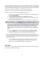
In-lab procedure
Complete the given code that is mostly written.
-
-
Create a new folder (like N:\ECE222\Lab1) and project as was done in Lab-0
Start by turning off all eight LEDs
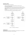
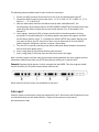
Then implement the flashing LED code using an infinite loop which toggles bit 28 of the
address 0x2009C020. Figure 1.1 shows the two different approaches. The shorter flowchart
leads to smaller code size and the longer flowchart will cost you marks as the code is
inefficient!
Don’t forget to insert a 500mS delay in the loop; otherwise it is too fast to see.
Assemble the code, download it to the board, and debug it if necessary.
Figure 1.1 – Flowcharts for flashing LED
Coding Goals
All code should be well commented. All code added to an existing program, for a lab, should be
identified. Ideally ALL documentation is within the program.
14
Lab report
Submit a report in CourseBook. To understand the deliverables look at the Lab-1 Submission form.
The assembly language code
;*---------------------------------------------------------------------------;* Name: Lab_1_program.s
;* Purpose: This code flashes one LED at approximately 1 Hz frequency
;* Author:
Rasoul Keshavarzi
;*----------------------------------------------------------------------------*/
THUMB
; Declare THUMB instruction set
AREA
My_code, CODE, READONLY ;
EXPORT
__MAIN
; Label __MAIN is used externally q
ENTRY
__MAIN
; The following operations can be done in simpler methods. They are done in this
; way to practice different memory addressing methods.
; MOV moves into the lower word (16 bits) and clears the upper word
; MOVT moves into the upper word
; show several ways to create an address – using a fixed offset and register as offset
; and several examples are used below
; NOTE MOV can move ANY 16-bit, and only SOME >16-bit, constants into a register
MOV
R2, #0xC000
; move 0xC000 into R2
MOV
R3, #0xB0000000
; move initial Port 1 value into R3
MOV
R4, #0x0
; init R4 register to 0 to build address
MOVT
R4, #0x2009
; assign 0x20090000 into R4
ADD
R4, R4, R2
; add 0xC000 to R4 to get 0x2009C000
STR
R3, [r4, #0x20]
; Turn off three LEDs on Port 1 using an offset
MOV
R3, #0x0000007C
; move initial value for port P2
STR
R3, [R4, #0x40]
; Turn off five LEDs on port 2
MOV
R2, #0x20
; put Port 1 offset into R2
MOV
R0, #0xFFFF
; Initialize R0 lower word for countdown
loop
SUBS
R0, #1
; Decrement r0 and set N,Z,V,C status bits
;
;
Approximately five lines of code
;
are required to complete the program
;
STR
R3, [R4, R2]
; Toggle the bit 28 or port 1
B
loop
; This branch needs to be fixed!
END
15
Lab-1 Submission form
Class: 001 □
002 □
201 □
204 □
202 □
205 □
203 □
206 □
Demo date:
Submission Statement: We (I) are (am) submitting this report for grading in ECE 222. We (I) certify that this
report (including any code, descriptions, flowcharts, etc., that are part of the submission) were written by us (me) and
have received no prior academic credit at this university or any other institution. The penalty for copying or
plagiarism will be a grade of zero (0).
Member 1
Member 2
Name:
Name:
UW-ID (NOT student #)
UW-ID (NOT student #)
Signature:
Signature:
Note: Reports submitted without a signed submission statement will receive a grade of zero (0).
Part-I
Part-II
Lab-demo
Part-III
Lab report
Pre-lab
Lab completion
Questions
Code quality
Code comments
Total
Weight
0
30
30
20
20
Grade
Comment
--
100
16
Lab-2: Subroutines and parameter passing
Objective
In structured programming, big tasks are broken into small routines. A short program is written for
each routine. The main program brings the subroutines together by calling them.
In most cases when a subroutine is called, some information, parameters, must be communicated
between the main program and the subroutine. This is called parameter passing.
In this lab, you will practice subroutine calling and parameter passing by implementing a Morse
code system.
What you do
In this lab you will turn one LED into a Morse code transmitter. You will cause one LED to blink in
Morse code for a four character word.
Pre-lab
Think about implementing Lab-1 code using subroutines. Write a subroutine called LED_OFF that
turns LED P.1.28 off, and another subroutine called LED_ON that turns the LED on. Write a third
subroutine called DELAY that takes one input parameter (register R0) and waits for R0 * 500ms
before returning.
Submit the subroutines, as a single text file, to the electronic drop-box as Prelab-2.
Hints
The Course Notes have excellent code examples for subroutine and pass-by-stack.
Optimization can be done to greatly reduce the size of the assembly code. This should not be
attempted until everything is working and only if the student has time. Lab-2 can be done in 150
lines of code with the main loop taking around 40 lines. Expect to add a good fraction of your
code size in comments before submission for marking.
Simulate to check the basic operation before downloading to hardware! To simulate the code use
breakpoints or comment out the branch instruction in the timing loop so that it passes thru .
Data can be passed to a subroutine via the registers, stack or memory. Passing by memory
requires the programmer to organize how the memory is used. Passing by register is the easiest
17
but there are a limited number of registers to use. Passing by stack is the most flexible, however it
is the most complex and error prone method for assembly language programmers. When starting
with subroutines use only register passing. When your code is working switch one subroutine to
using pass-by-stack.
Here is an example of a subroutine using pass-by-register. In this example the STMFD instruction
stores registers onto the stack. R14 is the Link Register and holds the address to return to. R14 is
pushed on the stack and then all registers are restored, just before exit, with the LDMFD
instruction. A twist is that the return address is restored to R15, the Program Counter, so that the
next instruction executed is the one after “BL
mySubroutine”. Some programs may be
expecting a “RTS” or Return To Sender instruction to mark the end of the subroutine but it is not
used with ARM.
ADD ….
MOV
BL
MOV ….
…
R2, #0x20
mySubroutine
; some code
; put some data into R2 for the subroutine
; branch and link to “mySubroutine”
; more code
mySubroutine
STMFD
R13!, {R0, R2-R4, R14} ; save R0, R2 to R4 and R14 on the stack, R14 is the
address to return to
MOV
R3, #0x0000007C
ADD
R3, R3, R2
; do something
LDMFD
R13!, {R0, R2-R4, R15} ; restore R0, R2 to R4 and put the return address that
was in R14 into R15 the program counter
To pass data into a subroutine using the stack, before the subroutine call the data must be put
onto the stack. The programmer must calculate how much is pushed onto the stack at the start of
the subroutine and use that as an offset. An example is below. A different example is in the
course text and course notes and it offers advantages and also demonstrates passing data back.
ADD ….
STR
STR
ABC
BL
ADD
; some code
R0, [R13, #-4]!
; push R0 value onto the stack (taking 4 bytes)
R3, [R13, #-4]!
; push R3 value onto the stack
; code which destroys what was in R0 and R3
mySubroutine
; branch and link to “mySubroutine”
R13, R13, #8
; pop the 8 bytes of data (R0, R3) put onto the stack
MOV ….
…
; more code
18
mySubroutine
STMFD
R13!, {R0, R4, R14} ; push R0, R4 and R14 taking 3 x 4 = 12 bytes
; To read from the stack offset 12 bytes for pushed registers and then 4 bytes per data
LDR
R0, [R13, #12]
; read the value of R3 that was pushed onto the stack
LDR
R4, [R13, #16]
; read the value of R0 that was pushed onto the stack
ADD
LDMFD
R3, R3, R2
R13!, {R0, R4, R15}
; rest of the subroutine till return with LDMFD ….
; restore R0, R4 and the return address
Lookup Tables
Creating a lookup table is very easy. However, one must be careful as to how one reads it and
indexes into it. Data can be 8-bit (byte), 16-bit (half-word) or 32-bit (word). The ARM
documentation may confuse you if you are used to calling 16-bit a word and 32-bit a long word.
Here is some simple code to loop thru data in a lookup table:
ADD ….
ResetLUT
; some code
LDR
R5, =LUT
LDRD R6, [R5]
TEQ R6, #0
BEQ ResetLUT
ADD
R5, #4
DDD
LUT
ALIGN
DCD
; assign the address for the lab LUT to R5
; read the first 32-bit word from the LUT
; test it to see if we hit the null at the end
; If we hit the end, start at the beginning of the LUT
; add 4 (bytes) to point to the next 32-bit data in LUT
; R6 now holds the data read from the LUT
; more code to do something with the data from the LUT
; make sure that the data is aligned properly in memory
469, 0x020, 3, 5, 0x3F2, 0
; LookUp Table with a null or 0 to mark the end
In order to work with 16-bit data the LUT has to be type DCW, you have to increment by 2 (bytes)
to move thru the data and to read the table you need to use LDRH. For Bytes use DCB and LDRB.
In-lab procedure
Implement the following changes to the provided, or your Lab-1, code:
1.
2.
3.
4.
5.
Put the initials of the two lab partners into a lookup tabled called InputLUT
Turn all LEDs off
Add the subroutines LED_OFF and LED_ON to turn off, and on, LED P.1.28
Call the subroutine DELAY between calls to LED_OFF and LED_ON to test all three
Then write a subroutine called CHAR2MORSE that converts an ASCII character in R0 into a
Morse code pattern in R1
19
The following steps should be done for each of the four characters:
1 Extract one ASCII character (from the first to last) from the lookup table InputLUT
2 Convert the ASCII character to an index value . Ie “A” or 0x41 is 0, “B” or 0x42 is 1, “C” or
0x43 is 2, …, “Z” or 0x5A is 25
3 With the index value read from the Morse look-up table, called MorseLUT, the
corresponding, 16-bit, Morse pattern. BE VERY CAREFUL DOING THIS! Carefully match your
index value (an offset in bytes) with the size of the data (8, 16 or 32-bits wide) in the
MorseLUT.
4 Use a register, starting at 0xF0, to keep track which bit of the Morse pattern is being
processed. To remove leading 0’s in the Morse pattern decrement the register and shiftleft the Morse pattern until a ‘1’ is read (do this add this AFTER your code is working; you
may want to look at the CLZ instruction). Note: one can determine if all of the Morse
pattern has been shifted out, without a counter, several ways.
5 Turn the LED on and off according to the Morse code (with delays between consecutive
bits) for that letter down to bit 0
6 Insert a long delay (3 dots) before fetching next character
7 Insert a long delay (7 dots) and show the same four letters over again
Note: Use both registers and the stack for parameter passing between the main program and the
subroutines. Add pass-by-stack only AFTER everything is working as it’s harder to do.
Example: Suppose the lab partner’s initials compose the word BIRD. Then the program should
extract the letters (B I R D) and create a Morse code like this:
Please note that all four letters are considered as one word.
Lab report
Submit a report to the electronic drop-box prepared for lab-2. Examine the Lab-2 Submission form
to understand what you will need to deliver. Expect to have nearly as many lines of
documentation as code.
20
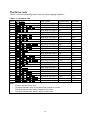
The Morse code
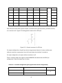
Table 2.1 shows corresponding Morse codes for English language alphabets:
Table 2.1 – The Morse code
Letter Morse code
Binary value
Decimal value
A
0000,0000,0001,0111 23
B
0000,0001,1101,0101 469
C
0000,0111,0101,1101 1885
D
0000,0000,0111,0101 117
E
0000,0000,0000,0001 1
F
0000,0001,0101,1101 349
G
0000,0001,1101,1101 477
H
0000,0000,0101,0101 85
I
0000,0000,0000,0101 5
J
0001,0111,0111,0111 6007
K
0000,0001,1101,0111 471
L
0000,0001,0111,0101 373
M
0000,0000,0111,0111 119
N
0000,0000,0001,1101 29
O
0000,0111,0111,0111 1911
P
0000,0101,1101,1101 1501
Q
0001,1101,1101,0111 7639
R
0000,0000,0101,1101 93
S
0000,0000,0001,0101 21
T
0000,0000,0000,0111 7
U
0000,0000,0101,0111 87
V
0000,0001,0101,0111 343
W
0000,0001,0111,0111 375
X
0000,0111,0101,0111 1879
Y
0001,1101,0111,0111 7543
Z
0000,0111,0111,0101 1909
Notes:
- A dash is equal to three dots
- The space between parts of the same letter is equal to one dot
- The space between two letters is equal to three dots
- The space between two words is equal to seven dots
21
Hex value
17
1D5
75D
75
1
15D
1DD
55
5
1777
1D7
175
77
1D
777
5DD
1DD7
5D
15
7
57
157
177
757
1D77
775
Lab-2 Submission form
201 □
204 □
202 □
205 □
203 □
206 □
Demo date:
Submission Statement: We (I) are (am) submitting this report for grading in ECE 222. We (I) certify that this
report (including any code, descriptions, flowcharts, etc., that are part of the submission) were written by us (me) and
have received no prior academic credit at this university or any other institution. The penalty for copying or
plagiarism will be a grade of zero (0).
Member 1
Member 2
Name:
Name:
UW-ID (NOT student #)
UW-ID (NOT student #)
Signature:
Signature:
Note: Reports submitted without a signed submission statement will receive a grade of zero (0).
Part-I
Part-II
Lab-demo
Part-III
Lab report
Pre-lab
Lab completion
Questions
Code quality
Code comments
Total
Weight
10
30
30
20
10
Grade
100
22
Comment
Lab-3: Input/Output Interfacing
Objective
The objective of this lab is to learn how to use peripherals connected to a microprocessor. The
ARM CPU is connected to the outside world using Ports and in this lab you will setup, and use,
Input and Output ports.
What you do
In this lab you will measure how fast a user responds to an event accurate to a 10th of a
millisecond. Initially all LEDs are off and after a random amount of time (between 2 to 10
seconds), one LED turns on and then the user presses the push button.
Between ‘Turning the LED on’ and ‘Pressing the push button’, a 32 bit counter is incremented
every 10th of a millisecond in a loop. The final value of this 32 bit number should be sent to the 8
LEDs in separate bytes with a 2 second delay between them.
Background
You will need to review the information presented in the schematic diagram (Appendix F) as well
as the LPC17xx User manual [1] (literature number UM10360). Information about the LEDs and
INT0 push button is in the Appendix D.
Pre-lab
In Lab 1 and 2 the method used to turn the LEDs on and off was very strange as the IO pins were
changed from input to output in order to turn an LED off or on! The FIODIR address was used
instead of writing 0’s and 1’s to the outputs (FIOPIN).
Before the lab determine what to write into which memory-address to turn any of the 8 LEDs on
or off. Refer to Appendix D or the LPC17xx User manual [1].
The INT0 push button is also used. It should be set to an input GPIO type port with a pull-up
resistor. Note that this is done by default.
Submit assembly language code for the following tasks to the drop-box for Prelab-3:
-
Subroutine which implements a 100uS delay.
23
-
-
Pseudo or asm. code that initializes the INT0 button as GPIO port with a pull-up resistor.
PINSEL3 and PINSEL4 addresses are defined in the sample code. The default value is 0x0 so
one just has to set the appropriate bits. INT0 is pin P2.10
Pseudo or asm. code that displays the lowest 8-bits of R0 on the 8 LEDs
Calculate the number of 100uS delay routine loops that are necessary to generate the time
delays required (0.1, 0.25, 2, 5 seconds).
In-lab procedure
Here are the steps to implement this program:
1. Verify your timing loop which generates a 100uS delay by looping it to get a 10 second
delay.
2. Create a simple counter to generate numbers from 0 to 255 (0xff) and write these to the 8
LEDs to verify this functionality using a 0.25 second delay between numbers.
3. Add the random number routine and display the 8-bit output to the LEDs to verify the
operation of the random number generator.
4. To implement the project:
1. Implement a loop with 0.1 second delay between generating a random number and
displaying it on the LEDs until INT0 is pressed at the start of the program.
2. Call the given random-number function to generate a number and add an offset to
get a number to generate a delay between 2 to 10 seconds and then delay that
long. You may use as many of the 16-bits of the pseudo-random number as you
wish BUT using only the least signif. 3 bits will not give a good result. Use 8 bits or
more and scale the result to get what you need.
3. Turn one LED on and start counting 10th’s of millisecond time periods (100uS each)
4. With polling, monitor the status of the INT0 push button
5. Once the button is pushed, stop incrementing (exit from the loop)
6. Send the first 8 bits (least significant part) of the register to the LEDs
7. Wait for two seconds (pressing INT0 should cause an exit)
8. Send the next 8 bits, wait 5 seconds and go back to step 8. WHENEVER the INT0
button is pushed reset the time-delay counter and go to step 2.
5. With everything working, add your code to set the INT0 button as a GPIO input port with
pull-up.
Lab report
Submit a report to the electronic drop-box prepared for Lab-3. Take a look at the Lab-3 Submission
form to understand what you will need to deliver.
Answer these questions and put them as comments at the end of your program:
24
If a 32-bit register is counting the number of 10th’s of milliseconds, what is the maximum amount
of time which can be encoded in 8 bits, 16-bits, 24-bits and 32-bits?
Considering the question above could the program be improved by displaying 16-bits or 24-bits or
by reducing the timing loop to 10us delay time or increasing it to 1ms? Consider: What is a typical
reaction time? How consistent is a person?
Extra Information
Random numbers with linear feedback shift registers at WikiPedia:
http://en.wikipedia.org/wiki/Linear_feedback_shift_register
25
Lab-3 Submission form
201 □
204 □
202 □
205 □
203 □
206 □
Demo date:
Submission Statement: We (I) are (am) submitting this report for grading in ECE 222. We (I) certify that this
report (including any code, descriptions, flowcharts, etc., that are part of the submission) were written by us (me) and
have received no prior academic credit at this university or any other institution. The penalty for copying or
plagiarism will be a grade of zero (0).
Member 1
Member 2
Name:
Name:
UW-ID (NOT student #)
UW-ID (NOT student #)
Signature:
Signature:
Note: Reports submitted without a signed submission statement will receive a grade of zero (0).
Part-I
Part-II
Lab-demo
Part-III
Lab report
Pre-lab
Lab completion
Questions
Code quality
Code comments
Total
Weight
10
30
30
20
10
Grade
100
26
Comment
Lab-4: Interrupt Handling
Objective
The objective of this lab is to learn about interrupts. You will enable an interrupt source in the
LPC1768 microprocessor, and you will write an interrupt service routine (ISR) that is triggered
when pressing the INT0 button. The ISR will return to the main program after handling the
interrupt.
What to do
The objectives for Lab-4 are achieved by implementing a program similar to the program for Lab-3,
except using interrupt-drive I/O instead of programmed I/O.
Pre-lab
Identify all relevant I/O register memory addresses (see the UM10360 manual). Write an initial
program that configures the pin control block (i.e., setting the function of pins to GPIO, setting the
direction to either input or input), and that enables GPIO interrupts sensitive to the falling edge of
P2.10 (the INT0 button). Take a look at the EINT3_IRQHandler code in the start-up file and set a
breakpoint in it. Test your initial program by ensuring that program execution jumps to the
interrupt handler when pressing the INT0 button. Be sure to clear the interrupt.
In-lab procedure
NOTE: In the past we’ve polled on a global flag which indicates that the interrupt was received.
This new method avoids the global flag nicely.
The following is a high-level description of the program you will implement:
You will implement a “random countdown timer.”
Your main program will run an infinite loop in which the LED displays the current number in R10.
The main program can be interrupted by the user pressing the INT0 button. When this occurs, an
interrupt service routine will generate a new random number, which is then displayed using the
LEDs. Each number flashes on for a half second, then off for a half second. The number is
decremented by 1 every second.
The program begins with the LEDs turned off. The random 8-bit number will be displayed in binary
using the LEDs. If a light is ON, then it represents a 1; if a light is OFF, then it represents a 0. The
most significant bit will correspond with the leftmost LED.
You are provided with a template that gives you an idea of how to organize your code. Carefully
read the comments in the source files. There are four subroutines that you will be using:
27
1. STORE_NUM
a. This subroutine will parse out the last eight bits stored in R10, and will store these
bits appropriately in R3 and R4.
b. R3 saves the least significant bits, and R4 saves the most significant bits (of the 8-bit
number)
HINT: The DISPLAY_NUM subroutine will be called after STORE_NUM.
DISPLAY_NUM uses R3 to write to FIO2SET register, which will turn on the
appropriate LEDs for P2.2 thru P2.6, and it uses R4 to write to the FIO1SET
register, which will turn on the appropriate LEDs for P1.28, P1.29, and P1.31.
Thus, when parsing out the 8-bits, pay close attention to which bits in R3
and R4 should be turned on in order to display the correct LEDs. Keep in
mind both the order and locations of the bits.
2. DISPLAY_NUM
a. This subroutine uses R3 and R4 to turn on the appropriate LEDs. STORE_NUM
should be called prior to calling this subroutine. See above hint.
3. RandomNum
a. Same as Lab 3.
4. DELAY
a. This should cause a delay of R0 x 0.5 seconds.
(Note that registers R10 and R11 both have a specific purpose: R10 will always store the current
number being displayed by the LEDs; R11 will contain the most recently generated random
number.)
Additionally, you will write an interrupt service routine called EINT3_IRQHandler, which is actually
located in the startup_LPC17xx.s file. An updated version of the start-up file is provided for this
lab. Open this file and scroll down until you find the EINT3_IRQHandler label. You need to
implement it as follows:
Clear the interrupt (register IO2IntClr) for P2.10 (remember that pin 10 corresponds with
the 11th bit of the register)
Call RandomNum, which stores a new random number in R11. Store this number in R10.
Call STORE_NUM, which parses out the last 8-bits of R10 and stores these bits
appropriately in R3 and R4. (Doing this in the ISR ensures that the next number flashed
using the LEDs will be the new number.)
Lab report
Submit a report to the Lab-4 drop-box. Look at the Lab-4 Submission form for the deliverables.
28
Lab-4 Submission form
201 □
204 □
202 □
205 □
203 □
206 □
Demo date:
Submission Statement: We (I) are (am) submitting this report for grading in ECE 222. We (I) certify that this
report (including any code, descriptions, flowcharts, etc., that are part of the submission) were written by us (me) and
have received no prior academic credit at this university or any other institution. The penalty for copying or
plagiarism will be a grade of zero (0).
Member 1
Member 2
Name:
Name:
UW-ID (NOT student #)
UW-ID (NOT student #)
Signature:
Signature:
Note: Reports submitted without a signed submission statement will receive a grade of zero (0).
Part-I
Part-II
Lab-demo
Part-III
Lab report
Pre-lab
Lab completion
Questions
Code quality
Code comments
Total
Weight
10
30
30
20
10
Grade
100
29
Comment
Appendix A: The LPC1768 microprocessor
Figure A.1 shows block diagram of the LPC1768. Detailed information can be found in chapter 1 of
the document LPC17xx User manual [1].
Figure A.1 – Block diagram of LPC1768 [1]
Figure A.2 shows a simplified block diagram of the LPC1768 microprocessor.
As you can see there is no memory block in the above figure. This is because all volatile (RAM) and
non-volatile (Flash) memories are on-chip.
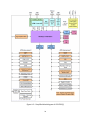
Figure A.3 shows some details of the CPU and buses.
30
Figure A.2 – Simplified block diagram of LPC1768 [1]
31
Figure A.3 – LPC1768 block diagram, CPU, and buses [1]
32
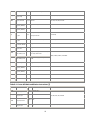
Appendix B: Instruction Set Summary
The processor implements a version of the Thumb instruction set. Table B.1 lists the supported
instructions [7]. Details on the instructions can be found at:
http://infocenter.arm.com/help/topic/com.arm.doc.dui0204j/Cihedhif.html
Note for the tables:
angle brackets, <>, enclose alternative forms of the operand
braces, {}, enclose optional operands
the Operands column is not exhaustive
Op2 is a flexible second operand that can be either a register or a constant
most instructions can use an optional condition code suffix.
Most instructions support the suffix “S”, which will result in flags being set
Status Flags set include: Negative, Zero, Carry, oVerflow
For more information on the instructions and operands, see the instruction descriptions.
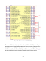
Table B.1. Cortex-M3 Instructions [7]
Mnemonic
ADC{S}
ADD{S}
ADD,
ADDW
ADR
AND{S}
ASR{S}
B
BFC
BFI
BIC{S}
BKPT
Operands
{Rd,} Rn, Op2
{Rd,} Rn, Op2
{Rd,} Rn, #imm12
Rd, label
{Rd,} Rn, Op2
Rd, Rm, <Rs|#n>
label
Rd, #lsb, #width
Rd, Rn, #lsb, #width
{Rd,} Rn, Op2
#imm
Flags
Brief description
See
N,Z,C,V Add with Carry
N,Z,C,V Add
ADD, ADC, SUB, SBC, and RSB
N,Z,C,V Add
-
Load PC-relative Address
ADR
N,Z,C
Logical AND
AND, ORR, EOR, BIC, and ORN
N,Z,C
Arithmetic Shift Right
ASR, LSL, LSR, ROR, and RRX
-
Branch: BEQ (Equal 0), BNE (Not zero),
BCC (carry clear), BCS (carry set), etc
B, BL, BX, and BLX
-
Bit Field Clear
BFC and BFI
-
Bit Field Insert
BFC and BFI
N,Z,C
Bit Clear
AND, ORR, EOR, BIC, and ORN
-
Breakpoint
BKPT
33
Mnemonic
BL
BLX
BX
CBNZ
CBZ
CLREX
CLZ
CMN
CMP
CPSID
CPSIE
EOR{S}
Operands
label
Rm
Rm
Rn, label
Rn, label
-
Rd, Rm
Rn, Op2
Rn, Op2
i
i
{Rd,} Rn, Op2
LDM
Rn{!}, reglist
LDMDB,
LDMEA
Rn{!}, reglist
LDMFD,
LDMIA
Rn{!}, reglist
LDR
LDRB,
LDRBT
LDRD
LDREX
LDREXB
LDREXH
LDRH,
Rt, [Rn, #offset]
Flags
Brief description
See
-
Branch with Link
-
Branch indirect with Link
-
Branch indirect
-
Compare and Branch if Non Zero
-
Compare and Branch if Zero
-
Clear Exclusive
-
Count Leading Zeros
B, BL, BX, and BLX
N,Z,C,V Compare Negative, eval Rn+Op2
N,Z,C,V Compare, evaluates Rn – Op2
-
Change Processor State, Disable
Interrupts
CPS
-
Change Processor State, Enable
Interrupts
CPS
N,Z,C
Exclusive OR
AND, ORR, EOR, BIC, and ORN
-
Load Multiple registers, increment after
-
Load Multiple registers, decrement
before
-
Load Multiple registers, increment after
-
Load Register with 32-bit word
-
Load Register with byte
-
Load Register with two bytes
-
Load Register Exclusive
-
Load Register Exclusive with Byte
-
Load Register Exclusive with Halfword
-
Load Register with Halfword
LDM and STM
Memory access instructions
Rt, [Rn, #offset]
Rt, Rt2, [Rn, #offset]
Rt, [Rn, #offset]
Rt, [Rn]
Rt, [Rn]
Rt, [Rn, #offset]
LDR and STR, immediate offset
LDREX and STREX
Memory access instructions
34
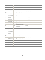
Mnemonic
Operands
Flags
Brief description
See
LDRHT
LDRSB,
LDRSBT
Rt, [Rn, #offset]
LDRSH,
LDRSHT
Rt, [Rn, #offset]
LDRT
LSL{S}
LSR{S}
MLA
MLS
MOV{S}
MOVT
MOVW,
MOV
MUL{S}
MVN{S}
NOP
ORN{S}
Rt, [Rn, #offset]
Rd, Rm, <Rs|#n>
Rd, Rm, <Rs|#n>
Rd, Rn, Rm, Ra
Rd, Rn, Rm, Ra
Rd, Op2
Rd, #imm16
Rd, #imm16
{Rd,} Rn, Rm
Rd, Op2
{Rd,} Rn, Op2
-
Load Register with Signed Byte
-
Load Register with Signed Halfword
-
Load Register with word
N,Z,C
Logical Shift Left
N,Z,C
Logical Shift Right
-
Multiply with Accumulate, 32-bit result
-
Multiply and Subtract, 32-bit result
N,Z,C
Move
MOV and MVN
-
Move Top
MOVT
N,Z,C
Move 16-bit constant, top word set to
zero
MOV and MVN
N,Z
Multiply, 32-bit result
MUL, MLA, and MLS
N,Z,C
Move NOT
MOV and MVN
-
No Operation
NOP
N,Z,C
Logical OR NOT
N,Z,C
Logical OR
-
Pop registers from stack
-
Push registers onto stack
-
Reverse Bits
-
Reverse byte order in a word
-
Reverse byte order in each halfword
-
Reverse byte order in bottom halfword
and sign extend
ASR, LSL, LSR, ROR, and RRX
MUL, MLA, and MLS
AND, ORR, EOR, BIC, and ORN
ORR{S}
POP
PUSH
RBIT
REV
REV16
REVSH
{Rd,} Rn, Op2
reglist
reglist
Rd, Rn
Rd, Rn
Rd, Rn
Rd, Rn
PUSH and POP
35
REV, REV16, REVSH, and RBIT
Mnemonic
ROR{S}
RRX{S}
RSB{S}
SBC{S}
SBFX
SDIV
SEV
SMLAL
SMULL
SSAT
STM
Operands
Rd, Rm, <Rs|#n>
Rd, Rm
{Rd,} Rn, Op2
{Rd,} Rn, Op2
Rd, Rn, #lsb, #width
{Rd,} Rn, Rm
RdLo, RdHi, Rn, Rm
RdLo, RdHi, Rn, Rm
Rd, #n, Rm {,shift
#s}
Rn{!}, reglist
STMDB,
STMEA
Rn{!}, reglist
STMFD,
STMIA
Rn{!}, reglist
STR
STRB,
STRBT
STRD
STREX
STREXB
STREXH
STRH,
STRHT
STRT
Rt, [Rn, #offset]
Flags
Brief description
N,Z,C
Rotate Right
N,Z,C
Rotate Right with Extend
See
ASR, LSL, LSR, ROR, and RRX
N,Z,C,V Reverse Subtract
N,Z,C,V Subtract with Carry
-
Signed Bit Field Extract
SBFX and rUBFX
-
Signed Divide
SDIV and UDIV
-
Send Event
SEV
-
Signed Multiply with Accumulate (32 x
32 + 64), 64-bit result
-
Signed Multiply (32 x 32), 64-bit result
Q
Signed Saturate
-
Store Multiple registers, increment
after
-
Store Multiple registers, decrement
before
-
Store Multiple registers, increment
after
-
Store Register word
-
Store Register byte
-
Store Register two words
-
Store Register Exclusive
-
Store Register Exclusive Byte
-
Store Register Exclusive Halfword
-
Store Register Halfword
UMULL, UMLAL, SMULL, and SMLAL
SSAT and USAT
LDM and STM
Memory access instructions
Rt, [Rn, #offset]
Rt, Rt2, [Rn, #offset]
Rd, Rt, [Rn, #offset]
Rd, Rt, [Rn]
Rd, Rt, [Rn]
Rt, [Rn, #offset]
Rt, [Rn, #offset]
LDR and STR, immediate offset
LDREX and STREX
Memory access instructions
-
Store Register word
36
Mnemonic
SUB{S}
SUB,
SUBW
SXTB
SXTH
Operands
{Rd,} Rn, Op2
{Rd,} Rn, #imm12
{Rd,} Rm {,ROR #n}
{Rd,} Rm {,ROR #n}
Flags
Brief description
See
N,Z,C,V Subtract
ADD, ADC, SUB, SBC, and RSB
N,Z,C,V Subtract
ADD, ADC, SUB, SBC, and RSB
-
Sign extend a byte
SXT and UXT
-
Sign extend a halfword
SXT and UXT
Test Equivalence, same as EORS
TEQ
TST
UBFX
UDIV
UMLAL
Rn, Op2
Rn, Op2
Rd, Rn, #lsb, #width
{Rd,} Rn, Rm
RdLo, RdHi, Rn, Rm
N,Z,C
TST and TEQ
but it preserves Rn
N,Z,C
Test, same as ANDS but it preserves Rn TST and TEQ
-
Unsigned Bit Field Extract
SBFX and UBFX
-
Unsigned Divide
SDIV and UDIV
-
Unsigned Multiply with Accumulate (32
x 32 + 64), 64-bit result
-
Unsigned Multiply (32 x 32), 64-bit
result
Q
Unsigned Saturate
SSAT and USAT
-
Zero extend a Byte
SXT and UXT
-
Zero extend a Halfword
SXT and UXT
-
Wait For Event
WFE
-
Wait For Interrupt
WFI
UMULL, UMLAL, SMULL, and SMLAL
UMULL
USAT
UXTB
UXTH
WFE
WFI
RdLo, RdHi, Rn, Rm
Rd, #n, Rm {,shift
#s}
{Rd,} Rm {,ROR #n}
{Rd,} Rm {,ROR #n}
-
Table B.1. Cortex-M3 Math and Bitwise Instructions [7]
Mnemonic
ADC{S}
ADD{S}
ADD,
ADDW
AND{S}
Operands
{Rd,} Rn, Op2
{Rd,} Rn, Op2
{Rd,} Rn, #imm12
{Rd,} Rn, Op2
Flags
Brief description
See
N,Z,C,V Add with Carry
N,Z,C,V Add
ADD, ADC, SUB, SBC, and RSB
N,Z,C,V Add
N,Z,C
Logical AND
AND, ORR, EOR, BIC, and ORN
37
Mnemonic
ASR{S}
BFC
BFI
BIC{S}
CLZ
EOR{S}
LSL{S}
LSR{S}
MLA
MLS
MUL{S}
ORN{S}
Operands
Rd, Rm, <Rs|#n>
Rd, #lsb, #width
Rd, Rn, #lsb, #width
{Rd,} Rn, Op2
Rd, Rm
{Rd,} Rn, Op2
Rd, Rm, <Rs|#n>
Rd, Rm, <Rs|#n>
Rd, Rn, Rm, Ra
Rd, Rn, Rm, Ra
{Rd,} Rn, Rm
{Rd,} Rn, Op2
Flags
Brief description
See
N,Z,C
Arithmetic Shift Right
ASR, LSL, LSR, ROR, and RRX
-
Bit Field Clear
BFC and BFI
-
Bit Field Insert
BFC and BFI
N,Z,C
Bit Clear
AND, ORR, EOR, BIC, and ORN
-
Count Leading Zeros
N,Z,C
Exclusive OR
N,Z,C
Logical Shift Left
AND, ORR, EOR, BIC, and ORN
ASR, LSL, LSR, ROR, and RRX
N,Z,C
Logical Shift Right
-
Multiply with Accumulate, 32-bit
result
-
Multiply and Subtract, 32-bit result
N,Z
Multiply, 32-bit result
N,Z,C
Logical OR NOT
N,Z,C
Logical OR
-
Reverse Bits
-
Reverse byte order in a word
-
Reverse byte order in each
halfword
-
Reverse byte order in bottom
halfword and sign extend
N,Z,C
Rotate Right
N,Z,C
Rotate Right with Extend
MUL, MLA, and MLS
MUL, MLA, and MLS
AND, ORR, EOR, BIC, and ORN
ORR{S}
RBIT
REV
REV16
REVSH
ROR{S}
RRX{S}
RSB{S}
SBC{S}
SBFX
{Rd,} Rn, Op2
Rd, Rn
Rd, Rn
Rd, Rn
Rd, Rn
Rd, Rm, <Rs|#n>
Rd, Rm
{Rd,} Rn, Op2
{Rd,} Rn, Op2
Rd, Rn, #lsb, #width
REV, REV16, REVSH, and RBIT
ASR, LSL, LSR, ROR, and RRX
N,Z,C,V Reverse Subtract
N,Z,C,V Subtract with Carry
-
Signed Bit Field Extract
SBFX and rUBFX
38
Mnemonic
SDIV
SMLAL
Operands
{Rd,} Rn, Rm
RdLo, RdHi, Rn, Rm
Flags
Brief description
-
Signed Divide
-
Signed Multiply with Accumulate
(32 x 32 + 64), 64-bit result
-
Signed Multiply (32 x 32), 64-bit
result
Q
Signed Saturate
See
SDIV and UDIV
UMULL, UMLAL, SMULL, and SMLAL
SMULL
SSAT
SUB{S}
SUB, SUBW
SXTB
SXTH
RdLo, RdHi, Rn, Rm
Rd, #n, Rm {,shift #s}
{Rd,} Rn, Op2
{Rd,} Rn, #imm12
{Rd,} Rm {,ROR #n}
{Rd,} Rm {,ROR #n}
SSAT and USAT
N,Z,C,V Subtract
ADD, ADC, SUB, SBC, and RSB
N,Z,C,V Subtract
ADD, ADC, SUB, SBC, and RSB
-
Sign extend a byte
SXT and UXT
-
Sign extend a halfword
SXT and UXT
Test Equivalence, same as EORS
TEQ
TST
UBFX
UDIV
UMLAL
Rn, Op2
Rn, Op2
Rd, Rn, #lsb, #width
{Rd,} Rn, Rm
RdLo, RdHi, Rn, Rm
N,Z,C
TST and TEQ
but it preserves Rn
N,Z,C
Test, same as ANDS but it preserves
TST and TEQ
Rn
-
Unsigned Bit Field Extract
SBFX and UBFX
-
Unsigned Divide
SDIV and UDIV
-
Unsigned Multiply with Accumulate
(32 x 32 + 64), 64-bit result
UMULL, UMLAL, SMULL, and SMLAL
UMULL
USAT
UXTB
UXTH
RdLo, RdHi, Rn, Rm
Rd, #n, Rm {,shift #s}
{Rd,} Rm {,ROR #n}
{Rd,} Rm {,ROR #n}
-
Unsigned Multiply (32 x 32), 64-bit
result
Q
Unsigned Saturate
SSAT and USAT
-
Zero extend a Byte
SXT and UXT
-
Zero extend a Halfword
SXT and UXT
39
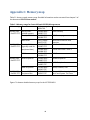
Appendix C: Memory map
Table C.1 shows a rough memory map. Detailed information can be extracted from chapter 2 of
the document LPC17xx User manual.
Table C.1 Memory usage for Coretx-M3 and LPC1768 Microprocessor
Address range General use
Address range for Description
MCB1700
0x0000 0000
On-chip non0x0000 0000 –
Flash memory
– 0x1FFF FFFF volatile memory
0x0007 FFFF
On-chip SRAM
0x1000 0000 –
32 kB user program memory
0x1000 7FFF
Boot ROM
0x1FFF 0000 –
8 kB boot ROM with flash
0x1FFF 1FFF
services
0x2000 0000
On-chip SRAM
0x2007 C000 –
16 kB AHB SRAM – Bank 0
– 0x3FFF FFFF (typically used for
0x2007 FFFF
peripheral data)
0x2008 0000 –
16 kB AHB SRAM – Bank 1
0x2008 3FFF
GPIO
0x2009 C000 –
16 kB
0x2009 FFFF
0x4000 0000
APB Peripherals
0x4000 0000 –
APB0 Peripherals
– 0x5FFF FFFF
0x4007 FFFF
0x4008 0000 –
APB1 Peripherals
0x400F FFFF
AHB Peripherals
0x5000 0000 –
DMA, Ethernet, USB
0x501F FFFF
0xE000 0000
Cortex-M3 Private
0xE000 0000 –
Cortex-M3 functions including
– 0xE00F FFFF Peripheral Bus
0xE00F FFFF
NVIC and System Tick Timer
Figure C.1 shows a detailed memory map for the LPC1768 MCU.
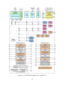
40
Figure C.1 – Detailed memory map for LPC1768 microprocessor
41
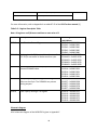
Appendix D: Input / Output ports
Detailed information on this topic can be found in chapters 7, 8, and 9 of the document LPC17xx
User manual [1].
The LPC1768 microprocessor on the MCB1700 board has 100 pins, as shown in figure D.1. Figure
D.2 shows the functionality of selected pins which we are interested in.
Figure D.1 – The LPC1768 microprocessor in LQFP100 pin configuration [1]
As you can see in figure 2, many pins can have more than one function. For example, pin number
73, named as P2.2, can take four different roles as indicated by P2.2/PWM1.3/CTS1/TRACEDATA3.
Actually many pins of LPC1768 can have up to four different functionalities. For each pin there is a
two bit field in a register named PINSELx that determines the functionality of the pin. Table D.1
shows how two the bits choose pin functionality. For more information refer to Appendix A or
tables 79 to 86 of the LPC17xx User manual.
We define the pins we are going to work with as GPIO (general purpose input output) – the
default functionality!
42
Figure D.2 – LED connections to NXP LPC1768 [4]
There are ten PINSEL (pin select) registers. Two of them, PINSEL3 and PINSEL4, are used for pins
connected to LEDs. The PINSEL3 (address 0x4002 C00C) controls P1[31:16] pins and the PINSEL4
(0x4002 C010) controls P2[15:0] pins. Table D.2 shows pin function select for PINSEL3 (partial), and
table D.3 shows pin function select for PINSEL4 (partial). Pins connected to LEDs have bold purple
font. You should also find the pins connected to INT0 and Joystick centre push buttons.
43
Table D.1 – Pin function select register bits
PINSEL0..9 values
Function
Value after reset
00
Primary (default) function, typically GPIO port
01
First alternate function
10
Second alternate function
11
Third alternate function
00
Table D.2- Pin function select register 3
PINSEL3
Pin
name
Function when 00
Function
when 01
Function
when 10
Function
when 11
19:18
P1.25
GPIO Port 1.25
MCOA1
Reserved
MAT1.1
21:20
P1.26
GPIO Port 1.26
MCOB1
PWM1.6
CAP0.0
23:22
P1.27
GPIO Port 1.27
CLKOUT
USB_OVRCR
CAP0.1
25:24
P1.28
GPIO Port 1.28
MCOA2
PCAP1.0
MAT0.0
27:26
P1.29
GPIO Port 1.29
MCOB2
PCAP1.1
MAT0.1
29:28
P1.30
GPIO Port 1.30
Reserved
VBUS
AD0.4
31:30
P1.31
GPIO Port 1.31
Reserved
SCK1
AD0.5
Reset
value
LED
LED[7]
00
LED[6]
LED[5]
Table D.3- Pin function select register 4
PINSEL4
Pin
name
Function when 00
Function
when 01
Function
when 10
Function
when 11
1:0
P2.0
GPIO Port 2.0
PWM1.1
TXD1
Reserved
3:2
P2.1
GPIO Port 2.1
PWM1.2
RXD1
Reserved
44
Reset
value
LED
5:4
P2.2
GPIO Port 2.2
PWM1.3
CTS1
Reserved
LED[4]
7:6
P2.3
GPIO Port 2.3
PWM1.4
DCD1
Reserved
LED[3]
9:8
P2.4
GPIO Port 2.4
PWM1.5
DSR1
Reserved
11:10
P2.5
GPIO Port 2.5
PWM1.6
DTR1
Reserved
LED[1]
13:12
P2.6
GPIO Port 2.6
PCAP1.6
RI1
Reserved
LED[0]
15:14
P2.7
GPIO Port 2.7
RD2
RTS1
Reserved
17:16
P2.8
GPIO Port 2.8
TD2
TXD2
ENET_MDC
00
LED[2]
Each GPIO pin can be either input or output. It can also have a pull-up resistor, pull-down resistor,
or no resistor at all. Figure D.3 shows general structure for a GPIO pin.
Figure D.3 – General structure of a GPIO pin
For output configuration, the pull-up resistor can generate a high (or 1) state, and the opencollector transistor can generate a low (or 0) state when the transistor is turned on.
For input configuration, the open-collector transistor is off.
There is a two bit field in the register named PINMODEx that determines the GPIO pin
configuration. Table D.4 shows how it is done.
Table D.4 – Pin mode configuration (pull-up/pull-down resistor configuration)
PINMOD0 to PINMODE9 values
Function
00
pin has a pull-up resistor enabled
01
pin has repeater mode enabled
Value after reset
00
45
10
pin has neither pull-up nor pull-down
11
Pin has a pull-down resistor enabled
For more information, refer to Appendix A or tables 87-93 of the LPC17xx User manual [1].
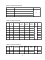
Table D.5 – Register Description Table
Note: All registers are R/W access and have a reset value of 0.
Name
FIODIR
FIOMASK
FIOPIN
FIOSET
FIOCLR
Description
PORTn Register Name
and Address
Port Direction Control Reg.
FIO0DIR – 0x2009 C000
FIO1DIR – 0x2009 C020
FIO2DIR – 0x2009 C040
FIO3DIR – 0x2009 C060
FIO4DIR – 0x2009 C080
Mask register for R/W, set and clears (not used in
FIO0MASK – 0x2009 C010
ECE 222) A one masks or blocks access to a pin.
FIO1MASK – 0x2009 C030
FIO2MASK – 0x2009 C050
FIO3MASK – 0x2009 C070
FIO4MASK – 0x2009 C090
Read IO Pin value and mask (AND) it with the
FIO0PIN – 0x2009 C014
inverted FIOMASK value
FIO1PIN – 0x2009 C034
FIO2PIN – 0x2009 C054
FIO3PIN – 0x2009 C074
FIO4PIN – 0x2009 C094
Set a pin by writing a 1 to register. Writing 0 has no FIO0SET – 0x2009 C018
effect on the IO pin. The FIOMASK can prevent
FIO1SET – 0x2009 C038
setting outputs.
FIO2SET – 0x2009 C058
FIO3SET – 0x2009 C078
FIO4SET – 0x2009 C098
Clear a pin by writing a 1 to register
FIO0CLR – 0x2009 C01C
FIO1CLR – 0x2009 C03C
FIO2CLR – 0x2009 C05C
FIO3CLR – 0x2009 C07C
FIO4CLR – 0x2009 C09C
Schematic diagram
A full schematic diagram of the MCB1700 is given in Appendix F.
46
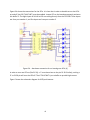
Figure D.4 shows the connections for the LEDs. It is clear that in order to be able to turn the LEDs
on and off, the IC9 (74LVC244T) must be enabled. Jumper LED on the board permanently activates
this buffer IC. The eight inputs of A1~A8 to IC9 are coming directly from the LPC1768. Three inputs
are from port number 1, and five inputs are from port number 2.
Figure D.4 – Hardware connection for on-board green LEDs [4]
In order to turn one LED on (like P1.28), a ‘1’ must be written to the pin P1.28. Similarly, writing a
‘0’ to P1.28 pin will turn the LED off. The IC 74LVC244T is just a buffer to provide high current.
Figure 5 shows the schematic diagram for INT0 push buttons.
47
Figure D.5 – Schematic diagram for the INT0 push button [4]
Appendix E: Exception and Interrupts
The LPC1768 microprocessor can have many sources of interrupts. Selected GPIO pins can also be
set to generate interrupts.
The Nested Vectored Interrupt Controller (NVIC) is an integral part of the ARM Cortex-M3. In the
LPC17xx microprocessors the NVIC supports 35 vectored interrupts. The default location for the
vectors is address 0x0.
The push button INT0 is connected to pin P2.10 of the LPC1768 microprocessor. This pin can be a
source of external interrupts to the MCU. Table E.1 shows different functionalities that can be
assigned to P2.10 pin.
For our purpose there is no big difference between the three types of interrupt sources. For
simplicity you may choose to go ahead with the default state which is GPIO.
Table E.1 – Pin functions for P2.10
Bits 21:20 of PINSEL4
Function
00
GPIO P2.10 pin (default)
̅̅̅̅̅̅̅̅̅
01
10
NMI
11
Reserved
48
Value after reset
00
If you choose to consider the P2.10 as GPIO, then you should also enable this source of interrupt
as described in section 9.5.6 of the document LPC17xx User manual [1]. You can set the P2.10 pin
to be sensitive to either the rising edge or the falling edge.
More information on clearing the interrupt pending pin can be found in table 123 in section
9.5.6.11 – page 139 of [1].
49
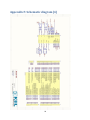
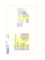
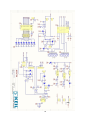
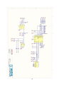
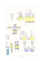
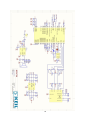
Appendix F: Schematic diagram [4]
50
51
52
53
54
55
References:
[1] LPC17xx User manual, Literature number UM10360, Rev.2, August 19, 2010, Published by
NXP®. Can be accessed online: http://www.nxp.com/documents/user_manual/UM10360.pdf
(Accessed on June 18, 2012)
[2] Getting Started, Creating Applications with μVision®4, Published by Keil®. Can be accessed
online: http://www.keil.com/product/brochures/uv4.pdf (Accessed on June 18, 2012)
[3] ECE-455 Lab manual, Bernie Roehl, E&CE Department, University of Waterloo. Can be accessed
online: https://ece.uwaterloo.ca/~ece455/lab_manual.pdf (Accessed on June 18, 2012)
[4] Schematic Diagram for the MCB1700 board, Published by Keil®. Can be accessed online:
http://www.keil.com/mcb1700/mcb1700-schematics.pdf (Accessed on June 18, 2012)
[5] Snap-shots taken from the Keil µVision4 software.
[6] “Morse Code”, From Wikipedia, the free encyclopedia. Can be accessed online:
http://en.wikipedia.org/wiki/Morse_code (Accessed on August 21, 2012)
[7] Cortex™-M3 Devices, Generic User Guide, Published by ARM. Can be accessed online:
http://infocenter.arm.com/help/topic/com.arm.doc.dui0552a/DUI0552A_cortex_m3_dgug.pdf
(Accessed on August 21, 2012)
56