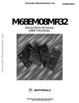
1
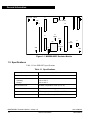
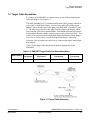
User’s Manual EML08EYUM/D Version 1.0 May 2, 2002 M68EML08EY Emulation Module User’s Manual © Motorola, Inc., 2002 Important Notice to Users While every effort has been made to ensure the accuracy of all information in this document, Motorola assumes no liability to any party for any loss or damage caused by errors or omissions or by statements of any kind in this document, its updates, supplements, or special editions, whether such errors are omissions or statements resulting from negligence, accident, or any other cause. Motorola further assumes no liability arising out of the application or use of any information, product, or system described herein: nor any liability for incidental or consequential damages arising from the use of this document. Motorola disclaims all warranties regarding the information contained herein, whether expressed, implied, or statutory, including implied warranties of merchantability or fitness for a particular purpose. Motorola makes no representation that the interconnection of products in the manner described herein will not infringe on existing or future patent rights, nor do the descriptions contained herein imply the granting or license to make, use or sell equipment constructed in accordance with this description. Trademarks This document includes these trademarks: Motorola and the Motorola logo are registered trademarks of Motorola, Inc. Windows is a registered trademark of Microsoft Corporation in the U.S. and other countries. Intel is a registered trademark of Intel Corporation. Motorola, Inc., is an Equal Opportunity / Affirmative Action Employer. For an electronic copy of this book, visit Motorola’s web site at http://e-www.motorola.com/ © Motorola, Inc., 2002; All Rights Reserved M68EML08EY Emulation Module - Version 1.0 2 User’s Manual MOTOROLA User’s Manual — M68EML08EY Emulation Module Table of Contents M68EML08EY Quick Start Guide 1 - Set jumpers W4 and W2 . . . . . . . . . . . . . . . . . . . . . . . . . . . . . . . . . 7 2 - Install the emulation module into your development system . . . . . 7 3 - Connect the emulation module to your target system . . . . . . . . . . . 8 4 - Install the development software. . . . . . . . . . . . . . . . . . . . . . . . . . . 8 5 - Copy personality files to your computer . . . . . . . . . . . . . . . . . . . . . 8 6 - Connect MMDS or MMEVS to your computer and apply power . 9 Section 1. General Information 1.1 Introduction. . . . . . . . . . . . . . . . . . . . . . . . . . . . . . . . . . . . . . . . . . . . . 11 1.2 1.2.1 1.2.2 Development Systems. . . . . . . . . . . . . . . . . . . . . . . . . . . . . . . . . . . . . 11 Motorola Modular Development System (MMDS0508). . . . . . . . 11 Motorola Modular Evaluation System (MMEVS0508). . . . . . . . . 12 1.3 System Requirements . . . . . . . . . . . . . . . . . . . . . . . . . . . . . . . . . . . . . 13 1.4 EM Layout . . . . . . . . . . . . . . . . . . . . . . . . . . . . . . . . . . . . . . . . . . . . . 13 1.5 Specifications . . . . . . . . . . . . . . . . . . . . . . . . . . . . . . . . . . . . . . . . . . . 14 1.6 Target Cable Assemblies . . . . . . . . . . . . . . . . . . . . . . . . . . . . . . . . . . 15 Section 2. Preparation and Operation 2.1 Introduction. . . . . . . . . . . . . . . . . . . . . . . . . . . . . . . . . . . . . . . . . . . . . 17 2.2 Configuring Board Components . . . . . . . . . . . . . . . . . . . . . . . . . . . . . 17 2.3 Limitations . . . . . . . . . . . . . . . . . . . . . . . . . . . . . . . . . . . . . . . . . . . . . 19 2.4 Remaining System Installation . . . . . . . . . . . . . . . . . . . . . . . . . . . . . . 19 User’s Manual MOTOROLA M68EML08EY Emulation Module - Version 1.0 Table of Contents 1 Table of Contents Section 3. Support Information 3.1 Introduction. . . . . . . . . . . . . . . . . . . . . . . . . . . . . . . . . . . . . . . . . . . . . 21 3.2 Target Connectors J2 and J3 . . . . . . . . . . . . . . . . . . . . . . . . . . . . . . . . 21 3.3 Logic Analyzer Connectors J1 and J5 . . . . . . . . . . . . . . . . . . . . . . . . 24 3.4 Inverted Clock Connector J4 . . . . . . . . . . . . . . . . . . . . . . . . . . . . . . . 25 3.5 Analog-to-Digital Converter Reference Voltage Connector E2. . . . . 26 3.6 Board Factory Test Connector J6 . . . . . . . . . . . . . . . . . . . . . . . . . . . . 26 3.7 Optional crystal circuit using Y1 . . . . . . . . . . . . . . . . . . . . . . . . . . . . 26 3.8 Clock oscillator Y2 . . . . . . . . . . . . . . . . . . . . . . . . . . . . . . . . . . . . . . . 27 3.9 EM Board Socket Connectors P1 and P2 . . . . . . . . . . . . . . . . . . . . . . 27 M68EML08EY Emulation Module - Version 1.0 2 User’s Manual Table of Contents MOTOROLA User’s Manual — M68EML08EY Emulation Module List of Figures 1-1 1-2 3-1 3-2 3-3 3-4 3-5 3-6 3-7 3-8 M68EML08EY Emulator Module. . . . . . . . . . . . . . . . . . . . . . . . . . . 14 Target Cable Assembly . . . . . . . . . . . . . . . . . . . . . . . . . . . . . . . . . . . 15 Target Connector (J2) Pin Assignments . . . . . . . . . . . . . . . . . . . . . . 21 Target Connector (J3) Pin Assignments . . . . . . . . . . . . . . . . . . . . . . 23 Logic Analyzer Connector J1 Pin Assignments . . . . . . . . . . . . . . . . 24 Logic Analyzer Connector J5 Pin Assignments . . . . . . . . . . . . . . . . 25 Connector J4 Pin Assignments . . . . . . . . . . . . . . . . . . . . . . . . . . . . . 25 Connector E2 Pin Assignments . . . . . . . . . . . . . . . . . . . . . . . . . . . . . 26 EM Connector P1 Pin Assignments. . . . . . . . . . . . . . . . . . . . . . . . . . 28 EM Connector P2 Pin Assignments. . . . . . . . . . . . . . . . . . . . . . . . . . 30 User’s Manual MOTOROLA M68EML08EY Emulation Module - Version 1.0 List of Figures 3 List of Figures M68EML08EY Emulation Module - Version 1.0 4 User’s Manual List of Figures MOTOROLA User’s Manual — M68EML08EY Emulation Module List of Tables 1-1 1-2 2-1 3-1 3-2 3-3 3-4 3-5 3-6 3-7 3-8 Specifications. . . . . . . . . . . . . . . . . . . . . . . . . . . . . . . . . . . . . . . . . . . 14 EML08EY Target Cable and Head Assemblies . . . . . . . . . . . . . . . . 15 Configuration Components . . . . . . . . . . . . . . . . . . . . . . . . . . . . . . . . 17 Target Connector (J2) Signal Descriptions . . . . . . . . . . . . . . . . . . . . 22 Target Connector (J3) Signal Descriptions . . . . . . . . . . . . . . . . . . . . 23 Logic Analyzer Connector J1 Signal Descriptions . . . . . . . . . . . . . . 24 Logic Analyzer Connector J5 Signal Descriptions . . . . . . . . . . . . . . 25 Connector J4 Signal Descriptions . . . . . . . . . . . . . . . . . . . . . . . . . . . 25 Connector E2 Signal Descriptions . . . . . . . . . . . . . . . . . . . . . . . . . . . 26 EM Connector P1 Signal Descriptions . . . . . . . . . . . . . . . . . . . . . . . 29 EM Connector P2 Signal Descriptions . . . . . . . . . . . . . . . . . . . . . . . 31 User’s Manual MOTOROLA M68EML08EY Emulation Module - Version 1.0 List of Tables 5 List of Tables M68EML08EY Emulation Module - Version 1.0 6 User’s Manual List of Tables MOTOROLA User’s Manual — M68EML08EY Emulation Module M68EML08EY Quick Start Guide Make sure that power is disconnected from your M68EML08EY Emulator Module and from your target system. Then follow these quick-start steps to make your M68EML08EY ready for use as quickly as possible. 1 - Set jumpers W4 and W2 Jumper header W4 specifies the clock source for the MCU when you enable its external clock. • Place the jumper between pins 3 and 4 (factory default) to specify the debugger-controlled oscillator from the platform board or place the jumper between pins 1 and 2 to specify 4.9152-MHz oscillator Y2, which can be replaced with an oscillator of a different value. Jumper header W2 specifies the voltage supplied to the emulation module MCU and to signals driven to the target. • Place the jumper between pins 1 and 2 (factory default) to specify fixed 5.0 volts DC or place the jumper between pins 3 and 4 to specify fixed 3.0 volts DC. 2 - Install the emulation module into your development system To use the M68EML08EY in an MMDS0508 Motorola Modular Development System (MMDS) or MMEVS0508 Motorola Modular Evaluation System (MMEVS): User’s Manual MOTOROLA • Remove the access panel of the MMDS station-module enclosure. • Insert the M68EML08EY through the access-panel opening. M68EML08EY Emulation Module - Version 1.0 M68EML08EY Quick Start Guide 7 M68EML08EY Quick Start Guide • Fit together M68EML08EY connectors P1 and P2 (on the bottom of the board) to connectors P11 and P12, respectively, of the MMDS or MMEVS (P6 and P7 on some MMEVS boards) control board and snap the corners of the M68EML08EY onto the plastic standoffs. 3 - Connect the emulation module to your target system Use the supplied target flex cable, appropriate target head adapter, and surface mount adapter. Plug the appropriate end of the flex cable plugs into M68EML08EY connectors J2 and J3. • If the M68EML08EY is in an MMDS station module, run the flex cable through the slit in the station-module enclosure, then replace the access panel. • Plug the other end of the flex cable into the target head. Solder the appropriate surface mount adapter to your target if necessary. Then plug the target head into the surface mount adapter on your target system. 4 - Install the development software 5 - Copy personality files to your computer The factory ships M68EML08EY MCU personality files on the documentation CD-ROM. • If you’re using the CodeWarrior IDE, find the installation directory and copy the personality files named 00C31Vxx.mem and 00C32Vxx.mem from the documentation CD-ROM to the ...\prog\reg subdirectory of the CodeWarrior IDE main directory. • If you’re using the P&E debugger, copy these files to the installation directory that contains MMDS08.EXE or MMEVS08.EXE and rename them from 00C31Vxx.mem and 00C32Vxx.mem to 00431Vxx.mem and 00432Vxx.mem respectively. M68EML08EY Emulation Module - Version 1.0 8 M68EML08EY Quick Start Guide User’s Manual MOTOROLA M68EML08EY Quick Start Guide 6 - Connect MMDS or MMEVS to your computer and apply power 6 - Connect MMDS or MMEVS to your computer and apply power This completes the quick start for your M68EML08EY. When you make sure that cable connections between your development system and your computer are sound, you are ready to apply power and use your M68EML08EY. User’s Manual MOTOROLA M68EML08EY Emulation Module - Version 1.0 M68EML08EY Quick Start Guide 9 M68EML08EY Quick Start Guide M68EML08EY Emulation Module - Version 1.0 10 M68EML08EY Quick Start Guide User’s Manual MOTOROLA User’s Manual — M68EML08EY Emulation Module Section 1. General Information 1.1 Introduction This user’s manual explains connection and configuration of the Motorola M68EML08EY Emulator Module (EML08EY). The EML08EY makes possible emulation and debugging of target systems based on an MC68HC908EY16 or MC68HC908EY8 microcontroller unit (MCU). The EML08EY can be part of two development systems. This section describes those systems and explains the layout of the EML08EY. 1.2 Development Systems Your EML08EY can be part of two Motorola HC08 processor family development systems: the MMDS0508 Motorola Modular Development System (MMDS) or the MMEVS0508 Evaluation System (MMEVS). Refer to the specific development system user’s manual for more information. 1.2.1 Motorola Modular Development System (MMDS0508) The MMDS is an emulator system that provides a bus state analyzer and real-time memory windows for designing and debugging a target system. A complete MMDS consists of: • a station module — the metal MMDS enclosure, containing the platform board and the internal power supply. Most system cables connect to the MMDS station module. • an emulator module (EM) — such as the EML08EY, a separatelypurchased printed circuit board that enables system functionality for a specific set of MCUs. The EM fits into the station module through a removable panel in the enclosure top. The EM has connectors for a target cable and for cables to a logic analyzer. The cable runs to an optional target system through an aperture in the station-module enclosure, to connect directly to the emulator module. User’s Manual MOTOROLA M68EML08EY Emulation Module - Version 1.0 General Information 11 General Information • two logic clip cable assemblies — twisted-pair cables that connect the station module to your target system, a test fixture, an oscillator, or any other circuitry useful for evaluation or analysis. One end of each cable assembly has a molded connector, which fits into station-module pod A or pod B. Leads at the other end of each cable terminate in female probe tips. Ball clips come with the cable assemblies and may be attached to the female probe tips. • a 9-lead RS-232 serial cable — the cable that connects the MMDS to the host computer RS-232 port. • system software — development software, on CD-ROM. • MMDS0508 documentation — an MMDS operations manual (MMDS0508OM/D) and the appropriate EM user’s manual. You select the MMDS baud rate: 1200, 2400, 4800, 9600, 19200, 38400, or 57600. Substituting a different EM enables your MMDS to emulate target systems based on different MCUs or MCU families. (Your Motorola representative can explain all the EMs available.) 1.2.2 Motorola Modular Evaluation System (MMEVS0508) An MMEVS is an economical tool for designing, debugging, and evaluating target systems. A complete MMEVS consists of: • a platform board (PFB) — the bottom board, which supports the emulator module. The platform board has connectors for power and the the terminal or host computer. • an emulator module (EM) — such as the EML08EY, a separately purchased printed circuit board that enables system functionality for a specific set of MCUs. The EM fits onto the PFB. The EM has connectors for the target cable and for cables to a logic analyzer. • a 9-to-25-pin adapter — a molded assembly that lets you connect the 9-pin cable to a 25-pin serial port. • a 9-lead RS-232 serial cable — the cable that connects the station module to the host computer RS-232 port. • system software — development software, on CD-ROM. M68EML08EY Emulation Module - Version 1.0 12 User’s Manual General Information MOTOROLA General Information System Requirements • MMEVS0508 documentation — an MMEVS operations manual (MMEVSOM/D) and the appropriate EM user’s manual. An MMEVS features automatic baud rate selection: 2400, 4800, 9600, 19200, 38400, or 57600. Substituting a different EM enables your MMEVS to emulate target systems based on different MCUs or MCU families. (Your Motorola representative can explain all the EMs available.). 1.3 System Requirements An IBM PC or compatible running Windows 98, Windows 2000, or Windows NT (version 4.0) with at least 32MB of RAM and an RS-232 serial port. 1.4 EM Layout Figure 1-1 shows the layout of the EML08EY. Jumper header W2 specifies the operating voltage. Jumper header W4 specifies the clock signal source. Jumper header W1 controls unification of analog ground references. Jumper header W3 specifies the MCU to be emulated. Target interface connectors J2 and J3 connect the EML08EY to a target system, via the included target cable assembly. If you use your EML08EY as part of an MMDS, run the target cable assembly through the slit in the station module enclosure. Connectors J1 and J5 connect to a logic analyzer. Connector J4 is the source for an inverted clock signal. DIN connectors P1 and P2, on the bottom of the board connect the EML08EY to the platform board. The emulation MCU is at location U2. Connector J6 is for EM board design and factory use only. User’s Manual MOTOROLA M68EML08EY Emulation Module - Version 1.0 General Information 13 General Information E1 W2 VMCU Sel VMCU GND U2 J1 W1 E2 VSSA A/D REF GND P2 P1 J2 J3 J4 OSC2 J5 U21 U23 GND W4 OSC Sel Y2 W3 MCU Sel J6 GND Figure 1-1 M68EML08EY Emulator Module 1.5 Specifications Table 1-1 lists EML08EY specifications Table 1-1 Specifications Characteristic Specifications Maximum Clock speed 32-MHz at 5V, 16-MHz at 3V Temperature operating storage -10° to +50° C -40° to +85° C MCU Extension I/O HCMOS Compatible at Vmcu (5V or 3V) Relative humidity 0 to 90% (noncondensing) Power requirements 5VDC supplied from the MMDS or MMEVS Dimensions 5.5 X 8.0 X 0.75 inches (139.7 x 203.2 x 19.1 mm) M68EML08EY Emulation Module - Version 1.0 14 User’s Manual General Information MOTOROLA General Information Target Cable Assemblies 1.6 Target Cable Assemblies To connect your EML08EY to a target system, you need the included target cable and adapters. See Figure 1-2. The cable assembly for a 32-pin thin quad flat pack (QFP) package consists of: a flex cable, a target head adapter, a socket-saver and a QFP surface mount adapter. One end of the target cable plugs onto EML08EY connectors J2 and J3. The other end of the flex cable plugs onto the target head adapter, which plugs onto the QFP surface mount adapter. You should solder the QFP surface mount adapter directly onto the target-system board in place of the MCU. The socket-saver goes between the target head adapter and surface mount adapter. If you use it, it will reduce wear on the target head adapter. After many insertions, you can replace the socket-saver without replacing the entire target head adapter. Table 1-2 lists target cable and head part numbers appropriate for the EML08EY. Table 1-2 EML08EY Target Cable and Head Assemblies MCU Package Flex Cable Part Number Target Head Adapter Part Number Surface Mount Adapter Part Number 32-pin QFP-FA M68CBL05C M68TC08EYFA32 M68TQP032SA1 Socket-Saver Part Number M68TQS032SAG1 Figure 1-2 Target Cable Assembly User’s Manual MOTOROLA M68EML08EY Emulation Module - Version 1.0 General Information 15 General Information M68EML08EY Emulation Module - Version 1.0 16 User’s Manual General Information MOTOROLA User’s Manual — M68EML08EY Emulation Module Section 2. Preparation and Operation 2.1 Introduction This section explains EML08EY preparation: how to set board jumpers and how to make system connections. Note that you can reconfigure an EML08EY already installed in an MMDS0508 station module enclosure. To do so, switch off station-module power and target power, remove the panel, then follow the guidance of this section. Similarly, you can reconfigure an EML08EY already installed on the MMEVS platform board, provided that you disconnect platform-board power and target power. CAUTION: ESD Protection Motorola development systems include open-construction printed circuit boards that contain static-sensitive components. These boards are subject to damage from electrostatic discharge (ESD). To prevent such damage, you must use static-safe work surfaces and grounding straps, as defined in ANSI/EOS/ESD S6.1 and ANSI/EOS/ESD S4.1. All handling of these boards must be in accordance with ANSI/EAI 625. 2.2 Configuring Board Components Table 2-1 is a summary of configuration settings. Table 2-1 Configuration Components Component Position Voltage Select Header, W2 (Use only one jumper in this header.) Effect 5V: Specifies 5.0-volt operating power. W2 1 2 5 6 Factory setting 3V: Specifies 3.0-volt operating power. W2 User’s Manual MOTOROLA 1 2 5 6 M68EML08EY Emulation Module - Version 1.0 Preparation and Operation 17 Preparation and Operation Table 2-1 Configuration Components (Continued) Component Position Effect ADJ: Specifies the adjustable voltage that variable resistor VR1 (if installed) controls (2.7V to 5.5V). W2 1 2 5 6 Oscillator Select Header, W4 (Use only one jumper in this header.) PFB: Specifies the oscillator clock signal from the platform board (PFB). W4 1 2 5 6 Factory setting EM: Specifies the clock signal from the 4.915-megahertz oscillator on the EM board at Y2 (EM). W4 1 2 5 6 XTAL: Specifies the clock signal from a user-supplied crystal installed at Y1 (XTAL). W4 Analog Ground (VSSA) Unify Header, W1 1 2 5 6 DIS: Separates analog ground references of the processor and the board. W1 3 Factory setting 1 EN: Unifies analog ground references of the processor and the target board: VSSA = VREF_LOW = AGND. (This configuration increases sensitivity to noise.) W1 3 1 MCU Emulation Select Header, W3 EY16: Specifies emulation of an EY16 processor. W3 Factory setting 3 1 EY8: Specifies emulation of an EY8 processor. W3 3 1 M68EML08EY Emulation Module - Version 1.0 18 Preparation and Operation User’s Manual MOTOROLA Preparation and Operation Limitations Table 2-1 Configuration Components (Continued) Component Position Voltage Adjust Resistor, VR1 VR1 Effect Specifies board operating power, from 2.7 through 5.5 volts, provided that the W2 jumper is between pins 5 and 6. Turn the screw to adjust the voltage. This component may not be installed on some boards. 2.3 Limitations Limitations listed here apply to using your EML08EY versus using the actual MCU in your target system: Limitation 1 - Crystals: You can install a crystal at location Y1 and associated components (refer to the schematic) to be a clock signal source. But each crystal has slightly different characteristics, and a crystal’s behavior can differ substantially in different circuits. Satisfactory performance as part of the EML08EY Y1 timing circuit does not guarantee that the same crystal will perform satisfactorily on a target board. Limitation 2 - OSC2: When PTC3 is set in register CONFIG2 to provide OSC2, it will not be available on the target cable. If you wish to use this signal on your target, you must make a connection between J4 and your target system. Limitation 3 - STOP Mode: The emulator may not be able to recover from STOP mode entry if it is running from the external clock source on the EM board (EM, PFB, or XTAL). 2.4 Remaining System Installation When you have configured jumper headers, you are ready to complete EML08EY installation: User’s Manual MOTOROLA • To install the EML08EY in an MMDS0508 station module, remove the panel from the station module top. Fit together EM connectors P1 and P2 (on the bottom of the board) and platform-board connectors P11 and P12, respectively. Snap the corners of the EM onto the plastic standoffs. Connect the target cable, if appropriate, then replace the panel. • If your EML08EY already is installed in the station module, reconnect the target cable (if necessary). Replace the panel. M68EML08EY Emulation Module - Version 1.0 Preparation and Operation 19 Preparation and Operation • To install the EML08EY on an MMEVS platform board, fit together EM connectors P1 and P2 (on the bottom of the board) and platform-board connectors P11 and P12 (P6 and P7 on some MMEVS boards), respectively. Snap the corners of the EM onto the plastic standoffs. • If you will use the P&E development system, copy personality files 00C31Vxx.MEM and 00C32Vxx.MEM from the documentation CD-ROM to the installation directory that contains file MMDS08.EXE or MMEVS08.EXE. Then rename these files to 00431Vxx.MEM and 00432Vxx.MEM. • If you will use the CodeWarrior IDE development software, copy personality files 00C31Vxx.MEM and 00C32Vxx.MEM from the documentation CD-ROM to the ...\prog\mem subdirectory of the CodeWarrior IDE installation directory. Additionally, if you must use CodeWarrior IDE development software, you will need to copy the EML08EY register files MCU0C31.REG and MCU0C32.REG from the documentation CD-ROM to the ...\prog\reg subdirectory of the CodeWarrior IDE installation directory. The CodeWarrior IDE uses these files to implement optional functionality such as letting you view or modify register contents by name rather than by address. A register file is an ASCII text file, which you may customize. (The CodeWarrior IDE user’s manual explains how to create and use such files.) At this point, you are ready to make any remaining cable connections and apply power. For instructions, consult the MMDS or MMEVS operations manual. M68EML08EY Emulation Module - Version 1.0 20 Preparation and Operation User’s Manual MOTOROLA User’s Manual — M68EML08EY Emulation Module Section 3. Support Information 3.1 Introduction This section consists of connector pin assignments, connector signal descriptions, and other information that may be useful in your development activities. 3.2 Target Connectors J2 and J3 Connectors J2 and J3 are the EML08EY target connectors. Figure 3-1 and Table 3-1 give the pin assignments and signal descriptions for connector J2. Figure 3-2 and Table 3-2 give the pin assignments and signal descriptions for connector J3. G G G G PB3 PB4 PB5 PB6 PB7 G G G PC4 PA0 PA4 G PE0 PA6 IRQ PD0 1 3 5 7 9 11 13 15 17 19 21 23 25 27 29 31 33 35 37 39 J2 • • • • • • • • • • • • • • • • • • • • • • • • • • • • • • • • • • • • • • • • 2 4 6 8 10 12 14 16 18 20 22 24 26 28 30 32 34 36 38 40 G G G G G G G G G G RST G PC3 G PA3 EV PE1 PA5 G G Figure 3-1 Target Connector (J2) Pin Assignments User’s Manual MOTOROLA M68EML08EY Emulation Module - Version 1.0 Support Information 21 Support Information Table 3-1 Target Connector (J2) Signal Descriptions Pin Label Signal 1 — 8, 10, 12, 14, 16, 18 — 21, 23, 24, 28, 31, 38, 40 G 9, 11, 13, 15, 17 PB3 — PB7 22 RST 25, 26 PC4, PC3 PORT C (lines 4, 3) — General-purpose I/O lines controlled by software via data direction and data registers. (Other port C lines are available on connector J4.) 27, 29, 30, 35, 36 PA0, PA3 — PA6 (not in exact order) PORT A (lines 0, 3—6) — General-purpose I/O lines controlled by software via data direction and data registers. (Port A lines 1 and 2 are available on connector J4.) 32 EV 33, 34 PE0, PE1 37 IRQ TARGET INTERRUPT — Active-low input line for requesting a target interrupt. 39 PD0 PORT D (line 0) — General-purpose I/O lines controlled by software via data direction and data registers. (Port D line 1 is available on connector J4.) GROUND PORT B (lines 3—7) — General-purpose I/O lines controlled by software via data direction and data registers. (Other port B lines are available on connector J4.) RESET — Active-low signal. If an output, starts a target reset. If an input, confirms reset of the target MCU. EXTERNAL VOLTAGE DETECT — Input signal that detects target-system power-up. PORT E (lines 0, 1) — General-purpose I/O lines controlled by software via data direction and data registers. M68EML08EY Emulation Module - Version 1.0 22 User’s Manual Support Information MOTOROLA Support Information Target Connectors J2 and J3 VSSA PB0 PB1 PB2 G G G G G G G G PC2 G PA2 G G PC1 G PD1 1 3 5 7 9 11 13 15 17 19 21 23 25 27 29 31 33 35 37 39 J3 • • • • • • • • • • • • • • • • • • • • • • • • • • • • • • • • • • • • • • • • 2 4 6 8 10 12 14 16 18 20 22 24 26 28 30 32 34 36 38 40 VSSA G G G G G G G G G G G G G PA1 G G PC0 G G Figure 3-2 Target Connector (J3) Pin Assignments Table 3-2 Target Connector (J3) Signal Descriptions Pin Label Signal 1, 2 VSSA TARGET ANALOG GROUND — Analog-ground reference signal from the target. 3, 5, 7 PB0 — PB2 4, 6, 8 — 24, 26 — 28, 31 — 34, 37, 38, 40 G 25, 35, 36 PC2 — PC0 PORT C (lines 2—0) — General-purpose I/O lines controlled by software via data direction and data registers. (Port C lines 3 and 4 are available on connector J3.) 29, 30 PA2, PA1 PORT A (lines 2, 1) — General-purpose I/O lines controlled by software via data direction and data registers. (Other port A lines are available on connector J3.) 39 PD1 PORT D (line 1) —General-purpose I/O lines controlled by software via data direction and data registers. (Port D line 0 is available on connector J3.) PORT B (lines 0—2) — General-purpose I/O lines controlled by software via data direction and data registers. (Other port B lines are available on connector J3.) GROUND User’s Manual MOTOROLA M68EML08EY Emulation Module - Version 1.0 Support Information 23 Support Information 3.3 Logic Analyzer Connectors J1 and J5 Connectors J1 and J5 are the EML08EY logic analyzer connectors. Figure 3-3 and Table 3-3 give pin assignments and signal descriptions for connector J1, which has pod 1 signals. Figure 3-4 and Table 3-4 give pin assignments and signal descriptions for connector J5, which has pod 2 signals. NC T12 RST_B TEST TEST LIR_B AD6 AD4 AD2 AD0 1 3 5 7 9 11 13 15 17 19 J1 • • • • • • • • • • • • • • • • • • • • 2 4 6 8 10 12 14 16 18 20 NC LBOX NC EMUX LRW AD7 AD5 AD3 AD1 GND Figure 3-3 Logic Analyzer Connector J1 Pin Assignments Table 3-3 Logic Analyzer Connector J1 Signal Descriptions Pin Label Signal 1, 2, 6 NC No connection 3 T12 SYSTEM BUS CLOCK — Clock that matches the internal emulation MCU bus clock 4 LBOX LAST BUS CYCLE — Output signal that the emulator asserts to indicate that the target system MCU is in the last bus cycle of an instruction. 5 RST_B COP RESET — Active-low output signal indicating (1) the target driving its reset pin, or (2) the platform board driving a reset to the emulator module. 7, 9 TEST Test pins are used only during system development and factory test. 8 EMUX MUXED CONTROL — Output from the emulation MCU that, during different phases of the clock, drives R/W, LIR_B, and LAST signals. 10 LRW LATCHED READ/WRITE — Output signal from the target MCU. If high, the target MCU is reading. If low, the target MCU is writing. 11 LIR_B LOAD INSTRUCTION REGISTER — Active-low output signal indicating that the target MCU is fetching an instruction. 12 — 19 AD7 — AD0 20 GND PFB DATA BUS (lines 7—0) — Outputs the data lines going to the platform board. GROUND M68EML08EY Emulation Module - Version 1.0 24 User’s Manual Support Information MOTOROLA Support Information Inverted Clock Connector J4 NC ECLK A14 A12 A10 A8 A6 A4 A2 A0 1 3 5 7 9 11 13 15 17 19 J5 • • • • • • • • • • • • • • • • • • • • 2 4 6 8 10 12 14 16 18 20 NC A15 A13 A11 A9 A7 A5 A3 A1 GND Figure 3-4 Logic Analyzer Connector J5 Pin Assignments Table 3-4 Logic Analyzer Connector J5 Signal Descriptions Pin Label 1, 2 NC 3 ECLK 4 — 19 A15 — A0 20 GND Signal No connection EM CLOCK — Output clock signal for the emulator module. LATCHED ADDRESS BUS (lines 15—0) — Output showing the address of the current bus cycle. GROUND 3.4 Inverted Clock Connector J4 Connector J4 is the source for an inverted clock signal. Figure 3-5 and Table 3-5 give the pin assignments and signal descriptions for this connector. Because the OSC2 signal is not present on the target cable, you should connect this signal to your target system if you will use the OSC2 signal. J4 • • • 3 2 1 GND OSC2 Figure 3-5 Connector J4 Pin Assignments Table 3-5 Connector J4 Signal Descriptions Pin Label 3 GND Signal Ground User’s Manual MOTOROLA M68EML08EY Emulation Module - Version 1.0 Support Information 25 Support Information Table 3-5 Connector J4 Signal Descriptions (Continued) Pin Label No connection 2 1 Signal OSC2 INVERTED CLOCK OUTPUT — Inversion of the clock signal that jumper header W4 specifies if you select the external clock. Inversion of the ICG clock if you select the internal clock (default). 3.5 Analog-to-Digital Converter Reference Voltage Connector E2 Connector E2 is the source for the filtered A/D reference voltages. Figure 3-6 and Table 3-6 give the pin assignments and signal descriptions for this connector. The factory test uses this connection. E2 • • • 3 2 1 L A/D REF H Figure 3-6 Connector E2 Pin Assignments Table 3-6 Connector E2 Signal Descriptions Pin Label 3 L 2 A/D REF 1 H Signal LOW REFERENCE VOLTAGE No connection (label only) HIGH REFERENCE VOLTAGE 3.6 Board Factory Test Connector J6 Factory tests use this connector. It may not be populated. 3.7 Optional crystal circuit using Y1 When you select the XTAL option on jumper W4 (jumper on pins 5-6), the clock signal generated by Y1 is supplied to the external inputs of the MCU. The circuit that uses crystal Y1 is not populated in production. You can populate this circuit using the default values supplied in the schematic (see page 6). This circuit does not necessarily represent a crystal attached to the MCU. M68EML08EY Emulation Module - Version 1.0 26 User’s Manual Support Information MOTOROLA Support Information Clock oscillator Y2 3.8 Clock oscillator Y2 When you select the EM option on jumper W4 (jumper on pins 1-2), the clock signal generated by Y2 is supplied to the external inputs of the MCU. You can replace Y2 with another compatible clock oscillator to provide a different clock frequency (see schematic page 6). 3.9 EM Board Socket Connectors P1 and P2 Connectors P1 and P2 connect the EML08EY to the platform board. Figure 3-7 and Table 3-7 give pin assignments and signal descriptions for connector P1. Figure 3-8 and Table 3-8 give pin assignments and signal descriptions for connector P2. User’s Manual MOTOROLA M68EML08EY Emulation Module - Version 1.0 Support Information 27 Support Information P1 A • • • • • • • • • • • • • • • • • • • • • • • • • • • • • • • • A1 A2 A3 A4 A5 A6 A7 A8 A9 A10 A11 A12 A13 A14 A15 A16 A17 A18 A19 A20 A21 A22 A23 A24 A25 A26 A27 A28 A29 A30 A31 A32 LA[14] LA[13] LA[12] LA[11] LA[10] LA[9] LA[8] LA[7] LA[6] LA[5] LA[4] LA[3] LA[2] LA[1] LA[0] LA[15] NC NC PFB_IRQ_B CHRGPMP NC NC PFB_OSC NC NC NC NC NC NC NC PFB_VCC GND B • • • • • • • • • • • • • • • • • • • • • • • • • • • • • • • • B1 B2 B3 B4 B5 B6 B7 B8 B9 B10 B11 B12 B13 B14 B15 B16 B17 B18 B19 B20 B21 B22 B23 B24 B25 B26 B27 B28 B29 B30 B31 B32 PFB_AD[7] PFB_AD[6] PFB_AD[5] PFB_AD[4] PFB_AD[3] PFB_AD[2] PFB_AD[1] PFB_AD[0] LIR_B LRW SCLK T12CLK NC NC NC NC INTERNAL_B NC SWITCH_B NC NC NC NC LBOX BREAK_B NC NC NC NC NC PFB_VCC GND C • • • • • • • • • • • • • • • • • • • • • • • • • • • • • • • • C1 C2 C3 C4 C5 C6 C7 C8 C9 C10 C11 C12 C13 C14 C15 C16 C17 C18 C19 C20 C21 C22 C23 C24 C25 C26 C27 C28 C29 C30 C31 C32 GND GND GND GND GND GND GND GND GND GND GND GND GND GND GND GND GND GND GND GND GND GND GND GND GND GND GND GND GND GND GND GND Figure 3-7 EM Connector P1 Pin Assignments M68EML08EY Emulation Module - Version 1.0 28 User’s Manual Support Information MOTOROLA Support Information EM Board Socket Connectors P1 and P2 Table 3-7 EM Connector P1 Signal Descriptions Pin A1 — A16 Mnemonic Signal LA[15] — LA[0] LATCHED ADDRESS BUS (lines 15—0) — Output lines for (not in exact addressing external devices. order) A17, A18, A21, A22, A24 — A30 NC No connection A19 PFB_IRQ_B PFB INTERRUPT — Active-low signal that requests an interrupt of the platform board. A20 CHRGPMP CHARGE PUMP — 12-volt signal (from the platform board). A23 PFB_OSC PFB OSCILLATOR — Oscillator clock signal from the platform board. A31 PFB_VCC PFB POWER — Operating voltage signal from the platform board. A32 GND B1 — B8 PFB_AD[7] — PFB_AD[0] GROUND B9 LIR_B LOAD INSTRUCTION REGISTER — Active-low signal that the target MCU is fetching an instruction. B10 LRW LATCHED READ/WRITE — Input signal from the target MCU. If high, the target MCU is reading. If low, the target MCU is writing. SERIAL CLOCK — Output clock signal to the platform board. PFB ADDRESS (lines 7—0) — Address of the current bus cycle. B11 SCLK B12 T12CLK B13 — B16, B18, B20 — B23, B26 — B30 NC B17 INTERNAL_B B19 SWITCH_B B24 LBOX B25 BREAK_B BREAK REQUEST — Active-low output signal that requests a switch to background logic. B31 PFB_VCC PFB POWER — Operating voltage signal from the platform board. B32 GND GROUND C1 — C32 GND GROUND T12 CLOCK — Matches the internal bus clock of the emulation MCU. No connection INTERNAL RESOURCE — Active-low input signal indicating (1) that the current address is a target-MCU internal resource, or (2) that the EM board recreated the current address. SWITCH CONTROL — Active-low input signal that controls switches into the foreground map. LAST BUS CYCLE — Input signal that the emulator asserts to indicate that the target system MCU is in the last bus cycle of an instruction. User’s Manual MOTOROLA M68EML08EY Emulation Module - Version 1.0 Support Information 29 Support Information P2 A • • • • • • • • • • • • • • • • • • • • • • • • • • • • • • • • A1 A2 A3 A4 A5 A6 A7 A8 A9 A10 A11 A12 A13 A14 A15 A16 A17 A18 A19 A20 A21 A22 A23 A24 A25 A26 A27 A28 A29 A30 A31 A32 GND GND GND GND GND GND GND GND GND GND GND GND GND GND GND GND GND GND GND GND GND GND GND GND GND GND GND GND GND GND GND GND B • • • • • • • • • • • • • • • • • • • • • • • • • • • • • • • • B1 B2 B3 B4 B5 B6 B7 B8 B9 B10 B11 B12 B13 B14 B15 B16 B17 B18 B19 B20 B21 B22 B23 B24 B25 B26 B27 B28 B29 B30 B31 B32 GND VCC PTC[0] PTC[1] PTC[2] PTC[3] PTC[4] NC NC NC LOCKOUT_B T_RESET_5V_B NC PORTS_B NC PFB_RST_B COP_RST_B NC NC NC NC NC NC NC NC NC NC VPRU NC EVDD PFB_VCC GND C • • • • • • • • • • • • • • • • • • • • • • • • • • • • • • • • C1 C2 C3 C4 C5 C6 C7 C8 C9 C10 C11 C12 C13 C14 C15 C16 C17 C18 C19 C20 C21 C22 C23 C24 C25 C26 C27 C28 C29 C30 C31 C32 GND VCC PTA[0] PTA[1] PTA[2] PTA[3] PTA[4] PTA[5] PTA[6] NC PTB[7] PTB[6] PTB[5] PTB[4] PTB[3] PTB[2] PTB[1] PTB[0] ID9 ID8 ID7 ID6 NC NC ID3 ID2 MCU_ID1 MCU_ID0 NC DAVINCI PFB_VCC GND Figure 3-8 EM Connector P2 Pin Assignments M68EML08EY Emulation Module - Version 1.0 30 User’s Manual Support Information MOTOROLA Support Information EM Board Socket Connectors P1 and P2 Table 3-8 EM Connector P2 Signal Descriptions Pin Mnemonic A1 — A32 GND GROUND B1, B32 GND GROUND B2 VCC B3 — B7 PTC[0] — PTC[4] B8 — B10, B13, B15, B18 — B27, 29 NC B11 LOCKOUT_B B12 Signal POWER — Operating voltage. PORT C (lines 0—4) — General-purpose I/O lines controlled by software via data direction and data registers. No connection Used by the platform board to block the IRQ_B signal during reset recovery. T_RESET_5V_ Target reset used to sense and drive resets to and from the target. B B14 PORTS_B B16 PFB_RST_B PFB RESET — Active-low signal that requests a reset of the platform board. B17 COP_RST_B COP RESET — Active-low signal that resets the EM board. B28 VPRU B31 PFB_VCC C1, C32 GND GROUND C2 VCC POWER — Operating voltage. C3 — C9 PTA[0] — PTA[7] C10, C23, C24, C29 NC C11 — C18 PTB[7] — PTB[0] C19 — C22, C25 — C28 Indicates a port-related register access, which is routed to the PRU on the platform board. Emulation MCU voltage used by the port replacement unit on the platform board. PFB POWER — Operating voltage signal from the platform board. PORT A (lines 0—7) — General-purpose I/O lines controlled by software via data direction and data registers. No connection PORT B (lines 0—7) — General-purpose I/O lines controlled by software via data direction and data registers. ID9 — ID6, ID3, MCU identification signals used by the platform board to detect ID2, MCU_ID1, which EM board is inserted. MCU_ID0 C30 DAVINCI C31 PFB_VCC Used to indicate HC05 or HC08 EM boards. PFB POWER — Operating voltage signal from the platform board. User’s Manual MOTOROLA M68EML08EY Emulation Module - Version 1.0 Support Information 31 Support Information M68EML08EY Emulation Module - Version 1.0 32 User’s Manual Support Information MOTOROLA HOW TO REACH US: World Wide Web Address Motorola: http://www.motorola.com/General/index.html Information in this document is provided solely to enable system and software implementers to use Motorola products. There are no express or implied copyright licenses granted hereunder to design or fabricate any integrated circuits or integrated circuits based on the information in this document. Motorola reserves the right to make changes without further notice to any products herein. Motorola makes no warranty, representation or guarantee regarding the suitability of its products for any particular purpose, nor does Motorola assume any liability arising out of the application or use of any product or circuit, and specifically disclaims any and all liability, including without limitation consequential or incidental damages. “Typical” parameters which may be provided in Motorola data sheets and/or specifications can and do vary in different applications and actual performance may vary over time. All operating parameters, including “Typicals” must be validated for each customer application by customer’s technical experts. Motorola does not convey any license under its patent rights nor the rights of others. Motorola products are not designed, intended, or authorized for use as components in systems intended for surgical implant into the body, or other applications intended to support or sustain life, or for any other application in which the failure of the Motorola product could create a situation where personal injury or death may occur. Should Buyer purchase or use Motorola products for any such unintended or unauthorized application, Buyer shall indemnify and hold Motorola and its officers, employees, subsidiaries, affiliates, and distributors harmless against all claims, costs, damages, and expenses, and reasonable attorney fees arising out of, directly or indirectly, any claim of personal injury or death associated with such unintended or unauthorized use, even if such claim alleges that Motorola was negligent regarding the design or manufacture of the part. Motorola and the Stylized M Logo are registered in the U.S. Patent and Trademark Office. digital dna is a trademark of Motorola, Inc. All other product or service names are the property of their respective owners. Motorola, Inc. is an Equal Opportunity/Affirmative Action Employer. © Motorola, Inc. 2002 EML08EYUM/D