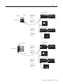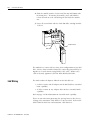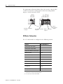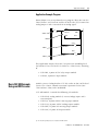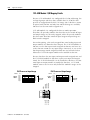
1
Remote I/O Adapter
Module
Catalog Number 1747-ASB
User Manual
Important User Information
Because of the variety of uses for the products described in this
publication, those responsible for the application and use of these
products must satisfy themselves that all necessary steps have been
taken to assure that each application and use meets all performance
and safety requirements, including any applicable laws, regulations,
codes and standards. In no event will Rockwell Automation be
responsible or liable for indirect or consequential damage resulting
from the use or application of these products.
Any illustrations, charts, sample programs, and layout examples
shown in this publication are intended solely for purposes of
example. Since there are many variables and requirements associated
with any particular installation, Rockwell Automation does not assume
responsibility or liability (to include intellectual property liability) for
actual use based upon the examples shown in this publication.
Allen-Bradley publication SGI-1.1, Safety Guidelines for the
Application, Installation and Maintenance of Solid-State Control
(available from your local Rockwell Automation office), describes
some important differences between solid-state equipment and
electromechanical devices that should be taken into consideration
when applying products such as those described in this publication.
Reproduction of the contents of this copyrighted publication, in whole
or part, without written permission of Rockwell Automation, is
prohibited.
Throughout this publication, notes may be used to make you aware of
safety considerations. The following annotations and their
accompanying statements help you to identify a potential hazard,
avoid a potential hazard, and recognize the consequences of a
potential hazard:
WARNING
!
ATTENTION
!
IMPORTANT
Identifies information about practices or
circumstances that can cause an explosion in a
hazardous environment, which may lead to personal
injury or death, property damage, or economic loss.
Identifies information about practices or
circumstances that can lead to personal injury or
death, property damage, or economic loss.
Identifies information that is critical for successful
application and understanding of the product.
Allen-Bradley is a trademark of Rockwell Automation
Summary of Changes
Summary of Changes
The information below summarizes the changes to this manual since
the last printing as Publication 1747-6.13 - December 1996.
To help you find new information and updated information in this
release of the manual, we have included change bars as shown to the
right of this paragraph.
New Information
1
For This New Information
See Page
Updated table of compatible scanners
1-9
Updated table of compatible RIO adapters
1-9
Updated list of compatible modules
1-10
Added primary/complementary chassis
information for SW2
2-3
Clarified DIP SW setting
4-5
C-Tick certification
A-1
Publication 1747-UM006B-EN-P - June 2003
2
Summary of Changes
Publication 1747-UM006B-EN-P - June 2003
Table of Contents
Preface
Who Should Use this Manual- . . . . . . . . . . . . . . .
Purpose of this Manual . . . . . . . . . . . . . . . . . . . .
Contents of this Manual . . . . . . . . . . . . . . . . .
Related Documentation . . . . . . . . . . . . . . . . .
Terms and Abbreviations. . . . . . . . . . . . . . . . . . .
Common Techniques Used in this Manual . . . . . .
Rockwell Automation Support . . . . . . . . . . . . . . .
Your Questions or Comments on this Manual .
.
.
.
.
.
.
.
.
.
.
.
.
.
.
.
.
.
.
.
.
.
.
.
.
.
.
.
.
.
.
.
.
.
.
.
.
.
.
.
.
.
.
.
.
.
.
.
.
.
.
.
.
.
.
.
.
.
.
.
.
.
.
.
.
.
.
.
.
.
.
.
.
1
1
1
2
3
5
6
6
Chapter 1
Overview
1747-ASB Module Overview . . . . . . . . . . . . . . . . . . . . . . . 1-1
Remote I/O Overview . . . . . . . . . . . . . . . . . . . . . . . . . . . . 1-2
How The Scanner Interacts With Adapters . . . . . . . . . . 1-2
Scanner I/O Image Division . . . . . . . . . . . . . . . . . . . . . 1-4
Crossing Logical Rack Boundaries. . . . . . . . . . . . . . . . . 1-4
Creating More Than One Logical Device by
Crossing a Logical Rack Boundary . . . . . . . . . . . . . . . 1-5
Transferring Data With RIO Discrete and Block Transfers 1-6
RIO Discrete Transfer Example. . . . . . . . . . . . . . . . . . . 1-7
Physical and Logical RIO Link Specifications . . . . . . . . . 1-8
Extended Node Capability . . . . . . . . . . . . . . . . . . . . . . 1-8
Compatible RIO Scanners. . . . . . . . . . . . . . . . . . . . . . . 1-9
Compatible RIO Adapters . . . . . . . . . . . . . . . . . . . . . . . . . 1-9
Compatible Modules . . . . . . . . . . . . . . . . . . . . . . . . . . . . . 1-10
1747-ASB Module Feature . . . . . . . . . . . . . . . . . . . . . . . . . 1-10
Hardware Features. . . . . . . . . . . . . . . . . . . . . . . . . . . . 1-11
Status Display and LEDs. . . . . . . . . . . . . . . . . . . . . . . . 1-11
DIP Switches . . . . . . . . . . . . . . . . . . . . . . . . . . . . . . . . 1-11
RIO Link and Processor Restart Lockout Connector . . . . 1-13
Door Label . . . . . . . . . . . . . . . . . . . . . . . . . . . . . . . . . 1-13
Self-Locking Tabs. . . . . . . . . . . . . . . . . . . . . . . . . . . . . 1-13
Cable Tie Slots. . . . . . . . . . . . . . . . . . . . . . . . . . . . . . . 1-13
Chapter 2
Quick Start for Experienced Users Required Tools and Equipment . . . . . . . . . . . . . . . . . . . . . 2-1
Procedures .
SW1 . . .
SW2 . . .
SW3 . . .
i
.
.
.
.
.
.
.
.
.
.
.
.
.
.
.
.
.
.
.
.
.
.
.
.
.
.
.
.
.
.
.
.
.
.
.
.
.
.
.
.
.
.
.
.
.
.
.
.
.
.
.
.
.
.
.
.
.
.
.
.
.
.
.
.
.
.
.
.
.
.
.
.
.
.
.
.
.
.
.
.
.
.
.
.
.
.
.
.
.
.
.
.
.
.
.
.
.
.
.
.
.
.
.
.
.
.
.
.
.
.
.
.
.
.
.
.
.
.
.
.
.
.
.
.
.
.
.
.
.
.
.
.
.
.
.
.
.
.
.
.
2-2
2-3
2-3
2-3
Publication 1747-UM006B-EN-P - June 2003
ii
Table of Contents
Chapter 3
Addressing
Chassis Overview . . . . . . . . . . . . . . . . . . . . . . . . .
Slot Numbering. . . . . . . . . . . . . . . . . . . . . . . . . . .
Addressing I/O Modules . . . . . . . . . . . . . . . . . . . .
2-Slot Addressing . . . . . . . . . . . . . . . . . . . . . . .
2-Slot Addressing Considerations . . . . . . . . . . .
2-Slot Addressing Examples . . . . . . . . . . . . . . .
1-Slot Addressing . . . . . . . . . . . . . . . . . . . . . . .
1-Slot Addressing Considerations . . . . . . . . . . .
1-Slot Addressing Examples . . . . . . . . . . . . . . .
1/2-Slot Addressing . . . . . . . . . . . . . . . . . . . . .
1/2-Slot Addressing Considerations . . . . . . . . . .
1/2-Slot Addressing Examples. . . . . . . . . . . . . .
How I/O Module Images Are Mapped . . . . . . . . . .
How Discrete I/O Modules Are Mapped . . . . . .
How Specialty I/O Module Images Are Mapped
When Block Transfer Mode is Selected . . . . . . .
When Discrete Mode is Selected. . . . . . . . . . . .
.
.
.
.
.
.
.
.
.
.
.
.
.
.
.
.
.
.
.
.
.
.
.
.
.
.
.
.
.
.
.
.
.
.
.
.
.
.
.
.
.
.
.
.
.
.
.
.
.
.
.
.
.
.
.
.
.
.
.
.
.
.
.
.
.
.
.
.
.
.
.
.
.
.
.
.
.
.
.
.
.
.
.
.
.
.
.
.
.
.
.
.
.
.
.
.
.
.
.
.
.
.
3-1
3-2
3-2
3-4
3-5
3-6
3-7
3-8
3-9
3-10
3-11
3-12
3-13
3-13
3-14
3-14
3-15
Chapter 4
Configuration
Publication 1747-UM006B-EN-P - June 2003
DIP Switch Information . . . . . . . . . . . . . . . . . . . . . . . . . . . 4-1
DIP Switch SW1. . . . . . . . . . . . . . . . . . . . . . . . . . . . . . 4-2
Logical Group Number (SW1-7,8) . . . . . . . . . . . . . . . . . 4-4
DIP Switch SW2. . . . . . . . . . . . . . . . . . . . . . . . . . . . . . 4-4
Primary/Complementary Chassis (SW2-3) . . . . . . . . . . . 4-5
Reserved (SW2-4) . . . . . . . . . . . . . . . . . . . . . . . . . . . . 4-9
Special Image and Chassis Size Considerations . . . . . . . . . . 4-13
Not Enough 1747-ASB Module Image to Map All of the
Available Slots . . . . . . . . . . . . . . . . . . . . . . . . . . . . . . . 4-13
1747-ASB Image Size Exceeds Slot Requirements. . . . . . 4-14
One Slot of Pair is Present, and 1747-ASB Module Image is
Available for Both Slots . . . . . . . . . . . . . . . . . . . . . . . . 4-14
Both Slots Of A Pair Are Available But There Is Only Enough
1747-ASB Module Image Space Available For One Slot . 4-15
DIP Switch SW3. . . . . . . . . . . . . . . . . . . . . . . . . . . . . . 4-15
Processor Restart Lockout (SW3-2) . . . . . . . . . . . . . . . . 4-17
Addressing Mode (SW3-5,6) . . . . . . . . . . . . . . . . . . . . . 4-20
Specialty I/O Mode (SW3-7) . . . . . . . . . . . . . . . . . . . . . 4-21
I/O Module Keying (SW3-8) . . . . . . . . . . . . . . . . . . . . . 4-21
Switch Setting Summary . . . . . . . . . . . . . . . . . . . . . . . . . . 4-22
SW2 . . . . . . . . . . . . . . . . . . . . . . . . . . . . . . . . . . . . . . 4-22
SW3 . . . . . . . . . . . . . . . . . . . . . . . . . . . . . . . . . . . . . . 4-23
Table of Contents
iii
Chapter 5
Installation and Wiring
European Union Direct Compliance. . . . . .
EMC Directive . . . . . . . . . . . . . . . . . . .
Installing the1747-ASB Module . . . . . . . . .
Link Wiring. . . . . . . . . . . . . . . . . . . . . . . .
Correct Link Wiring . . . . . . . . . . . . . . .
Incorrect Link Wiring . . . . . . . . . . . . . .
Link Termination . . . . . . . . . . . . . . . . .
Wiring a Processor Restart Lockout Switch .
I/O Module Addressing Labels. . . . . . . . . .
Using a PLC as a Master . . . . . . . . . . . .
Using an SLC as a Master . . . . . . . . . . .
Octal Label Kit Installation. . . . . . . . . . . . .
Applying the Octal Filter Label . . . . . . .
Applying the Octal Door Label . . . . . . .
Octal Kit and I/O Module Information .
.
.
.
.
.
.
.
.
.
.
.
.
.
.
.
.
.
.
.
.
.
.
.
.
.
.
.
.
.
.
.
.
.
.
.
.
.
.
.
.
.
.
.
.
.
.
.
.
.
.
.
.
.
.
.
.
.
.
.
.
.
.
.
.
.
.
.
.
.
.
.
.
.
.
.
.
.
.
.
.
.
.
.
.
.
.
.
.
.
.
.
.
.
.
.
.
.
.
.
.
.
.
.
.
.
.
.
.
.
.
.
.
.
.
.
.
.
.
.
.
.
.
.
.
.
.
.
.
.
.
.
.
.
.
.
.
.
.
.
.
.
.
.
.
.
.
.
.
.
.
.
.
.
.
.
.
.
.
.
.
.
.
.
.
.
.
.
.
.
.
.
.
.
.
.
.
.
.
.
.
5-1
5-1
5-1
5-2
5-3
5-3
5-4
5-5
5-6
5-6
5-6
5-7
5-7
5-7
5-8
System Start-Up. . . . . . . . . . . . . . . . . . . . . . . . . . . . . . . .
Powerup and Initialization Sequences . . . . . . . . . . . . . . .
Save Mode. . . . . . . . . . . . . . . . . . . . . . . . . . . . . . . . .
Check Mode . . . . . . . . . . . . . . . . . . . . . . . . . . . . . . .
Normal Operation . . . . . . . . . . . . . . . . . . . . . . . . . . . . . .
Communication Exception . . . . . . . . . . . . . . . . . . . . . . .
Inhibit Condition . . . . . . . . . . . . . . . . . . . . . . . . . . . .
Remote Expansion Chassis Power Loss . . . . . . . . . . . . . .
Invalid RIO Link Transfers . . . . . . . . . . . . . . . . . . . . . . . .
RIO Discrete or Block Transfers To Empty or
Nonexistent Chassis Slots . . . . . . . . . . . . . . . . . . . . .
RIO Discrete Transfers To Block Transfer Chassis Slots
RIO Block Transfers To Discrete Chassis Slots . . . . . . .
Invalid Length RIO Block Transfers. . . . . . . . . . . . . . .
Testing the 1747-ASB Module . . . . . . . . . . . . . . . . . . . . .
I/O Module Insertion into a Slot . . . . . . . . . . . . . . . . .
I/O Module Removal from a Scanned Slot. . . . . . . . . .
I/O Module Removal from an Unscanned Slot. . . . . . .
.
.
.
.
.
.
.
.
.
6-1
6-1
6-2
6-2
6-3
6-3
6-4
6-6
6-6
.
.
.
.
.
.
.
.
6-6
6-7
6-7
6-7
6-7
6-9
6-9
6-10
Troubleshooting Introduction . . . . . . . . . . . . . . . . . . . . . .
Contacting Rockwell Automation . . . . . . . . . . . . . . . . . . . .
Status Operating Codes for Normal Operating Conditions . .
Error Codes for Error Conditions . . . . . . . . . . . . . . . . . . . .
DIP Switch Configuration Mismatch Fault Codes - Codes
1 and 2 . . . . . . . . . . . . . . . . . . . . . . . . . . . . . . . . . . . .
7-1
7-2
7-2
7-3
Chapter 6
Start-Up and Operation
Chapter 7
Troubleshooting
7-5
Publication 1747-UM006B-EN-P - June 2003
iv
Table of Contents
I/O Module Configuration Mismatch
Fault Codes - Code 3 . . . . . . . . . . . . . . . . . . . . . . . . . . 7-7
I/O Runtime Fault Codes - Code 4 . . . . . . . . . . . . . . . . 7-8
Chapter 8
Application Examples
Basic SLC 500 Example Using and RIO Scanner
RIO Device Configuration . . . . . . . . . . . . .
SLC Processor Image . . . . . . . . . . . . . . . . .
1747-ASB Module Configuration Details . . .
1747-ASB Module I/O Mapping Details. . . .
RIO Address Label Examples . . . . . . . . . . .
Application Example Program . . . . . . . . . .
Basic SLC 500 Example Using and RIO Scanner
RIO Device Configuration . . . . . . . . . . . . .
SLC Processor Image . . . . . . . . . . . . . . . . .
1747-ASB Module 1 Configuration Details . .
1747-ASB Module 2 Configuration Details . .
1747-ASB Module 1 I/O Mapping Details . .
1747-ASB Module 2 I/O Mapping Details . .
RIO Address Label Examples . . . . . . . . . . .
Application Example Program . . . . . . . . . .
PLC-5 Example . . . . . . . . . . . . . . . . . . . . . . . .
RIO Device Configuration . . . . . . . . . . . . .
PLC Processor Image . . . . . . . . . . . . . . . . .
1747-ASB Module 1 Configuration Details . .
1747-ASB Module 2 Configuration Details . .
1747-ASB Module 1 I/O Mapping Details . .
1747-ASB Module 2 I/O Mapping Details . .
RIO Address Label Examples . . . . . . . . . . .
Application Example Program . . . . . . . . . .
Appendix A
Specifications
Appendix B
Differences Between the
1747-ASB Module and the
1771-ASB Series C Module
Appendix C
DIP Switch and Address
Configuration Worksheets
Index
Publication 1747-UM006B-EN-P - June 2003
.
.
.
.
.
.
.
.
.
.
.
.
.
.
.
.
.
.
.
.
.
.
.
.
.
.
.
.
.
.
.
.
.
.
.
.
.
.
.
.
.
.
.
.
.
.
.
.
.
.
.
.
.
.
.
.
.
.
.
.
.
.
.
.
.
.
.
.
.
.
.
.
.
.
.
.
.
.
.
.
.
.
.
.
.
.
.
.
.
.
.
.
.
.
.
.
.
.
.
.
.
.
.
.
.
.
.
.
.
.
.
.
.
.
.
.
.
.
.
.
.
.
.
.
.
.
.
.
.
.
.
.
.
.
.
.
.
.
.
.
.
.
.
.
.
.
.
.
.
.
.
.
.
.
.
.
.
.
.
.
.
.
.
.
.
.
.
.
.
.
.
.
.
.
.
.
.
.
.
.
.
.
.
.
.
.
.
.
.
.
.
.
.
.
.
.
.
.
.
.
.
.
.
.
.
.
.
.
.
.
.
.
.
.
.
.
.
.
.
.
.
.
.
.
.
8-1
8-2
8-3
8-4
8-4
8-5
8-7
8-7
8-9
8-10
8-10
8-11
8-12
8-12
8-13
8-15
8-16
8-17
8-18
8-19
8-20
8-21
8-22
8-23
8-24
Preface
Read this preface to familiarize yourself with the rest of the manual.
This preface covers the following topics:
•
•
•
•
•
Who Should Use this
Manual-
who should use this manual
the purpose of this manual
terms and abbreviations
conventions used in this manual
Rockwell Automation support
Use this manual if you are responsible for designing, installing,
programming, or troubleshooting control systems that use
Allen-Bradley small logic controllers.
You should have a basic understanding of PLC® and SLC®500
products. You should understand programmable controllers and be
able to interpret the ladder logic instructions required to control your
application. If you do not, contact your local Allen-Bradley®
representative for information on available training courses before
using this product.
Purpose of this Manual
This manual is a learning and reference guide for the remote I/O
adapter module. It describes the procedures you use to address,
configure, install, and operate the 1747-ASB remote I/O adapter
module.
Contents of this Manual
Chapter
1
Title
Contents
Preface
Describes the purpose, background, and scope of
this manual. Also specifies the audience for
whom this manual is intended.
1
Overview
Explains and illustrates the theory behind the
1747-ASB module's operation. Covers hardware
and software features, compatible devices, and
setup.
2
Quick Start for
Experienced Users
Serves as a Quick Start Guide for the 1747-ASB
module.
3
Addressing
Gives a chassis overview, and explains slot
numbering, I/O module image mapping, 2-slot,
1-slot, and 1/2-slot addressing.
Publication 1747-UM006B-EN-P - June 2003
2
Preface
4
Configuration
Contains DIP switch information, and shows odd
size chassis and image conditions.
5
Installation and
Wiring
Provides installation procedures and wiring
guidelines.
6
Start-up and
Operation
Explains powerup and initialization sequences,
normal operation, communication exceptions,
remote expansion power loss, invalid RIO link
transfers, and testing the 1747-ASB module.
7
Troubleshooting
Shows how to interpret and correct problems
with your 1747-ASB module.
8
Application Examples
Examines both SLC 500 and PLC-5/40t
applications using a 1747-ASB module. Gives
examples of the ladder programming necessary
to achieve the described result.
Appendix A
Specifications
Contains 1747-ASB and RIO link specifications,
as well as throughput information.
Appendix B
Differences Between
the 1747-ASB and
1771-ASB Series C
Modules
Provides a point-by-point comparison of the 1747
and 1771 ASB modules.
Appendix C
Worksheets
Contains worksheets for setting the 1747-ASB
module's DIP switches and addressing remote
I/O modules with an SLC processor.
Related Documentation
The following documents contain additional information concerning
Allen-Bradley SLCt and PLC products. To obtain a copy, contact your
local Allen-Bradley office or distributor.
For
Read This Document
Document
Number
An overview of the SLC 500 family of products
SLC 500 System Overview
1747-SO001
A description on how to install and use your Modular
SLC 500 programmable controller
Installation & Operation Manual for Modular
Hardware Style Programmable Controllers
User Manual
1747-UM011
Information regarding the use of a 1747-KE module as a
communications interface
DH-485/RS-232C Interface Module User
Manual
1747-6.12
Information regarding the use of the 1747-DCM as a remote
I/O device
Direct Communication Module User Manual
1747-6.8
Publication 1747-UM006B-EN-P - June 2003
Preface
Information regarding the use of the 1747-SN SLC RIO
scanner
RIO Scanner User Manual
1747-6.6
Information regarding the use of analog modules with the
SLC 500 system
SLC 500 Analog I/O Modules User Manual
1746-6.4
Information regarding programming your BASIC module
SLC 500 BASIC Language Reference
1746-RM001
In-depth information on grounding and wiring Allen-Bradley
programmable controllers
Allen-Bradley Programmable Controller
Grounding and Wiring Guidelines
1770-4.1
A description on how to install a PLC-5r system
PLC-5 Family Programmable Controllers
Hardware Installation Manual
1785-6.6.1
A description of important differences between solid-state
programmable controller products and hard-wired
electromechanical devices
Application Considerations for Solid-State
Controls
SGI-1.1
An article on wire sizes and types for grounding electrical
equipment
National Electrical Code
Published by the
National Fire
Protection
Association of
Boston, MA.
A glossary of industrial automation terms and abbreviations
Allen-Bradley Industrial Automation Glossary
AG-7.1
3
The following terms and abbreviations are specific to this product.
For a complete listing of Allen-Bradley terminology, refer to the
Allen-Bradley Industrial Automation Glossary, Publication Number
AG-7.1.
Terms and Abbreviations
Adapter - Any physical device that is a slave on the RIO link.
Adapter Image - That portion of the scanner image assigned to an
individual adapter. You configure the adapter image by assigning it a
starting logical rack number, starting logical group number and the
number of logical groups it uses. In the case of the 1747-ASB module,
this is referred to as the 1747-ASB module image.
ASB Module - The Catalog Number 1747-ASB Remote I/O Adapter
Module. The 1747-ASB module is an adapter.
ASB Module Chassis - The chassis directly controlled by the
1747-ASB module. This includes the remote chassis and (if installed)
two remote expansion chassis.
Discrete I/O Module - An I/O module used to sense or control
two-state (ON/OFF) devices.
Inhibit - A function by which the scanner stops communicating with
a logical device. The logical device will consider itself inhibited if it
Publication 1747-UM006B-EN-P - June 2003
4
Preface
does not receive communications from the scanner within a certain
period of time.
I/O Module - Any 1746 or 1747 I/O module that is supported by the
1747-ASB module.
Local Expansion Chassis - A chassis that is connected to a local SLC
chassis using a 1747-C9 (91.4 cm [36 in.]) or 1747-C7 (15.2 cm [6 in.])
cable.
Local PLC Chassis - The 1771 chassis that contains a PLC processor
and scanner.
Local SLC Chassis - The chassis that contains the SLC processor and
scanner.
Logical Device - Any portion of a logical rack that is assigned to a
single adapter. Adapters may appear as more than one logical device.
Logical Group - A logical group consists of one input and one output
word within a logical rack. A word consists of 16 bits, each bit
represents one terminal on a discrete I/O module.
Logical Rack - A fixed section of the scanner image comprised of
eight input words and eight output words.
Logical Slot - A logical slot consists of one input and one output byte
within a logical group. A byte consists of 8 bits, each bit represents
one terminal on a discrete I/O module.
PLC Chassis - A physical PLC rack that houses 1771 I/O modules and
PLC processors.
Remote Chassis - The chassis containing a 1747-ASB module and
connected to the local SLC or PLC chassis via the RIO link.
Remote Expansion Chassis - A chassis that is connected to a remote
chassis using a 1747-C9 (91.4 cm [36 in.]) or 1747-C7
(15.2 cm [6 in.]) cable.
Reset, Adapter Decide - Commands sent by the scanner to a logical
device during an RIO discrete transfer. These commands instruct the
logical device to reset all of its discrete outputs if hold last state is not
selected, or to hold all of its discrete outputs in their last state if hold
last state is selected.
Reset, Adapter Reset - Commands sent by the scanner to a logical
device during an RIO discrete transfer. These commands instruct the
logical device to reset all of its discrete outputs regardless of the hold
last state selection.
Publication 1747-UM006B-EN-P - June 2003
Preface
5
RIO Block Transfer - The exchange of up to 64 words of data
between the scanner and adapter. RIO block transfers only occur if
you program them in your processor control program. The 1747-ASB
module supports a block transfer of up to 8 words.
RIO Discrete Transfer - The exchange of image data between the
scanner and adapter. RIO discrete transfers occur continuously
whenever the scanner and adapter are communicating on the RIO
link.
RIO Link - An Allen-Bradley communication system supporting
high-speed serial transfer of Remote I/O (RIO) control information.
This link consists of one master one or more slaves.
Scanner - The communication master on the RIO link.
Scanner Image - The data table area within the scanner, used to
exchange I/O information between the scanner and all the adapters
on the RIO link. The scanner image is a portion of the SLC or PLC
processor image.
SLC Chassis - A physical SLC rack that houses SLC processors, 1746
and 1747 I/O modules.
Slot - The physical location in any chassis used to insert I/O modules.
Specialty I/O Module - An I/O module other than a discrete I/O
module (e.g., an analog module).
The following conventions are used throughout this manual:
Common Techniques Used
in this Manual
• Bulleted lists such as this one provide information, not
procedural steps.
• Numbered lists provide sequential steps or hierarchical
information.
• Italic type is used for emphasis.
• Text in this font indicates words or phrases you should type.
Allen-Bradley offers support services worldwide, with over 75
Sales/Support Offices, 512 authorized Distributors and 260 authorized
Systems Integrators located throughout the United States alone, plus
Allen-Bradley representatives in every major country in the world.
Publication 1747-UM006B-EN-P - June 2003
6
Preface
Rockwell Automation
Support
Before you contact Rockwell Automation for technical assistance, we
suggest you please review the troubleshooting information contained
in this publication first.
If the problem persists, call your local Rockwell Automation
representative or contact Rockwell Automation in one of the following
ways:
Phone
Internet
United
States/Canada
1.440.646.5800
Outside United
States/Canada
You can access the phone number for your
country via the Internet:
1. Go to http://www.ab.com
2. Click on Product Support
(http://support.automation.rockwell.com)
3. Under Support Centers, click on Contact
Information
⇒
1. Go to http://www.ab.com
2. Click on Product Support
(http://support.automation.rockwell.com)
Your Questions or Comments on this Manual
If you find a problem with this manual, please notify us of it.
If you have any suggestions for how this manual could be made more
useful to you, please contact us at the address below:
Rockwell Automation
Automation Control & Information Group
Technical Communication, Dept. 602V
P.O. Box 2086
Milwaukee, WI 53201-208
Publication 1747-UM006B-EN-P - June 2003
Chapter
1
Overview
This chapter presents:
•
•
•
•
•
1747-ASB Module
Overview
1747-ASB module overview
remote I/O overview
compatible devices
1747-ASB module features
setup and operational overview
The 1747-ASB module is an SLC 500 single-slot, RIO communication
link module. It occupies the first slot (slot 0) of a 1746 remote chassis,
where the SLC processor normally resides.
The 1747-ASB module is an adapter, or slave, on the RIO link, and the
master of the remote chassis and remote expansion chassis it is
installed in. Remote expansion chassis are optional. It acts as a
gateway between the scanner and the I/O modules residing in the
remote chassis and remote expansion chassis. The 1747-ASB module
maps the image of the I/O modules in its remote chassis and remote
expansion chassis directly to the SLC or PLC processor image.
Output data is sent from the scanner of either the SLC or PLC local
chassis to the 1747-ASB module across the RIO link. This data is
automatically transferred to the output modules across the chassis
backplane by the 1747-ASB module. Inputs from the input modules
are collected via the backplane by the 1747-ASB module and sent
back to the scanner across the RIO link. No user programming of the
1747-ASB module is necessary.
1747-ASB Module
Supervisory SLC (or PLC)
Remote Chassis Remote Expansion Chassis
RIO Link
1747-ASB Module
Outputs to
Modules
Inputs to
Modules
Remote Chassis
1747-ASB Module
Remote Chassis
1
Remote Expansion Chassis
Publication 1747-UM006B-EN-P - June 2003
1-2
Overview
To better understand the use of the 1747-ASB module, you should
have an understanding of the RIO link. The RIO link is an
Allen-Bradley communications system supporting high-speed transfer
of control information. An RIO link consists of a single master device
and one or more slave devices. The master device is referred to as the
scanner. The slave devices are referred to as adapters (such as the
1747-ASB module).
Remote I/O Overview
RIO scanners and adapters work together to serially communicate PLC
or SLC processor data to remotely located I/O devices. PLC and SLC
processors exchange inputs and outputs with scanners. Scanners
exchange inputs and outputs with adapters located on the RIO link.
The adapter's control is based on the adapter type.
How The Scanner Interacts With Adapters
The scanner's function is to continuously scan the adapters on the RIO
link in a consecutive manner. The scan consists of one or more RIO
discrete transfers to each adapter on the RIO link.
RIO discrete transfers consist of the scanner sending output image
data and communication commands to the adapter that instruct the
adapter on how to control its output. (These include run, reset,
adapter reset, and reset decide commands.) The adapter responds by
sending input data to the scanner. The scanner performs as many RIO
discrete transfers as necessary to update the entire adapter image. If
RIO discrete transfers do not occur, data is not exchanged between
the scanner and adapter.
IMPORTANT
Publication 1747-UM006B-EN-P - June 2003
RIO discrete transfers are asynchronous with the
processor scan.
Overview
1-3
1747-ASB Module
Processor
Scanner
RIO Discrete
Transfers with
Adapter 1
Remote Chassis Remote Expansion Chassis
SLC Local Chassis
RIO Link
RIO Discrete
Transfers with
Adapter 2
RediPANEL
1747-ASB Module
RIO Discrete
Transfers with
Adapter 3
Remote Chassis Remote Expansion Chassis
RIO Discrete
Transfers with
Adapter 4
RediPANEL
1747-ASB Module
Processor/Scanner
RIO Discrete
Transfers with
Adapter 1
PLC Local Chassis
RIO Link
Remote Chassis Remote Expansion Chassis
RIO Discrete
Transfers with
Adapter 2
RediPANEL
1747-ASB Module
RIO Discrete
Transfers with
Adapter 3
Remote Chassis Remote Expansion Chassis
RIO Discrete
Transfers with
Adapter 4
Publication 1747-UM006B-EN-P - June 2003
1-4
Overview
Scanner I/O Image Division
The scanner allows each adapter to use a fixed amount (user defined)
of the scanner's input and output image. Part of the processor's image
is used by local I/O, the other portion is used by the scanner for
remote I/O. For a PLC-5, logical rack 0 is dedicated for local I/O.
The scanner's remote I/O image is divided into logical racks and
further divided into logical groups. A full logical rack consists of eight
input and eight output image words. A logical group consists of one
input and one output word in a logical rack. Each logical group is
assigned a number from 0 to 7. The number of racks available for
remote I/O depends on the scanner you are using.
Local I/O
Logical Rack 0
Remote I/O
(Scanner
Image)
Logical Rack 1
Logical Rack 2
Logical Rack 3
Logical Group 0
Logical Group 7
Processor I/O
Image
Scanner I/O
Image
Adapter
Image
The scanner image also contains the image of each adapter on the
RIO link. The adapter is assigned a portion of the scanner image,
which is referred to as the adapter image.
Crossing Logical Rack Boundaries
Adapter image size is expressed in an even number of groups. For
example, the 1747-ASB module image can be any size between 2
logical groups and 32 logical groups (4 logical racks), in 2 logical
group increments.
If the adapter's image size is greater than 8 logical groups, the image
crosses logical rack boundaries. If an adapter's image size is less than
8 logical groups, it too can cross a logical rack boundary depending
upon the starting logical group number. The significance of crossing
logical rack boundaries is discussed in the next section.
Publication 1747-UM006B-EN-P - June 2003
Overview
Scanner Input or Output Image
Bit Number (Octal)
Bit Number (Decimal)
Logical
Rack 0
Logical
Rack 1
17
10 7
0
15
8 7
0
Group 0
Group 1
Group 2
Group 3
Group 4
Group 5
Group 6
Group 7
Group 0
Group 1
Group 2
Group 3
Group 4
Group 5
Group 6
Group 7
Scanner Input or Output Image
Bit Number (Octal)
Bit Number (Decimal)
Adapter
Image
Logical
Rack 0
Logical
Rack 1
Adapter image is 12 logical groups in size and
crosses a logical rack boundary due to its size.
IMPORTANT
1-5
Group 0
Group 1
Group 2
Group 3
Group 4
Group 5
Group 6
Group 7
Group 0
Group 1
Group 2
Group 3
Group 4
Group 5
Group 6
Group 7
17
10 7
0
15
8 7
0
Adapter
Image
Adapter image is 6 logical groups in size and crosses a logical
rack boundary due to its starting logical group number.
.
Due to SLC and PLC addressing differences, when
the 1747-ASB module is used with an SLC processor,
the image bit numbers are 0 to 7, 8 to 15 decimal.
When the 1747-ASB module is used with a PLC
processor, the image bit numbers are 0 to 7, 10 to 17
octal. The I/O image figures, like the two above,
indicate the type of image bit numbers used (octal,
decimal, or both) throughout this manual.
Creating More Than One Logical Device by Crossing a Logical
Rack Boundary
RIO discrete transfers occur on a logical device basis, not an adapter
basis. A logical device is any portion of a logical rack that is assigned
to a single adapter.
When an adapter's image is more than one logical device, the scanner
sees the single adapter as multiple adapters on the RIO link. The
scanner communicates with each logical device independently, even if
the logical devices are all assigned to one adapter. If an adapter
image is more than one logical device, the following is true:
Not all of the adapter image is updated by the scanner at the same
time. The number of logical devices determines the number of RIO
discrete transfers that are needed to update the entire adapter image.
Publication 1747-UM006B-EN-P - June 2003
1-6
Overview
The adapter may receive different communication commands for each
logical device. In this case, the adapter decides which command it
responds to.
Scanner Input or Output Image
In this example, two RIO
discrete transfers are
required for the scanner to
update the adapter image
containing two logical
devices.
Bit Number (Octal)
17
10 7
0
Bit Number (Decimal)
15
8 7
0
Logical
Rack 0
Logical
Rack 1
Group 0
Group 1
Group 2
Group 3
Group 4
Group 5
Group 6
Group 7
Group 0
Group 1
Group 2
Group 3
Group 4
Group 5
Group 6
Group 7
Logical
Device
Adapter
Image
Logical
Device
To understand how an adapter's logical devices are assigned, use
appendix D to determine the address configuration of your remote
I/O modules. You may then want to reassign certain adapters so their
images do not cross logical rack boundaries, allowing the scanner to
update their images in one RIO discrete transfer.
IMPORTANT
The 1747-ASB module always functions as one
adapter on the RIO link, even though it may contain
more than one logical device. For example, the
1747-ASB module does not begin normal operation
until all of its logical devices are receiving RIO
discrete transfers from the scanner.
Transferring Data With RIO Discrete and Block Transfers
Input and output image data and command information is quickly
exchanged between a scanner and adapter using RIO discrete
transfers. RIO discrete transfers are the simplest way a scanner and
adapter communicate with each other. RIO discrete transfers, which
are transparent to the user, consist of the scanner sending the output
image data to the adapter, and the adapter transmitting input data to
the scanner. Each RIO discrete transfer also contains scanner
commands for the adapter.
Publication 1747-UM006B-EN-P - June 2003
Overview
1-7
RIO block transfers are initiated by a special command from the PLC
processor, typically when large amounts of data must be exchanged
with one specialty I/O module. Block transfers use the basic RIO
discrete transfer mechanism of the RIO link. However, the actual
transfer of data occurs asynchronous to the discrete transfers. It is
possible for several discrete transfers to occur before a block transfer
is processed.
RIO Discrete Transfer Example
This example illustrates how additional discrete transfers are required
when an adapter image crosses logical rack boundaries. It consists of
one scanner and three adapters. Adapter 1 requires one RIO discrete
transfer from the scanner to update its entire image. Adapter 2
requires two RIO discrete transfers to update its image. Adapter 3
requires three RIO discrete transfers to update its image.
Scanner Input or Output Image
Bit Number (Octal)
Bit Number (Decimal)
17
10 7
0
15
8 7
0
Group 0
Logical
Rack 0
Adapter 1
Logical Device 1
Adapter 2
Logical Device 1
Logical
Rack 1
Adapter 2
Logical Device 2
Adapter 3
Logical Device 1
Logical
Rack 2
Logical
Rack 3
Adapter 3
Logical Device 2
Adapter 3
Logical Device 3
Group 1
Group 2
Group 3
Group 4
Group 5
Group 6
Group 7
Group 0
Group 1
Group 2
Group 3
Group 4
Group 5
Group 6
Group 7
Group 0
Group 1
Group 2
Group 3
Group 4
Group 5
Group 6
Group 7
Group 0
Group 1
Group2
Group 3
Group 4
(1)
(2)
1747-ASB Module
to scanner
Adapter 1 Configured As:
Starting Logical Rack: 0
Starting Logical Group: 0
Adapter Image Size: 6 logical groups
Adapter 2 Configured As:
Starting Logical Rack: 0
Starting Logical Group: 6
Adapter Image Size: 8 logical groups
Adapter 3 Configured As:
Starting Logical Rack: 1
Starting Logical Group: 6
Adapter Image Size: 18 logical groups
(3)
Group 5
Group 6
Group 7
(1) The scanner updates the adapter image in one RIO discrete transfer because the adapter image is contained
within one logical rack.
(2) The scanner updates the adapter image in two RIO discrete transfers because the adapter image crosses a
logical rack boundary making the adapter image appear as two logical devices.
(3) The scanner updates the adapter image in three RIO discrete transfers because the adapter image crosses two
logical rack boundaries making the adapter image appear as three logical devices.
Publication 1747-UM006B-EN-P - June 2003
1-8
Overview
Physical and Logical RIO Link Specifications
The maximum number of adapters that your scanner can
communicate with is determined by the scanner and adapter's
physical and logical specifications, as described below:
Physical Specifications are the maximum number of adapters that can
be connected to the scanner. For more information, see Extended
Node Capability below.
Logical Specifications for the scanner are the maximum number of
logical racks the scanner can address, how the logical racks can be
assigned, and whether the scanner can perform block transfers.
For adapters, logical specification refers to the maximum size of the
adapter's RIO image.
Extended Node Capability
Both scanners and adapters can have extended node capability.
Extended node capability allows you to use an 82 Ohm termination
resistor at both ends of the RIO link for all baud rates. Extended node
capability also allows for up to 32 adapters to be placed on the RIO
link.
Extended node capability can only be used if the scanner and all
adapters on the RIO link have extended node capability. The
1747-ASB module has extended node capability.
The tables on pages 1-10 and 1-11 provide lists of compatible RIO
scanners and adapters.
The 1747-ASB module is compatible with all Allen-Bradley scanners.
Scanners that do not support RIO block transfers do not work with all
of the I/O modules supported by the 1747-ASB module. For example,
the Catalog Number 1747-SN Series A, RIO Scanner does not work
with a Catalog Number 1746-BAS, BASIC module because the scanner
does not support RIO block transfer.
Publication 1747-UM006B-EN-P - June 2003
Overview
1-9
Compatible RIO Scanners
Refer to the appropriate scanner manual for details concerning
physical and logical specifications.
Catalog Number
Description
1771-SN(1)
Sub I/O scanner for Mini-PLC®-2 and PLC-5 families
1785-L11B(2)
PLC-5/11™ (in scanner mode)
1785-L20B(2)
PLC-5/20™ (in scanner mode)
1785-L30x(2)
PLC-5/30™ (in scanner mode)
1785-L40x(2)
PLC-5/40 (in scanner mode)
1785-L60x(2)
PLC-5/60™ (in scanner mode)
1747-SN(2)(3)
SLC Remote I/O Scanner
(1) Revision D or later.
(2) Extended node capability.
(3) Series A scanner does not have block transfer.
Compatible RIO Adapters
The 1747-ASB module can physically reside on the RIO link with any
other adapter. The following table lists the adapters available for use
with an RIO link.
Catalog Number
Description
1785-L30x(1)(2)
PLC-5/30 (in adapter mode)
1785-L40x(1)(2)
PLC-5/40 (in adapter mode)
1785-L60x(1)(2)
PLC-5/60 (in adapter mode)
1771-ASC
Remote I/O Adapter Module
1771-ASB(3)(4)
Remote I/O Adapter Module
1771-RIO
Remote I/O Interface Module
1771-DCM
Direct Communication Module
1747-DCM(1)
Direct Communication Module
2711-xx(1)
PanelView™ Terminal
1336-G2(1)
Remote I/O Adapter for 1336 AC Industrial Drives
1395-NA(1)
Remote I/O Adapter for 1395 DC Industrial Drives
1747-ASB(1)
Remote I/O Adapter Module
(1) Extended node capability.
(2) In adapter mode.
(3) Series A, B, and C.
(4) Extended node capability for Series B and C.
Publication 1747-UM006B-EN-P - June 2003
1-10
Overview
Compatible Modules
The 1747-ASB module supports all SLC 5/01 compatible I/O modules
(class 0 and 1). The following modules can be placed in the remote
chassis and remote expansion chassis:
• all discrete I/O modules
• all analog I/O modules
• BASIC Modules, Catalog Number 1746-BAS, -BAST
(SLC 5/01 mode)
• IMC 110 motion control module, Catalog Number 1746-HS
• Direct Communication Module, Catalog Number 1747-DCM
• Thermocouple/mV input modules, Catalog Number
1746-NT4, NT8
• RTD/Resistance Modules, Catalog Number 1746-NR4, NR8
• High Speed Counter Module, Catalog Number 1746-HSCE 2
1747-ASB Module Feature
The 1747-ASB module has the following features:
• communicates I/O data up to a maximum of 3040 meters
(10,000 feet)
• supports 57.6K, 115.2K, and 230.4K baud operation on the RIO
link
• supports any mix of 1746 discrete or analog I/O
• controls up to 30 slots using remote expansion chassis
• allows use of 2-slot, 1-slot, and 1/2-slot addressing
• allows for image sizes between 2 and 32 logical groups (user
selectable)
• incorporates enhanced operating status and troubleshooting
capability using three 7-segment displays
• provides non-volatile memory for convenient I/O module slot
keying
• provides discrete output module hold last state selection
• provides RIO link processor restart lockout selection
• incorporates extended node capability
• supports RIO block transfers and RIO discrete transfers for
analog and other specialty I/O modules
• supports complementary I/O on the RIO link
Publication 1747-UM006B-EN-P - June 2003
Overview
1-11
Hardware Features
The 1747-ASB module's hardware features are highlighted below.
Detailed installation, operation, and troubleshooting information is
contained in chapters 5, 6, and 7.
COMM LED
(Green)
FAULT LED
(Red)
DIP Switches
FRN
3
4
6
O
N
7
3
2
1
RESP
FAC 1M
O
N
HLS
PRL
5
MADE IN USA
ADDR
MODE
6
4
SW3
LAST CHA
SP MODE
7
KEY
OPERATING
TEMPERATURE
CODE T3C
8
RET
8
IMPORTANT:
INSTALL IN SLOT ZERO OF MODULAR CHASSIS ONLY
CURRENT REQUIREMENT: 375mA
6
5
R
IMAGE
SIZE
(LSB)
SA
RSV
(MSB)
4
IN
3
NC
SW2
LINE 2
BAUD
RATE
PRI/COMP
2
SHLD
1
LINE 1
LISTED IND. CONT. EQ.
FOR HAZ. LOC. A196
Manufacturing Test Plug
UL
8
CLASS 1, GROUPS A, B, C AND D, DIV. 2
7
Door
Label
R
5
LOGICAL
GROUP
SLC 500
REMOTE I/O ADAPTER MODULE
SER
3 4 5 6 7 8
2
SW1
LOGICAL
RACK
(LSB)
RIO Link and
Processor
Restart
Lockout
Connector
CAT
2
SERIAL NO.
O 1
N
3 4 5 6 7 8
3 4 5 6 7 8
2
2
(MSB)
1
Status Display
O 1
N
O 1
N
ST ATUS
SW1
COMM F AUL T
SW2
SW3
ADAPTER
1747–ASB
Cable Tie Slots
Self-Locking Tab
Status Display and LEDs
The Status Display provides alphanumeric status of the 1747-ASB
module and RIO link. When combined with the COMM and FAULT
LEDs, they are very effective troubleshooting tools.
DIP Switches
The 1747-ASB module's three DIP switches allow you to configure the
following items:
• Starting Logical Rack Number (Logical Rack) - is the
1747-ASB module's starting logical rack number in the scanner's
image.
• Starting Logical Group Number (Logical Group) - is the
1747-ASB module's starting logical group number within the
scanner's image.
Publication 1747-UM006B-EN-P - June 2003
1-12
Overview
• Baud Rate (Baud Rate) - is the 1747-ASB module's RIO link
communication rate. The baud rate must be the same for all
adapters on the RIO link.
• Primary/Complementary SLC Chassis (PRI/COMP) determines whether the 1747-ASB module appears to the
scanner as a primary or complementary chassis.
• Adapter Image Size (IMAGE SIZE) - indicates the I/O image
size to be reserved for the adapter. It can be any size between 2
and 32 groups in two logical group increments.
• Hold Last State (HLS) - determines whether the discrete output
modules are held in their last state when:
– RIO link communication with the 1747-ASB module is lost.
– The scanner inhibits the 1747-ASB module.
– The scanner sends Reset, Adapter Decide commands to the
1747-ASB module.
• Processor Restart Lockout (PRL) - determines whether the
1747-ASB module automatically resumes RIO link
communications if communication is lost and then restored.
• Link Response Time (RESP) - selects restricted or unrestricted
RIO link response time.
• Last Chassis (LAST CHA) - When the 1747-ASB module is used
with a PLC-2 or PLC-5, this switch indicates to the scanner that
the 1747-ASB module is the last adapter mapped into the
1747-ASB module's highest logical rack.
• Addressing Mode (ADDR MODE) - determines the 1747-ASB
module's remote chassis and remote expansion chassis
addressing mode. 2-slot, 1-slot, and 1/2-slot is available.
• Specialty I/O Mode (SP MODE) - determines whether the
1747-ASB module discretely maps or block transfer maps
specialty I/O modules in its remote chassis and remote
expansion chassis.
• I/O Module Keying (KEY) - determines if the 1747-ASB
module saves its current I/O module and DIP switch
configuration to its non-volatile memory, or if the 1747-ASB
module compares the current I/O module and DIP switch
configuration to the one saved in its non-volatile memory.
Publication 1747-UM006B-EN-P - June 2003
Overview
1-13
RIO Link and Processor Restart Lockout Connector
The 6-pin male connector attaches the 1747-ASB module to the RIO
link and processor restart lockout device.
Door Label
The door label provides DIP switch and wiring information.
Self-Locking Tabs
Self-locking tabs secure the module in the rack. No tools are
necessary to install or remove a module.
Cable Tie Slots
Cable tie slots can be used to secure the wiring cable to the module.
Publication 1747-UM006B-EN-P - June 2003
1-14
Overview
Publication 1747-UM006B-EN-P - June 2003
Chapter
2
Quick Start for Experienced Users
This chapter helps you to get started using the 1747-ASB module. We
base the procedures here on the assumption that you have an
understanding of PLC and SLC 500 products, as well as the RIO link.
You should understand electronic process control and be able to
interpret the ladder logic instructions required to generate the
electronic signals that control your application.
Because it is a start-up guide for experienced users, this chapter does
not contain detailed explanations about the procedures listed. It does,
however, reference other chapters in this book where you can get
more detailed information.
If you have any questions, or are unfamiliar with the terms used or
concepts presented in the procedural steps, always read the
referenced chapters before trying to apply the information.
This chapter:
•
•
•
•
•
tells you what tools and equipment you need
lists preliminary considerations
describes when to address and configure the module
explains how to install and wire the module
discusses system power-up procedures
Have the following tools and equipment ready:
Required Tools and
Equipment
1
• medium blade screwdriver
• (2) 1/2 watt terminating resistors (See chapter 5, Installation
and Wiring, for correct size.)
• an adequate length of RIO communication cable (Belden
9463) for your specific application (See Chapter 5 Installation
and Wiring, for maximum cable distances.)
Publication 1747-UM006B-EN-P - June 2003
2-2
Quick Start for Experienced Users
Procedures
1.
Check the contents of shipping box.
Reference
Unpack the shipping box making sure that the contents include:
• Remote I/O adapter module (Catalog Number 1747-ASB)
• user manual (Publication 1747-6.13)
If the contents are incomplete, call your local Rockwell Automation representative for
assistance.
-
2.
Reference
Ensure your chassis supports placement of the 1747-ASB module.
Check to see that your chassis supports placement of the adapter module by:
• reviewing the power requirements of your system (The adapter consumes 600 mA
at 5VDC.)
• calculating the total load on the system power supply using the procedure described
in Appendix B
3.
Choose the type of slot addressing you will use.
Appendix A
(Specifications)
Appendix B
(Understanding
your
SLC 500/1746
Control System)
Reference
Select 1747-ASB addressing (i.e., 2-slot, 1-slot, or 1/2-slot). A configuration worksheet is
included in appendix D to assist you in 1747-ASB image table addressing.
Chapter 3
(Addressing)
Important: Due to SLC and PLC addressing differences, when the 1747-ASB module is used
with an SLC processor, the image bit numbers are 0 to 7, 8 to 15 decimal. When the
1747-ASB module is used with a PLC processor, the image bit numbers are 0 to 7, 10 to 17
octal.
Appendix D
(DIP Switch and
Address
Configuration
Worksheets)
4.
Reference
Configure the module using the DIP switches.
Set the DIP switches (located on the printed circuit board) to the desired setting. A
worksheet is included in appendix D to assist you in DIP switch configuration.
Chapter 4
(Configuration)
Appendix D
(DIP Switch and
Address
Configuration
Worksheets)
Publication 1747-UM006B-EN-P - June 2003
Quick Start for Experienced Users
SW1
SW1
O
N
1
2
3 4 5 6 7 8
ON
OFF
Logical Rack Number Bit 5 (MSB)
Logical Rack Number Bit 4
Logical Rack Number Bit 3
Logical Rack Number Bit 2
Logical Rack Number Bit 1
Logical Rack Number Bit 0 (LSB)
Logical Group Number Bit 1 (MSB)
Logical Group Number Bit 0 (LSB)
Logical Rack Number
For details, see page 4-2.
Logical Group Number
7
ON
ON
OFF
OFF
8
ON
OFF
ON
OFF
Group
0 (default)
2
4
6
2
ON
OFF
ON
OFF
Baud Rate
57.6K (default)
115.2K
230.4K
INVALID
SW2
SW2
Baud Rate
O
N
1
2
3 4 5 6
ON
OFF
2-3
7
8
Baud Rate Bit 1 (MSB)
Baud Rate Bit 0 (LSB)
Reserved
Primary/Complementary Chassis
ASB Module Image Size Bit 3 (MSB)
ASB Module Image Size Bit 2
ASB Module Image Size Bit 1
ASB Module Image Size Bit 0 (LSB)
1
ON
ON
OFF
OFF
• Primary/Complementary Chassis
ON=Primary
OFF=Complementary (Default)
• 1747-ASB Module Image Size
For details, see page 4-9.
SW3
SW3
O
N
• Hold Last State
ON=Hold Last State
OFF = Do Not Hold Last State (default)
• Processor Restart Lockout
ON = Automatic Restart (default)
OFF = Processor Lockout
• Link Response
ON = Restricted 9 (default)
OFF = Unrestricted
• Last Chassis
ON = Not Last Chassis (default)
OFF = Last Chassis
• Addressing Mode
1
2
3 4 5 6 7
ON
OFF
8
Hold Last State
Processor Restart Lockout
Link Response
Last Chassis/PLC –3 Backup
Addressing Mode Bit 1 (MSB)
Addressing Mode Bit 0 (LSB)
Specialty I/O Mode
I/O Module Keying
5
ON
ON
OFF
OFF
6
ON
OFF
ON
OFF
Address
Invalid
1-slot Addressing
1/2 slot Addressing
2-slot Addressing
• Specialty I/O Mode
ON = Discrete (default)
OFF = Block Transfer
• I/O Module Keying
ON = Save Mode (default)
OFF = Check Mode
Publication 1747-UM006B-EN-P - June 2003
2-4
Quick Start for Experienced Users
5.
Insert the 1747-ASB module into the chassis.
ATTENTION
!
Never insert, remove or wire modules with power
applied to the chassis or devices wired to the
module.
Reference
Chapter 5
(Installation and
Wiring)
Make sure system power is off; then insert the adapter module into slot 0 of your 1746
chassis.
Module Release
Card Guide
6.
Connect all RIO link devices.
Ensure that you:
• Daisy chain each RIO link device.
• Ground the shield drain wire to the nearest chassis mounting bolt.
• Connect the appropriate termination resistors on each end of the link.
Important: Do not connect anything to the NC (No Connect) terminal.
Publication 1747-UM006B-EN-P - June 2003
Reference
Chapter 5
(Installation and
Wiring)
Quick Start for Experienced Users
7.
(Optional) Wire a processor restart lockout switch.
ATTENTION
!
2-5
Reference
Cycling power on any 1747-ASB module chassis
removes the processor restart lockout condition
(SW-2) by reinitializing the 1747-ASB module.
Chapter 5
(Installation and
Wiring)
Use a momentary switch (Class 1, Division 2) to short terminals IN and RET together.
Important: Do not connect anything to the NC (No Connect) terminal.
LINE 1 (Blue wire)
SHLD (Shield wire)
LINE 2 (Clear wire)
NC (No Connect)
IN
RET
Momentary Switch
14 to 24 gauge wire
(maximum 5 feet)
8.
Attach the appropriate I/O Module Addressing Labels.
Reference
Attach the Remote PLC or Remote SLC label to the outside bottom of each I/O module in
your 1747-ASB chassis, as shown below. Fill out each label completely.
Chapter 5
(Installation and
Wiring)
Chapter 8
(Application
Examples)
INPUT
INPUT
0 –7
10 – 17
Rack Group(s)
I:
O:
Discrete
BT
Remote PLC R System
0 –7
8 – 15
Discrete
BT
Remote SLC R System
Remote PLC Label
Remote SLC Label
SN Slot
SN Word(s)
0 –7
Rack
I:
10 – 17
Group(s)
O:
Discrete
Remote PLC R System
BT
0 –7
8 – 15
SN Slot
SN Word(s)
BT
Discrete
Remote SLC
R
System
Publication 1747-UM006B-EN-P - June 2003
2-6
Quick Start for Experienced Users
9.
If using a PLC processor as a master, attach the octal labels.
The octal filter and door labels must be used when working with a PLC processor as a
master. A list of I/O modules that include an octal label kit can be found on page 5-8.
Adhere the octal labels over the existing decimal labels, as shown below.
Decimal Filter Label
Reference
Chapter 5
(Installation and
Wiring)
Octal Filter Label
INPUT
OCT AL
Octal Door Label
1746–XXXX
1746–XXXX (OCT AL)
Decimal Door Label
10.
Go through the system start-up procedure.
ATTENTION
!
Never insert, remove or wire modules with power
applied to the chassis or devices wired to the
module.
Follow the steps below:
1. Cycle power one last time in save mode (SW3-8 ON).
2. Remove power from the system.
3. Remove the 1747-ASB module and set SW3-8 to the OFF position (check mode).
4. Replace the 1747-ASB module in slot 0.
5. Apply power to your system.
Publication 1747-UM006B-EN-P - June 2003
Reference
Quick Start for Experienced Users
11.
Check that the module is operating correctly.
Reference
During normal operation (PLC or SLC in Run mode), the 1747-ASB module appears as shown
below:
ADAPTER
Status display
indicates a run
condition.
Chapter 6
(Start-Up and
Operation)
Chapter 7
(Troubleshooting)
COMM F AULT
Green COMM
LED is on.
2-7
Red F AULT
LED is off.
ST ATUS
Publication 1747-UM006B-EN-P - June 2003
2-8
Quick Start for Experienced Users
Publication 1747-UM006B-EN-P - June 2003
Chapter
3
Addressing
This chapter presents:
• slot numbering
• 2-slot, 1-slot, and 1/2-slot addressing
• how I/O module images are mapped
The 1747-ASB module controls 1 remote chassis and up to 2 remote
expansion chassis with a maximum of 30 slots. Currently, there are
four different types of chassis available.
Chassis Overview
4-Slot
7-Slot
Catalog Number 1746-A4
10-Slot
Catalog Number 1746-A10
Catalog Number 1746-A7
13-Slot
Catalog Number 1746-A13
The first chassis is referred to as the remote chassis. Up to two
additional chassis, referred to as remote expansion chassis, can be
connected to the remote chassis using a:
• 6 inch cable, Catalog Number 1746-C7
• 36 inch cable, Catalog Number 1746-C9
Each remote chassis and remote expansion chassis requires its own
power supply.
1
Publication 1747-UM006B-EN-P - June 2003
3-2
Addressing
IMPORTANT
A 1747-ASB module fault occurs if the remote
expansion chassis are not powered.
Catalog Number 1746-C9
36 inch cable
Catalog Number 1746-P1
Remote Chassis
Remote Expansion Chassis
Catalog Number 1746-P3
Catalog Number 1746-C7
Catalog Number 1746-P2
Remote Chassis
6 inch
cable
Remote Expansion Chassis
Catalog Number 1746-P2
Slot Numbering
The 1747-ASB module is capable of controlling 30 slots. When
expansion chassis are used, the 1747-ASB module treats all of the I/O
modules as if they are installed in a single chassis.
The remote chassis and remote expansion chassis slots are numbered
from 0 to 30. The 1747-ASB module must reside in slot 0. Slots
numbered 31 and above cannot be used.
IMPORTANT
Addressing I/O Modules
Publication 1747-UM006B-EN-P - June 2003
Installing modules in slots 31 and above causes a
1747-ASB module error.
SLC and PLC processors address the I/O modules residing in the
1747-ASB module chassis by logical rack and logical group. Before
using the 1747-ASB module, you should first understand slot
addressing and how each module's image is mapped into the
1747-ASB module's image.
Addressing
3-3
Slot addressing refers to how each chassis slot is assigned a specific
amount of the 1747-ASB module image. The amount depends on
which type of slot addressing you choose; 2-slot, 1-slot, and 1/2-slot
addressing is available, as shown below:
IMPORTANT
2-Slot
Addressing
Due to SLC and PLC addressing differences, when
the 1747-ASB module is used with an SLC processor,
the image bit numbers are 0 to 7, 8 to 15 decimal.
When the 1747-ASB module is used with a PLC
processor, the image bit numbers are 0 to 7, 10 to 17
octal.
Two slots are addressed as one logical group.
Input Image
Slot 2
Output Image
Slot 1
1-Slot
Addressing
Slot 2
Slot 1
One slot is addressed as one logical group.
Input Image
Output Image
Slot 1
1/2-Slot
Addressing
Slot 1
One slot is addressed as two logical groups.
Input Image
Output Image
Slot 1
Slot 1
Publication 1747-UM006B-EN-P - June 2003
3-4
Addressing
2-Slot Addressing
When the 1747-ASB module is configured for 2-slot addressing, the
processor addresses two chassis slots as one logical group. Each slot,
beginning with slot 1, is sequentially assigned one byte (8 bits) of the
1747-ASB module's input and output image. Each terminal on a
discrete I/O module installed in a slot is assigned a bit within the byte,
beginning with the least significant bit. 2-slot addressing is designed
to accommodate I/O modules whose image size is one byte or less.
Slot 1 is assigned to the low byte of the first logical
group of the 1747-ASB module ’s image, beginning
with bit 0 (the LSB).
Slot 1
Input Image
17
1 5 1 4 1 3 1 2 11 1 0
9
10 7
8 7
6
Output Image
5
4
3
2
0
1 0
Octal
Decimal
17
1 5 1 4 1 3 1 2 11 1 0
9
10
8
7
7
6
5
4
3
2
0
1
0
group 0
Octal
Decimal
group 0
Slot 1
Slot 1
Each terminal is assigned a bit,
beginning with the least significant bit.
Each terminal is assigned a bit,
beginning with the least significant bit.
Slot 2 is assigned to the high byte of the first
logical group of the 1747-ASB module’s
image, beginning with bit 8 decimal, 10 octal.
Slot 2
Input Image
17
1 5 1 4 1 3 1 2 11 1 0
9
10 7
8 7
6
Output Image
5
4
3
2
0
1 0
Octal
Decimal
17
1 5 1 4 1 3 1 2 11 1 0
group 0
Slot 2
Each terminal is assigned a bit,
beginning with the least significant bit.
Publication 1747-UM006B-EN-P - June 2003
9
10
8
7
7
6
5
4
3
2
0
1
0
Octal
Decimal
group 0
Slot 2
Each terminal is assigned a bit,
beginning with the least significant bit.
Addressing
3-5
To accommodate modules that require up to one word (16 bits) of
input and/or output image, the 1747-ASB module pairs slots
beginning with slot 1 (i.e., slot 1 is paired to slot 2, etc.). Slot pairing
combines the low and high byte into a one word input and output
image. This maximizes I/O image space, allowing you to install an
input module in one slot and an output module in the other, each
using up to 16 bits of the paired input and output images.
I
O
Slot 1
Paired
When a module is installed in slot 1 that requires one word of
input image, slot 1 uses the input image normally assigned to
slots 1 and 2. Slot 2, therefore, cannot use any of its input
image. However, slot 2 can now use the output image
normally assigned to slots 1 and 2, because slot 1 is not
using its portion of the output image.
Input Image
17
1 5 1 4 1 3 1 2 11 1 0
I = Input Module
O = Output Module
9
10 7
8 7 6
5
4
3
0
1
2
0
Octal
Decimal
Group 0
Slot 1
Slot Pair
I
O
Slot 1
When a module is installed in slot 2 that requires one word of
output image, slot 2 uses the output image normally
assigned to slots 1 and 2 (if slot 1 is not already using it).
The lesser slot number has priority over the greater.
Slot 2
Paired
Output Image
17
1 5 1 4 1 3 1 2 11 1 0
9
10
8
7
7
6
5
4
3
2
0
1
0
Octal
Decimal
Group 0
Slot 2
Slot 2
2-Slot Addressing Considerations
When the 1747-ASB module is configured for 2-slot addressing, you
can use 4-, 8-, 16-point, combination, and specialty I/O modules.
If it is necessary to use 16-point modules, like modules (i.e., two input
modules) cannot be installed as a pair. This is because each 16-point
module uses a full word in the image. For this reason you must pair
an input with an output module. 32-point modules cannot be used.
If the discrete mode is selected, specialty I/O modules with one word
or less of input and output image are discretely mapped such as the
1747-KE. Specialty I/O modules with two or more words of input or
output image are block transfer mapped.
If block transfer mode is selected, all specialty I/O modules are block
transfer mapped regardless of their image size.
The 1747-ASB module can block transfer map a maximum of eight
words.
Publication 1747-UM006B-EN-P - June 2003
3-6
Addressing
2-Slot Addressing Examples
The following example illustrates how to map modules requiring:
• one byte or less of input or output image
• one word of input or output image
I
I = Input Module
O = Output Module
I
I
O
1746 Slot Numbering 0
Slot Pair
1
2
O
3
1
4
2
I
O
5
6
I
I
O
7
3
Modules Requiring One Byte
In this example, the modules require one byte of input
or output image.
Input modules do not have to be paired with output
modules because, in the example to the right, only one
byte of input or output image is required.
To use image space more efficiently, slot pairing can b
used with 16-point I/O modules as shown below or
complementary I/O can be used. Refer to page 4-5.
I
O
8
9
10
4
11 12
5
17
15
10
8
Slot 2
Slot 4
Slot 6
Slot 8
Slot 10
Slot 12
Slot 14
Slot 16
Slot 18
7
7
0
0
I
O
13
6
1747-ASB Input Image
I
O
O
14 15 16
7
O
17
8
18
9
1747-ASB Output Image
Octal
Decimal
17
15
Slot 1
Slot 3
Slot 5
Slot 7
Slot 9
Slot 11
Slot 13
Slot 15
Slot 17
10
8
7
7
Slot 2
Slot 4
Slot 6
Slot 8
Slot 10
Slot 12
Slot 14
Slot 16
Slot 18
0
0
Slot 1
Slot 3
Slot 5
Slot 7
Slot 9
Slot 11
Slot 13
Slot 15
Slot 17
Octal
Decimal
Slot Pair 1
Slot Pair 2
Slot Pair 3
Slot Pair 4
Slot Pair 5
Slot Pair 6
Slot Pair 7
Slot Pair 8
Slot Pair 9
= unused
1747-ASB Input Image
17
15
Modules Requiring One Word
In this example, the modules require one word of input
or output image.
Input modules must be paired with output modules to
ensure the paired modules do not use the same image
locations.
10
8
Slot 1
Slot 3
Slot 5
Slot 7
Slot 9
Slot 11
Slot 13
Slot 15
Slot 17
7
7
0
0
Slot 1
Slot 3
Slot 5
Slot 7
Slot 9
Slot 11
Slot 13
Slot 15
Slot 17
1747-ASB Output Image
Octal
Decimal
17
15
10
8
Slot 2
Slot 4
Slot 6
Slot 8
Slot 10
Slot 12
Slot 14
Slot 16
Slot 18
7
7
0
0
Slot 2
Slot 4
Slot 6
Slot 8
Slot 10
Slot 12
Slot 14
Slot 16
Slot 18
Octal
Decimal
Slot Pair 1
Slot Pair 2
Slot Pair 3
Slot Pair 4
Slot Pair 5
Slot Pair 6
Slot Pair 7
Slot Pair 8
Slot Pair 9
If images overlap, a 1747-ASB module error occurs. For example, if
16 point input modules are installed in slots 1 and 2, their input
images overlap and a 1747-ASB module error occurs.
Publication 1747-UM006B-EN-P - June 2003
Addressing
3-7
1-Slot Addressing
When the 1747-ASB module is configured for 1-slot addressing, the
processor addresses one chassis slot as one logical group. Each slot,
beginning with slot one, is sequentially assigned one word (16 bits) of
the 1747-ASB module's input and output image. Each terminal on the
I/O module is assigned a bit within the word, beginning with the least
significant bit. One-slot addressing is primarily designed to
accommodate I/O modules whose image size is less than or equal to
one word but more than one byte.
Slot 1 is assigned to the first logical group of the 1747-ASB
module’s image, beginning with bit 0 (the LSB).
Slot 1
Input Image
17
1 5 1 4 1 3 1 2 11 1 0
9
10 7
8 7
6
Output Image
5
4
3
2
0
1 0
Octal
Decimal
group 0
17
1 5 1 4 1 3 1 2 11 1 0
9
Slot 1
10 7
8 7 6
5
4
3
2
0
1
0
Octal
Decimal
group 0
0
1
0
Octal
Decimal
group 1
Slot 1
Each terminal is assigned a bit,
beginning with the least significant bit.
Each terminal is assigned a bit,
beginning with the least significant bit.
Slot 2 is assigned the next logical group of the 1747-ASB
module’s image, beginning with bit 0 (the LSB).
Slot 2
Input Image
17
1 5 1 4 1 3 1 2 11 1 0
9
10 7
8 7 6
Output Image
5
4
3
2
Slot 2
Each terminal is assigned a bit,
beginning with the least significant bit.
0
1 0
Octal
Decimal
group 1
17
1 5 1 4 1 3 1 2 11 1 0
9
10 7
8 7
6
5
4
3
2
Slot 2
Each terminal is assigned a bit,
beginning with the least significant bit.
To accommodate modules that require up to two words (32 bits) of
input and/or output image, the 1747-ASB module pairs slots
beginning with slot 1 (i.e., slot 1 paired to slot 2, etc.). Slot pairing
combines both words (of either the input or output image, whichever
is required) and assigns them to one slot. This maximizes I/O image
space, allowing you to install an input module in one slot and an
output module in the other, each using up to 32 bits of the paired
input and output images.
Publication 1747-UM006B-EN-P - June 2003
3-8
Addressing
I
When a module is installed in slot 1 that requires both
words of input image, slot 1 uses the input image normally
assigned to slot 2. Slot 2, therefore, cannot use any of its
input image. However, slot 2 can now use the output
image normally assigned to slot 1, because slot 1 is not
using it.
Input Image
O
Slot 1
Paired
17
1 5 1 4 1 3 1 2 11 1 0
9
10
8
7
7
6
5
4
3
2
0
1
0
Group 0
Slot 1
I = Input Module
O = Output Module
Octal
Decimal
Group 1
Slot Pair
I
O
When a module is installed in slot 2 that requires both
words of output image, slot 2 uses the output image
normally assigned to slot 1 (if slot 1 is not already using
it). The lesser slot number has priority over the greater.
Slot 2
Paired
Output Image
17
1 5 1 4 1 3 1 2 11 1 0
Slot 2
9
10
8
7
7
6
5
4
3
2
0
1
0
Octal
Decimal
Group 0
Group 1
1-Slot Addressing Considerations
When the 1747-ASB module is configured for 1-slot addressing, you
can use 4, 8, 16 point, 32 point discrete and discrete combination,
discrete and block transfer specialty I/O modules.
Like 32 point modules (i.e., two input modules) cannot be installed as
a pair because both slots cannot use the same image location. For
example, if you use a 32 point input module that requires two words
of the image, the other module within the pair must be an output
module.
If the discrete mode is selected, specialty I/O modules with two words
or less of input and output image are discretely mapped such as the
1746-NIO4I. However, with a combination specialty module such as
the 1746-NIO4I, the adjacent slot must be empty. Specialty I/O
modules with more than two words of input or output image are
block transfer mapped such as the 1746-NI4, -NO4I, -NO4V, and -HS.
If the block transfer mode is selected, all specialty I/O modules are
block transfer mapped regardless of their image size.
The 1747-ASB module can block transfer map a maximum of eight
words.
Publication 1747-UM006B-EN-P - June 2003
Addressing
3-9
1-Slot Addressing Examples
The following example illustrates how to map modules requiring:
• one word of input or output image
• more than one word of input or output image
I
I
I
O
I = Input Module
O = Output Module
1746 Slot Numbering
0
1
2
O
3
Slot Pair 1
4
2
I
O
5
I
I
6
7
3
8
I
O
O
9
10
4
11 12
5
Modules Requiring One Word
I
O
13
6
I
O
O
O
14
15 16
17 18
8
9
7
Modules Requiring More Than One Word
In the example below, the modules require one word of input or output image. In the example below, the modules require more than one word of
Input modules do not have to be paired with output modules, because in this input or output image.
example, only one word of input and output image is required.
To reduce unused image space, slot pairing can be used with 32-point I/O
modules or the system can be configured for complementary I/O. For more
information, refer to the complementary I/O description found on page 4-5.
1747-ASB Input Image
17
15
10
8
Slot 1
Slot 2
Slot 3
Slot 4
Slot 5
Slot 6
Slot 7
Slot 8
Slot 9
Slot 10
Slot 11
Slot 12
Slot 13
Slot 14
Slot 15
Slot 16
Slot 17
Slot 18
7
7
1747-ASB Output Image
0
0
Slot 1
Slot 2
Slot 3
Slot 4
Slot 5
Slot 6
Slot 7
Slot 8
Slot 9
Slot 10
Slot 11
Slot 12
Slot 13
Slot 14
Slot 15
Slot 16
Slot 17
Slot 18
Octal
Decimal
1
2
3
4
5 Slot Pair
6
7
8
9
17
15
10
8
Slot 1
Slot 2
Slot 3
Slot 4
Slot 5
Slot 6
Slot 7
Slot 8
Slot 9
Slot 10
Slot 11
Slot 12
Slot 13
Slot 14
Slot 15
Slot 16
Slot 17
Slot 18
7
7
0
0
Slot 1
Slot 2
Slot 3
Slot 4
Slot 5
Slot 6
Slot 7
Slot 8
Slot 9
Slot 10
Slot 11
Slot 12
Slot 13
Slot 14
Slot 15
Slot 16
Slot 17
Slot 18
Input modules must be paired with output modules so their input and
output images do not overlap.
1747-ASB Input Image
Octal
Decimal
17
15
1
2
3
4
5 Slot Pair
6
7
8
9
10
8
Slot 1
Slot 1
Slot 3
Slot 3
Slot 5
Slot 5
Slot 7
Slot 7
Slot 9
Slot 9
Slot 11
Slot 11
Slot 13
Slot 13
Slot 15
Slot 15
Slot 17
Slot 17
7
7
1747-ASB Output Image
0
0
Slot 1
Slot 1
Slot 3
Slot 3
Slot 5
Slot 5
Slot 7
Slot 7
Slot 9
Slot 9
Slot 11
Slot 11
Slot 13
Slot 13
Slot 15
Slot 15
Slot 17
Slot 17
Octal
Decimal
17
15
1
2
3
4
5 Slot Pair
6
7
8
9
10
8
Slot 2
Slot 2
Slot 4
Slot 4
Slot 6
Slot 6
Slot 8
Slot 8
Slot 10
Slot 10
Slot 12
Slot 12
Slot 14
Slot 14
Slot 16
Slot 16
Slot 18
Slot 18
7
7
0
0
Slot 2
Slot 2
Slot 4
Slot 4
Slot 6
Slot 6
Slot 8
Slot 8
Slot 10
Slot 10
Slot 12
Slot 12
Slot 14
Slot 14
Slot 16
Slot 16
Slot 18
Slot 18
Octal
Decimal
1
2
3
4
5 Slot Pair
6
7
8
9
= unused
If images overlap, a 1747-ASB module error occurs. For example, if
32-point input modules are installed in slots 1 and 2, their input
images overlap and a 1747-ASB module error occurs.
Publication 1747-UM006B-EN-P - June 2003
3-10
Addressing
1/2-Slot Addressing
When the 1747-ASB module is configured for 1/2-slot addressing, the
processor addresses one chassis slot as two logical groups. Each slot,
beginning with slot one, is sequentially assigned two words (32 bits)
of the 1747-ASB module's input and output image. Each terminal on
the I/O module is assigned a bit within the word, beginning with the
least significant bit. 1/2-slot addressing is designed to accommodate
I/O modules whose image size is less than or equal to two words but
more than one word.
Slot 1
Slot 1 is assigned to the first two logical groups of the
1747-ASB module ’s image, beginning with bit 0 (the LSB).
Input Image
17
1 5 1 4 1 3 1 2 11 1 0
9
10 7
8 7 6
Output Image
5
4
3
2
0
1 0
group 0
Slot 1
17
1 5 1 4 1 3 1 2 11 1 0
Octal
Decimal
group 1
10 7
8 7 6
5
4
3
2
0
1
0
Octal
Decimal
Group 0
Slot 1
Group 1
Each terminal is assigned a bit,
beginning with the least significant bit.
Slot 2
9
Each terminal is assigned a bit,
beginning with the least significant bit.
Slot 2 is assigned to the next two logical groups of the
1747-ASB module ’s image, beginning with bit 0 (the LSB).
Input Image
17
1 5 1 4 1 3 1 2 11 1 0
9
10 7
8 7 6
Output Image
5
4
3
2
0
1 0
Octal
Decimal
group 2
Slot 2
group 3
Each terminal is assigned a bit,
beginning with the least significant bit.
17
1 5 1 4 1 3 1 2 11 1 0
9
10 7
8 7 6
5
4
3
2
0
1
0
Octal
Decimal
Group 2
Slot 2
Group 3
Each terminal is assigned a bit,
beginning with the least significant bit.
To accommodate modules that require up to four words of input
and/or output image, the 1747-ASB module pairs slots beginning with
slot one (i.e., slot 1 is paired to slot 2, etc.). Slot pairing combines the
two words assigned to each slot (of either the input or output image,
whichever is required) and assigns all four words to one slot. This
maximizes I/O image space, allowing you to install an input module
in one slot and an output module in the other, each using up to four
words of the paired input and output images.
Publication 1747-UM006B-EN-P - June 2003
Addressing
I
O
3-11
With slot pairing, when a module is installed in slot 1 that requires all four
words of the input image, slot 1 uses the input image normally assigned to
slot 2. Slot 2, therefore, cannot use any of its input image. However, slot 2
can now use the output image normally assigned to slot 1, because slot 1
is not using it.
Slot 1
Paired
Input Image
17
1 5 1 4 1 3 1 2 11 1 0
9
10 7
8 7 6
5
4
3
2
0
1
0
Octal
Decimal
Group 0
Group 1
Slot 1
I = Input Module
O = Output Module
Group 3
Slot Pair
I
Slot 2
Paired
Group 2
O
When a module is installed in slot 2 that requires all four words of the output
image, slot 2 uses the output image normally assigned to slot 1 (if slot 1 is
not already using it). The lesser slot number has priority over the greater.
Output Image
17
1 5 1 4 1 3 1 2 11 1 0
9
10 7
8 7 6
5
4
3
2
0
1
0
Octal
Decimal
Group 0
Group 1
Slot 2
Group 2
Group 3
1/2-Slot Addressing Considerations
When the 1747-ASB module is configured for 1/2-slot addressing, you
can use 4-, 8-, 16-, 32-point, discrete combination and specialty I/O
modules in any slot.
If the discrete mode is selected, specialty modules with four words or
less of input or output image are discretely mapped such as the
1746-NI4, -NO4I, -NO4V, and -HS. However, with a specialty module
such as the 1746-HS, the adjacent slot must be empty. Specialty
modules with more than four words of input or output image are
block transfer mapped such as the 1746-BAS.
If the block transfer mode is selected, all specialty modules are block
transfer mapped regardless of the image size.
The 1747-ASB module can block transfer map a maximum of eight
words.
Publication 1747-UM006B-EN-P - June 2003
3-12
Addressing
1/2-Slot Addressing Examples
The following example illustrates how to map modules requiring:
• two words of input or output image
• more than two words of input or output image
I
I
I
O
1746 Slot Numbering 0
Slot Pair
1
I
O
2
3
1
O
4
5
2
6
3
O
7
I = Input Module
O = Output Module
8
4
Modules Requiring Two Words
Modules Requiring More Than Two Words
In the example below, the modules require two words of input
or output image.
In this example, the modules require more than two words of input
or output image.
If you would like to know how you can use the unused input or output
images, refer to the complementary I/O description, found on page 4–5.
Input modules must be paired with output modules so their input or output
images do not overlap.
1747-ASB Input Image
17
15
10
8
Slot 1
Slot 1
Slot 2
Slot 2
Slot 3
Slot 3
Slot 4
Slot 4
Slot 5
Slot 5
Slot 6
Slot 6
Slot 7
Slot 7
Slot 8
Slot 8
7
7
0
0
Slot 1
Slot 1
Slot 2
Slot 2
Slot 3
Slot 3
Slot 4
Slot 4
Slot 5
Slot 5
Slot 6
Slot 6
Slot 7
Slot 7
Slot 8
Slot 8
1747-ASB Output Image
Octal
Decimal
1
2
Slot Pair
3
4
17
15
10
8
Slot 1
Slot 1
Slot 2
Slot 2
Slot 3
Slot 3
Slot 4
Slot 4
Slot 5
Slot 5
Slot 6
Slot 6
Slot 7
Slot 7
Slot 8
Slot 8
7
7
0
0
Slot 1
Slot 1
Slot 2
Slot 2
Slot 3
Slot 3
Slot 4
Slot 4
Slot 5
Slot 5
Slot 6
Slot 6
Slot 7
Slot 7
Slot 8
Slot 8
1747-ASB Input Image
Octal
Decimal
1
2
Slot Pair
3
4
= unused
Publication 1747-UM006B-EN-P - June 2003
17
10
7
0
15
8
7
0
Slot 1
Slot 1
Slot 1
Slot 1
Slot 3
Slot 3
Slot 3
Slot 3
Slot 5
Slot 5
Slot 5
Slot 5
Slot 7
Slot 7
Slot 7
Slot 7
Slot 1
Slot 1
Slot 1
Slot 1
Slot 3
Slot 3
Slot 3
Slot 3
Slot 5
Slot 5
Slot 5
Slot 5
Slot 7
Slot 7
Slot 7
Slot 7
1747-ASB Output Image
Octal
Decimal
1
2
Slot Pair
3
4
17
10
7
0
15
8
7
0
Slot 2
Slot 2
Slot 2
Slot 2
Slot 4
Slot 4
Slot 4
Slot 4
Slot 6
Slot 6
Slot 6
Slot 6
Slot 8
Slot 8
Slot 8
Slot 8
Slot 2
Slot 2
Slot 2
Slot 2
Slot 4
Slot 4
Slot 4
Slot 4
Slot 6
Slot 6
Slot 6
Slot 6
Slot 8
Slot 8
Slot 8
Slot 8
Octal
Decimal
1
2
Slot Pair
3
4
Addressing
How I/O Module Images
Are Mapped
3-13
The method of transferring an I/O module's image to the 1747-ASB
module's image is referred to as image mapping, or mapping. An I/O
image can be discretely mapped or block transfer mapped. How the
module's image is mapped depends on the type of module you are
using (discrete or specialty I/O).
The following table lists all of the different types of I/O modules
currently supported by the 1747-ASB module.
I/O Module
Type of Module
4-point discrete I/O
Discrete
8-point discrete I/O
Discrete
16-point discrete I/O
Discrete
32-point discrete I/O
Discrete
Combination discrete I/O
Discrete
Analog I/O
Specialty
BASIC Module
Specialty
IMC 110 Servo Motion Control Module
Specialty
Distributed I/O Scanner Module
Specialty
Direct Communications Module
Specialty
KE Communications Module
Specialty
Thermocouple/mV Module
Specialty
RTD/Resistance Module
Specialty
Stepper Controller Module
Specialty
How Discrete I/O Modules Are Mapped
Discrete I/O images are exchanged with either the SLC or PLC scanner
using RIO discrete transfers. Discrete I/O module images are always
discretely mapped to the 1747-ASB module image. Discrete I/O
images are mapped into the assigned image space beginning with the
least significant bit. The example below assumes 1-slot addressing
starting at logical group zero.
Publication 1747-UM006B-EN-P - June 2003
3-14
Addressing
Processor/Scanner
Backplane transfer from a 4-point discrete
input module to the 1747-ASB module image.
PLC Local Chassis
1
Processor
SLC Local Chassis
2
3
4
5
6
1747-ASB Module Input Image
1 5 1 4 1 3 1 2 11 1 0
9
8
7
6
5
4
3
2
1
0
slot 1
group 0
slot 2
group 1
slot 3
group 2
slot 4
group 3
group 4
slot 5
slot 6
0 1 1 0
group 5
Scanner
4-Point Input Module Data
How Specialty I/O Module Images Are Mapped
Specialty I/O module images are discretely mapped or block transfer
mapped, depending on the specialty I/O mode you have selected for
the 1747-ASB module. SW3-7 provides two specialty I/O modes,
discrete and block transfer.
When Block Transfer Mode is Selected
The advantage of using block transfer mode is that it only requires
one byte of the 1747-ASB module's input and output image.
However, you must add block transfer instructions to your PLC user
program, and block transfer times are generally longer than discrete
transfer times.
When block transfer mode is selected, all specialty modules that are
block transfer mapped use one byte in the 1747-ASB module's input
and output image. These bytes reside in the least significant byte of
the 1747-ASB image reserved for the module's slot.
When a module is block transfer mapped, the module's input and
output image is transferred on the RIO link using RIO block transfers.
RIO block transfers are processed by the scanner and 1747-ASB
module. The 1747-ASB module transfers the specialty I/O modules
image by way of a backplane scan. The 1747-ASB module then
transfers the image to the scanner using RIO block transfers.
Publication 1747-UM006B-EN-P - June 2003
Addressing
3-15
The scanner and 1747-ASB module process a maximum of one RIO
block transfer per logical device per RIO scan. If you wish to perform
four RIO block transfers for a logical device, at least four RIO scans
are required to complete these RIO block transfers.
The 1747-ASB module can block transfer up to a maximum of 8 words
per block transfer.
1747-ASB module exchanges data with
the speciality I/O module via the
backplane.
The PLC scanner and
1747-ASB module
exchange
the specialty I/O module’s
data using RIO block
transfers.
PLC Local Chassis
1747-ASB module is
configured for 1-slot
addressing.
1
1747-ASB Module Input Image
Processor/Scanner
1 5 1 4 1 3 1 2 11 1 0 9 8 7
6 5 4 3
2
3
4
5
6
1747-ASB Module Output Image
2 1 0
1 5 1 4 1 3 1 2 11 1 0 9
slot 1
slot 2
slot 3
slot 4
slot 5
slot 6
8 7 6 5 4
3 2 1 0
slot 1
slot 2
slot 3
slot 4
slot 5
slot 6
Block Transfer Byte
Block Transfer Byte
The byte reserved in the
1747-ASB module’s output and
input image is used by the
scanner and 1747-ASB module to
.
process the RIO block transfer
The 1747-ASB module processes RIO block transfers that are less than
or equal to the specialty I/O module's image size. For example, if a
four word specialty I/O module is block transfer mapped, the
1747-ASB module accepts RIO block transfer reads for this module if
they are less than or equal to four words. RIO block transfers always
begin reading or writing word 0 (least significant word) of the
module's image.
An RIO block transfer size of zero will cause all of the module's image
to be transferred.
When Discrete Mode is Selected
The advantage of discrete mode is that no programming is required
for data transfer. However, discrete mode requires more 1747-ASB
module image space than block transfer mode.
Publication 1747-UM006B-EN-P - June 2003
3-16
Addressing
When discrete mode is selected, specialty I/O modules are discretely
mapped or block transfer mapped, depending on:
• the specialty I/O module's image size
• the addressing mode selected (2-slot, 1-slot, or 1/2-slot)
When discrete mode is selected, a specialty I/O module is discretely
mapped if its image fits into the image space assigned to its slot pair.
For example, if the specialty I/O module such as the 1746-NIO4I and
-NIO4V requires two words of input and output image, and the
1747-ASB module is configured for 1-slot addressing, the specialty I/O
module is discretely mapped . However, if four words of input or
output image are required, the specialty I/O module such as the
1746-NI4, -NO4V, -NO4I, and -HS, are block transfer mapped.
RIO Discrete Mapping
Two words of input and output image
are required by the specialty I/O
module. The 1747-ASB module is
configured for 1-slot addressing, which
provides two words of input and output
image per slot pair. Because the
specialty I/O module’s image can be
mapped into the provided image, the
specialty I/O module is discretely
mapped. The other slot of the pair is
empty since all of the input and output
image is used.
Two words required
by specialty I/O module.
Two words provided by
1747-ASB module.
RIO Block Transfer Mapping
Four words of input and output image
are required by the specialty I/O module.
The 1747-ASB module is configured for
1-slot addressing, which provides two
words of input and output image per slot
pair. Because the specialty I/O module’s
image cannot be mapped into the
provided image, the specialty I/O module
is block transfer mapped.
Two words provided by
1747-ASB module.
Four words required
by specialty I/O module.
Due to the module's image size, some specialty I/O modules are
always block transfer mapped.
Publication 1747-UM006B-EN-P - June 2003
Addressing
3-17
The following table provides the specialty I/O module mapping used
when discrete mode is selected.
Max. Specialty I/O
Module Image Size
1 Word
2 Words
3 or 4 Words
5 to 8 Words
Addressing
Mode
Specialty I/O
Module Mapping
2-slot
Discrete
1-slot
Discrete
1/2-slot
Discrete
2-slot
Block transfer
1-slot
Discrete
1/2-slot
Discrete
2-slot
Block transfer
1-slot
Block transfer
1/2-slot
Discrete
2-slot
Block transfer
1-slot
Block transfer
1/2-slot
Block transfer
I/O Module
Examples
1747-KE
1746-NIO4I,
-NIO4V
1746-NI4,
-NO4V,
-IMC110
1746-BAS,
-NR4, -NT4,
-HSTP1
1747-DCM
The 1747-ASB module can block transfer map a maximum of eight
words.
Publication 1747-UM006B-EN-P - June 2003
3-18
Addressing
Publication 1747-UM006B-EN-P - June 2003
Chapter
4
Configuration
This chapter presents the configuration options made through the
various DIP switch settings.
DIP Switch Information
The 1747-ASB module parameters are configured by three DIP
switches, shown below. To assist you in the configuration of multiple
1747-ASB modules, a configuration worksheet is provided in
Appendix C.
Self-Locking Tab
DIP Switches
CAT
FRN
TEMPERATURE
CODE T3C
ASB Module Image Size Bit 1
Primary/Complementary SLC Chassis
Reserved
ASB Module Image Size Bit 3 (MSB)
ASB Module Image Size Bit 2
ASB Module Image Size Bit 0 (LSB)
7 8
I/O Module Keying
SA
Addressing Mode Bit 0 (LSB)
Baud Rate Bit 0 (LSB)
1 2 3 4 5 6
Addressing Mode Bit 1 (MSB)
O
N
Last Chassis/PLC-3 Backup
Baud Rate Bit 1 (MSB)
7 8
7 8
Link Response
1 2 3 4 5 6
1 2 3 4 5 6
Specialty I/O Mode
Processor Restart Lockout
FOR HAZ. LOC. A196
CLASS 1, GROUPS A, B, C AND D, DIV. 2
MADE IN USA
SW1
O
N
O
N
Hold Last State
UL
FAC 1M
SW2
IMPORTANT:
SLC 500
INSTALL IN SLOT ZERO OF MODULAR CHASSIS ONLY
REMOTE I/O ADAPTER MODULE
CURRENT REQUIREMENT: 375mA
SER
OPERATING
LISTED IND. CONT. EQ.
2 3 4 5 6 7 8
2 3 4 5 6 7 8
O 1
N
2 3 4 5 6 7 8
O 1
N
O 1
N
SERIAL NO.
SW1
SW2
SW3
SW3
Logical Rack Number Bit 5 (MSB)
Logical Rack Number Bit 4
Logical Rack Number Bit 3
Logical Rack Number Bit 2
Logical Rack Number Bit 1
Logical Rack Number Bit 0 (LSB)
Logical Group Number Bit 1 (MSB)
Logical Group Number Bit 0 (LSB)
ON
OFF
1
Publication 1747-UM006B-EN-P - June 2003
4-2
Configuration
O
N
DIP Switch SW1
1
2
3 4 5 6 7
SW1
Logical Rack Number
Logical Rack Number (SW1-1 through 6)
8
Logical Group Number
O
N
SW1 switches 1 through 6 assign the 1747-ASB module a starting
logical rack number in the scanner's image.
1
2
Baud Rate
3 4 5 6
SW2
Primary/Complementary Chassis
Reserved
ASB Module Image Size
7
8
When configured as a complementary chassis (SW2 switch 3), the
1747-ASB module can appear on the RIO link as any starting logical
rack between 0 and 62 (0 to 76 octal).
O
N
When configured as a primary chassis (SW2 switch 3), the 1747-ASB
module can appear on the RIO link as any starting logical rack
between 0 and 7.
1
2
3 4 5 6
SW3
Hold Last State
Processor Restart Lockout
Link Response
Last Chassis/PLC-3 Backup
Addressing Mode
7
8
SpecialtyI/O Mode
I/O Module Keying
Logical rack one is the default setting as shipped from the factory.
ON
OFF
The following table provides the logical rack numbers for PLC
processors.
Logical Rack Number (Octal)
Switch Number (SW1)
1747-SN
PLC 2
PLC 3
PLC 5/15
PLC 5/25
PLC 5/40
PLC 5/60
PLC 5/250
1
2
3
4
0
1
0
-
-
-
-
0
ON
ON
ON
ON
ON ON
5
6
1
2
1
1
1
1
1
1
ON
ON
ON
ON
ON OFF
2
3
2
2
2
2
2
2
ON
ON
ON
ON
OFF ON
3
4
3
3
3
3
3
3
ON
ON
ON
ON
OFF OFF
5
4
4
4
4
4
ON
ON
ON
OFF
ON ON
6
5
5
5
5
5
ON
ON
ON
OFF
ON OFF
7
6
6
6
6
6
ON
ON
ON
OFF
OFF ON
7
7
7
7
7
ON
ON
ON
OFF
OFF OFF
10
10
10
10
ON
ON
OFF
ON
ON ON
11
11
11
11
ON
ON
OFF
ON
ON OFF
12
12
12
12
ON
ON
OFF
ON
OFF ON
13
13
13
13
ON
ON
OFF
ON
OFF OFF
14
14
14
14
ON
ON
OFF
OFF
ON ON
15
15
15
15
ON
ON
OFF
OFF
ON OFF
16
16
16
16
ON
ON
OFF
OFF
OFF ON
17
17
17
17
ON
ON
OFF
OFF
OFF OFF
20
20
20
ON
OFF
ON
ON
ON ON
21
21
21
ON
OFF
ON
ON
ON OFF
22
22
22
ON
OFF
ON
ON
OFF ON
23
23
23
ON
OFF
ON
ON
OFF OFF
24
24
24
ON
OFF
ON
OFF
ON ON
25
25
25
ON
OFF
ON
OFF
ON OFF
26
26
26
ON
OFF
ON
OFF
OFF ON
Publication 1747-UM006B-EN-P - June 2003
Configuration
Logical Rack Number (Octal)
1747-SN
PLC 2
PLC 3
PLC 5/15
PLC 5/25
PLC 5/40
77
Switch Number (SW1)
PLC 5/60
PLC 5/250
1
2
3
4
27
27
ON
OFF
ON
OFF
OFF OFF
30
30
ON
OFF
OFF
ON
ON ON
31
31
ON
OFF
OFF
ON
ON OFF
32
32
ON
OFF
OFF
ON
OFF ON
33
33
ON
OFF
OFF
ON
OFF OFF
34
34
ON
OFF
OFF
OFF
ON ON
35
35
ON
OFF
OFF
OFF
ON OFF
36
36
ON
OFF
OFF
OFF
OFF ON
37
37
ON
OFF
OFF
OFF
OFF OFF
40
OFF
ON
ON
ON
ON ON
41
OFF
ON
ON
ON
ON OFF
42
OFF
ON
ON
ON
OFF ON
43
OFF
ON
ON
ON
OFF OFF
44
OFF
ON
ON
OFF
ON ON
45
OFF
ON
ON
OFF
ON OFF
46
OFF
ON
ON
OFF
OFF ON
47
OFF
ON
ON
OFF
OFF OFF
50
OFF
ON
OFF
ON
ON ON
51
OFF
ON
OFF
ON
ON OFF
52
OFF
ON
OFF
ON
OFF ON
53
OFF
ON
OFF
ON
OFF OFF
54
OFF
ON
OFF
OFF
ON ON
55
OFF
ON
OFF
OFF
ON OFF
56
OFF
ON
OFF
OFF
OFF ON
57
OFF
ON
OFF
OFF
OFF OFF
60
OFF
OFF
ON
ON
ON ON
61
OFF
OFF
ON
ON
ON OFF
62
OFF
OFF
ON
ON
OFF ON
63
OFF
OFF
ON
ON
OFF OFF
64
OFF
OFF
ON
OFF
ON ON
65
OFF
OFF
ON
OFF
ON OFF
66
OFF
OFF
ON
OFF
OFF ON
67
OFF
OFF
ON
OFF
OFF OFF
70
OFF
OFF
OFF
ON
ON ON
71
OFF
OFF
OFF
ON
ON OFF
72
OFF
OFF
OFF
ON
OFF ON
73
OFF
OFF
OFF
ON
OFF OFF
74
OFF
OFF
OFF
OFF
ON ON
75
OFF
OFF
OFF
OFF
ON OFF
76
OFF
OFF
OFF
OFF
OFF ON
27
77
4-3
77
77
77
77
77
77
5
6
Reserved
Publication 1747-UM006B-EN-P - June 2003
4-4
Configuration
Logical Group Number (SW1-7,8)
O
N
SW1 switches 7 and 8 determine the starting logical group.
1
2
3 4 5 6 7
SW1
Logical Rack Number
Valid starting logical group numbers are determined by the:
8
Logical Group Number
O
N
1
• addressing mode (2-slot, 1-slot, or 1/2-slot)
• specialty I/O mode (discrete or block transfer)
2
Baud Rate
3 4 5 6
SW2
Primary/Complementary Chassis
Reserved
The default position is logical group zero as shipped from the factory.
ASB Module Image Size
7
8
Addressing Mode
Specialty I/O Mode
Valid Starting Logical
Groups
2-slot, 1-slot, 1/2-slot
Block Transfer
0, 2, 4, 6
2-slot, 1-slot
Discrete
0, 2, 4, 6
1/2-slot
Discrete
0, 4
O
N
1
2
3 4 5 6
SW3
Hold Last State
Processor Restart Lockout
Link Response
Last Chassis/PLC-3 Backup
Addressing Mode
7
8
SpecialtyI/O Mode
I/O Module Keying
ON
OFF
SW1
SW1
O
N
1
1
1
11
2
2
2
2
3 4 5 6
3 4 5 6
3 4 5 6
3 4 5 6
7
7
7
7
Group 4
8
8
8
8
Group 2
SW1
O
N
O
N
O
N
Group 0
SW1
Group 6
If an invalid starting logical group number is selected, an error occurs.
DIP Switch SW2
Baud Rate (SW2-1,2)
SW2 switches 1 and 2 determine the baud rate the 1747-ASB module
operates at while communi cating across the RIO link.
The default is 57.6K as shipped from the factory.
Publication 1747-UM006B-EN-P - June 2003
Baud Rate
Maximum Cable Distance (Belden 9463)
57.6K baud
3048 meters (10,000 feet)
115.2K baud
1524 meters (5,000 feet)
230.4K baud
762 meters (2,500 feet)
Configuration
4-5
Baud Rate DIP Switch Settings
SW2
SW2
SW2
1
1
1
1
2
2
2
2
3 4 5 6
3 4 5 6
3 4 5 6
3 4 5 6
7
7
7
7
8
8
8
8
115.2K
O
N
O
N
O
N
O
N
57.6K
SW2
230.4K
Invalid
If the invalid switch setting is selected, a 1747-ASB module error
occurs.
Primary/Complementary Chassis (SW2-3)
O
N
1
2
7
Logical Group Number
8
3 4 5 6
SW1
Logical Rack Number
SW2 switch 3 determines whether the 1747-ASB module appears to
the scanner as a primary or complementary chassis.
Primary/Complementary SLC Chassis DIP Switch Setting
SW2
SW2
O
N
1
O
N
1
1
2
2
3 4 5 6
7
3 4 5 6
3 4 5 6
SW2
ASB Module Image Size
O
N
2
Baud Rate
Primary/Complementary Chassis
Reserved
8
2
3 4 5 6
7
8
ON
OFF
8
8
1
SW3
Addressing Mode
SpecialtyI/O Mode
I/O Module Keying
7
7
O
N
Primary
Hold Last State
Processor Restart Lockout
Link Response
Last Chassis/PLC-3 Backup
Complementary (default)
If you are not using complementary I/O, all 1747-ASB modules
should be configured with SW2-3 in the default position. If a primary
chassis is configured and no complementary chassis exists, the
scanner wastes time trying to scan a complementary chassis that is not
there.
Complementary I/O allows two 1747-ASB modules to overlap their
input and output images, creating one image within the scanner, thus
maximizing image space. The combined image is located where the
primary image is configured to reside. Complementary I/O is very
useful when portions of your input and output images are unused.
Publication 1747-UM006B-EN-P - June 2003
4-6
Configuration
ATTENTION
!
Because the primary and complementary chassis
images overlap, input and specialty I/O modules
must never share the same image location. Inputs
received by the scanner may be incorrect and RIO
block transfers are not serviced properly.
If an output module shares its output image with
another output module, both output modules receive
the same output information.
If you want to use complementary I/O, two 1747-ASB modules are
required. One 1747-ASB module is configured as a primary chassis,
the other as a complementary chassis. If a primary chassis exists, it is
scanned first.
The 1747-ASB modules in the primary and complementary chassis
must be configured to have the same:
•
•
•
•
addressing mode, using SW3-5,6
logical group number, using SW1-7,8
baud rate, using SW2-1,2
image size, using SW2-5 through 8
ATTENTION
!
If the addressing mode, logical group number, baud
rate, and image size are not the same, unpredictable
operation of both 1747-ASB modules results. No
1747-ASB module errors occur.
The 1747-ASB modules in the primary and complementary chassis do
not have to be configured to have the same:
•
•
•
•
•
Publication 1747-UM006B-EN-P - June 2003
hold last state selection
processor restart lockout selection
specialty I/O mode
I/O module keying mode
link response selection
Configuration
4-7
In addition, the 1747-ASB modules do not have to have to be
controlling the same number of slots or type of chassis.
IMPORTANT
If a 1747-ASB module is configured as a primary
chassis and as the last chassis, a 1747-ASB module
error occurs. Only complementary chassis can be
configured as last chassis. For information
concerning last chassis selection, refer to page 4-19.
Primary and complementary chassis cannot have the same logical rack
number. The logical rack numbers must be assigned to the primary
and complementary racks as shown below:
Primary Chassis
Logical Rack Number(1)
0
Complementary Chassis Logical Rack Number
Decimal
Octal
8
108
1
9
118
2
10
128
3
11
138
4
12
148
5
13
158
6
14
168
7
15
178
(1) If a 1747-ASB module is configured as a primary chassis with a logical rack number greater than 7, a
1747-ASB module error occurs.
ATTENTION
!
IMPORTANT
If the logical rack numbers are not properly
assigned, unpredictable operation of both 1747-ASB
modules results. No 1747-ASB module errors occur.
Some processors and/or scanners have configuration
limitations when using complementary I/O in the
addressing modes. Refer to the appropriate PLC or
scanner manual for more information.
The following example illustrates how I/O modules requiring two
words of the input or output image can leave unused image space.
Complementary I/O allows two chassis to overlap their input and
output images, creating one image within the scanner.
Publication 1747-UM006B-EN-P - June 2003
4-8
Configuration
O I
I
O I
O I
O I
O
O
I O I
O I
4
7
I = Input Module
O = Output Module
Slot
0
1
2
3
1
Slot Pair
4
5
2
6
7
3
8
Slot
4
0
1
Slot Pair
2
1
Primary Chassis I/O Image
Input Image
from Primary Chassis
Slot 1
Slot 1
Slot 2
Slot 2
Slot 3
Slot 3
Slot 4
Slot 4
Slot 5
Slot 5
Slot 6
Slot 6
Slot 7
Slot 7
Slot 8
Slot 8
7
7
0
0
Slot 1
Slot 1
Slot 2
Slot 2
Slot 3
Slot 3
Slot 4
Slot 4
Slot 5
Slot 5
Slot 6
Slot 6
Slot 7
Slot 7
Slot 8
Slot 8
1
2
Slot Pair
3
4
17
15
10
8
Slot 1
Slot 1
Slot 2
Slot 2
Slot 3
Slot 3
Slot 4
Slot 4
Slot 5
Slot 5
Slot 6
Slot 6
Slot 7
Slot 7
Slot 8
Slot 8
7
7
0
0
Slot 1
Slot 1
Slot 2
Slot 2
Slot 3
Slot 3
Slot 4
Slot 4
Slot 5
Slot 5
Slot 6
Slot 6
Slot 7
Slot 7
Slot 8
Slot 8
Input Image
from Complementary Chassis
17
15
Octal
Decimal
10
8
7
7
Slot 1
Slot 1
Slot 2
Slot 2
Slot 3
Slot 3
Slot 4
Slot 4
Slot 5
Slot 5
Slot 6
Slot 6
Slot 7
Slot 7
Slot 8
Slot 8
1
2
Slot Pair
3
4
0
0
Slot 1
Slot 1
Slot 2
Slot 2
Slot 3
Slot 3
Slot 4
Slot 4
Slot 5
Slot 5
Slot 6
Slot 6
Slot 7
Slot 7
Slot 8
Slot 8
Octal
Decimal
1
2
Slot Pair
3
4
= unused
image
space
Input Image
Scanner’s I/O Image
In this case, the primary chassis
image is configured as starting
logical rack 0 and starting logical
group 0.
8
4
Complementary Chassis I/O Image
Output Image
from Primary Chassis
Octal
Decimal
Both images are overlapped in the
scanner. The overlapped image
appears where the primary chassis
image is configured to reside.
6
3
Complementary Chassis Configured As:
Logical Rack Number 8 (decimal)
Logical Group Number 0
Image Size (logical groups) 16
Addressing Mode 1/2-slot
Primary/Complementary Complementary
Primary Chassis Configured As:
Logical Rack Number 0
Logical Group Number 0
Image Size (logical groups) 16
Addressing Mode 1/2-slot
Primary/Complementary Primary
10
8
5
2
Complementary Chassis
Primary Chassis
17
15
3
17
15
Logical
Rack 0
Logical
Rack 1
Publication 1747-UM006B-EN-P - June 2003
Group 0
Group 1
Group 2
Group 3
Group 4
Group 5
Group 6
Group 7
Group 0
Group 1
Group 2
Group 3
Group 4
Group 5
Group 6
Group 7
10
8
Slot 1
Slot 1
Slot 2
Slot 2
Slot 3
Slot 3
Slot 4
Slot 4
Slot 5
Slot 5
Slot 6
Slot 6
Slot 7
Slot 7
Slot 8
Slot 8
7
7
Output Image
0
0
Slot 1
Slot 1
Slot 2
Slot 2
Slot 3
Slot 3
Slot 4
Slot 4
Slot 5
Slot 5
Slot 6
Slot 6
Slot 7
Slot 7
Slot 8
Slot 8
Octal
Decimal
1
2
Slot Pair
3
4
17
15
10
8
Slot 1
Slot 1
Slot 2
Slot 2
Slot 3
Slot 3
Slot 4
Slot 4
Slot 5
Slot 5
Slot 6
Slot 6
Slot 7
Slot 7
Slot 8
Slot 8
7
7
0
0
Slot 1
Slot 1
Slot 2
Slot 2
Slot 3
Slot 3
Slot 4
Slot 4
Slot 5
Slot 5
Slot 6
Slot 6
Slot 7
Slot 7
Slot 8
Slot 8
Octal
Decimal
1
2
Slot Pair
3
4
Output Image
from Complementary Chassis
17
15
10
8
Slot 1
Slot 1
Slot 2
Slot 2
Slot 3
Slot 3
Slot 4
Slot 4
Slot 5
Slot 5
Slot 6
Slot 6
Slot 7
Slot 7
Slot 8
Slot 8
7
7
0
0
Slot 1
Slot 1
Slot 2
Slot 2
Slot 3
Slot 3
Slot 4
Slot 4
Slot 5
Slot 5
Slot 6
Slot 6
Slot 7
Slot 7
Slot 8
Slot 8
Octal
Decimal
1
2
Slot Pair
3
4
Configuration
4-9
O
N
Reserved (SW2-4)
1
2
3 4 5 6 7
SW1
Logical Rack Number
SW2 switch 4 must remain in the ON position.
8
Logical Group Number
Reserved DIP Switch Setting
O
N
1
2
Baud Rate
SW2
O
N
1
ASB Module Image Size
2
3 4 5 6
SW2
Primary/Complementary Chassis
Reserved
8
3 4 5 6
7
7
8
O
N
1
2
3 4 5 6
SW3
Hold Last State
Processor Restart Lockout
Link Response
Last Chassis/PLC-3 Backup
Reserved
Addressing Mode
7
8
SpecialtyI/O Mode
I/O Module Keying
ON
OFF
ASB Module Image Size (SW2-5, 6, 7, 8)
SW2 switches 5 through 8 determine the size of the 1747-ASB
module's image that is reserved in the scanner.
You must also make sure you do not exceed the maximum logical
rack number, described on page 4-11.
Image size selection examples are found on page 4-12.
Examples of odd size chassis/images are provided, starting on page
4-13.
Publication 1747-UM006B-EN-P - June 2003
4-10
Configuration
O
N
The 1747-ASB module image size can be between 2 and 32 logical
groups, in 2 logical group increments.
1
2
3 4 5 6 7
SW1
Logical Rack Number
ASB Module Image Size DIP Switch Settings
8
Logical Group Number
O
N
SW2
SW2
SW2
SW2
1
2
Baud Rate
O
N
1
1
1
1
2
2
2
2
3 4 5 6
8
3 4 5 6
7
3 4 5 6
3 4 5 6
ASB Module Image Size
O
N
O
N
O
N
3 4 5 6
SW2
Primary/Complementary Chass
Reserved
7
7
7
7
8
8
8
8
O
N
1
2
3 4 5 6
SW3
Hold Last State
Processor Restart Lockout
Link Response
Last Chassis/PLC-3 Backup
Number of Logical Groups
7
2
4
6
8
SW2
SW2
SW2
SW2
Addressing Mode
8
SpecialtyI/O Mode
I/O Module Keying
O
N
1
2
3 4 5 6
7
7
7
7
8
8
8
8
10
12
14
16
SW2
SW2
SW2
SW2
O
N
O
N
O
N
O
N
1
1
1
1
2
2
2
2
3 4 5 6
3 4 5 6
3 4 5 6
3 4 5 6
7
7
7
7
8
8
8
8
18
20
22
24
SW2
SW2
SW2
SW2
1
2
2
2
2
3 4 5 6
3 4 5 6
3 4 5 6
3 4 5 6
7
7
7
7
30
8
8
8
8
28
O
N
1
1
1
26
O
N
O
N
O
N
Publication 1747-UM006B-EN-P - June 2003
3 4 5 6
3 4 5 6
3 4 5 6
Number of Logical Groups
2
2
2
Number of Logical Groups
1
1
1
Number of Logical Groups
O
N
O
N
O
N
ON
OFF
32
Configuration
4-11
If after assigning your 1747-ASB module image size,
you exceed logical rack 62 in complementary mode
(SW2 switch 3) or logical rack 7 in primary mode (SW2
switch 3), an error occurs. When assigning the starting
logical rack and group numbers, make sure the size of
the 1747-ASB module image does not exceed the
maximum logical rack number, as shown below:
IMPORTANT
Complementary Mode
Bit Number (Octal)
Bit Number (Decimal)
17
10 7
0
15
8 7
0
Group 0
Group 1
Group 2
Logical
Rack 59
Logical
Rack 60
Group 3
Group 4
Group 5
Group 6
Group 7
Group 0
Group 1
Group 2
Group 3
If you have selected logical rack 60, group
0 as your starting address, the largest
1747-ASB module image size you can
create is 24 groups (3 logical racks).
Assigning a larger 1747-ASB module
image size exceeds the maximum logical
rack number.
Group 4
Group 5
Group 6
Group 7
Group 0
Group 1
Group 2
Logical
Rack 61
Group 3
Group 4
Group 5
Group 6
Group 7
Group 0
Group 1
Group 2
Logical
Rack 62
Group 3
Group 4
Group 5
Group 6
Group 7
Primary Mode
Bit Number (Octal)
Bit Number (Decimal)
17
10 7
0
15
8 7
0
Group 0
Group 1
Group 2
Logical
Rack 4
Logical
Rack 5
Group 3
Group 4
Group 5
Group 6
Group 7
Group 0
Group 1
Group 2
Group 3
Group 4
Group 5
Group 6
Group 7
Group 0
Group 1
Group 2
Logical
Rack 6
Group 3
Group 4
Group 5
Group 6
Group 7
Group 0
Group 1
Group 2
Logical
Rack 7
Group 3
Group 4
Group 5
Group 6
Group 7
If you have selected logical rack 5, group 0
as your starting address, the largest
1747-ASB module image size you can
create is 24 groups (3 logical racks).
Assigning a larger 1747-ASB module image
size exceeds the maximum logical rack
number.
Publication 1747-UM006B-EN-P - June 2003
4-12
Configuration
The following examples illustrate how the selection of the 1747-ASB
image size is determined by:
O
N
1
2
• the addressing mode (2-slot, 1-slot, 1/2-slot)
• the number of chassis slots required
3 4 5 6 7
SW1
Logical Rack Number
8
Logical Group Number
1747-ASB Module
O
N
1
2
Baud Rate
3 4 5 6
SW2
Primary/Complementary Chassis
Reserved
ASB Module Image Size
1-Slot Addressing With Six Slots Available
7
Using1-slot addressing and a 7-slot chassis, six
slots are available for I/O modules. To map all
six slots into the scanner image, the 1747-ASB
module image size must be 6 logical groups.
8
4
5
6
Group 5
5
6
7
Group 8,9
Group 10,11
8
4
Group 6,7
7
Group 4
3 4 5 6
Group 3
2
3
Group 2
1
2
Group 1
O
N
SW3
1
Group 0
Slot Number 0
Hold Last State
Processor Restart Lockout
Link Response
Last Chassis/PLC-3 Backup
5
6
7
Addressing Mode
SpecialtyI/O Mode
I/O Module Keying
ON
OFF
1/2-Slot Addressing With Ten Slots Available
1747-ASB Module
Using1/2-slot addressing and a 4-slot chassis
attached to a 7-slot chassis, ten slots are
available for I/O modules. To map all ten slots
into the scanner image, the 1747-ASB module
image size must be 20 logical groups.
9
10
Group 18,19
Group 4,5
2-Slot Addressing With Nine Slots Available
8
Group 16,17
3
Group 14,15
2
Group 12,13
1
Group 2,3
Slot Number 0
Group 0,1
If an image size of 16 logical groups is
chosen, slots 9 and 10 are unused. If an I/O
module is installed in slots 9 or 10, the
1747-ASB module ignores it unless the I/O
module faults.
8
9
1747-ASB Module
Using 2-slot addressing and a 10-slot chassis,
nine slots are available for I/O modules.
4 Logical Groups
Selecting 4 logical groups leaves slot 9 unused.
If an I/O module is in slot 9, the 1747-ASB
module ignores it, unless the I/O module faults.
Selecting 6 logical groups leaves an unused
logical group in the 1747-ASB module image.
The image normally assigned to slot 10 can be
used by slot 9 (providing one full word).
Slot Number 0
1
2
3
4
Group 3
Group 2
Group 1
Group 0
1747-ASB Module
6 Logical Groups
Slot Number 0
1
2
4
5
6
7
8
9
Group 5
Group 4
Group 3
Group 2
Group 1
Group 0
Publication 1747-UM006B-EN-P - June 2003
3
Configuration
Special Image and Chassis
Size Considerations
4-13
Sometimes, logical slots and groups are not mapped due to chassis
size and selected image size because:
• There is not enough 1747-ASB module image to map all of the
available slots.
• The 1747-ASB image size exceeds requirements for available
slots.
• One slot of a pair is present, with 1747-ASB module image
available for both slots.
• Both slots of a pair are available, but there is only enough
1747-ASB module image space available for one slot.
Not Enough 1747-ASB Module Image to Map All of the Available
Slots
When there is not enough 1747-ASB module image to map all of the
available slots, any I/O modules in the unassigned slots are ignored.
If one of the unassigned I/O modules fault, it triggers a 1747-ASB
module fault.
Modules should not be installed above slot 30. Otherwise a 1747-ASB
error occurs.
In the following example, a 7-slot chassis contains a 1747-ASB module
with an image size of 4 logical groups using 1-slot addressing.
1747-ASB Module
Using1-slot addressing and a 7-slot chassis, six slots are
available for I/O modules. Because the image size is 4 logical
groups, 2 slots are not used. Slots 5 and 6 are ignored, even if
I/O modules are installed in them. However, if one of the
modules in slots 5 or 6 faults, a 1747-ASB module error occurs.
1
2
3
4
5
6
Group 0
Group 1
Group 2
Group 3
Not Used
Not Used
Slot Number 0
4 Logical Groups
Publication 1747-UM006B-EN-P - June 2003
4-14
Configuration
1747-ASB Image Size Exceeds Slot Requirements
When there are not enough slots available to use the entire 1747-ASB
module image, output image data received by the 1747-ASB module
for the extra slots is ignored. All input image data sent to the scanner
for the extra slots is zero.
1747-ASB Module
4
5
6
Group 5
Not Used Group 7
Not Used Group 6
3
Group 4
2
Group 3
1
Group 2
Slot Number 0
Group 1
Group 0
Using 1-slot addressing and a 7-slot
chassis, six slots are available for I/O
modules. Because the image size is 8
logical groups, 2 logical groups are not
used. When there are not enough slots
available to use the entire 1747-ASB
module for the extra slots is ignored. All
input image data sent to the scanner for
the extra slots is zero.
8 Logical Groups
One Slot of Pair is Present, and 1747-ASB Module Image is
Available for Both Slots
When one slot of a pair is present and 1747-ASB module image is
available for both slots, the single slot can use the extra image space.
1747-ASB Module
2
3
Group 2
Group 3
1
Group 1
Slot Number 0
Group 0
Using 1-slot addressing and a 4-slot
chassis, three slots are available for I/O
modules. Because the image size is 4
logical groups, 1 logical group is not
assigned to a slot. Since slot 4 is not
present, the module in slot 3 can use both
logical groups assigned to the slot pair.
This could be done by installing a 32-point
input module in slot 3.
4 Logical Groups
Publication 1747-UM006B-EN-P - June 2003
Configuration
4-15
Both Slots Of A Pair Are Available But There Is Only Enough
1747-ASB Module Image Space Available For One Slot
This condition only occurs in 1/2-slot addressing.
When both slots of a pair are available but there is only enough
1747-ASB module image space available for one slot, the lower
numbered slot uses the available image space. If a four word
specialty module (i.e., 1746-NI4) is installed in this slot and the
1747-ASB module is configured for the discrete specialty mode, a
1747-ASB error occurs.
1747-ASB Module
1
2
3
4
5
6
Group 2, 3
Group 4, 5
Not Used
Not Used
Not Used
Slot Number 0
Group 0, 1
Using 1/2-slot addressing and a 7-slot chassis, six
slots are available for I/O modules. Because the
image size is 6 logical groups, the last two logical
groups of the image can only be used by slot 3 (slots
4, 5, and 6 are ignored unless the module faults).
6 Logical Groups
DIP Switch SW3
Hold Last State (SW3-1)
SW3 switch 1 allows discrete outputs to remain in their last state when
certain, but not all, system faults occur.
Hold Last State DIP Switch Settings
SW3
SW3
2
2
3 4 5 6
3 4 5 6
7
7
8
8
!
1
1
ATTENTION
O
N
O
N
Hold Last State
Do Not Hold Last State
If switch 1 is set to the ON position, outputs
connected to this chassis remain in their last state
when a fault occurs and machine motion may
continue after fault detection. We recommend that
you set switch 1 to the OFF position to de-energize
outputs wired to this chassis when a fault is detected.
Publication 1747-UM006B-EN-P - June 2003
4-16
Configuration
When hold last state is selected, outputs are held in their last state
when any of the following conditions occur:
• RIO link communications is lost due to a broken cable or
scanner fault.
• The 1747-ASB module is inhibited by the scanner.
• The 1747-ASB module receives reset, adapter decide commands
from the scanner.
When the discrete outputs are being held in their last state, consider
the following:
• The specialty modules operate as if they are being controlled by
an SLC processor that is in the test mode. See the specialty I/O
module's manual to determine the response to this condition.
• The specialty I/O module's inputs are still read by the 1747-ASB
module. However, the specialty I/O module's outputs are not
modified by the 1747-ASB module.
Your system must be designed so it is in a safe state when all discrete
outputs are off, or cleared.
The 1747-ASB module is shipped from the factory with the hold last
state switch in the OFF position (do not hold last state).
ATTENTION
!
Publication 1747-UM006B-EN-P - June 2003
When hold last state is selected and specialty I/O
modules are being used, the operation of the
specialty I/O modules must be considered when the
discrete outputs are being held in their last state.
Configuration
4-17
O
N
Processor Restart Lockout (SW3-2)
1
2
3 4 5 6 7 8
SW1
Logical Rack Number
Logical Group Number
O
N
1
2
Baud Rate
3 4 5 6 7 8
SW2
Primary/Complementary Chassis
Reserved
SW3 switch 2 determines whether your system automatically resumes
RIO link communications with the scanner when:
• Link communications are temporarily interrupted. For example,
by removing and replacing the RIO connector.
• The 1747-ASB module is inhibited and re-enabled.
ASB Module Image Size
Processor Restart Lockout DIP Switch Settings
SW3
SW3
O
N
2
3 4 5 6
7
7
8
8
Automatically Restart
1
3 4 5 6
ON
OFF
O
N
2
3 4 5 6 7 8
SpecialtyI/O Mode
I/O Module Keying
1
2
Addressing Mode
O
N
1
SW3
Hold Last State
Processor Restart Lockout
Link Response
Last Chassis/PLC-3 Backup
Lock Processor Out
While in the OFF position (lock processor out) and communications
are restored, the 1747-ASB module does not respond to any
communication commands until 1747-ASB module terminals IN and
RET are momentarily shorted together. Processor restart lockout
prevents RIO link communications (by locking out the scanner and
processor) and does not allow the 1747-ASB module to exchange any
I/O data or respond to any RIO commands, such as reset adapter reset
commands.
RIO link communications can be restarted by:
• momentarily shorting pins 5 and 6 together (See chapter 5 for
wiring information.)
• cycling power on any chassis controlled by the 1747-ASB
module
While in the ON position, the 1747-ASB module always attempts to
restart communications with the scanner if RIO link communications
are interrupted or if the 1747-ASB module is inhibited and re-enabled.
While in the ON position, the 1747-ASB module does not respond if
terminals 5 and 6 are shorted together.
The 1747-ASB module is shipped from the factory with the default
position ON (automatic restart).
Publication 1747-UM006B-EN-P - June 2003
4-18
Configuration
ATTENTION
Cycling power on any chassis removes the processor
restart lockout condition.
!
IMPORTANT
After communications to all of the 1747-ASB
module's logical devices are established, selecting
processor restart lockout disables PLC auto
configurations on the 1747-ASB module.
If the 1747-ASB module has not received communications for all of its
logical devices, you are able to perform PLC auto configurations once
the 1747-ASB module is powered up. If processor restart lockout is
not selected, you are able to perform PLC auto configurations on the
1747-ASB module.
IMPORTANT
Selecting processor restart lockout affects the
1747-ASB module inhibit functionality.
Link Response Time (SW3-3)
SW3 switch 3 allows you to select a longer (restricted) response time
when communicating at 57.6K and 115.2K baud. 230.4K baud
operates with a short (unrestricted) response time, regardless of the
switch setting.
The link response time is the time it takes an adapter to respond to
data received from the scanner. Some scanners require a longer
response time than other scanners. Operating unrestricted reduces
overall RIO scan time, but requires a faster scanner.
Publication 1747-UM006B-EN-P - June 2003
Configuration
4-19
Link Response Time DIP Switch Setting
SW3
SW3
O
N
O
N
1
1
2
2
3 4 5 6
3 4 5 6
7
7
8
8
Restricted
Unrestricted
The 1747-ASB module is shipped from the factory with the default
position ON (restricted).
Last Chassis
O
N
1
2
3
4 5 6
SW1
Logical Rack Number
7
8
Logical Group Number
SW3 switch 4 is used for last chassis selection when the 1747-ASB
module is connected to a PLC-2, PLC-5, or SLC scanner (Catalog
Number 1747-SN)..
SW3
SW3
O
N
O
N
1
1
2
2
O
N
7
8
8
7
Not Last Chassis
3 4 5 6
7
5 6
ASB Module Image Size
3 4 5 6
3
4
1 2
SW2
Baud Rate
Primary/Complementary Chassis
Reserved
Last Chassis
8
O
N
1
2
3
4
SW3
Hold Last State
Processor Restart Lockout
Link Response
Last Chassis/PLC-3 Backup
5 6
Addressing Mode
7
8
Specialty I/O Mode
I/O Module Keying
ON
OFF
The 1747-ASB module is shipped from the factory with the default
position ON (not last chassis).
A 1747-ASB module should be configured as the last chassis when:
• Its image crosses logical rack boundaries and no other adapter
uses a higher group number within its last logical rack.
• It uses a portion of a logical rack and no other adapter uses a
higher group number within that logical rack.
Publication 1747-UM006B-EN-P - June 2003
4-20
Configuration
The following examples illustrate last chassis conditions.
Bit Number (Octal) 17
Bit Number (Decimal) 15
Scanner Image
10 7
0
8 7
0
Bit Number (Octal) 17
Bit Number (Decimal) 15
Group 0
Logical
Rack 0
Group 1
Group 2
Group 3
Group 4
Group 5
1747-ASB Module 1
Logical
Rack 0
0
Last Chassis
Logical
Rack 1
1747-ASB Module 2
Group 0
Group 1
Not Last Chassis
1747-ASB Module 3
Logical
Rack 2
Last Chassis
1747-ASB Module 4
Logical Group 3
Rack 3 Group 4
Last Chassis
Group 5
Group 6
Group 7
IMPORTANT
Not Last Chassis
1747-ASB Module 3
Logical
Rack 3
Not Last Chassis
Last Chassis
Group 3
Group 4
Group 0
Group 1
Group 2
Group 3
1747-ASB Module 1
1747-ASB Module 2
Group 6
Group 7
Group 0
Group 1
Group 2
Group 5
Group 6
Group 7
Group 6
Group 7
Group 0
Group 1
Group 2
0
8 7
Group 1
Group 2
Group 3
Group 4
Group 5
Group 6
Group 7
Logical
4
Rack 2 Group
Group 5
10 7
Group 0
Group 6
Group 7
Group 0
Group 1
Group 2
Logical Group 3
4
Rack 1 Group
Group 5
Scanner Image
Group 2
Group 3
Group 4
Group 5
Group 6
Group 7
Group 0
Group 1
Group 2
Group 3
Group 4
Group 5
Group 6
Group 7
When using complementary I/O, do not configure a
primary chassis as the last chassis, otherwise a
1747-ASB module error occurs.
Addressing Mode (SW3-5,6)
SW3 switches 5 and 6 determine the addressing mode of 2-slot, 1-slot,
or 1/2-slot.
Addressing Mode DIP Switch Settings
SW3
SW3
1
2
2
2
2
3 4 5 6
3 4 5 6
3 4 5 6
3 4 5 6
7
7
7
7
8
8
8
8
1/2-slot
O
N
1
1
1
1-slot
SW3
O
N
O
N
O
N
2-slot
SW3
Invalid
The 1747-ASB module is shipped from the factory with the default
position selected for 1-slot addressing.
Publication 1747-UM006B-EN-P - June 2003
Configuration
4-21
If the invalid switch setting is selected, a 1747-ASB module error
occurs.
1/2-slot addressing is not supported by the PLC-2 family of processors.
Specialty I/O Mode (SW3-7)
SW3 switch 7 determines the specialty I/O mode (discrete or block
transfer).
Specialty I/O Mode DIP Switch Settings
SW3
SW3
O
N
O
N
1
1
2
2
3 4 5 6
3 4 5 6
7
7
8
8
Discrete
Block Transfer
The 1747-ASB module is shipped from the factory with the default
position ON (discrete).
For an overview of discrete and block transfer modes, refer to page
3-13.
I/O Module Keying (SW3-8)
O
N
1
2
3 4 5 6 7
SW1
Logical Rack Number
8
Logical Group Number
O
N
1
Baud Rate
2
3 4 5 6
SW2
Primary/Complementary Chassis
Reserved
SW3 switch 8 provides I/O module keying, that prevents you from
operating the 1747-ASB module when the I/O module or DIP switch
configuration (other than the keying DIP switch itself) differs from the
last time you saved it. There are two modes, save and check.
When power is applied in save mode and the DIP switch and I/O
module configurations are valid, the 1747-ASB module saves the DIP
switch and I/O module configuration in non-volatile memory.
ASB Module Image Size
7
8
O
N
1
2
3 4 5 6
SW3
Hold Last State
Processor Restart Lockout
Link Response
Last Chassis/PLC-3 Backup
When power is applied in check mode, the 1747-ASB module
compares the stored DIP switch and I/O module configuration to the
current DIP switch and I/O module configuration. If the
configurations do not match, a 1747-ASB module error occurs.
Addressing Mode
7
8
Specialty I/O Mode
I/O Module Keying
ON
OFF
Publication 1747-UM006B-EN-P - June 2003
4-22
Configuration
IMPORTANT
Use save mode during setup and debug. After
debugging is complete, power up in save mode one
last time. Remove power and place the 1747-ASB
module in check mode prior to normal operation.
I/O Module Keying DIP Switch Settings
SW3
SW3
O
N
O
N
1
1
2
2
3 4 5 6
3 4 5 6
7
7
8
8
Save Mode
Check Mode
The 1747-ASB module is shipped from the factory with the default
position ON (save mode).
Switch Setting Summary
The following is a summary listing the various DIP switch settings.
SW1
SW1
O
N
• Logical Rack Number
For details, see page 4-2.
• Logical Group Number
1 2 3 4 5 6
7 8
Logical Rack Number Bit 5 (MSB)
Logical Rack Number Bit 4
Logical Rack Number Bit 3
Logical Rack Number Bit 2
Logical Rack Number Bit 1
Logical Rack Number Bit 0 (LSB)
Logical Group Number Bit 1 (MSB)
Logical Group Number Bit 0 (LSB)
7
8
Group
ON
ON
0 (default)
ON
OFF
2
OFF
ON
4
OFF
OFF
6
SW2
SW2
O
N
1 2 3 4 5 6
7 8
Publication 1747-UM006B-EN-P - June 2003
BaudRate Bit 1 (MSB)
Baud Rate Bit 0 (LSB)
Primary/Complementary Chassis
Reserved
ASB Module Image Size Bit 3 (MSB)
ASB Module Image Size Bit 2
ASB Module Image Size Bit 1
ASB Module Image Size Bit 0 (LSB)
• Baud Rate
• Primary/Complementary Chassis
ON=Primary
OFF=Complementary (default)
• 1747-ASB Module Image Size
For details, see page 4-9.
Configuration
4-23
SW3
SW3
O
N
1 2 3 4 5 6
7 8
• Hold Last State
ON=Hold Last State
OFF=Do Not HOld Last State
(default)
• Processor Restart Lockout
ON=Automatic Restart (default)
OFF=Processor Lockout
• Link Response
ON=Restricted (default)
OFF=Unrestricted
• Last Chassis
ON=Not Last Chassis (default)
OFF=Last Chassis
• Addressing Mode
Hold Last State
Processor Restart Lockout
Link Response
Last Chassis/PLC-3 Backup
Addressing Mode Bit 1 (MSB)
Addressing Mode Bit 0 (LSB)
Specialty I/O Mode
I/O Module Keying
5
6
Address
ON
ON
Invalid
ON
OFF
1-slot Addressing
(default)
OFF
ON
1/2-slot Addressing
OFF
OFF
2-slot Addressing
Publication 1747-UM006B-EN-P - June 2003
4-24
Configuration
Publication 1747-UM006B-EN-P - June 2003
Chapter
5
Installation and Wiring
This chapter presents installation and wiring information for the
remote I/O adapter module.
If this product is installed within the European Union or EEA regions
and has the CE mark, the following regulations apply.
European Union Direct
Compliance
EMC Directive
This apparatus is tested to meet Council Directive 89/336
Electromagnetic Compatibility (EMC) using a technical construction
file and the following standards, in whole or in part:
• EN 50081-2 EMC - Generic Emission Standard,
Part 2 - Industrial Environment
• EN 50082-2 EMC - Generic Immunity Standard,
Part 2 - Industrial Environment
The product described in this manual is intended for use in an
industrial environment.
Installing the 1747-ASB
Module
ATTENTION
Disconnect power before attempting to install or
remove the module.
!
1. Install the module in slot 0 of the remote chassis by aligning the
circuit board with the chassis card guide.
The 1747-ASB module must only be installed in slot 0 (the left
slot) of the remote chassis. Do not install the 1747-ASB module
in the remote expansion chassis.
1
Publication 1747-UM006B-EN-P - June 2003
5-2
Installation and Wiring
2. Slide the module into the chassis until the top and bottom tabs
lock into place. To remove the module, press and hold the
release located on each self-locking tab and slide the module
out.
3. Cover all unused slots with the Card Slot Filler, Catalog Number
1746-N2.
Module Release
Card Guide
The modules are connected in a daisy chain configuration on any RIO
link. A daisy chain network is formed by connecting network devices
together in a serial manner using Belden 9463 cable. Belden 9463
cable is the only approved cable for Allen-Bradley RIO links.
Link Wiring
The total number of adapters allowed on the RIO link are:
• 32 if the scanner and all adapters on the RIO link have extended
node capability
• 16 if the scanner or any adapter does not have extended node
capability
Refer to page 1-8 for information on extended node capability.
There are no restrictions governing the spacing between the devices,
as long as the maximum cable distance is not exceeded. Refer to the
table below for baud rate and maximum cable distances.
Publication 1747-UM006B-EN-P - June 2003
Installation and Wiring
Baud Rate
Maximum Cable
Distance
57.6K baud
3048 meters (10,000 feet)
115.2K baud
1525 meters (5,000 feet)
230.4K baud
750 meters (2,500 feet)
IMPORTANT
5-3
No two devices can be connected to the same point
on the link. An example of correct and incorrect link
wiring is shown below.
Correct Link Wiring
1747-ASB Module
To Scanner
1747-ASB Module
1747-ASB Module
Incorrect Link Wiring
1747-ASB Module
To Scanner
1747-ASB Module
1747-ASB Module
This is an incorrect connection!
Publication 1747-UM006B-EN-P - June 2003
5-4
Installation and Wiring
Link Termination
A 6-pin keyed connector provides a quick connection to the RIO link
and processor restart lockout switch. A user-supplied terminating
resistor must be attached across line one and two of the connector at
each end of the RIO link. The Ω size of the resistor depends on the
baud rate and whether the scanner and all adapters have extended
node capability, as shown in the table below. The cable shield must
be connected to chassis ground only at one end of the RIO link.
Baud Rate
Terminating Resistor Size
Using Extended Node Capability
Not Using Extended Node Capability
IMPORTANT
All Baud Rates
82Ω 1/2 Watt
57.6K baud
150Ω 1/2 Watt
115.2K baud
150Ω 1/2 Watt
230.4K baud
82Ω 1/2 Watt
If the signal integrity on the RIO link is compromised
by environmental noise, improper termination,
and/or improper cable installation, the 1747-ASB
module scan rate drops. This is indicated by a
pronounced flickering of the status display.
To Scanner’s
Connector
Terminating Resistor
Chassis Ground
LINE 1 (Blue wire)
SHLD (Shield wire)
LINE 2 (Clear wire)
NC (No Connect)
IN
RET
Status Display
ADAPTER
COMM F AUL T
ST ATUS
1
(MSB)
2
7
8
LOGICAL
GROUP
4 5 6
(LSB)
3
SW1
LOGICAL
RACK
O
N
PRI/COMP
3
RSV
(MSB)
4 5 6
7 8
IMAGE
SIZE
(LSB)
2
BAUD
RATE
1
LINE 1
SHLD
LINE 2
NC
IN
RET
SW2
Blue
Shield
Clear
O
N
8
ADDR
MODE
SP MODE
KEY
7
Publication 1747-UM006B-EN-P - June 2003
LAST CHA
4 5 6
1747–ASB
HLS
PRL
RESP
1 2 3
SW3
Terminating Resistor
Installation and Wiring
IMPORTANT
Wiring a Processor Restart
Lockout Switch
5-5
Do not connect anything to the NC (No Connect)
terminal.
When processor restart lockout is enabled (SW3-2) and
communications are restored, the 1747-ASB module does not respond
to any type of communications, or communication commands until
terminals IN and RET are momentarily shorted together. This occurs
while the RIO scanner is attempting to communicate with the
1747-ASB module.
ATTENTION
!
Cycling power on any 1747-ASB module chassis
removes the processor restart lockout condition by
re-initializing the 1747-ASB module.
You must use a momentary switch (Class 1, Division 2) to short the
terminals together. The processor restart lockout is removed as soon
as the switch toggles back to the open circuit position.
A maximum of five feet of 14-24 gauge wire (solid or stranded) is
recommended to connect the switch to the terminal.
ADAPTER
COMM F AUL T
ST ATUS
1
(MSB)
2
7
8
LOGICAL
GROUP
4 5 6
(LSB)
3
SW1
LOGICAL
RACK
O
N
BAUD
RATE
PRI/COMP
3
RSV
(MSB)
4 5 6
7 8
IMAGE
SIZE
(LSB)
2
LINE 1
SHLD
LINE 2
NC
IN
RET
SW2
O
N
LINE 1 (Blue wire)
SHLD (Shield wire)
LINE 2 (Clear wire)
NC (No Connect)
IN
RET
1
Momentary Switch
SW3
LAST CHA
8
KEY
7
ADDR
MODE
SP MODE
1 2 3 4 5 6
HLS
PRL
RESP
14 – 24 gauge wire
1747–ASB
IMPORTANT
Do not connect anything to the NC (No Connect)
terminal.
Publication 1747-UM006B-EN-P - June 2003
5-6
Installation and Wiring
Due to the 1747-ASB module's addressing modes and RIO link
operation, the I/O modules controlled by the 1747-ASB module are
addressed by the PLC processor on a logical rack, logical group basis
and by the SLC processor on a 1747-SN scanner slot and word basis.
A remote PLC and SLC label kit is included with each 1747-ASB
module to assist you in addressing your I/O modules.
I/O Module Addressing
Labels
Use the labels that correspond to the type of master you are using
(PLC or SLC). Attach the Remote PLC or SLC label to the outside
bottom of each I/O module in your 1747-ASB chassis. Fill out each
label completely. RIO address label examples are provided on pages
8-5 and 8-13 (SLC), and 8-23 (PLC).
When the 1747-ASB module is used with PLC
processors, use octal labels with discrete 1746
I/O modules that have 16 or more points.
(See page 5-7.)
IMPORTANT
INPUT
0 –7
INPUT
10 – 17
Rack
0 –7
Group(s)
8 – 15
SN Slot
I:
SN Word(s)
O:
BT
Discrete
BT
Discrete
Remote SLC® System
Remote PLC® System
Remote SLC Label
Remote PLC Label
0 –7
Rack
10 – 17
Group(s)
I:
O:
BT
0–7
8 – 15
SN Slot
SN Word(s)
Discrete
Remote PLC ® System
BT
Discrete
Remote SLC ® System
Using a PLC as a Master
If you are using a PLC processor as a master, each I/O module is
addressed by logical rack and logical group, regardless of what
physical slot it is in.
Using an SLC as a Master
If you are using an SLC processor as a master, each I/O module is
addressed by the physical slot number of the 1747-SN scanner and the
word that the I/O module uses in the scanner image. Data is
transferred on the network by logical rack and logical group number.
Publication 1747-UM006B-EN-P - June 2003
Installation and Wiring
Octal Label Kit Installation
5-7
The octal filter and door label must be used when working with a PLC
processor as a master. An octal label kit is included with the I/O
modules listed in the table on page 5-8. The kits can also be obtained
through your Rockwell Automation distributor.
Applying the Octal Filter Label
1. Remove the octal filter label from its paper carrier.
2. Align the octal filter label numbers horizontally to the module
color bar and over the decimal filter numbers, as shown in the
illustration below.
3. Apply the octal label to the filter.
4. Press firmly to ensure proper adhesion of the label.
Applying the Octal Door Label
1. Remove the octal door label from its paper carrier.
2. Align it over the decimal door label on the inside of the door.
3. Press firmly to ensure proper adhesion of the label.
Decimal Filter Label
Module Color Bar
Octal Filter Label
INPUT
OCTAL
Octal Door Label
1746-XXXX
1746-XXXX (OCTAL)
Decimal Door Label
Publication 1747-UM006B-EN-P - June 2003
5-8
Installation and Wiring
Octal Kit and I/O Module Information
Octal Kit Catalog
Number 1746-
Applies to I/O
RL40
IA16
RL41
IB16
RL42
IG16
RL43
IM16
RL44
IN16
RL45
IV16
RL46
ITB16
RL47
ITV16
RL50
OA16
RL51
OB16
RL52
OG16
RL53
OV16
RL54
OW16
RL55
OBP16
RL56
OVP16
RL57
OAP12
RL58
IC16
RL59
IH16
RL60
IB32
RL61
IV32
RL70
OB32 (E)
RL71
OV32
RL72
OB16E
Module 1746-(1)
(1) Kit available with series C I/O modules.
Publication 1747-UM006B-EN-P - June 2003
Chapter
6
Start-Up and Operation
This chapter guides you through:
•
•
•
•
•
•
•
•
system start-up
powerup and initialization sequences
initial link communications
normal operation
communication exceptions
remote expansion chassis power loss
invalid RIO link transfers
testing the 1747-ASB module
Make sure SW3-8 is ON (save mode) while you setup and debug your
system. When you have completed debugging your system:
System Start-Up
1. Cycle the power one last time in save mode (SW3-8 ON).
2. Remove power from the system.
3. Remove the 1747-ASB module and set SW3-8 to the OFF
position (check mode).
4. Replace the 1747-ASB module in slot 0.
5. Apply power to your system.
Any future changes to the 1747-ASB module's DIP switch or I/O
module configuration results in a 1747-ASB module error, as long as
the 1747-ASB module is in check mode.
The powerup and initialization sequence depends on whether the
1747-ASB module is in the save or check mode (SW3-8). RIO
communications do not commence until a powerup and initialization
sequence is complete.
Powerup and Initialization
Sequences
1
Power must be applied to all of the remote chassis and remote
expansion chassis controlled by the 1747-ASB module before this
sequence can be completed. If the remote expansion chassis are not
powered, a 1747-ASB module error occurs.
Publication 1747-UM006B-EN-P - June 2003
6-2
Start-Up and Operation
Save Mode
When power is applied in save mode, the 1747-ASB module:
1. Performs power up diagnostics
2. Reads and verifies the actual DIP switch and I/O module
configuration
3. Saves the DIP switch and I/O module configuration
4. Waits for RIO link communications from the scanner
Check Mode
When power is applied in check mode, the 1747-ASB module:
1. Performs power up diagnostics
2. Verifies the stored configuration integrity
3. Compares the actual DIP switch, I/O module and chassis
configurations to the stored configurations
4. Waits for RIO link communications from the scanner
1747-ASB module errors found during powerup and initialization are
noted in chapter 7.
After successfully completing a powerup and initialization sequence,
the 1747-ASB module waits to receive RIO link communications from
the scanner for all of its logical devices. Once the 1747-ASB module
receives RIO link communication for all of its logical devices, it begins
normal operation.
Publication 1747-UM006B-EN-P - June 2003
Start-Up and Operation
Normal Operation
6-3
During normal operation (PLC or SLC in Run mode), the 1747-ASB
module appears as shown below:
ADAPTER
COMM
FAULT
Red FAULT LEDS is off.
Green COMM LED is on.
STATUS
Status display
indicates a run
condition.
A communication exception is not an error because once the
exception is corrected, the 1747-ASB module begins normal operation
without the need to cycle remote chassis or remote expansion chassis
power. Communication exceptions are conditions that prevent
normal RIO link communications. They may even be purposely used
to change the operating state of the 1747-ASB module.
Communication Exception
If a communication exception exists with one logical device under the
1747-ASB module's control, the 1747-ASB module treats all logical
devices under its control as if they too have the same condition. For
example, if one logical device is inhibited, the 1747-ASB module treats
all of its logical devices as if they too were inhibited.
Communication exceptions can only occur after the 1747-ASB module
has first received communications from the scanner for all of its
logical devices.
If the 1747-ASB module is more than one logical device, more than
one communication exception may be present at the same time. If
this occurs, they are handled on a priority basis.
Priority
Condition
1
Loss of RIO link communications
2
Inhibits
3
Reset, adapter reset commands
4
Reset, adapter decide commands
Therefore, if one of the 1747-ASB module's logical devices is receiving
reset adapter decide commands and another is inhibited, the
1747-ASB module treats all of its logical devices under its control as if
they too were inhibited. Once the inhibit condition is cleared, the
module treats all of its logical devices as if they were receiving reset
adapter decide commands.
Publication 1747-UM006B-EN-P - June 2003
6-4
Start-Up and Operation
Inhibit Condition
When any of the 1747-ASB module's logical devices are inhibited
before communication with all of its logical devices occur at least
once:
• The inhibited logical devices do not communicate on the RIO
link.
• The enabled logical devices communicate on the RIO link.
• The 1747-ASB module does not send output data to any of its
output modules, even those that are enabled.
• The 1747-ASB module does not process any RIO block transfer
writes.
• The 1747-ASB module sends new input data from its input
modules to the scanner for enabled devices.
• The 1747-ASB module processes RIO block transfers reads for
enabled devices.
The position of the processor restart lockout switch (PRL) affects the
1747-ASB module's inhibit functionality. If processor restart lockout is
selected, and any logical device assigned to the 1747-ASB module is
inhibited after all of the logical devices have received RIO link
communications from the scanner at least once:
• All of the 1747-ASB module's logical devices stop
communicating on the RIO link.
• The 1747-ASB module does not send any output data to any of
its output modules.
• Discrete outputs are held in their last state if hold last state is
selected, or discrete outputs are reset if hold last state is not
selected.
• The 1747-ASB module does not process any RIO block transfers.
If processor restart lockout is not selected and any logical device
assigned to the 1747-ASB module is inhibited after all of the logical
devices have received RIO link communications from the scanner at
least once:
• The inhibited logical devices stop communicating on the RIO
link.
• The enabled logical devices continue to communicate on the
RIO link.
• The 1747-ASB module does not send new output data to any
logical device output module, even those that are enabled.
Publication 1747-UM006B-EN-P - June 2003
Start-Up and Operation
6-5
• Discrete outputs are held in their last state if hold last state is
selected, or discrete outputs are reset if hold last state is not
selected.
• The 1747-ASB module does not process any RIO block transfer
writes.
• The 1747-ASB module sends new input data from its input
modules to the scanner for enabled logical devices.
• The 1747-ASB module processes RIO block transfer reads for
enabled logical devices.
IMPORTANT
Reset, adapter reset and reset, adapter decide
commands are always ignored by the 1747-ASB
module when any of its logical devices are inhibited.
See page 7-2 for information regarding status codes.
The following table provides specific information concerning how the
inputs and outputs are handled during normal operation and when
communication exceptions occur. Notice that the hold last state
setting makes a difference in the control of the discrete outputs and
how the specialty I/O modules may operate.
1747-ASB Condition
Specialty I/O Module
Outputs
(1)
SLC State
Discrete
Outputs
All Inputs
Waiting for communications after powerup
Not updated
Test
Cleared
Read
Normal running
Changing
Run
Changing
Read
Not updated
Run
Hold last state
selected(2)
Hold last state
selected or
not selected(3)
1747-ASB module inhibited
Loss of communications
Read
Reset adapter decide
1747-ASB module inhibited
Loss of communications
Not updated
Test
Cleared
Read
Reset adapter decide
Updated
Reset adapter reset commands received
Updated
Test
Cleared
Read
Major error(4)
Not updated
Program/Fault
Cleared
Not read
Minor error(5)
Not updated
Program/Fault
Cleared
Not read
Expansion chassis power loss
Not updated
Program/Fault
Cleared
Not read
(1) This is the 1747-ASB module's operating mode, as compared to an SLC processor. For example, if the SLC state is TEST, the 1747-ASB module
is controlling the specialty I/O modules in the same manner as an SLC processor would in the test mode. Refer to the appropriate SLC
specialty I/O user's manual for more information.
(2) After the 1747-ASB module enters the Run mode.
(3) Before the 1747-ASB module enters the Run mode.
(4) This type of error is usually associated with the 1747-ASB module. Refer to Chapter 7 for more information.
(5) This type of error is usually associated with a configuration error. Refer to Chapter 7 for more information.
Publication 1747-UM006B-EN-P - June 2003
6-6
Start-Up and Operation
Remote Expansion Chassis
Power Loss
If power to any remote expansion chassis is lost, a 1747-ASB module
error occurs. When power to the remote expansion chassis is
restored, the 1747-ASB module acts as if its own chassis power was
cycled and resets itself, restoring normal operation unless a major fault
occurred.
The 1747-ASB module assigns each slot in the remote chassis and
remote expansion chassis a fixed amount of its image using slot
addressing. The 1747-ASB module then maps the I/O module's
images to the portion of the 1747-ASB image that is assigned to their
slots.
Invalid RIO Link Transfers
If the I/O module in any slot is block transfer mapped, the 1747-ASB
module expects data for that I/O module to be transferred on the RIO
link using RIO block transfers. If the I/O module in any slot is
discretely mapped, the 1747-ASB expects data for that I/O module to
be transferred on the RIO link using RIO discrete transfers.
An Invalid RIO link transfer occurs when the 1747-ASB module
receives data for a slot in a manner other than that for which the
1747-ASB module is expecting to receive data for that slot.
Invalid RIO link transfers are categorized below. Errors are not
generated by these conditions:
•
•
•
•
RIO discrete or block transfers to empty or nonexistent slots
RIO discrete transfers to block transfer slots
RIO block transfers to discrete slots
invalid length RIO block transfers
RIO Discrete or Block Transfers To Empty or Nonexistent Chassis
Slots
Discrete output image data received by the 1747-ASB module or RIO
block transfers to empty or nonexistent slots are ignored by the
1747-ASB module.
Discrete input image data sent by the 1747-ASB module for empty or
nonexistent slots are all zeros.
Publication 1747-UM006B-EN-P - June 2003
Start-Up and Operation
6-7
RIO Discrete Transfers To Block Transfer Chassis Slots
Discrete output image data received by the 1747-ASB module for a
block transfer slot is ignored by the 1747-ASB module.
Discrete input image data from the 1747-ASB module for block
transfer slots may be non-zero.
RIO Block Transfers To Discrete Chassis Slots
RIO block transfers to the 1747-ASB module for discrete slots are
ignored by the 1747-ASB module.
IMPORTANT
Performing an RIO block transfer to a discrete
chassis slot which has an output module in it may
cause outputs on that module to turn on.
Invalid Length RIO Block Transfers
An invalid length RIO block transfer occurs when:
1. An RIO block transfer to an I/O module controlled by the
1747-ASB module is larger than the I/O module's image size.
For example, if an eight word RIO block transfer is made to a
I/O module with an image size of four words, an invalid length
RIO block transfer has occurred.
2. An RIO block transfer write is made to a slot that contains a
module that only has input image.
3. An RIO block transfer read is made from a slot that contains a
module that only has output image.
4. Invalid length block transfers are ignored by the 1747-ASB
module.
Testing the 1747-ASB
Module
The 1747-ASB module can be tested prior to beginning normal
operation by following the procedure provided below:
1. Install the 1747-ASB module and I/O modules into the remote
chassis, and if necessary, remote expansion chassis. Make sure
the PLC or SLC processor is in the program mode.
Publication 1747-UM006B-EN-P - June 2003
6-8
Start-Up and Operation
2. Apply power to all chassis.
3. After completing power up diagnostics, the 1747-ASB module
display appears as shown below:
ADAPTER
COMM
FAULT
Green COMM LED is off.
Red Fault LED is off.
STATUS
Status display indicates no RIO
communications condition.
4. Configure the PLC or SLC processor so that the scanner will
communicate on the RIO link with the 1747-ASB module. Place
the processor in the test mode. The 1747-ASB module display
appears as shown below:
Green COMM LED is off.
Status display indicates
a reset, adapter reset
condition.
ADAPTER
COMM
FAULT
Red Fault LED is off.
STATUS
Green COMM LED is off.
Status display indicates
a reset, adapter decide
condition.
ADAPTER
COMM
FAULT
Red Fault LED is off.
STATUS
Publication 1747-UM006B-EN-P - June 2003
Start-Up and Operation
6-9
When the 1747-ASB module is receiving reset, adapter reset or reset,
adapter decide commands, it:
• returns input data for all of its input modules and sends output
data to all of its specialty I/O modules. It does not turn any
discrete outputs on.
• processes all discrete and block transfers
• controls the specialty I/O modules in the same manner as an
SLC processor in TEST mode. How each specialty I/O module
responds to the TEST mode is specific to each specialty I/O
module. Refer to its user manual for more information.
ATTENTION
!
I/O modules must not be inserted or removed when
the remote chassis or remote expansion chassis is
powered. Damage to the I/O module and/or remote
chassis or remote expansion chassis may result.
The following describes how the 1747-ASB module responds if an I/O
module is inserted or removed from a remote chassis or remote
expansion chassis when no 1747-ASB module error is present.(1)
I/O Module Insertion into a Slot
When an I/O module is inserted, a 1747-ASB module error occurs and
all discrete outputs under its control are cleared regardless of the hold
last state selection.
I/O Module Removal from a Scanned Slot
When an I/O module is removed from a slot being scanned by the
1747-ASB module, a 1747-ASB module error occurs and all discrete
outputs under its control are cleared regardless of the hold last state
selection.
Any I/O module that has input image and is mapped into the
1747-ASB module image, is always scanned by the 1747-ASB module.
(1) Loss of power to the remote chassis or remote expansion chassis is considered a 1747-ASB module error. I/O
modules can be inserted or removed from a remote expansion chassis that is not powered, even if the remote
chassis is powered. Each chassis has its own power supply.
Publication 1747-UM006B-EN-P - June 2003
6-10
Start-Up and Operation
Any discrete I/O module or discretely mapped specialty I/O module
which is mapped into the 1747-ASB module image having only output
image, is scanned by the 1747-ASB module unless:
• The 1747-ASB module is not receiving communications from the
scanner.
• The 1747-ASB module is receiving reset, adapter decide
commands and the discrete outputs are being held in their last
state.
Any block transfer mapped specialty I/O module which is mapped
into the 1747-ASB image having only output image, is scanned by the
1747-ASB module only when a block transfer write to the I/O module
occurs.
I/O Module Removal from an Unscanned Slot
When an I/O module is removed from a slot not being scanned by the
1747-ASB module, a 1747-ASB error does not occur and all discrete
outputs under its control are not affected.
Any I/O module not mapped into the 1747-ASB module image is
never scanned by the 1747-ASB module.
Any block transfer mapped specialty I/O module which is mapped
into the 1747-ASB image having only output image, is scanned by the
1747-ASB module only when a block transfer write occurs.
Publication 1747-UM006B-EN-P - June 2003
Chapter
7
Troubleshooting
This chapter presents status display information during operational
and fault conditions.
The 1747-ASB module has two LEDs and a status display. These LEDs
and status display are used to indicate operating status and error
conditions while the module is operating.
Troubleshooting
Introduction
Green COMM LED
ADAPTER
COMM
Status Display
indicated a unique
alphanumeric pattern.
RED COMM LED
FAULT
STATUS
There are two types of errors: major and minor. A major error is
indicated by a constant red Fault LED. This type of error is usually
associated with the 1747-ASB module. A minor error is indicated by a
flashing red Fault LED. This type of error is usually associated with a
configuration error.
IMPORTANT
1
The 1747-ASB status displays are scanned one at a
time at a high rate of speed by the 1747-ASB module.
Visually it appears as if the displays are all on at the
same time. If the status display is flickering
pronouncedly, the signal integrity on the RIO link
has been compromised by environmental noise,
improper termination, and/or improper cable
installation. This compromise results in a drop in the
scan rate of the 1747-ASB module displays.
Publication 1747-UM006B-EN-P - June 2003
7-2
Troubleshooting
Contacting Rockwell
Automation
If you need to contact Rockwell Automation for assistance, please
have the following information available when you call:
• Processor type, 1747-ASB series letter, and firmware (FRN)
number. See label on left side of processor and 1747-ASB
module.
• LED status and error codes
• hardware types in the system including I/O modules and chassis
Status Operating Codes for
Normal Operating
Conditions
COMM
LED
FAULT
LED
Status
Display
Operating Condition
on
off
Normal RIO Communications
off
off
No RIO Communications(1)
off
off
Partial RIO Communications(2)
off
off
Processor Lockout is Preventing RIO
Communications(1)(3)
flashing
off
Reset, Adapter Decide Commands(1)
flashing
off
Reset, Adapter Reset Commands
(1) When the 1747-ASB module is holding outputs in their last state, the Status Display alternates between
the operating indication and HLS.
(2) Some, but not all of the 1747-ASB module's logical devices are receiving RIO link communications from the
scanner. The 1747-ASB module is returning valid input data to the scanner, but is not turning outputs on or
off.
(3) The 1747-ASB module is locking the processor out while it is trying to communicate with all of the
1747-ASB module's logical devices.
Publication 1747-UM006B-EN-P - June 2003
Troubleshooting
7-3
Error Codes for Error
Conditions
COMM
LED
FAULT
LED
off
Status
Display
Error Condition
Corrective Action
on
Power Up Self Test in progress
This appears for less than one
second after power is applied.
Replace the 1747-ASB module if
condition persists.
off
on
Powerup OK. 1747-ASB
configuring RIO image.
This occurs for several seconds
after power is applied. Replace
the 1747-ASB module if condition
persists.
off
on
Powerup Self Test Error (normal
operating mode)
Cycle power to reset the
1747-ASB module. If the problem
persists, replace the 1747-ASB
module.
off
on
Runtime RAM Fault
Cycle power to reset the
1747-ASB module. If the problem
persists, replace the 1747-ASB
module.
off
on
Watchdog Reset Detected (1)
Cycle power to reset the
1747-ASB module. If the problem
persists, replace the 1747-ASB
module.
or
off
on
Configuration Store Fault
(EEPROM failed write
verification). The non-volatile
memory is not being written
correctly when powering up in
Save Mode.
Cycle power to reset the
1747-ASB module. If the problem
persists, replace the 1747-ASB
module.
off
flashing
Remote Power Fail (expansion
chassis powered down)
Apply power to all remote
expansion chassis. Check remote
expansion cable connections.
off
flashing
Bad Number of chassis (extra
expansion chassis, 4 or more)
Remove the extra chassis.
off
flashing
Invalid Starting Group (logical
group 2 or 6 selected with
1/2-slot addressing).
Select starting logical group 0 or 4
(SW1-7,8).
off
flashing
Undefined Addressing Mode
Check addressing mode selection
(SW3-5,6).
off
flashing
1747-ASB Module Image Size
Too Large (above 2 logical racks
for 2-slot addressing)
Check image size selection
(SW2-5,6,7,8). 16 logical groups is
the maximum size when 2-slot
addressing is selected.
Publication 1747-UM006B-EN-P - June 2003
7-4
Troubleshooting
off
flashing
Illegal logical Rack Address (8 or
above in primary mode or 63 in
complementary mode).
Check the starting logical rack
number (SW1-1,2,3,4,5,6).
off
flashing
Last Address Exceeded (image
crosses into logical rack 8 in
primary mode or logical rack 63 in
complementary mode)
Check the starting logical rack
number (SW1-1,2,3,4,5,6), starting
logical group number (SW1-7,8),
and image size selection
(SW2-5,6,7,8).
off
flashing
Last Chassis Not Allowed (when
primary mode is selected)
Check primary/complementary
chassis selection (SW2-3), and the
last chassis selection (SW3-4).
off
flashing
Invalid Baud Rate
Check baud rate selection
(SW2-1,2).
I/O Module Placement Error.(2)
The I/O module in slot# may have
its image overlapping the image
of the I/O module in its paired
slot.
Check the addressing mode
(SW3-5,6) and the I/O module type
installed in this slot.
I/O Module Placement Error.(2) A
32 point module may be installed
in slot# and 2-slot addressing is
selected.
Remove the 32 point module or
change the addressing mode
(SW3-5,6).
Module in slot# has only part of
its image assigned to the
1747-ASB image (1/2-slot
addressing and discrete mode
only).
Change 1747-ASB module image
size (SW2-5,6,7,8) or specialty
mode (SW3-9).
An Unsupported I/O Module is
installed in slot#.
Remove the unsupported I/O
module.
DIP Switch Configuration
Mismatch.(3) The DIP switch
values that were stored when the
1747-ASB module was powered
up in save mode (SW3-8) do not
match the current settings now
that the 1747-ASB module is in
check mode.
Change the incorrect switch
settings, or change to Save Mode.
I/O Configuration Mismatch and
Location.(2)(4) The I/O module
configuration that was stored
when the 1747-ASB module was
powered up in save mode
(SW3-8) does not match the
configuration now that the
1747-ASB module is in check
mode due to a problem with
slot#.
Correct the I/O module
configuration problem or change
to the Save Mode.
off
off
flashing
Slot #
flashing
Slot #
off
flashing
Code 1
and
Code 2
off
flashing
Code 3
and
Slot #
Publication 1747-UM006B-EN-P - June 2003
Troubleshooting
7-5
off
flashing
Configuration Read Fault (data in
EEPROM not valid). The
configuration stored in
non-volatile memory is not valid
when powering up in Check
Mode.
Change to Save Mode and restore
power. Change back to Check
Mode and restore power.
off
flashing
Duplicate Adapter Address.
There is another adapter on the
RIO link that has the same RIO
address as the 1747-ASB
module.
Check the 1747-ASB module's
starting logical rack number
(SW1-1,2,3,4,5,6), and the
1747-ASB module's starting
logical group number (SW1-7,8),
and the 1747-ASB module's image
size (SW2-5,6,7,8).
off
flashing
I/O Runtime Fault (Error,
Location)(2)(5)
Check the I/O module in slot#.
Cycle power to the 1747-ASB
module and the I/O module. If the
condition persists, replace the I/O
module.
Module is in test mode.
Check jumper pins on bottom of
1747-ASB module. Make sure
they are not connected to
anything.
Code 4
and
Slot #
on
on
(1) 8 indicates the 1747-ASB module has encountered an unrecoverable fault.
(2) Slot # is a 2-digit decimal slot number between 1 and 31. 31 indicates the offending slot could not be detected.
(3) The Status Display alternates between these two codes. Code 1 is the incorrect parameter, Code 2 is the expected (saved) parameter`s value.
(4) The Status Display alternates between these two codes. Code 3 indicates a module configuration mismatch.
(5) The Status Display alternates between these two codes. Code 4 indicates an I/O Error.
DIP Switch Configuration Mismatch Fault Codes - Codes 1 and 2
Code 1(1)
Code 2(2)
to
Meaning
Starting Logical Rack mismatch.
2-digit decimal value previously saved is
displayed (rack 00 to rack 62).
Publication 1747-UM006B-EN-P - June 2003
7-6
Troubleshooting
or
Starting Logical Group mismatch.
1-digit decimal value previously saved is
displayed (group 0, group 2, etc.).
or
or
or
Baud Rate mismatch.
Baud rate previously saved is displayed.
Abbreviated values are used.
or
Primary/Complementary Selection mismatch.
The mode previously saved is displayed.
or
to
Image Size mismatch.
Number of groups from 02 to 32 decimal
indicates previously saved selection.
or
Hold Last State (HLS) Selection mismatch. Yes or
no indicates if the HLS was (yes) or was not (no)
the previously saved selection.
or
or
Processor Restart Lockout (PRL) Selection
mismatch. Yes or no indicates if the PRL was
(yes) or was not (no) the previously saved
selection.
Link Response Selection mismatch.
Unrestricted (unr) or Restricted (rSd) indicates
previously saved selection.
Last Chassis/PLC-3 Backup mismatch.
or
Publication 1747-UM006B-EN-P - June 2003
Troubleshooting
or
7-7
Addressing Mode mismatch.
1/2-slot, 1-slot, and 2-slot indicates previously
saved selection.
or
or
Specialty I/O Mode mismatch.
Discrete (dSc) or Block Transfer (bL) indicates
previously saved selection.
(1) C stands for configuration, the first number from the left is the DIP switch number (SW1,
SW2, or SW3). The second number stands for the highest individual switch number (1 - 8).
C38 is switch SW3, switch 8.
(2) This is the saved parameter setting.
I/O Module Configuration Mismatch Fault Codes - Code 3
Code 3(1)
Meaning
I/O module missing from the previously saved configuration.
I/O module detected in an unused slot of the previously saved
configuration.
I/O Module Electrical Interface Type. Not the same as the saved
configuration such as a DC output module being placed in an AC
output slot.
I/O Module Mix or Class. Not the same as the saved
configuration such as a DC 16-point input module placed in an 8
point DC input slot.
(1) The fault code is alternated with the corresponding slot number (L slot#).
Publication 1747-UM006B-EN-P - June 2003
7-8
Troubleshooting
I/O Runtime Fault Codes - Code 4
Code 4(1)
Meaning
I/O Parity Error
Hardware Parity Error or module installed or removed under
power
I/O Module Removed Under Power
File Access Grant Timeout (specialty I/O only)
I/O Module Fault (generic)
through
I/O Module Reported Error Code
I/O Module Reported Error Code Unknown
Module Inserted Under Power
(1) The fault code is alternated with the corresponding slot number (L slot#).
Publication 1747-UM006B-EN-P - June 2003
Chapter
8
Application Examples
This chapter presents two SLC 500 examples and one PLC-5/40
example. The application examples consist of:
•
•
•
•
•
•
•
system overview
device configuration
processor image
1747-ASB module configuration details
mapping details
address label explanation
application program excerpt
The following is a very basic SLC 500 remote I/O application example.
This application consists of an SLC 5/02 processor controlling one
local and one remote chassis of I/O.(1) The local I/O resides in a
4-slot chassis, consisting of:
Basic SLC 500 Example
Using and RIO Scanner
• 1746-OW8, 8-point AC/DC relay output module
• 1746-NIO4I, analog I/O combination module (2 current/voltage
inputs and 2 current outputs)
A RIO scanner, Catalog Number 1747-SN, resides in slot 3 of the local
chassis. The scanner controls one remote 7-slot chassis using one
1747-ASB module.
The 1747-ASB module controls the following I/O modules:
• 1746-IA16, 16-point 100/120 VAC input module in slots one,
two, and three
• 1746-OA16, 16-point AC output module in slots four, five, and
six
(1) An SLC 5/02 or greater processor is needed for the RIO scanner.
1
Publication 1747-UM006B-EN-P - June 2003
8-2
Application Examples
0
1
2
ASB
1746-IA16
1746-IA16
1746-IA16
1746-OA16
1746-OA16
1746-OA16
SLC 5/02
17461-OW8
1746-NIO4I
1747-SN
The application is illustrated below. When the switch is closed, bulbs
1 and 2 turn on and an analog signal is moved to analog module
output 1, which leads to the meter.
0
3
The meter is connected
to output 1.
1
The switch is connected
to input 15.
2
3
4
5
6
Bulb 2 is connected to
output 12.
Bulb 1 is
connected to
output 4.
RIO Device Configuration
The 1747-ASB module is configured in the following manner.
Function
1747-ASB Module 1
Starting logical rack number
0
Starting logical group number
0
Image size (number of logical groups)
6
Addressing mode
1-slot
Specialty I/O mode(1)
Discrete
Baud rate
230.4K
Last chassis
Yes
Hold last state
Yes
Processor restart lockout
Yes
Link response(2)
Switch position does not
matter
Primary/complementary chassis
Complementary
(1) The 1747-SN Series A scanner cannot perform block transfers. Any specialty I/O modules
controlled by this scanner must be discretely mapped.
(2) Link response does not matter at 230.4K baud.
Publication 1747-UM006B-EN-P - June 2003
Application Examples
8-3
For more details on the 1747-SN RIO scanner, refer to the user
manual, publication 1747-6.6.
The RIO scanner is configured for 230.4K baud. The SLC 5/02 G-file is
configured as shown below:
1747-ASB
Bit Number Decimal
15
14
13
Logical Rack 3
Starting Group
6
4
2
Starting Logical Group, Word 1
0
0
0
Device Size, Word 2
0
0
0
12
11
8
7
4
3
0
Logical Rack 2
Starting Group
6
4
2
10
9
0
Logical Rack 1
Starting Group
6
4
2
6
5
0
Logical Rack 0
Starting Group
6
4
2
2
1
0
0
0
0
0
0
0
0
0
0
0
0
0
0
1
0
0
0
0
0
0
0
0
0
0
1
1
1
Logical Rack 0 consists of one logical device, beginning
at Group 0. The device size is six logical groups.
SLC Processor Image
Shown below are the SLC processor's input and output image. The
SLC processor image is comprised of the local I/O module images and
the RIO scanner images. The RIO scanner image size is four logical
racks. The 1747-ASB module is in the RIO scanner image.
SLC Processor Input Image
Bit Number (Decimal)
Logical
Rack 0
Logical
Rack 1
Logical
Rack 2
Logical
Rack 3
Group 0
Group 1
Group 2
Group 3
Group 4
Group 5
Group 6
Group 7
Group 0
Group 1
Group 2
Group 3
Group 4
Group 5
Group 6
Group 7
Group 0
Group 1
Group 2
Group 3
Group 4
Group 5
Group 6
Group 7
Group 0
Group 1
Group 2
Group 3
Group 4
Group 5
Group 6
Group 7
15
8 7
NIO4I
IA16
IA16
IA16
Not Used
Not Used
Not Used
Not Used
Not Used
Not Used
Not Used
Not Used
Not Used
Not Used
Not Used
Not Used
Not Used
Not Used
Not Used
Not Used
Not Used
Not Used
Not Used
Not Used
Not Used
Not Used
Not Used
Not Used
Not Used
Not Used
Not Used
Not Used
Not Used
Bit Number (Decimal)
0
NIO4I
IA16
IA16
IA16
SLC Processor Output Image
I:2.0 & .1 Local SLC Chassis
remote slot 1
I:3.0
remote slot 2
I:3.1
remote slot 3
I:3.2
remote slot 4
I:3.3
remote slot 5
I:3.4
remote slot 6
I:3.5
I:3.6
I:3.7
I:3.8
I:3.9
I:3.10
I:3.1 1
I:3.12
I:3.13
I:3.14 Scanner Image
I:3.15
I:3.16
I:3.17
I:3.18
I:3.19
I:3.20
I:3.21
I:3.22
I:3.23
I:3.24
I:3.25
I:3.26
I:3.27
I:3.28
I:3.29
I:3.30
I:3.31
15
8 7
NIO4I
Logical
Rack 0
Logical
Rack 1
Logical
Rack 2
Logical
Rack 3
Group 0
Group 1
Group 2
Group 3
Group 4
Group 5
Group 6
Group 7
Group 0
Group 1
Group 2
Group 3
Group 4
Group 5
Group 6
Group 7
Group 0
Group 1
Group 2
Group 3
Group 4
Group 5
Group 6
Group 7
Group 0
Group 1
Group 2
Group 3
Group 4
Group 5
Group 6
Group 7
0
OW8
NIO4I
Not Used
Not Used
Not Used
OA16
OA16
OA16
OA16
OA16
OA16
Not Used
Not Used
Not Used
Not Used
Not Used
Not Used
Not Used
Not Used
Not Used
Not Used
Not Used
Not Used
Not Used
Not Used
Not Used
Not Used
Not Used
Not Used
Not Used
Not Used
Not Used
Not Used
Not Used
Not Used
Not Used
Not Used
O:1.0
O:2.0 & .1
O:3.0
O:3.1
O:3.2
O:3.3
O:3.4
O:3.5
O:3.6
O:3.7
O:3.8
O:3.9
O:3.10
O:3.1 1
O:3.12
O:3.13
O:3.14
O:3.15
O:3.16
O:3.17
O:3.18
O:3.19
O:3.20
O:3.21
O:3.22
O:3.23
O:3.24
O:3.25
O:3.26
O:3.27
O:3.28
O:3.29
O:3.30
O:3.31
Local SLC Chassis
remote slot 1
remote slot 2
remote slot 3
remote slot 4
remote slot 5
remote slot 6
Scanner Image
I = input image
O = output image
:3 = slot # RIO scanner uses in local SLC chassis
.x = scanner word
Publication 1747-UM006B-EN-P - June 2003
8-4
Application Examples
The default configuration size of the scanner image is 32 words. You
can specify that the SLC 5/02 processor scan is less than 32 words
with your programming device.
1747-ASB Module Configuration Details
The entire image of the 1747-ASB module is contained in logical
rack 0. It does not cross a logical rack boundary. Therefore, it appears
as one logical device to the scanner.
SLC Processor Input Image
Bit Number (Decimal)
Logical
Rack 0
Group 0
Group 1
Group 2
Group 3
Group 4
Group 5
Group 6
Group 7
15
8 7
NIO4I
IA16
IA16
IA16
SLC Processor Output Image
Bit Number (Decimal)
0
NIO4I
IA16
IA16
IA16
Not Used
Not Used
Not Used
Not Used
Not Used
I:2.0 & .1
I:3.0
I:3.1
I:3.2
I:3.3
I:3.4
I:3.5
I:3.6
I:3.7
Local SLC Chassis
remote slot 1
remote slot 2
remote slot 3
remote slot 4
remote slot 5
remote slot 6
Scanner Image
15
8 7
NIO4I
Logical
Rack 0
Group 0
Group 1
Group 2
Group 3
Group 4
Group 5
Group 6
Group 7
0
OW8
NIO4I
Not Used
Not Used
Not Used
OA16
OA16
OA16
Not Used
Not Used
OA16
OA16
OA16
O:1.0
O:2.0 & .1
O:3.0
O:3.1
O:3.2
O:3.3
O:3.4
O:3.5
O:3.6
O:3.7
Local SLC Chassis
remote slot 1
remote slot 2
remote slot 3
remote slot 4
remote slot 5
remote slot 6
Scanner Image
The 1747-ASB module is configured as the last chassis because it uses
the highest numbered logical group in the highest logical rack it
resides in.
The 1747-ASB module is configured for hold last state and processor
restart lockout. If the RIO communications cable is removed and
reconnected during normal RIO communications, the discrete outputs
remain in their last state and the 1747-ASB module does not resume
communicating with the scanner, until the processor restart lockout
terminals are momentarily shorted together. For more information
regarding processor restart lockout, refer to chapter 4.
The 1747-ASB module is configured as a complementary chassis.
Because complementary I/O is not being used, there is no need for a
primary chassis.
1747-ASB Module I/O Mapping Details
The 1747-ASB module is configured for 1-slot addressing. Its image
starts at group 0 of logical rack 0 and is sized for six logical groups.
There are six 16-bit words of input and output image for its three
16-point input and output modules.
Publication 1747-UM006B-EN-P - June 2003
Application Examples
8-5
Three input and output image words are not used. However, when
using 16-point I/O, 1-slot addressing provides I/O configuration
flexibility. The modules can be inserted into any slot, in any order.
Slots 1, 2, and 3 contain 16-point input modules. The output words
assigned to these slots are unused.
Slots 4, 5, and 6 contain 16-point output modules. The input words
assigned to these slots are unused.
SLC Processor Input Image
Bit Number (Decimal)
Logical
Rack 0
Group 0
Group 1
Group 2
Group 3
Group 4
Group 5
Group 6
Group 7
15
8 7
NIO4I
IA16
IA16
IA16
Bit Number (Decimal)
0
NIO4I
IA16
IA16
IA16
Not Used
Not Used
Not Used
Not Used
Not Used
SLC Processor Output Image
Local SLC Chassis
I:2.0 & .1
I:3.0
I:3.1
I:3.2
I:3.3
I:3.4
I:3.5
I:3.6
I:3.7
remote slot 1
remote slot 2
remote slot 3
remote slot 4
remote slot 5
remote slot 6
Scanner Image
15
8 7
NIO4I
Logical
Rack 0
Group 0
Group 1
Group 2
Group 3
Group 4
Group 5
Group 6
Group 7
0
OW8
NIO4I
Not Used
Not Used
Not Used
OA16
OA16
OA16
OA16
OA16
OA16
Not Used
Not Used
O:1.0
O:2.0
O:3.0
O:3.1
O:3.2
O:3.3
O:3.4
O:3.5
O:3.6
O:3.7
RIO Address Label Examples
Due to the 1747-ASB module's addressing modes and RIO link
operation, the I/O modules controlled by the 1747-ASB module are
addressed by the SLC processor based on the slot location of the SN
and the word that the I/O module uses in the SN image. A label kit is
included with each 1747-ASB module to assist you in addressing I/O
modules.
Publication 1747-UM006B-EN-P - June 2003
8-6
Application Examples
0
The meter is connected
to output 1.
1
2
0 –7 ✓
8 – 15 ✓
3
BT
Discrete
Remote SLC
System
1
2
3
4
5
Bulb 2 is connected
to output 12.
0 –7 ✓
8 – 15 ✓
3
SN Slot
0
SN Word(s)
0
3
The switch is connected
to input 15.
SN Slot
ASB
1746-IA16
1746-IA16
1746-IA16
1746-OA16
1746-OA16
1746-OA16
SLC 5/02
1746-OW8
1746-NIO4I
1747-SN
Shown below are examples of how the labels are filled out.
SN Word(s)
BT
3
System
The 0–7 and 8–15 boxes are checked
because the module requires more than
one byte of image.
The 0–7 and 8–15 boxes are checked
because the module requires more
than one byte of image.
The SN Slot is 3 because that is the slot
the scanner occupies in the local SLC
chassis.
The SN Slot is 3 because that is the
slot the scanner occupies in the local
SLC chassis.
The SN Word is 0 because it is the SN
image word assigned to the IA16. These
values are determined by converting the
module’s logical rack and logical group
numbers (logical rack 0, G0) to the
corresponding SN words.
The SN Word is 3 because it is the
SN image word assigned to the
OA16. The value is determined by
converting the module’s logical rack
and logical group numbers (logical
rack 0, G3) to the corresponding SN
word.
Publication 1747-UM006B-EN-P - June 2003
Bulb 1 is connected
to output 4.
0 –7 ✓
8 – 15 ✓
3
SN Slot
Discrete
Remote SLC
6
4
SN Word(s)
BT
Discrete
Remote SLC
System
The 0–7 and 8–15 boxes are
checked because the module
requires more than one byte of
image.
The SN Slot is 3 because that is the
slot the scanner occupies in the local
SLC chassis.
The SN Word is 4 because it is the
SN image word assigned to the
OA16. These values are determined
by converting the module’s logical
rack and logical group numbers
(logical rack 0, G4) to the
corresponding SN word.
Application Examples
8-7
Application Example Program
Shown below is an excerpt from the user program. When the switch is
closed, bulbs 1 and 2 turn on and the decimal value 5555 is moved to
analog output 1 and is converted to an analog signal.
I:3.0
][
Switch
15
MOV
MOVE
Source
Dest
5555
O:2.1
Meter
O:3.4
()
4
Bulb 1
O:3.3
()
12
Bulb 2
This application consists of an SLC 5/02 processor controlling local
and remote I/O.(1) The local I/O resides in a 4-slot chassis, consisting
of:
• 1746-OW8, 8-point AC/DC relay output module
• 1746-IA8, 8-point AC input module
Basic SLC 500 Example
Using and RIO Scanner
An RIO scanner, Catalog Number 1747-SN, resides in slot 3 of the local
chassis. The scanner controls two remote expansion chassis (one
7-slot and one 4-slot) and a RediPANEL.
1747-ASB module 1 controls the following I/O modules:
• 1746-NIO4I, analog module (2 current/voltage inputs and 2
current outputs)
• 1746-IV32, 32-point 24VDC sourcing input module
• 1746-OV32, 32-point 24VDC sinking output module
• 1746-OB16, 16-point DC sourcing output module
• 1746-OA16, 16-point AC output module
(1) An SLC 5/02 or greater processor is needed for the RIO scanner.
Publication 1747-UM006B-EN-P - June 2003
8-8
Application Examples
1747-ASB module 2 controls the following I/O modules:
• 1746-OA8, 8-point AC output module
• 1746-IO12, 6-point input/output module
• 1746-IA16, 16-point AC input module
0
3
The meter is connected
to output 1.
1
2
The switch is connected
to input 17.
Publication 1747-UM006B-EN-P - June 2003
3
4
5
6
Bulb 2 is connected
to output 12.
1746-IA16
2
1746-IO12
1
1746-OA8
0
ASB 2
SLC 5/02
1746-OW8
1746-IA8
1747-SN
ASB 1
17460NIO4I
EMPTY
1746-IV32
1746-OV32
1746-OB16
1746-OA16
The application is illustrated below. When the switch is closed, bulbs
1 and 2 turn on and an analog signal is moved to analog module
output 1, which leads to the meter.
0
1
2
3
Bulb 1 is connected
to output 4.
RediPANEL
Application Examples
8-9
RIO Device Configuration
The 1747-ASB modules and RediPANEL are configured in the
following manner.
Function
1747-ASB
Module 1
1747-ASB
Module 2
RediPANEL(1)
Starting logical rack number
1
0
2
Starting logical group number
6
0
4
Image size (number of logical groups)
6
2
4
Addressing mode
1-slot
2-slot
Not applicable
Specialty I/O mode(2)
Discrete
Discrete
Not applicable
Baud rate
230.4K
230.4K
230.4K
Last chassis
No
Yes
Yes
Hold last state
Yes
No
Not applicable
Processor restart lockout
Yes
No
Not applicable
Link response(3)
Switch position
does not matter
Switch position
does not matter
Not applicable
Primary/complementary chassis
Complementary
Complementary
Not applicable
(1) The only part of the RediPANEL configuration that is important is the RIO address and baud rate.
(2) The 1747-SN Series A scanner cannot perform block transfers. Any specialty I/O modules controlled by this scanner must
be discretely mapped.
(3) Link response does not matter at 230.4K baud.
For more details on the 1747-SN RIO scanner, refer to the user
manual.
The RIO scanner is configured for 230.4K baud. The SLC 5/02 G-file is
configured as shown below:
Bit Number Decimal
15
14
13
RediPANEL
1747-ASB #1
9
10
1747-ASB #2
12
11
8
7
4
3
Logical Rack 3
Starting Group
6
4
2
0
Logical Rack 2
Starting Group
6
4
2
0
Logical Rack 1
Starting Group
6
4
2
0
Logical Rack 0
Starting Group
6
4
2
0
Starting Logical Group, Word 1
0
0
0
0
0
1
0
1
1
0
0
0
0
0
0
1
Device Size, Word 2
0
0
0
0
1
1
1
1
1
0
0
0
0
0
0
1
Logical Rack 2 consists of two
logical devices. The first one
begins at Group 0. The device
size is four logical groups. The
second one begins at Group 4.
The device size is four logical
groups.
6
5
Logical Rack 1
consists of one
logical device,
beginning at Group 6.
The device size
is two logical
groups.
2
1
0
Logical Rack 0
consists of one
logical device,
beginning at Group 0.
The device size
is two logical
groups.
Publication 1747-UM006B-EN-P - June 2003
8-10
Application Examples
SLC Processor Image
Shown below are the SLC processor's input and output image. The
SLC processor image is comprised of the local I/O module images and
the RIO scanner images. The RIO scanner image size is four logical
racks. 1747-ASB module 1, 1747-ASB module 2, and the RediPANEL
are in the RIO scanner image.
SLC Processor Input Image
Bit Number (Decimal)
15
8 7
0
IA8
Logical
Rack 0
Logical
Rack 1
Logical
Rack 2
Logical
Rack 3
IO12
IA16
Group 0
Group 1
Group 2
Group 3
Group 4
Group 5
Group 6
Group 7
Group 0
Group 1
Group 2
Group 3
Group 4
Group 5
Group 6
Group 7
Group 0
Group 1
Group 2
Group 3
Group 4
Group 5
Group 6
Group 7
Group 0
Group 1
Group 2
Group 3
Group 4
Group 5
Group 6
Group 7
IA16
Not Used
Not Used
Not Used
Not Used
Not Used
Not Used
Not Used
Not Used
Not Used
Not Used
Not Used
Not Used
NIO4I
NIO4I
IV32
IV32
NIO4I
NIO4I
IV32
IV32
Not Used
Not Used
Not Used
Not Used
Not Used
Not Used
Not Used
Not Used
I:2.0
I:3.0
I:3.1
I:3.2
I:3.3
I:3.4
I:3.5
I:3.6
I:3.7
I:3.8
I:3.9
I:3.10
I:3.11
I:3.12
I:3.13
I:3.14
I:3.15
I:3.16
I:3.17
I:3.18
I:3.19
I:3.20
I:3.21
I:3.22
I:3.23
I:3.24
I:3.25
I:3.26
I:3.27
I:3.28
I:3.29
I:3.30
I:3.31
SLC Processor Output Image
Bit Number (Decimal)
Local SLC Chassis
1747-ASB Module 2
Logical
Rack 0
Scanner Image
Logical
Rack 1
1747-ASB Module 1
Logical
Rack 2
RediPANEL
Logical
Rack 3
15
8 7
IO12
Group 0
Group 1
Group 2
Group 3
Group 4
Group 5
Group 6
Group 7
Group 0
Group 1
Group 2
Group 3
Group 4
Group 5
Group 6
Group 7
Group 0
Group 1
Group 2
Group 3
Group 4
Group 5
Group 6
Group 7
Group 0
Group 1
Group 2
Group 3
Group 4
Group 5
Group 6
Group 7
0
OW8
OA8
Not Used
Not Used
Not Used
Not Used
Not Used
Not Used
Not Used
Not Used
Not Used
Not Used
Not Used
Not Used
NIO4I
NIO4I
OV32
OV32
OB16
OA16
NIO4I
NIO4I
OV32
OV32
OB16
OA16
Not Used
Not Used
Not Used
Not Used
Not Used
Not Used
Not Used
Not Used
O:1.0
O:3.0
O:3.1
O:3.2
O:3.3
O:3.4
O:3.5
O:3.6
O:3.7
O:3.8
O:3.9
O:3.10
O:3.11
O:3.12
O:3.13
O:3.14
O:3.15
O:3.16
O:3.17
O:3.18
O:3.19
O:3.20
O:3.21
O:3.22
O:3.23
O:3.24
O:3.25
O:3.26
O:3.27
O:3.28
O:3.29
O:3.30
O:3.31
1747-ASB Module 1 Configuration Details
Because 1747-ASB module 1's image crosses the logical rack boundary
of racks 1 and 2, 1747-ASB module 1 appears as two logical devices to
the RIO scanner.
SLC Processor Input Image
Bit Number (Decimal)
Logical
Rack 1
Logical
Rack 2
Group 6
Group 7
Group 0
Group 1
Group 2
Group 3
Group 4
Group 5
Group 6
Group 7
15
8 7
NIO4I
NIO4I
IV32
IV32
SLC Processor Output Image
Bit Number (Decimal)
0
NIO4I
NIO4I
IV32
IV32
Publication 1747-UM006B-EN-P - June 2003
I:3.14
I:3.15
I:3.16
I:3.17
I:3.18
I:3.19
I:3.20
I:3.21
I:3.22
I:3.23
Logical
Rack 1
1747-ASB
Module 1
RediPANEL
Logical
Rack 2
Group 6
Group 7
Group 0
Group 1
Group 2
Group 3
Group 4
Group 5
Group 6
Group 7
15
8 7
NIO4I
NIO4I
OV32
OV32
OB16
OA16
0
NIO4I
NIO4I
OV32
OV32
OB16
OA16
O:3.14
O:3.15
O:3.16
O:3.17
O:3.18
O:3.19
O:3.20
O:3.21
O:3.22
O:3.23
1747-ASB
Module 1
RediPANEL
Application Examples
8-11
1747-ASB module 1 is not configured as the last chassis because the
highest numbered logical group it uses (Group 3) is not the highest
numbered logical group in the highest logical rack it resides in. The
RediPANEL uses the highest numbered logical group (Group 7) in
logical rack 2.
1747-ASB module 1 is configured for hold last state and processor
restart lockout. If the RIO communications cable is removed and
reconnected during normal RIO communications, the discrete outputs
remain in their last state and the 1747-ASB module does not resume
communicating with the scanner, until the processor restart lockout
terminals are momentarily shorted together. For more information
regarding processor restart lockout, refer to chapter 4.
1747-ASB module 1 is configured as a complementary chassis.
Because complementary I/O is not being used, there is no need for a
primary chassis.
1747-ASB Module 2 Configuration Details
Because 1747-ASB module 2's image does not cross the logical rack
boundary, 1747-ASB module 2 appears as one logical device to the
scanner.
SLC Processor Input Image
Bit Number (Decimal
Logical
Rack 0
Group 0
Group 1
Group 2
Group 3
Group 4
Group 5
Group 6
Group 7
15
8 7
IO12
IA16
IA16
Not Used
Not Used
Not Used
Not Used
Not Used
Not Used
SLC Processor Output Image
Bit Number (Decimal)
0
I:3.0
I:3.1
I:3.2
I:3.3
I:3.4
I:3.5
I:3.6
I:3.7
1747-ASB
Module 2
Logical
Rack 0
Group 0
Group 1
Group 2
Group 3
Group 4
Group 5
Group 6
Group 7
15
8 7
IO12
0
OA8
Not Used
Not Used
Not Used
Not Used
Not Used
Not Used
O:3.0
O:3.1
O:3.2
O:3.3
O:3.4
O:3.5
O:3.6
O:3.7
1747-ASB
Module 2
1747-ASB module 2 is configured as last chassis because it has the
highest numbered logical group (group 1) in the highest numbered
logical rack (rack 0).
1747-ASB module 2 is not configured for hold last state and processor
restart lockout. If the RIO communications cable is removed and
reconnected during normal RIO communications, the discrete outputs
are reset and the 1747-ASB module automatically resumes
communicating with the scanner.
1747-ASB module 2 is configured as a complementary chassis.
Because complementary I/O is not being used, there is no need for a
primary chassis.
Publication 1747-UM006B-EN-P - June 2003
8-12
Application Examples
1747-ASB Module 1 I/O Mapping Details
Because 1747-ASB module 1 is configured for 1-slot addressing, has
six logical groups and six slots available for I/O, all of the slots
present are mapped into the scanner image. No extra slots in the
chassis, or extra words in the image remain.
Because the specialty I/O mode chosen is discrete mode and the
1747-ASB module is configured for 1-slot addressing, all specialty
modules that have two words or less of input and output image are
discretely mapped.
The 1746-NIO4I module requires two input and two output words.
Therefore, it is discretely mapped. When 1-slot addressing is selected,
two words of input image and two words of output image are
available for each slot pair. Because it requires both words of the
input and output image, slot 2 must remain empty. If an I/O module is
inserted into slot 2, a 1747-ASB module error occurs.
Due to slot pairing, two 32-point modules that have opposite
functions (one input and one output), are allowed in one slot pair
using 1-slot addressing. The 32-point input module, Catalog Number
1746-IV32, installed in slot 3 uses the input image words assigned to
slots 3 and 4. No input image is available for slot 4. Slot 4 can use the
output image that slot 3 is not using. Therefore, a 32-point output
module, Catalog Number 1746-OV32 uses the output image assigned
to slots 3 and 4.
Slots 5 and 6 contain 16-point output modules. The input words
assigned to these slots are not used.
SLC Processor Input Image
Bit Number (Decimal)
Logical
Rack 2
Group 6
Group 7
Group 0
Group 1
Group 2
Group 3
Group 4
Group 5
Group 6
Group 7
15
8 7
NIO4I
NIO4I
IV32
IV32
SLC Processor Output Image
Bit Number (Decimal)
0
NIO4I
NIO4I
IV32
IV32
I:3.14
I:3.15
I:3.16
I:3.17
I:3.18
I:3.19
I:3.20
I:3.21
I:3.22
I:3.23
1747-ASB
Module 1
RediPANEL
Logical
Rack 2
Group 6
Group 7
Group 0
Group 1
Group 2
Group 3
Group 4
Group 5
Group 6
Group 7
15
8 7
NIO4I
NIO4I
OV32
OV32
OB16
OA16
0
NIO4I
NIO4I
OV32
OV32
OB16
OA16
O:3.14
O:3.15
O:3.16
O:3.17
O:3.18
O:3.19
O:3.20
O:3.21
O:3.22
O:3.23
1747-ASB
Module 1
RediPANEL
1747-ASB Module 2 I/O Mapping Details
Because 1747-ASB module 2 is configured for 2-slot addressing, has
two logical groups and three slots available for I/O, all of the slots
present are mapped into the scanner image. One extra byte of input
Publication 1747-UM006B-EN-P - June 2003
Application Examples
8-13
and output image remain unassigned to any slot because there is no
slot 4 in the chassis. Due to slot pairing, slot 3 can use the extra image
space.
Because the specialty I/O mode chosen is discrete mode and the
1747-ASB module is configured for 2-slot addressing, all specialty
modules having one word or less of input and output image are
discretely mapped.
Slot 1 contains an 8-point output module, Catalog Number 1746-OA8,
that uses the output image assigned to slot 1. The input image
assigned to slot 1 is unused. Slot 2 contains a combination module,
Catalog Number 1746-IO12 that uses the input and output byte
assigned to slot 2.
Because there is no slot 4, the image assigned to slot 4 can be used by
slot 3. A 16-point input module, Catalog Number 1746-IA16 is installed
in slot 3, using the input images assigned to slots 3 and 4. The output
image for slots 3 and 4 is not used.
SLC Processor Input Image
Bit Number (Decimal)
Logical
Rack 0
Group 0
Group 1
Group 2
Group 3
Group 4
Group 5
Group 6
Group 7
Group 0
15
8 7
IO12
IA16
IA16
Not Used
Not Used
Not Used
Not Used
Not Used
Not Used
Not Used
SLC Processor Output Image
Bit Number (Decimal)
0
I:3.0
I:3.1
I:3.2
I:3.3
I:3.4
I:3.5
I:3.6
I:3.7
I:3.8
1747-ASB
Module 2
Logical
Rack 0
Group 0
Group 1
Group 2
Group 3
Group 4
Group 5
Group 6
Group 7
Group 0
15
8 7
IO12
0
OA8
Not Used
Not Used
Not Used
Not Used
Not Used
Not Used
Not Used
O:3.0
O:3.1
O:3.2
O:3.3
O:3.4
O:3.5
O:3.6
O:3.7
O:3.8
1747-ASB
Module 2
RIO Address Label Examples
Due to the 1747-ASB module's addressing modes and RIO link
operation, the I/O modules controlled by the 1747-ASB module are
addressed by the SLC processor based on the slot location of the SN
and the word that the I/O module uses in the SN image. A label kit is
included with each 1747-ASB module to assist you in addressing I/O
modules.
Publication 1747-UM006B-EN-P - June 2003
8-14
Application Examples
The meter is connected to output 1.
0 –7 ✓
SN Slot
8 – 15 ✓
3
SN Word(s)
BT
0
3
14, 15
Remote SLC TM System
The 0–7 and 8–15 boxes are
checked because the module
requires more than one byte of
image.
The SN Slot is 3 because that is the
slot the scanner occupies in the
local SLC chassis.
The SN Words are 14, 15 because
they are the SN image words
assigned to the NIO41. These values
are determined by converting the
module’s logical rack and logical
group numbers (logical rack 1, G6,
G7) to the corresponding SN words.
2
3
4
5
6
0
1
2
3
The switch is connected to input 17. Bulb 2 is connected to output 12.
8 – 15 ✓
0 –7 ✓
SN Slot
Discrete ✓
1
1746-IA16
2
1746-IO12
1
1746-OA8
0
ASB 2
SLC 5/02
1746-OW8
1746-IA8
1747-SN
ASB 1
1746-NIO4I
EMPTY
1746-IV32
1746-OV32
1746-OB16
1746-OA16
Shown below are examples of how the labels are filled out.
SN Word(s)
BT
3
SN Slot
16, 17
Discrete ✓
Remote SLC TM System
The 0–7 and 8–15 boxes are
checked because the module
requires more than one byte of
image. Bits 16 to 31 must be
converted to bits 0 to 15 in the SN
image, and the next word (word 17)
used for the I/O reference.(1)
The SN Slot is 3 because that is the
slot the scanner occupies in the
local SLC chassis.
The SN Words are 16, 17 because
they are the SN image words
assigned to the IV32. These values
are determined by converting the
module’s logical rack and logical
group numbers (logical rack 2, GO,
G1) to the corresponding SN words.
8 – 15 ✓
0 –7 ✓
SN Word(s)
BT
3
Bulb 1 is connected to output 4.
8 – 15 ✓
0 –7
3
SN Slot
19
Discrete ✓
Remote SLC TM System
The 0–7 and 8–15 boxes are
checked because the module
requires more than one byte of
image.
The SN Slot is 3 because that is the
slot the scanner occupies in the
local SLC chassis.
The SN Word is 19 because sit is
the SN image word assigned to the
OA16. The value is determined by
converting the module’s logical rack
and logical group numbers (logical
rack 2, G3) to the corresponding SN
word.
(1) Input bits 16 to 31 must be converted to 0 to 15 by subtracting 16. Therefore, Input Bit 17 is converted to 1.
(2) Input and Output bits 0 to 7 must be converted to 8 to 15 by adding 8. Therefore, Input bit 4 is converted to 12.
Publication 1747-UM006B-EN-P - June 2003
RediPANEL
0
SN Word(s)
BT
Discrete ✓
Remote SLC
TM
System
The 8–15 box is checked because
the module requires the most
significant byte of image. Bits 0 to 7
must be converted to bits 8 to 15 in
the SN image.(2)
The SN Slot is 3 because that is the
slot the scanner occupies in the
local SLC chassis.
The SN Word is 0 because it is the
SN image word assigned to the
IO12. These values are determined
by converting the module’s logical
rack and logical group numbers
(logical rack 0, G0) to the
corresponding SN word.
Application Examples
8-15
Application Example Program
Shown below is an excerpt from the user program. When the switch is
closed, bulbs 1 and 2 turn on and the decimal value 5555 is moved to
analog output 1 and is converted to an analog signal.
MOV
I:3.17
][
1
Switch(1)
MOVE
Source
5555
Dest
O:3.15
Meter
O:3.0
()
12
Bulb 1(2)
O:3.19
()
12
Bulb 2
(1) Input bits 16–31 must be converted to 0–15 by subtracting 16. Therefore, Input bit 17 is converted to 1.
(2) Input and Output bits 0–7 must be converted to 8–15 by adding 8. Therefore, Input bit 12 is converted to 4.
The following is another representation of what is discussed above.
The meter is connected
to output 1.
0
1
2
The switch is connected
to input 17.
3
4
5
6
Bulb 2 is connected
to output 12.
1746-IA16
3
1746-IO12
2
1746-OA8
1
ASB 2
0
ASB 1
1746-NIO4I
EMPTY
1746-IV32
1746-OV32
1746-OB16
1746-OA16
SLC 5/02
1746-OW8
1746-IA8
1747-SN
This application consists of a PLC-5/40 processor controlling local and
remote I/O.
0
1
2
3
RediPANEL
Bulb 1 is connected
to output 4.
Publication 1747-UM006B-EN-P - June 2003
8-16
Application Examples
PLC-5 Example
The PLC-5/40 built-in scanner controls two 1747-ASB modules.
1747-ASB module 1 controls a 7-slot and 10-slot chassis. The I/O
modules residing in those chassis are:
• 1746-NIO4V, analog module (2 current or voltage inputs and 2
voltage outputs)
• 1746-OW8, 8-point AC/DC Relay output module
• 1746-OW16, 16-point AC/DC Relay output module
• 1746-IA16, 16-point AC input module
• 1746-OG16, 16-point TTL output module
• 1746-IG16, 16-point TTL input module
• 1746-OW8, 8-point AC/DC Relay output module
• 1746-OV8, 8-point DC sinking output module
• 1746-OB16, 16-point DC sourcing output module
• 1746-IB16, 16-point DC sinking input module
• 1746-OA8, 8-point AC output module
• 1746-NO4V, analog module (4 voltage outputs)
• 1746-OW16, 16-point AC/DC Relay output module
• 1746-IA16, 16-point AC input module
• 1746-OV16, 16-point DC sinking output module
• 1746-IV16, 16-point DC sourcing input module
1747-ASB module 2 controls a 4-slot chassis. The I/O modules
residing in the SLC chassis are:
• 1746-NI4, analog module (4 current inputs)
• 1746-NO4I, analog module (4 current outputs)
• 1746-NIO4I, analog module (2 current or voltage inputs and 2
current outputs)
The application is illustrated on the following page. When the switch
is closed, the bulb turns on. An analog signal is sent from the
1746-NIO4I module to meter 1 and a voltage signal is sent from the
1746-NO4V module to meter 2.
For more information regarding the PLC-5/40 processor, refer to the
installation manual.
Publication 1747-UM006B-EN-P - June 2003
0
1
2
3
The switch is connected
to input 12.
0
1
2
3
4
5
6
The bulb is connected
to output 5.
7
8
9 10
11 12 13
14 15 16
0
Meter 2 is connected
to output 2.
IMPORTANT
8-17
ASB 2
1746–NI4
1746–NO4I
1746–NIO4I
1746–OA8
1746–NO4V
1746–OW16
1746–IA16
1746–OV16
1746–IV16
PLC-5/40
1746–OW8
1746–OV8
1746–OB16
1746–IB16
ASB 1
1746–NIO4V
1746–OW8
1746–OW16
1746–IA16
1746–OG16
1746–IG16
Application Examples
1
2
3
Meter 1 is connected
to output 0.
All bit numbers in this example are in octal. The
1746 16- and 32-point modules must have their LED
numbers and wiring terminal numbers labeled in
octal. All Series C or later modules include an octal
conversion kit which allows you to convert from
decimal to octal. This kit is also available as a
replacement part through your Rockwell Automation
distributor.
RIO Device Configuration
The 1747-ASB modules are configured in the following manner.
Function
1747-ASB Module 1
1747-ASB Module 2
Starting logical rack number
1
3
Starting logical group number
6
0
Image size (number of logical groups)
8
6
Addressing mode
2-slot
1/2-slot
Specialty I/O mode
Block transfer(1)
Discrete
Baud rate
57.6K
57.6K
Last chassis
Yes
Yes
Hold last state
Yes
No
Processor restart lockout
Yes
No
Link response
Unrestricted
Unrestricted
Primary/complementary chassis
Complementary
Complementary
(1) When block transfer mode is selected, all specialty I/O modules are block transfer mapped. Their data is
exchanged on the RIO link using RIO block transfers.
The 1771 chassis is configured for 1-slot addressing. The PLC-5/40 is
configured for scanner mode operation at 57.6K baud.
Publication 1747-UM006B-EN-P - June 2003
8-18
Application Examples
PLC Processor Image
Because the 4-slot local chassis is configured for 1-slot addressing, the
first four logical groups of logical rack 0 are used for local I/O, the
remaining four groups are not used.
Logical racks 1, 2, and 3 are available for remote I/O because they are
not used by the local chassis.
PLC Processor Input Image
Bit Number
Logical
Rack 0
Logical
Rack 1
Logical
Rack 2
Logical
Rack 3
Octal
Group 0
Group 1
Group 2
Group 3
Group 4
Group 5
Group 6
Group 7
Group 0
Group 1
Group 2
Group 3
Group 4
Group 5
Group 6
Group 7
Group 0
Group 1
Group 2
Group 3
Group 4
Group 5
Group 6
Group 7
Group 0
Group 1
Group 2
Group 3
Group 4
Group 5
Group 6
Group 7
17
10 7
Not
Not
Not
Not
Not
Not
Used
Used
Used
Used
Used
Used
NIO4V
IA16
IG16
IA16
IG16
IB16
NO4V
IA16
IV16
IB16
IA16
IV16
Not Used
Not Used
NI4
NI4
NI4
NI4
NIO4I
NIO4I
NI4
NI4
NI4
NI4
NIO4I
NIO4I
Not Used
Not Used
Publication 1747-UM006B-EN-P - June 2003
PLC Processor Output Image
Bit Number
0
I:000
I:001
I:002
I:003
I:004
I:005
I:006
I:007
I:010
I:01 1
I:012
I:013
I:014
I:015
I:016
I:017
I:020
I:021
I:022
I:023
I:024
I:025
I:026
I:027
I:030
I:031
I:032
I:033
I:034
I:035
I:036
I:037
Local I/O
Logical
Rack 0
Logical
Rack 1
1747-ASB
Module 1
1747-ASB
Module 2
Logical
Rack 2
Logical
Rack 3
Octal
Group 0
Group 1
Group 2
Group 3
Group 4
Group 5
Group 6
Group 7
Group 0
Group 1
Group 2
Group 3
Group 4
Group 5
Group 6
Group 7
Group 0
Group 1
Group 2
Group 3
Group 4
Group 5
Group 6
Group 7
Group 0
Group 1
Group 2
Group 3
Group 4
Group 5
Group 6
Group 7
17
10 7
Not
Not
Not
Not
Not
Not
0
Used
Used
Used
Used
Used
Used
OW8
OW16
OG16
OV8
OB16
NO4V
OW16
OV16
NIO4V
OW16
OG16
OW8
OB16
OA8
OW16
OV16
Not Used
Not Used
NO4I
NO4I
NO4I
NO4I
NIO4I
NIO4I
NO4I
NO4I
NO4I
NO4I
NIO4I
NIO4I
Not Used
Not Used
O:000
O:001
O:002
O:003
O:004
O:005
O:006
O:007
O:010
O:01 1
O:012
O:013
O:014
O:015
O:016
O:017
O:020
O:021
O:022
O:023
O:024
O:025
O:026
O:027
O:030
O:031
O:032
O:033
O:034
O:035
O:036
O:037
Local I/O
1747-ASB
Module 1
1747-ASB
Module 2
Application Examples
8-19
1747-ASB Module 1 Configuration Details
Because the image of the 1747-ASB module 1 crosses logical rack
boundary 1 and 2, 1747-ASB module 1 appears as two logical devices
to the RIO scanner.
PLC Processor Input Image
Bit Number
Logical
Rack 1
Logical
Rack 2
Octal 17
Group 0
Group 1
Group 2
Group 3
Group 4
Group 5
Group 6
Group 7
Group 0
Group 1
Group 2
Group 3
Group 4
Group 5
Group 6
Group 7
10 7
Not Used
Not Used
Not Used
Not Used
Not Used
Not Used
NIO4V
IA16
IG16
IA16
IG16
IB16
NO4V
IA16
IV16
IB16
Not Used
Not Used
PLC Processor Output Image
Bit Number
0
IA16
IV16
I:010
I:01 1
I:012
I:013
I:014
I:015
I:016
I:017
I:020
I:021
I:022
I:023
I:024
I:025
I:026
I:027
Logical
Rack 1
1747-ASB
Module 1
Logical
Rack 2
Octal
Group 0
Group 1
Group 2
Group 3
Group 4
Group 5
Group 6
Group 7
Group 0
Group 1
Group 2
Group 3
Group 4
Group 5
Group 6
Group 7
17
10 7
0
Not Used
Not Used
Not Used
Not Used
Not Used
Not Used
OW8
OW16
OG16
OV8
OB16
NO4V
OW16
OV16
Not Used
Not Used
NIO4V
OW16
OG16
OW8
OB16
OA8
OW16
OV16
O:010
O:01 1
O:012
O:013
O:014
O:015
O:016
O:017
O:020
O:021
O:022
O:023
O:024
O:025
O:026
O:027
1747-ASB
Module 1
1747-ASB module 1 is configured for last chassis because it has the
highest numbered logical group (group 5) in its highest numbered
logical rack (logical rack 2).
1747-ASB module 1 is configured for hold last state and processor
restart lockout. If the RIO communications cable is removed and
reconnected during normal RIO communications, the discrete outputs
remain in their last state and the 1747-ASB module does not resume
communicating with the scanner until the processor restart lockout
terminals are momentarily shorted together. For more information
regarding processor restart lockout, refer to chapter 4.
1747-ASB module 1 is configured as a complementary chassis.
Because complementary I/O is not being used, there is no need for a
primary chassis.
The 1747-ASB module 1 response time is unrestricted because the
PLC-5/40 does not require a restricted response time.
IMPORTANT
Selecting processor restart lockout disables PLC auto
configurations on the 1747-ASB module except for
initial powerup. If processor restart lockout is not
selected, you are able to perform PLC auto
configurations on the 1747-ASB module.
Publication 1747-UM006B-EN-P - June 2003
8-20
Application Examples
1747-ASB Module 2 Configuration Details
Because the image of 1747-ASB module 2 does not cross a logical rack
boundary, 1747-ASB module 2 appears as one logical device to the
scanner.
PLC Processor Input Image
Bit Number
Logical
Rack 3
Octal
Group 0
Group 1
Group 2
Group 3
Group 4
Group 5
Group 6
Group 7
17
10 7
NI4
NI4
NI4
NI4
NIO4I
NIO4I
Not Used
Not Used
PLC Processor Output Image
Bit Number
0
NI4
NI4
NI4
NI4
NIO4I
NIO4I
I:030
I:031
I:032
I:033
I:034
I:035
I:036
I:037
1747-ASB
Module 2
Logical
Rack 3
Octal
Group 0
Group 1
Group 2
Group 3
Group 4
Group 5
Group 6
Group 7
17
10 7
NO4I
NO4I
NO4I
NO4I
NIO4I
NIO4I
Not Used
Not Used
0
NO4I
NO4I
NO4I
NO4I
NIO4I
NIO4I
O:030
O:031
O:032
O:033
O:034
O:035
O:036
O:037
1747-ASB
Module 2
1747-ASB module 2 is configured for last chassis because it has the
highest logical group (group 5) in its highest numbered logical rack
(logical rack 3).
1747-ASB module 2 is not configured for hold last state and processor
restart lockout. If the RIO communications cable is removed and
reconnected during normal RIO communications, the discrete outputs
are reset and the 1747-ASB module automatically resumes
communicating with the PLC-5/40.
1747-ASB module 2 is configured as a complementary chassis.
Because complementary I/O is not being used, there is no need for a
primary chassis.
The 1747-ASB module 2 response time is unrestricted because the
PLC-5/40 does not require a restricted response time.
Publication 1747-UM006B-EN-P - June 2003
Application Examples
8-21
1747-ASB Module 1 I/O Mapping Details
Because 1747-ASB module 1 is configured for 2-slot addressing, has
eight logical groups and 16 I/O slots available, all of the slots present
are mapped into the PLC-5/40 image. No extra slots in the chassis or
extra words in the image remain. Each slot is assigned one byte in the
PLC-5/40 input and output images.
1
Slot Pair
2
1
PLC Processor Input Image
Bit Number
Logical
Rack 1
Logical
Rack 2
Group 7
Octal 17
Group 0
Group 1
Group 2
Group 3
Group 4
Group 5
Group 6
Group 7
Group 0
Group 1
Group 2
Group 3
Group 4
Group 5
Group 6
10 7
NIO4V
IA16
IG16
IA16
IG16
IB16
NO4V
IA16
IV16
IB16
IA16
IV16
Not Used
Not Used
I:027
4
2
5
6
I:010
I:01 1
I:012
I:013
I:014
I:015
I:016
I:017
I:020
I:021
I:022
I:023
I:024
I:025
I:026
7
3
8
4
9 10
11 12 13
5
6
14 15 16
7
8
PLC Processor Output Image
Bit Number
0
Not Used
Not Used
Not Used
Not Used
Not Used
Not Used
3
1746-OA8
1746-NO4V
1746-OW16
1746-IA16
1746-OV16
1746-IV16
1746-NIO4V
1746-OW8
1746-OW16
1746-IA16
1746-OG16
1746-IG16
0
1746-OW8
1746-OV8
1746-OB16
1746-IB16
ASB 1
1747-ASB module 1 is configured for block transfer specialty I/O
mode. Therefore, all specialty I/O modules are block transfer mapped.
If specialty I/O modules are used, their paired slots can only use
8-point (or smaller) discrete input, discrete output, or block transfer
mapped specialty modules, as shown below. 16-point discrete output
modules can be used if their paired slots have discrete (16-point or
less) input modules in them, as shown below. 32-point modules
cannot be used with 2-slot addressing.
Logical
Rack 1
1747-ASB
Module 1
Logical
Rack 2
Octal
Group 0
Group 1
Group 2
Group 3
Group 4
Group 5
Group 6
Group 7
Group 0
Group 1
Group 2
Group 3
Group 4
Group 5
Group 6
Group 7
17
10 7
0
Not Used
Not Used
Not Used
Not Used
Not Used
Not Used
OW8
OW16
OG16
OV8
OB16
NO4V
OW16
OV16
Not Used
Not Used
NIO4V
OW16
OG16
OW8
OB16
OA8
OW16
OV16
O:010
O:01 1
O:012
O:013
O:014
O:015
O:016
O:017
O:020
O:021
O:022
O:023
O:024
O:025
O:026
O:027
1747-ASB
Module 1
Publication 1747-UM006B-EN-P - June 2003
8-22
Application Examples
1747-ASB Module 2 I/O Mapping Details
Because 1747-ASB module 2 is configured for 1/2-slot addressing, has
six logical groups and three slots available for I/O, all of the slots
present are mapped into the PLC-5/40 image. Since slot three cannot
be paired with slot four and only two words of image are available,
slot three has the two words assigned to it.
1747-ASB module 2 is configured for discrete mode operation.
Therefore, all speciality modules that have four or less words of input
and output image are discretely mapped, while all specialty modules
that have more than four words of input image or output image are
block transfer mapped.
Due to slot pairing, a discretely mapped four word analog input and
output module are allowed in one slot pair. The 1746-NI4 module in
slot one uses the four input words assigned to slots one and two. As a
result, slot two cannot use any input image. Conversely, it can use the
four output image words assigned to slots one and two which then
allows the 1746-NO4I output module to be installed in slot two.
Because slot three has two input and output words assigned to it and
the 1746-NIO4I module in slot three requires two input and output
words, the 1746-NIO4I module can be installed in slot three. If a four
word input or output module is installed in slot three, a 1747-ASB
module error occurs because only half of the module's image can be
mapped.
PLC Processor Input Image
NI4
NI4
NI4
NI4
NIO4I
NIO4I
I:030
I:031
I:032
I:033
I:034
I:035
Logical
Rack 3
1747-ASB
Module 2
0
Publication 1747-UM006B-EN-P - June 2003
1
2
3
Group 4,5
NI4
NI4
NI4
NI4
NIO4I
NIO4I
PLC Processor Output Image
Bit Number
0
1746–NI4
1746–NO4I
1746–NIO4I
10 7
Group 2,3
Group 0
Group 1
Group 2
Group 3
Group 4
Group 5
17
ASB 2
Logical
Rack 3
Octal
Group 0,1
Bit Number
Octal
Group 0
Group 1
Group 2
Group 3
Group 4
Group 5
17
10 7
NO4I
NO4I
NO4I
NO4I
NIO4I
NIO4I
0
NO4I
NO4I
NO4I
NO4I
NIO4I
NIO4I
O:030
O:031
O:032
O:033
O:034
O:035
1747-ASB
Module 2
Application Examples
8-23
RIO Address Label Examples
Due to the 1747-ASB module's addressing modes and RIO link
operation, the I/O modules controlled by the 1747-ASB module are
addressed by the PLC processor on a logical rack, logical group basis.
A label kit is included with each 1747-ASB module to assist you in
assigning the logical rack and logical group designation for each I/O
module. Refer to chapter 6 for more information regarding these
labels.
0
1
2
3
0
The switch is connected
to input 12.
0 –7 ✓
Rack
1
I:
O:
BT
10 – 17 ✓
Group(s)
G7
Discrete
Remote PLC
✓
System
The 0–7 and 10–17
boxes are checked
because the module
requires more than
one byte of image.
The module resides
in the PLC-5/40,
Input image (I:),
logical rack 1,
logical group 7.
The discrete box is
checked because
the module’s image
is discretely
mapped in the
PLC-5/40 image.
1
2
3
4
5
6
The bulb is connected
to output 5.
0 –7
Rack
10 – 17 ✓
Group(s)
I:
O:
BT
7
G1
Discrete
Remote PLC
✓
System
The 10 –17 box is
checked because this
module requires the
high byte of the
PLC-5/40 image. 0 to 7
must be converted to
10 to 17 to correspond
with the PLC-5/40
image.
The module resides
in the PLC, Output
image (O:), logical
rack 2, logical
group 1.
The discrete box is
checked because the
module’s image is
discretely mapped in
the PLC-5/40 image.
9 10
11 12 13
Rack
2
10 – 17 ✓
Group(s)
G3
2
G3
0 –7
O:
BT
✓ Discrete
Remote PLC
System
The 10 –17 box is
checked because this
module requires the
high byte of the
PLC-5/40 image.
The module resides
in the PLC, output
image (O:), input
image (I:), logical
rack 2, logical
group 3.
The block transfer
box is checked
because the
module’s image is
block transfer
mapped into the
PLC-5/40 image.
ASB 2
1746-NI4
1746-NO4I
1746-NIO4I
14 15 16
Meter 2 is connected
to output 2.
I:
2
8
1746-OA8
1746-NO4V
1746-OW16
1746-IA16
1746-OV16
1746-IV16
PLC-5/40
1746-OW8
1746-OV8
1746-OB16
1746-IB16
ASB 1
1746-NIO4V
1746-OW8
1746-OW16
1746-IA16
1746-OG16
1746-IG16
Shown below are examples of how the labels are filled out.
0
1
2
3
Meter 1 is connected
to output 0.
0 –7
I:
O:
BT
Rack
3
10 – 17
Group(s)
G0–G3
Discrete
Remote PLC
✓
System
The 0–7 and 10–17
boxes are not
checked because
only words are
considered when this
module is mapped
discretely. The NI4
has four words that
are discretely
mapped into
PLC-5/40 image.
The module resides
in the PLC-5/40,
Input image (I:),
logical rack 3, logical
groups 0, 1, 2, and 3.
The discrete box is
checked because the
module’s image is
discretely mapped in
the PLC-5/40 image.
0 –7
I:
O:
BT
Rack
3
3
10 – 17
Group(s)
G4,G5
G4,G5
Discrete
Remote PLC
✓
System
The 0–7 and 10–17
boxes are not checked
because only words
are considered when
this module is mapped
discretely. The NIO4I
has two input and two
output words that are
discretely mapped into
PLC-5/40 image.
The module resides in
the PLC-5/40, Input (I:)
and Output image (O:),
logical rack 3, logical
groups 4 and 5.
The discrete box is
checked because the
module’s image is
discretely mapped in
the PLC-5/40 image.
Publication 1747-UM006B-EN-P - June 2003
8-24
Application Examples
Application Example Program
Shown below is an excerpt from the user program. When the switch is
closed, the bulb illuminates, decimal value 5555 is moved to the
1746-NO4V output 2 (connected to meter 2) and to the 1746-NIO4I
output 0 (connected to meter 1).
The inputs to the 1746-IA16 module are in octal. The
switch is wired to input 12 (octal) and its value is
represented by bit 12 (octal) in the process image. Make
sure that the octal label kit 15 and 32-point modules are
used to convert their LED filters and wiring labels to octal,
for use with the PLC5.
The 1746-NO4V module is block transfer mapped. To write
a value to the module, the data must first be written to the
appropriate word in N10:0 to N10:3. This integer file was
chosen as the block transfer data file for the NO4V. N10:2
corresponds to output 2. The user program must be enable
the block transfer to the NO4V using a block transfer
instruction. The data is not transferred until the next RIO
block transfer for this module occurs.
The 1746-NIO4O module is discretely mapped. To write a
value to the NIO4I outputs, the value is written to the
processor output image (word O:34 corresponds to output 0
and word O:035 corresponds to output 1). The data is
automatically sent to the processor on the next RIO
discrete transfer.
The 1746-OV8 module output is in octal. It has been
adjusted because it resides in the high byte of the
processor image. The bulb is wired to output 5 that
corresponds to bit 40 (octal) of the processor image.
MOV
I:017
Switch
][
12
MOVE
Source
Dest
5555
N10:2
Meter 2
MOV
MOVE
Source
Dest
5555
O:034
Meter 1
O:021
()
15
BTW
BLOCK TRNSFR WRITE
Rack
2
Group
3
Module
1
Control Block
N7:0
Data File
N10:0
Length
4
Continuous
Y
Bulb
Meter 2 Block
Transfer Instruction
0
1
2
3
The switch is connected
to input 12.
0
1
2
3
4
5
6
The bulb is connected
to output 5.
Publication 1747-UM006B-EN-P - June 2003
7
8
9 10
Meter 2 is connected
to output 2.
11 12 13
14 15 16
ASB 2
1746-NI4
1746-NO4I
1746-NIO4I
1746-OA8
1746-NO4V
1746-OW16
1746-IA16
1746-OV16
1746-IV16
PLC-5/40
1746-OW8
1746-OV8
1746-OB16
1746-IB16
ASB 1
1746-NIO4V
1746-OW8
1746-OW16
1746-IA16
1746-OG16
1746-IG16
The following is another representation of what is discussed above.
0
1
2
3
Meter 1 is connected
to output 0.
Appendix
A
Specifications
This appendix provides adapter and system specifications, as well as
throughput information. Topics include:
•
•
•
•
adapter operating specifications
network specifications
throughput introduction
calculating throughput
Adapter Operating Specifications
Backplane Current Consumption
375mA at 5V
Operating Temperature
32° F to 140° F
(0° C to 60° C)
Storage Temperature
-40° F to +185° F
(-40° C to +85° C)
Humidity
5% to 95% noncondensing
Noise Immunity
NEMA standard ICS 2-230
Agency Certification
(when product or packaging is marked)
1
• CSA certified
• CSA Class I, Division 2
Groups A, B, C, D certified
• UL listed
• CE marked for all applicable
directives
• C-Tick marked for all applicable
acts
Publication 1747-UM006B-EN-P - June 2003
A-2
Specifications
Network Specifications
Baud Rate Determination of Maximum Cable Length and Terminating
Resistor.
Table 8.1 Baud Rate Determination of Maximum Cable Length and Terminating
Resistor Size
Baud Rate
Using Extended
Node Capability
Not Using
Extended Node
Capability
Maximum Cable Distance
(Belden 9463)
57.6K baud
3048 meters (10,000 feet)
115.2K baud
1524 meters (5,000 feet)
230.4K baud
762 meters (2,500 feet)
57.6K baud
3048 meters (10,000 feet)
115.2K baud
1524 meters (5,000 feet)
230.4K baud
762 meters (2,500 feet)
Resistor Size
82Ω 1/2 Watt
150Ω 1/2 Watt
82Ω 1/2 Watt
Throughput is the time between when a control system senses an
input event on an I/O module in a 1747-ASB chassis to when an
output event occurs on an I/O module within the same 1747-ASB
chassis. There are three types of 1747-ASB module throughput:
Troughput Production
• discrete throughput (time from discretely mapped input to
discretely mapped output) without block transfers present
• discrete throughput (time from discretely mapped input to
discretely mapped output) with block transfers present
• block transfer throughput (time from block transfer mapped
input to block transfer mapped output)
Discrete Throughput Overview
The 1747-ASB module system discrete throughput is comprised of:
•
•
•
•
the total PLC or SLC processor scan time
the total RIO link scan time
1747-ASB module backplane scan time
the scanner module output delay time (only if scanner is a
separate module from the processor, otherwise value is 0)
• the scanner module input delay time (only if scanner is a
separate module from the processor, otherwise value is 0)
• the input module delay time
• the output module delay time
Publication 1747-UM006B-EN-P - June 2003
Specifications
A-3
In the following example, the input event occurs at a discretely
mapped I/O module. The input image of I/O module is read by the
1747-ASB module during a 1747-ASB module backplane scan. The
input data is placed into a buffer, which is next read by the scanner
during a discrete scan of the RIO link. Once the input data is read by
the scanner, it is sent to and read by the PLC or SLC processor.
The response or output data travels back across the RIO link to the
1747-ASB module during a discrete scan. The 1747-ASB module
writes the output data to a discretely mapped output module during a
1747-ASB module backplane scan. The output data exits the chassis
via the I/O module in order to control the field device.
Processor Scan
Scanner Scan
ASB Backplane Scan
Scanner
Processor
ASB Module
I/O Module
I/O Module
RIO Scan
SLC Local Chassis
Outputs to Modules
Remote Chassis
Remote Expansion Chassis
Inputs from Modules
Outputs from Modules
Inputs to Modules
Output Device
Input Device
Processor Scan
Processor/Scanner
ASB Backplane Scan
ASB Module
I/O Module
I/O Module
RIO Scan
PLC Local Chassis
Outputs to Modules
Remote Chassis
Inputs from Modules
Inputs to Modules
Remote Expansion Chassis
Outputs from Modules
Output Device
Input Device
Publication 1747-UM006B-EN-P - June 2003
A-4
Specifications
Calculating Throughput
The 1747-ASB module throughput is determined by more than the
1747-ASB module itself. The input and output module delays, scanner
scan time, and processor scan time contribute to throughput as well.
Discrete I/O Throughput without Block Transfers Present
The information in this section is used to calculate the discrete
throughput of the 1747-ASB module if both conditions are true:
• There are no block transfer mapped I/O modules in the
1747-ASB chassis.
• There are no RIO block transfers occurring on the RIO link to
any chassis.
If RIO block transfers are present on the RIO link or if the 1747-ASB
chassis has block transfer mapped I/O modules, you must use the
Discrete I/O Throughput with Block Transfers Present section.
The formula to calculate the maximum 1747-ASB module discrete I/O
throughput without block transfers present is:
Tdm-nbt = 2Tps + 2TRIO + 2Tbp + TSNo + TSNi + Tid + Tod + 10ms(1)
Tdm-nbt = The maximum 1747-ASB module discrete throughput
without block transfers in milliseconds (ms)
To calculate throughput, substitute values for the variables in the
formula above. Locate these values in the following documents:
Variable
Variable Description
Location of Variable
Tps
The total processor scan time (ms)
PLC or SLC programming manual
TSNi
The scanner module input delay time (ms)
(only if scanner is a separate module,
otherwise value is 0)
scanner user manual
TSNo
The scanner module output delay time (ms)
(only if scanner is a separate module,
otherwise value is 0)
scanner user manual
Tid
The input delay time (ms)
SLC I/O technical data and I/O
instruction sheets
Tod
The output delay time (ms)
SLC I/O technical data and I/O
installation instructions
TRIO
The total RIO scan time (ms)
page A-5 of this manual
Tbp
1747-ASB module backplane scan time (ms)
page A-6 of this manual
(1) The value of 10ms is for PLC-5/11, -5/20, -5/30, -5/40, and -5/60 processors only. For all other processors the
value is not used.
Publication 1747-UM006B-EN-P - June 2003
Specifications
A-5
RIO Scan Time Calculation (TRIO)
The RIO scan time is calculated by identifying the baud rate and
image size of each logical device on the RIO link. Locate the
corresponding time value in the following table. If you are using
multiple logical devices, add the time values together to determine the
total RIO scan time (TRIO).
TRIO = Tadapter 1 + Tadapter 2 + Tadapter 3
Table 8.2 RIO Scan Times for Adapters(1)
Adapter Size
Baud Rate
57.6K
115.2K
230.4K
1/4 logical rack
6.0ms
3.5ms
2.5ms
3/4 logical rack
7.5ms
4.5ms
3.0ms
Full logical rack
9.5ms
5.5ms
3.5ms
(1) The table shown above is based on PLC-5 processors. If another type of processor is used, refer to its user
manual for TRIO.
Publication 1747-UM006B-EN-P - June 2003
A-6
Specifications
1747-ASB Module Backplane Scan Time (Tbp)
The 1747-ASB module backplane scan time is determined by the type
of I/O modules in the 1747-ASB chassis and the baud rate. To
calculate the 1747-ASB module backplane scan time (Tbp), first add
the I/O module scan times together to determine the base backplane
scan time (Tb):
Tb(Tbase backplane scan time)(1) = TI/O module 1 + TI/O module 2
Locate the appropriate I/O module scan times in the following table:
Backplane Scan Times (Tb)
I/O Module
Scan Time (ms)
4-point input
0.210
8-point input
0.210
16-point input
0.325
32 point input
0.560
2 word specialty input
0.625
4 word specialty input
1.100
6 word specialty input
1.575
8 word specialty input
2.048
4-point output
0.170
8-point output
0.170
16-point output
0.273
32-point output
0.470
2-word specialty output
0.620
4-word specialty output
1.028
6-word specialty output
1.440
8-word specialty output
1.745
4-, 6-, and 12-point combination
0.380
Now substitute the base backplane scan time (Tb) into the appropriate
equation, based on your baud rate, to solve for the 1747-ASB module
backplane scan time (Tbp):
Baud Rate
1747-ASB Module Backplane Scan Time (Tbp)
57.6K baud
1.15Tb + 1.38
115.2K baud
1.32Tb + 1.58
230.4K baud
1.67Tb + 2.00
(1) Only modules mapped to the 1747-ASB image; unmapped modules are not scanned.
Publication 1747-UM006B-EN-P - June 2003
Specifications
A-7
Discrete I/O Throughput without Block Transfers Present Example
A PLC 5/40 is controlling an RIO link running at 115.2K baud that has
the following adapters:
• One 1747-ASB module configured as 1/2 logical rack with 1-slot
addressing and discrete specialty I/O mode
– slot 1 - 1746-IB16, 16-point input module
– slot 2 - 1746-OB16, 16-point output module
– slot 3 - 1746-NIO4I, 2 input/ 2 output analog module
• Two adapters, each configured as a full logical rack
• Three adapters, each configured as a 1/4 logical rack
1. Use the throughput formula to calculate the maximum
throughput.
Tdm-nbt = 2Tps + 2TRIO + 2Tbp + TSNo + TSNi + Tid + Tod + 10ms(1)
Tdm-nbt = The maximum 1747-ASB module discrete throughput
without block transfers in milliseconds (ms)
Tps = 25.0 ms, which is from the PLC 5/40 programming manual
TRIO = The total RIO scan time (ms)
Tbp = 1747-ASB module backplane scan time (ms)
TSNo = 0 since you are using a PLC processor with a built in scanner
TSNi= 0 since you are using a PLC processor with a built in scanner
Tid = 10.0 ms, which is from I/O module instruction sheets
Tod = 1.0 ms, which is from I/O module instruction sheets
Tdm-nbt = 2(25) + 2TRIO + 2Tbp + 0 + 0 + 10.0 + 1.0 + 10ms(1)
2. Since there are two unknown values, continue with steps three
through seven on the following page.
3. Calculate the 1747-ASB module backplane scan time (Tbp).
Determine the backplane scan time for each module in slots
one, two, and three.
slot 1 - 1747-IB16, 16-point input module = 0.325ms
slot 2 - 1747-OB16, 16-point output module = 0.273ms
slot 3 - 1746-NIO4I, 2 input/ 2 output analog module = input =
0.625ms output = .620ms(2)
(1) The value of 10 ms is for PLC-5/11, -5/20, -5/30, -5/40, and -5/60 processors only. For all other PLC-5
processors the value is not required.
(2) Since the 1746-NIO4I has both input and output image, each amount is needed to calculate base backplane
scan time (Tb).
Publication 1747-UM006B-EN-P - June 2003
A-8
Specifications
These values are listed in the Backplane Scan Time table on page A-6.
4. Add the backplane scan times together for each module in slots
one, two, and three.
Tbase backplane scan time (Tb) = TI/O module 1 + TI/O module 2 +
TI/O module 3
Tb= 0.325ms + 0.273ms + 0.625ms + 0.620ms
Tb= 1.843ms
5. Use the appropriate Total Backplane Scan Time formula found
on page A-6 to calculate the total backplane scan time.
Tbp = 1.32Tb + 1.58
Tbp = 1.32(1.843ms) + 1.58
Tbp = 4.01ms
6. Calculate the total RIO scan time (TRIO). Locate the baud rate
(115.2K) and adapter size which is found in the table on page
A-5. Multiply the RIO scan times listed under the 115.2K
heading by the number of each different type of rack that you
have. Add those numbers together:
TRIO = Tadapter 1 + Tadapter 2 + Tadapter 3
TRIO = 1(4.0ms) + 2(5.0ms) + 3(3.5ms)
TRIO = 24.5ms
7. Substitute all the values for variables in the throughput formula
and solve for throughput:
Tdm-nbt = 2Tps + 2TRIO + 2Tbp + TSNo + TSNi + Tid + Tod + 10ms(1)
Tdm-nbt = 2(25)+ 2(24.5) + 2(4.01) + 0 + 0 + 10.0 + 1.0 + 10
Tdm-nbt = 128.02 ms = maximum throughput
(1) The value of 10 ms is for PLC-5/11, -5/20, -5/30, -5/40, and -5/60 processors only. For all other PLC-5
processors the value is not required.
Publication 1747-UM006B-EN-P - June 2003
Specifications
A-9
Discrete I/O Throughput with Block Transfers Present
The information in this section is used to calculate the discrete
throughput of the 1747-ASB module if either of the following
conditions are true:
• There are block transfer mapped I/O modules in the 1747-ASB
chassis.
• There are RIO block transfers occurring on the RIO link to any
chassis.
If RIO block transfers not are present on the RIO link or if the
1747-ASB chassis has no block transfer mapped I/O modules, you
must use the Discrete I/O Throughput without Block Transfers Present
section.
To calculate discrete I/O throughput with block transfers present, use
the following formula:
Tdm-bt = Tdm-nbt + 2Tbtx
Tdm-bt = The maximum 1747-ASB module discrete throughput
with block transfers in milliseconds (ms)
Tdm-nbt = The maximum 1747-ASB module discrete throughput
without block transfers in milliseconds (ms)
Tbtx = Additional time due to sending any RIO block transfer
data on the RIO link
IMPORTANT
You will need to use the backplane scan times
located in the top table on page A-6. You must
include the time necessary to scan all the words of
all the I/O modules in the 1747-ASB chassis,
including the block transfer mapped I/O modules.
For example, if a 1746-BAS module is used, (Tb)
must include the time needed to scan 8 input and 8
output words even though the 1746-BAS module
consumes only 2 bytes in the 1747-ASB image.
Before determining (Tbtx), you need to establish the maximum block
transfer write or read length that is to be processed by each logical
device on the RIO link including the 1747-ASB module.
RIO scan time is increased each time an RIO block transfer is sent to
any logical device on the RIO network even if it is not sent to the
1747-ASB module. The scan time increase depends on the number of
Publication 1747-UM006B-EN-P - June 2003
A-10
Specifications
words sent in the block transfer and the selected baud rate. RIO link
protocol allows for a maximum of one RIO block transfer to be sent to
each logical device on the RIO link during any single RIO scan. The
RIO scan increase (Tri) for each logical device is:
Baud Rate
RIO Scan Time Increase (Tri)
57.6K baud
0.300 x block transfer length + 5.0ms
115.2K baud
0.150 x block transfer length + 3.5ms
230.4K baud
0.075 x block transfer length + 2.0ms
The total increase in the RIO scan time (Tbtx) is equal to:
Tbtx = sum of Tri for all logical devices
Discrete I/O Throughput with Block Transfers Present Example
A PLC 5/40 is controlling a 115.2K baud RIO link that has 3 adapters
and 4 logical devices.
1747-ASB module:
• starting logical rack 0, logical group 0
• 12 logical groups (1 1/2 logical racks)
• one 8 word and two 4 word block transfer write/read modules
in logical rack 0
• one 2 word block transfer write/read module in logical rack 1
1771-ASB module:
• starting logical rack 2, logical group 0
• 2 logical groups (1/4 logical racks)
• one 64 word block transfer write/read module
1771-ASB module
• starting logical rack 2, logical group 2
• 2 logical groups (1/4 logical racks)
• one 64 word block transfer write/read module
Publication 1747-UM006B-EN-P - June 2003
Specifications
A-11
1. Tdm-nbt equals 80ms(1) for a specific pair of discretely mapped
input and output modules. The maximum throughput for these
discretely mapped I/O modules when block transfers are
present are:
Tdm-bt = Tdm-nbt + 2Tbtx
Tdm-bt = 80ms + 2Tbtx
2. Determine the maximum length of the block transfer to each
logical device. There are two logical devices for the 1747-ASB
module. The largest block transfer that is possible with the full
logical rack, logical device is 8 words. The largest block
transfer that is possible with the 1/2 logical rack, logical device
is 2 words.
3. Substitute the maximum length of each logical device into:
Tri = 0.150 x block transfer length + 3.5ms
Tri = (0.150 x 8 ) + 3.5ms
Tri1 = 4.7ms
Tri = (0.150 x 2 ) + 3.5ms
Tri2 = 3.8ms
4. There is one logical device for each 1771-ASB module. The
largest block transfer for 1/4 logical racks is 64 words. Calculate
the maximum length for these logical devices:
Tri = 0.150 x block transfer length + 3.5ms
Tri = (0.150 x 64 ) + 3.5ms
Tri3 & 4 = 13.1ms
5. Add up all of the maximum word lengths:
Tbtx = Tri1 +Tri2 + Tri3 + Tri4
Tbtx = 4.7+ 3.8 + 13.1 + 13.1
Tbtx = 34.7ms
(1) This number is arbitrarily assigned.
Publication 1747-UM006B-EN-P - June 2003
A-12
Specifications
6. Substitute all the values for variables in the throughput formula
and solve for throughput:
Tdm-bt = Tdm-nbt + 2Tbtx
Tdm-bt = 80ms + 2(34.7)ms
Tdm-bt = 149.4ms
Block Transfer Throughput
Block transfer throughput is always slower than discrete data transfer.
It is dependent on the time involved for the:
• PLC control program to enable the block transfer(1)
• PLC to generate a request for a block transfer(1)
• 1747-ASB module to acknowledge the request(2)
• PLC to initiate the block transfer(1)
• time involved to block transfer the data(3)
• 1747-ASB backplane scan(4)
As noted above, block transfer timing is PLC dependent. To calculate
block transfer throughput, refer to the applicable PLC programming
document.
(1) This is dependent on the PLC processor and scanner.
(2) Once the block transfer is request is received, the acknowledgement occurs in no more than one backplane
scan and two RIO scans.
(3) The time involved to block transfer data is calculated using the Tri formula in the previous section.
(4) The 1747-ASB backplane scan time is calculated in the same manner as described in the discrete throughput
sections.
Publication 1747-UM006B-EN-P - June 2003
Appendix
B
Differences Between the 1747-ASB Module
and the 1771-ASB Series C Module
This appendix examines the differences between Catalog Number
1747-ASB and Catalog Number 1771-ASB Series C, Revision E or later.
These differences are:
•
•
•
•
•
•
•
•
•
•
•
•
image size selection
hold last state operation
specialty I/O module mapping and control
remote expansion chassis
starting logical group number selection
inserting and removing I/O modules under power
DIP switch locations
I/O module keying
physical slot numbering
status indication
throughput performance
inhibit functionality
Page and chapter references are provided within each heading so you
can quickly review the information specific to Catalog Number
1747-ASB.
The 1771-ASB image size is automatically selected based on the
chassis size and addressing mode. The automatic assignment is
possible because the number of 1771 chassis physical slots are
provided in 2-group multiples. Therefore, there are no unused
physical I/O slots or scanner image that is not utilized.
Image Size Selection
(page 4-10)
1
The 1747-ASB image size must be selected with DIP switches
(SW2-5,6,7,8). The selection is necessary because the 1746 chassis are
not provided in 2-group multiples. In some cases, you must make a
choice between not using a slot or not using scanner image. For more
information on odd size chassis and image conditions, refer to page
4-13.
Publication 1747-UM006B-EN-P - June 2003
B-2
Differences Between the 1747-ASB Module and the 1771-ASB Series C Module
Hold Last State Operation
(page 4-15)
When the hold last state mode is selected, the 1771-ASB module holds
discrete outputs in their last state if:
•
•
•
•
an error occurs
RIO communications are lost
the 1771-ASB module is inhibited
the 1771-ASB module receives reset, adapter decide commands
from the scanner
When the hold last state mode is selected the 1747-ASB module holds
discrete outputs in their last state if:
• RIO communications are lost
• the 1747-ASB module is inhibited
• the 1771-ASB module receives reset, adapter decide commands
from the scanner
The 1747-ASB module always clears discrete outputs if:
• an I/O module fault occurs
• a 1747-ASB error occurs
• a remote expansion chassis loses power
ATTENTION
!
When the discrete outputs are being held in their last
state by the 1747-ASB module, the following
information concerning the specialty modules must
be considered:
The specialty I/O modules operate as if they are
being controlled by an SLC processor in the run
mode. Refer to the specialty I/O module's user
manual to determine the response to this condition.
The specialty I/O modules inputs are read by the
ASB module. However, the specialty I/O module's
outputs are not modified by the ASB module.
Remote Expansion Chassis
(page 3-1)
The 1771-ASB module does not support expansion chassis. It allows
up to 16 physical slots in one 1771 chassis.
The 1747-ASB module can control up to three chassis; a remote
chassis and two remote expansion chassis. If power to any remote
expansion chassis is lost, a 1747-ASB error occurs and all discrete
outputs are cleared, regardless of the hold last state switch setting.
When power to the remote expansion chassis is restored, the ASB
module automatically resumes operation as if the ASB module's
power was cycled.
Publication 1747-UM006B-EN-P - June 2003
Differences Between the 1747-ASB Module and the 1771-ASB Series C Module
Inserting and Removing I/O
Modules Under Power
(page 6-9)
ATTENTION
!
B-3
Disconnect power to the 1771- or 1747-ASB
chassis before attempting to insert, remove, or
wire any I/O modules.
In most cases, inserting or removing I/O modules while under power
does not cause a 1771-ASB error.
Whenever the 1747-ASB module is not faulted, inserting or removing
I/O modules under power does cause a 1747-ASB error.
Starting Logical Group
Number Selection
(page 4-4)
In the RIO link system, only even numbered logical group numbers
(0, 2, 4, or 6) are valid.
The 1771-ASB module limits the allowable starting logical group
numbers based on the selected addressing mode and chassis size.
The 1747-ASB module allows virtually any group number to be
selected. The exception is when 1/2-slot addressing and discrete
mode is selected. Then, only logical groups 0 and 4 can be used.
Specialty I/O Module Image
Mapping and Control
(page 4-13)
The 1771-ASB module maps all discrete I/O modules using discrete
transfers; data is exchanged with the scanner using RIO discrete
transfers on the RIO link. All specialty (Intelligent)(1) I/O modules are
block transfer mapped, data is exchanged with the scanner using RIO
block transfers.
The 1747-ASB module handles discrete modules the same way the
1771-ASB module does by using RIO discrete transfers.
IMPORTANT
If you are only using discrete modules, the 1771-ASB
and 1747-ASB modules mapping and control are
identical.
(1) An Intelligent I/O module is a 1771 nondiscrete I/O module.
Publication 1747-UM006B-EN-P - June 2003
B-4
Differences Between the 1747-ASB Module and the 1771-ASB Series C Module
If the 1747-ASB module is configured for the block transfer mode, it
handles all specialty I/O modules in the same manner as the 1771-ASB
module does by using RIO block transfers.
IMPORTANT
PLC processor control of 1771 and 1747 specialty I/O
modules on the RIO link is the same if the 1747-ASB
module is configured for RIO block transfer.
However, the I/O modules themselves are not
controlled in the same way.
For example, if a 1771-IFE analog input module is
used with the 1771-ASB module, RIO block transfers
are used to transfer the 1771-IFE image data between
the scanner and 1771-ASB module. In addition, the
1771-IFE module also receives configuration
information from the scanner using RIO block
transfers. If a 1746-NI4 analog input module is used
with the 1747-ASB module, a RIO block transfer is
used to transfer 1747-NI4 image data between the
scanner and the 1747-ASB module. However the
1746-NI4 module requires no configuration
information from the scanner.
In addition , the 1771-IFE image layout is not the
same as the 1746-NI4 image layout. For example,
the 1771-IFE image contains some alarm values and
has words for the module's eight inputs. The
1746-NI4 image only has words for the module's four
inputs.
If the 1747-ASB module is configured for the discrete
mode, it attempts to map all specialty I/O modules
discretely. For more information on how discrete
I/O modules are mapped, refer to page 3-13.
DIP Switch Location
(Chapter 4)
The 1771-ASB module has two DIP switches and uses one DIP switch
on the 1771 chassis.
The 1747-ASB module has three DIP switches.
I/O Module Keying
(page 4-21)
The 1771-ASB module uses the chassis hardware keying bands to
ensure the proper I/O modules are installed in the correct slot.
The 1747-ASB module uses a DIP switch setting and software to
ensure that the proper I/O modules are installed in the correct slots.
Publication 1747-UM006B-EN-P - June 2003
Differences Between the 1747-ASB Module and the 1771-ASB Series C Module
Physical Slot Numbering
(page 3-2)
B-5
The 1771-ASB module resides in an unnumbered slot. The first
physical slot available to an I/O module is slot 0. The subsequent
physical slots are numbered decimally, up to a maximum of 15.
The 1747-ASB module resides in slot 0. The first physical slot
available to an I/O module is slot 1. The subsequent physical slots
are numbered decimally, up to a maximum of 30.
Status Indication
(page 7-1)
The 1771-ASB module has three LEDs that indicate module and
system status.
The 1747-ASB module has two LEDs and three 7-segment status
display that indicate module and system status. The 7-segment status
displays provide more detailed operating status and error indication
than what can be provided with LEDs.
Throughput
(page A-2)
In most cases the 1747-ASB throughput times are slower than the
1771-ASB throughput times. Refer to Appendix A for the 1747-ASB
throughput time information.
Inhibit Functionality
(page 6-3)
If some, but not all, of the 1771-ASB Series C, Revision E logical
devices are inhibited, the 1771-ASB module continues to:
• communicate on the RIO link
• control outputs in its chassis
If some, but not all, of the 1747-ASB logical devices are inhibited, the
1747-ASB module:
• continues to communicate on the RIO link if processor restart
lockout is not selected, or stops communicating on the RIO link
if processor restart lockout is selected
• stops controlling outputs in it's chassis regardless of the
processor restart lockout selection. Outputs are held in last state
if hold last state is selected or they are reset if hold last state is
not selected.
Publication 1747-UM006B-EN-P - June 2003
B-6
Differences Between the 1747-ASB Module and the 1771-ASB Series C Module
Publication 1747-UM006B-EN-P - June 2003
Appendix
C
DIP Switch and Address Configuration
Worksheets
This appendix provides worksheets for you to configure your DIP
switches and to address your I/O modules.
Use this worksheet to record the DIP switch settings for each of your
module.
DIP Switch Configuration
Self Locking Tab
DIP Switches
CAT
2 3 4 5 6 7 8
2 3 4 5 6 7 8
2 3 4 5 6 7 8
FRN
R
IMPORTANT:
SLC 500
INSTALL IN SLOT ZERO OF MODULAR CHASSIS ONLY
REMOTE I/O ADAPTER MODULE
CURRENT REQUIREMENT: 375mA
SER
IND. CONT. EQ.
UL LISTED
FOR HAZ. LOC. A196
O 1
N
O 1
N
O 1
N
SERIAL NO.
SW1
SW2
SW3
1747-ASB Module
FAC 1M
MADE IN USA
Addressing Mode Bit 0 (LSB)
Primary/Complementary SLC Chassis
Reserved
ASB Module Image Size Bit 3 (MSB)
ASB Module Image Size Bit 2
ASB Module Image Size Bit 0 (LSB)
7 8
I/O Module Keying
ASB Module Image Size Bit 1
Baud Rate Bit 0 (LSB)
1 2 3 4 5 6
Addressing Mode Bit 1 (MSB)
O
N
Last Chassis/PLC-3 Backup
Baud Rate Bit 1 (MSB)
7 8
7 8
Link Response
1 2 3 4 5 6
1 2 3 4 5 6
Specialty I/O Mode
Processor Restart Lockout
OPERATING
TEMPERATURE
CODE T3C
SW1
O
N
O
N
Hold Last State
R
SW2
SA
CLASS 1, GROUPS A, B, C AND D, DIV. 2
SW3
Logical Rack Number Bit 5 (MSB)
Logical Rack Number Bit 4
Logical Rack Number Bit 3
Logical Rack Number Bit 2
Logical Rack Number Bit 1
Logical Rack Number Bit 0 (LSB)
Logical Group Number Bit 1 (MSB)
Logical Group Number Bit 0 (LSB)
ON
OFF
1
Publication 1747-UM006B-EN-P - June 2003
C-2
DIP Switch and Address Configuration Worksheets
SW3
SW2
Last Chassis/PLC-3 Backup
Addressing Mode Bit 1 (MSB)
Addressing Mode Bit 0 (LSB)
SW3
ASB Module Image Size Bit 3 (MSB)
ASB Module Image Size Bit 2
ASB Module Image Size Bit 0 (LSB)
Addressing Mode Bit 0 (LSB)
Baud Rate Bit 0 (LSB)
Primary/Complementary SLC Chassis
Reserved
ASB Module Image Size Bit 3 (MSB)
ASB Module Image Size Bit 2
ASB Module Image Size Bit 0 (LSB)
SW2
Addressing Mode Bit 0 (LSB)
Baud Rate Bit 0 (LSB)
Primary/Complementary SLC Chassis
Reserved
ASB Module Image Size Bit 3 (MSB)
ASB Module Image Size Bit 2
ASB Module Image Size Bit 0 (LSB)
SW2
Addressing Mode Bit 0 (LSB)
Publication 1747-UM006B-EN-P - June 2003
Primary/Complementary SLC Chassis
Reserved
ASB Module Image Size Bit 3 (MSB)
ASB Module Image Size Bit 2
ASB Module Image Size Bit 0 (LSB)
7 8
I/O Module Keying
ASB Module Image Size Bit 1
Baud Rate Bit 0 (LSB)
1 2 3 4 5 6
Addressing Mode Bit 1 (MSB)
Logical Group Number Bit 1 (MSB)
Logical Group Number Bit 0 (LSB)
Logical Rack Number Bit 5 (MSB)
Logical Rack Number Bit 4
Logical Rack Number Bit 3
Logical Rack Number Bit 2
Logical Rack Number Bit 1
Logical Rack Number Bit 0 (LSB)
Logical Group Number Bit 1 (MSB)
Logical Group Number Bit 0 (LSB)
Logical Rack Number Bit 5 (MSB)
Logical Rack Number Bit 4
Logical Rack Number Bit 3
Logical Rack Number Bit 2
Logical Rack Number Bit 1
Logical Rack Number Bit 0 (LSB)
Logical Group Number Bit 1 (MSB)
Logical Group Number Bit 0 (LSB)
O
N
Last Chassis/PLC-3 Backup
Baud Rate Bit 1 (MSB)
7 8
7 8
Link Response
1 2 3 4 5 6
1 2 3 4 5 6
Specialty I/O Mode
Processor Restart Lockout
Logical Rack Number Bit 0 (LSB)
SW1
O
N
O
N
Hold Last State
7 8
I/O Module Keying
ASB Module Image Size Bit 1
1 2 3 4 5 6
Addressing Mode Bit 1 (MSB)
Logical Rack Number Bit 1
O
N
Last Chassis/PLC-3 Backup
Baud Rate Bit 1 (MSB)
7 8
7 8
Link Response
1 2 3 4 5 6
1 2 3 4 5 6
Specialty I/O Mode
Processor Restart Lockout
Logical Rack Number Bit 2
SW1
O
N
O
N
Hold Last State
7 8
I/O Module Keying
ASB Module Image Size Bit 1
1 2 3 4 5 6
Addressing Mode Bit 1 (MSB)
Logical Rack Number Bit 3
O
N
Last Chassis/PLC-3 Backup
Baud Rate Bit 1 (MSB)
7 8
Link Response
Logical Rack Number Bit 5 (MSB)
Logical Rack Number Bit 4
SW1
1 2 3 4 5 6
7 8
Specialty I/O Mode
Processor Restart Lockout
SW3
Module_
Reserved
O
N
1 2 3 4 5 6
Hold Last State
SW3
Module_
Primary/Complementary SLC Chassis
SW2
O
N
Module_
Baud Rate Bit 0 (LSB)
7 8
I/O Module Keying
ASB Module Image Size Bit 1
1 2 3 4 5 6
Link Response
Baud Rate Bit 1 (MSB)
7 8
7 8
Specialty I/O Mode
Processor Restart Lockout
1 2 3 4 5 6
1 2 3 4 5 6
Hold Last State
O
N
O
N
O
N
Module_
SW1
Logical Rack Number Bit 5 (MSB)
Logical Rack Number Bit 4
Logical Rack Number Bit 3
Logical Rack Number Bit 2
Logical Rack Number Bit 1
Logical Rack Number Bit 0 (LSB)
Logical Group Number Bit 1 (MSB)
Logical Group Number Bit 0 (LSB)
DIP Switch and Address Configuration Worksheets
Address Configuration
Use this worksheet to address the I/O modules residing in the
1747-ASB module chassis.
SLC Processor Output Image
SLC Processor Input Image
High Byte
Bit Number
Logical
Rack 0
Logical
Rack 1
Logical
Rack 2
Logical
Rack 3
Decimal
Group 0
Group 1
Group 2
Group 3
Group 4
Group 5
Group 6
Group 7
Group 0
Group 1
Group 2
Group 3
Group 4
Group 5
Group 6
Group 7
Group 0
Group 1
Group 2
Group 3
Group 4
Group 5
Group 6
Group 7
Group 0
Group 1
Group 2
Group 3
Group 4
Group 5
Group 6
Group 7
15
C-3
High Byte
Low Byte
8 7
0
Bit Number
I:e.0
I:e.1
I:e.2
I:e.3
I:e.4
I:e.5
I:e.6
I:e.7
I:e.8
I:e.9
I:e.10
I:e.11
I:e.12
I:e.13
I:e.14
I:e.15
I:e.16
I:e.17
I:e.18
I:e.19
I:e.20
I:e.21
I:e.22
I:e.23
I:e.24
I:e.25
I:e.26
I:e.27
I:e.28
I:e.29
I:e.30
I:e.31
Decimal 15
Group 0
Group 1
Group 2
Logical Group 3
Rack 0 Group 4
Group 5
Group 6
Group 7
Group 0
Group 1
Group 2
Logical
Group 3
Rack 1
Group 4
Group 5
Group 6
Group 7
Group 0
Group 1
Group 2
Logical Group 3
Rack 2
Group 4
Group 5
Group 6
Group 7
Group 0
Group 1
Group 2
Logical
Group 3
Rack 3
Group 4
Group 5
Group 6
Group 7
Low Byte
8 7
0
O:e.0
O:e.1
O:e.2
O:e.3
O:e.4
O:e.5
O:e.6
O:e.7
O:e.8
O:e.9
O:e.10
O:e.11
O:e.12
O:e.13
O:e.14
O:e.15
O:e.16
O:e.17
O:e.18
O:e.19
O:e.20
O:e.21
O:e.22
O:e.23
O:e.24
O:e.25
O:e.26
O:e.27
O:e.28
O:e.29
O:e.30
O:e.31
e = Slot Number
Publication 1747-UM006B-EN-P - June 2003
C-4
DIP Switch and Address Configuration Worksheets
SLC Processor Output Image
SLC Processor Input Image
High Byte
Bit Number
Logical
Rack 0
Logical
Rack 1
Logical
Rack 2
Logical
Rack 3
Decimal
15
Group 0
Group 1
Group 2
Group 3
Group 4
Group 5
Group 6
Group 7
Group 0
Group 1
Group 2
Group 3
Group 4
Group 5
Group 6
Group 7
Group 0
Group 1
Group 2
Group 3
Group 4
Group 5
Group 6
Group 7
Group 0
Group 1
Group 2
Group 3
Group 4
Group 5
Group 6
Group 7
High Byte
Low Byte
8 7
0
Bit Number
I:e.0
I:e.1
I:e.2
I:e.3
I:e.4
I:e.5
I:e.6
I:e.7
I:e.8
I:e.9
I:e.10
I:e.11
I:e.12
I:e.13
I:e.14
I:e.15
I:e.16
I:e.17
I:e.18
I:e.19
I:e.20
I:e.21
I:e.22
I:e.23
I:e.24
I:e.25
I:e.26
I:e.27
I:e.28
I:e.29
I:e.30
I:e.31
e = Slot Number
Publication 1747-UM006B-EN-P - June 2003
Decimal 15
Group 0
Group 1
Group 2
Logical Group 3
Rack 0 Group 4
Group 5
Group 6
Group 7
Group 0
Group 1
Group 2
Logical
Group 3
Rack 1
Group 4
Group 5
Group 6
Group 7
Group 0
Group 1
Group 2
Logical Group 3
Rack 2
Group 4
Group 5
Group 6
Group 7
Group 0
Group 1
Group 2
Logical
Group 3
Rack 3
Group 4
Group 5
Group 6
Group 7
Low Byte
8 7
0
O:e.0
O:e.1
O:e.2
O:e.3
O:e.4
O:e.5
O:e.6
O:e.7
O:e.8
O:e.9
O:e.10
O:e.11
O:e.12
O:e.13
O:e.14
O:e.15
O:e.16
O:e.17
O:e.18
O:e.19
O:e.20
O:e.21
O:e.22
O:e.23
O:e.24
O:e.25
O:e.26
O:e.27
O:e.28
O:e.29
O:e.30
O:e.31
Index
Numerics
1/2-slot addressing 3-10
considerations 3-11
examples 3-12
1771-ASB series c B-1
1-slot addressing
considerations 3-8
examples 3-9
2-slot addressing 3-4
considerations 3-5
examples 3-6
A
adapter 1-4
extended node capability 1-8
interaction with scanners 1-2
on RIO link as slave device 1-2
adapter image 1-4
in relation to logical devices 1-6
size of 1-5
addressing I/O modules 3-3
1/2-slot addressing 3-10
considerations 3-11
examples 3-12
1-slot addressing 3-7, 3-8
considerations 3-8
examples 3-9
2-slot addressing 3-4
considerations 3-5
examples 3-6
configuration worksheet C-3
overview 3-3
addressing labels
attaching to the I/O modules 2-5, 5-6
addressing mode 4-21
in basic SLC example 8-3, 8-4
in PLC example 8-17, 8-18, 8-21, 8-22
in SLC example 8-9, 8-12, 8-13
Allen-Bradley 7-2
contacting for assistance 7-2
application example program 8-7
basic SLC 8-7
PLC 8-24
SLC 8-15
application examples 8-1
basic SLC 8-1
PLC 8-15
SLC 8-7
ASB module backplane scan time
throughput A-6
ASB module features 1-10
hardware 1-11
cable tie slots 1-13
DIP switches 1-11
door label 1-13
RIO link and processor restart lockout 1-13
self-locking tabs 1-13
status display and LEDs 1-11
ASB module image size 4-10
special image and chassis size
considerations 4-13
ASB module installation 5-1
B
base backplane scan time
throughput A-6
basic SLC application example 8-1
application example program 8-7
ASB module I/O mapping details 8-4
module configuration details 8-4
processor image 8-3
RIO address label example 8-5
RIO device configuration 8-3
baud rate 1-12
ASB module feature 1-10
DIP switch setting 4-4
link termination 5-4
link wiring 5-2
PLC example 8-17
SLC basic example 8-2
SLC example 8-9
block transfer 1-7
throughput A-12
transferring data 1-7
block transfer mode 3-14
C
cable distances 5-2
maximum 5-2
cable tie slots 1-13
chassis overview 3-1, 4-13
odd sizes 4-13
remote chassis 3-1
remote expansion chassis 3-1
types available 3-1
check mode 6-2
Class1, Division 2 5-5
momentary switch 5-5
Publication 1747-UM006B-EN-P - June 2003
2
Index
compatible modules 1-10
compatible RIO adapters 1-9
compatible RIO scanners 1-8
complementary I/O 4-5
in basic SLC application example 8-3, 8-4
in PLC application example 8-17, 8-19,
8-20
in SLC application example 8-9, 8-11
contacting Allen-Bradley for assistance
7-2
D
definitions 1-3
differences between 1747-ASB and
1771-ASB series c modules B-1
DIP switch locations B-4
hold last state B-2
I/O module keying B-4
image size selection B-1
inhibit functionality B-5
inserting and removing I/O modules
under power B-3
physical slot numbering B-5
remote expansion chassis B-2
specialty I/O module image mapping and
control B-3
starting logical group number selection
B-3
status indication B-5
throughput B-5
DIP switch 4-1
configuration of mismatch fault codes 7-5
configuration worksheet C-1
summary of switch settings 4-22
SW 2 4-4
configuration 4-4, 4-6
SW 3 4-15
configuration 4-15
DIP switch configuration mismatch fault
codes 7-5
discrete I/O modules 3-13
mapping 3-13
overview of 3-13
discrete I/O throughput with block
transfers present example A-10
discrete I/O throughput without block
transfers present example A-7
discrete mode 3-15
discrete transfer 1-2
transferring data 1-6
Publication 1747-UM006B-EN-P - June 2003
door labels 1-13
applying octal labels 2-6
E
equipment needed 2-1
errors 7-1
major 7-1
minor 7-1
examples 8-1
basic SLC application 8-1
SLC application 8-7
extended node capability 1-8
link termination 5-4
of scanners and adapters 1-8
of the ASB module 1-8
H
hardware features 1-11
cable tie slots 1-13
DIP switches 1-11
door label 1-13
RIO link and processor restart lockout
connector 1-13
self-locking tabs 1-13
status displays and LEDs 1-11
hold last state 4-15
in basic SLC example 8-3, 8-4
in PLC example 8-17, 8-19, 8-20
in SLC example 8-9, 8-11
start up and operation 6-5
humidity specifications A-1
I
I/O module addressing labels 5-6
PLC as master 5-6
SLC as master 5-6
I/O module configuration mismatch fault
codes 7-7
I/O module insertion under power 6-9
I/O module keying 4-22
in basic SLC example 8-3
in SLC example 8-9
I/O module removal from a scanned slot
6-9
I/O module removal from an unscanned
slot 6-10
I/O runtime fault codes 7-8
image mapping 3-13
discrete 3-13
specialty 3-13
Index
inhibit 6-4
installing the ASB module in an SLC
chassis 5-1
invalid RIO link transfers 6-6
L
labels, addressing
attaching to the I/O modules 2-5, 5-6
labels, door 1-13
applying octal labels 2-6
last chassis/PLC 3 backup 4-19
in basic SLC example 8-3, 8-4
in PLC example 8-17, 8-19, 8-20
in SLC example 8-9, 8-11
link response time 4-18
in basic SLC example 8-3
in PLC example 8-17, 8-19, 8-20
in SLC example 8-9
link termination 5-4
resistor required for 5-4
link wiring 5-2
correct link wiring 5-2
incorrect link wiring 5-2
link termination 5-4
logical device 1-6
adapters 1-6
assigning space C-3
logical group 1-4
logical rack 1-4
crossing logical rack boundaries 1-5
significance of 1-6
M
major error 7-1
manuals
related 1-2
master device 1-2
minor error 7-1
N
network specifications A-1
normal operation 6-2
exceptions 6-3
status display codes 7-2
O
octal labeling information
image bit numbering 1-5
operation 6-2
exceptions 6-3
3
status display codes for normal operating
conditions 7-2
P
PLC application example 8-15
application example program 8-24
ASB module 1 configuration 8-19
ASB module 1 I/O mapping 8-21
ASB module 2 configuration 8-20
ASB module 2 I/O mapping 8-22
PLC processor image 8-18
RIO address label examples 8-23
RIO device configuration 8-17
power supply loading specification A-1
power up and initialization 6-1
check mode 6-2
save mode 6-2
processor restart lockout 4-17
in basic SLC example 8-3, 8-4
in PLC example 8-17, 8-19, 8-20
in SLC example 8-9, 8-11
not selecting 6-4
selecting 6-4
switch wiring 5-5
publications
related 1-2
R
rack boundaries
crossing logical 1-5
remote chassis 3-1
slot numbering 3-2
with I/O modules 1-1
with remote I/O 1-2
remote expansion chassis 3-1
slot numbering 3-2
with I/O modules 1-1
with remote I/O 1-2
remote expansion chassis power loss 6-6
remote I/O overview 1-2
required tools and equipment 2-1
reset, adapter decide 6-3
status display codes 7-2
reset, adapter reset 6-3
status display codes 7-2
RIO
compatible adapters 1-9
compatible scanners 1-8
RIO adapters 5-6
RIO address label 8-5
Publication 1747-UM006B-EN-P - June 2003
4
Index
basic SLC application example 8-5
PLC application example 8-23
PLC example 5-6
SLC application example 8-13
SLC example 5-6
RIO device configuration 8-17
basic SLC application example 8-2
PLC application example 8-17
SLC application example 8-9
RIO link 1-2
invalid link transfers 6-6
physical and logical specifications 1-8
RIO scan time
throughput A-5
S
save mode 6-2
scanner 1-2
extended node capability 1-8
image division 1-4
logical groups 1-4
logical racks 1-4
interaction with adapters 1-2
overview 1-2
slave device 1-2
SLC application example 8-7
application example program 8-15
ASB module 1 configuration 8-10
ASB module 1 I/O mapping 8-12
ASB module 2 configuration 8-11
ASB module 2 I/O mapping 8-13
processor image 8-10
RIO address label examples 8-13
RIO device configuration 8-9
slot numbering 3-2
ASB module placement 3-2
slot pairing 8-12
specialty I/O mode 4-21
in PLC example 8-17, 8-21
in SLC basic example 8-3
in SLC example 8-9, 8-12, 8-13
specialty I/O modules 3-14
mapping 3-14
block transfer mode 3-15
discrete mode 3-16
overview 3-13
specifications A-1
network specifications A-1
power supply loading A-1
temperature and humidity A-1
throughput A-1
Publication 1747-UM006B-EN-P - June 2003
start up and operation 6-1
status display codes 7-2
DIP switch configuration mismatch fault
codes 7-5
I/O module configuration mismatch fault
codes 7-7
I/O runtime fault codes 7-8
status operating codes for normal
operating conditions 7-2
status operating codes for normal
operating conditions 7-2
SW 2 4-4
DIP switch 4-4
SW 3 4-15
DIP switch 4-15
addressing mode 4-21
hold last state 4-15
I/O module keying 4-22
last chassis/PLC 3 backup 4-19
link response time 4-18
power up and initialization 6-1
processor restart lockout 4-17
specialty I/O mode 4-21
system startup 6-1
system start up 6-1
T
temperature specifications A-1
terms 1-3
testing the ASB module 6-7
throughput A-2
calculating throughput A-4
block transfer A-12
with block transfers present A-9
without block transfers present A-4
introduction A-2
tools needed 2-1
transferring data with RIO discrete and
block transfers 1-7
overview 1-7
RIO discrete example 1-7
troubleshooting 7-1
contacting Allen-Bradley 7-2
major error 7-1
minor error 7-1
W
wiring a processor restart lockout
switch 5-5
status display code 7-2
Publication 1747-UM006B-EN-P - June 2003 7
Supersedes Publication 1747-6.13 - December 1996
Copyright © 2003 Rockwell Automation. All rights reserved. Printed in the U.S.A.