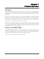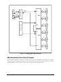
1
CORELIS SCANIO-280LV SCANIO -280LV Boundary-Scan Based Digital Tester User’s Manual CORELIS SCANIO-280LV SCANIO -280LV Boundary-Scan Based Digital Tester User’s Manual Copyright 1999-2002 Corelis Inc. 12607 Hiddencreek Way Cerritos, CA 90703-2146 Telephone: (562) 926-6727 • Fax: (562) 404-6196 i Preface PRINTING HISTORY New editions are complete revisions of the manual. Update packages, which are issued between editions, contain additional and replacement pages to be merged into the manual by the customer. The dates on the title page change only when a new edition is published. A software code may be printed before the date; this indicates the version of the software product at the time the manual or update was issued. Many product updates and fixes do not require manual changes and, conversely, manual corrections may be done without accompanying product changes. Therefore, do not expect a one to one correspondence between product updates and manual updates. Edition 1, July 1999 Edition 2, November 2001 Edition 3, June 2002 GENERAL NOTICE Information contained in this document is subject to change without notice. CORELIS shall not be liable for errors contained herein for incidental or consequential damages in connection with the furnishing, performance, or use of material contained in this manual. This document contains proprietary information, which is protected by copyright. All rights reserved. No part of this document may be reproduced or translated to other languages without the prior written consent of CORELIS. CORELIS assumes no responsibility for the use of or reliability of its software on equipment that is not furnished by CORELIS. ii PRODUCT WARRANTY This CORELIS product has a warranty against defects in material and workmanship for a period of 90 days from date of shipment. During the warranty period, CORELIS will, at its option, either repair or replace products that prove to be defective. For warranty service or repair, this product must be returned to a service facility designated by CORELIS. Outside CORELIS service travel areas, warranty service will be performed at the Buyer's facility only upon CORELIS' prior agreement and Buyer shall pay CORELIS' round trip travel expenses. For products returned to CORELIS for warranty service, the Buyer shall prepay shipping charges to CORELIS and CORELIS shall pay shipping charges to return the product to the Buyer. However, the Buyer shall pay all shipping charges, duties, and taxes for products returned to CORELIS from another country. CORELIS warrants that its software and firmware designated by CORELIS for use with an instrument will execute its programming instructions when properly installed on that instrument. CORELIS does not warrant that the operation of the instrument, software, or firmware will be uninterrupted or error-free. The foregoing warranty shall not apply to defects resulting from improper or inadequate maintenance by the Buyer, Buyer-supplied software or interfacing, unauthorized modification or misuse, operation outside of the environmental specifications for the product, or improper site preparation or maintenance. NO OTHER WARRANTY IS EXPRESSED OR IMPLIED. CORELIS SPECIFICALLY DISCLAIMS THE IMPLIED WARRANTIES OF MERCHANTABILITY AND FITNESS FOR A PARTICULAR PURPOSE. EXCLUSIVE REMEDIES THE REMEDIES CONTAINED HEREIN ARE THE CUSTOMER'S SOLE AND EXCLUSIVE REMEDIES. CORELIS SHALL NOT BE LIABLE FOR ANY DIRECT, INDIRECT, SPECIAL, INCIDENTAL, OR CONSEQUENTIAL DAMAGES, WHETHER BASED ON CONTRACT, TORT, OR ANY OTHER LEGAL THEORY. Product maintenance agreements and other customer assistance agreements are available for Corelis products. For assistance, contact your nearest Corelis Sales and Service Office. RETURN POLICY No items returned to CORELIS for warranty, service, or any other reason shall be accepted unless first authorized by CORELIS, either direct or through its authorized sales representatives. All returned items must be shipped pre-paid and clearly display a Returned Merchandise Authorization (RMA) number on the shipping carton. Freight collect items will NOT be accepted. Customers or authorized sales representatives must first contact CORELIS with notice of request for return of merchandise. RMA's can only originate from CORELIS. If authorization is granted, an RMA number will be forwarded to the customer either directly or through its authorized sales representative. iii Table Of Contents CHAPTER 1 PRODUCT OVERVIEW ..........................................................................1-1 Introduction..............................................................................................................................................................1-1 Features of the SCANIO -280LV..........................................................................................................................1-1 288 Individually Controlled I/O Signals ................................................................................................................ 1-2 Adjustable Voltage Interfaces ................................................................................................................................ 1-3 Daisy Chaining the TAPs....................................................................................................................................... 1-3 SCANIO -280LV Specifications............................................................................................................................1-3 CHAPTER 2 SCANIO -280LV INSTALLATION.........................................................2-1 Introduction..............................................................................................................................................................2-1 Setting the Interface Voltage...................................................................................................................................2-2 Connecting to the JTAG Controller .......................................................................................................................2-2 Target TAP Connection...........................................................................................................................................2-3 Target TAP Design ..................................................................................................................................................2-4 Target TAP Schematics ...........................................................................................................................................2-5 Daisy Chaining the SCANIO -280LV...................................................................................................................2-5 Digital I/O Test Connection ....................................................................................................................................2-7 Mating Connectors.................................................................................................................................................2-14 CHAPTER 3 PROVIDED SOFTWARE ........................................................................3-1 What’s on the Disk...................................................................................................................................................3-1 Executing Selftest with ScanPlus Runner ..............................................................................................................3-2 Infrastructure Test .................................................................................................................................................. 3-2 Interconnect and Buswire Tests ............................................................................................................................. 3-4 Using the SCANIO -280LV Files ..........................................................................................................................3-5 Boundary-Scan Topology ...................................................................................................................................... 3-5 Boundary-Scan Description Language (BSDL)..................................................................................................... 3-5 Netlist Edit File ...................................................................................................................................................... 3-6 Netlist..................................................................................................................................................................... 3-6 CHAPTER 4 APPLICATION EXAMPLE WITH SCANPLUS TPG...............................4-1 Introduction..............................................................................................................................................................4-1 Description of the Unit Under Test.........................................................................................................................4-2 iv TAP Connection and Termination ......................................................................................................................... 4-2 SCANIO-280LV Interface.................................................................................................................................. 4-2 Generating Test Vectors with ScanPlus TPG........................................................................................................4-2 Example Topology File.......................................................................................................................................... 4-3 Using the Netlist Edit File...................................................................................................................................... 4-4 Creating Test Vectors............................................................................................................................................. 4-5 v Table of Figures Figure 1-1. Figure 2-1. Figure 2-2. Figure 2-3. Figure 2-4. Figure 2-5. Figure 2-6. Figure 3-1. Figure 3-2. Figure 3-3. Figure 3-4. Figure 4-1. Figure 4-2. Figure 4-3. Figure 4-4. SCANIO-280LV Block Diagram .........................................................................................................1-2 Connections Between JTAG Controller, SCANIO-280LV, and UUT ....................................................2-2 TAP Connection Between SCANIO-280LV and UUT.........................................................................2-4 Standard TAP connector (top view).......................................................................................................2-4 TAP Connector Schematics....................................................................................................................2-5 TAP Connection for Two Daisy Chained SCANIO-280LVs and a UUT................................................2-6 60-pin Connector Pin Numbering..........................................................................................................2-7 ScanPlus Runner Infrastructure Test .....................................................................................................3-3 ScanPlus Runner Interconnect and Buswire Test ..................................................................................3-4 Topology File Scanio.top .......................................................................................................................3-5 Netlist Edit File Scanio.edt ....................................................................................................................3-6 Schematic of an Example Unit Under Test ............................................................................................4-1 Example Topology File ..........................................................................................................................4-4 Netlist Edit File for Example Design .....................................................................................................4-5 ScanPlus TPG Test Step.........................................................................................................................4-6 vi Table of Tables Table 2-1. TAP In Connection List ...........................................................................................................................2-3 Table 2-2. TAP Out Connection List.........................................................................................................................2-3 Table 2-3. J1 Connector Pin Assignment..................................................................................................................2-8 Table 2-4. J2 Connector Pin Assignment..................................................................................................................2-9 Table 2-5. J3 Connector Pin Assignment................................................................................................................2-10 Table 2-6. J4 Connector Pin Assignment................................................................................................................2-11 Table 2-7. J5 Connector Pin Assignment................................................................................................................2-12 Table 2-8. J6 Connector Pin Assignment................................................................................................................2-13 Table 2-9. Mating Connectors for the SCANIO-280LV.......................................................................................2-14 Table 2-10. Mating TAP Connector for PCI-1149.1 and PC-1149.1/100F............................................................2-14 vii Chapter 1 Product Overview Introduction The SCANIO™-280LV Digital Tester module provides a low cost alternative to traditional stimulus response digital testing. Through the use of boundary-scan technology, the SCANIO™-280LV module provides a total of 288 fully bidirectional test channels with virtually unlimited memory depth per pin. The module uses boundary-scan gate arrays to add control and visibility to connectors, traces, and logic that are otherwise untestable using boundary-scan techniques. The SCANIO™-280, combined with a boundary-scan controller such as the Corelis PCI-1149.1, PC-1149.1/100F, or Net1149.1, operates as a traditional "bed of nails" test system except access to the stimulus-andresponse I/Os is accomplished using boundary-scan technology. Each pin can be individually configured as an input, output, or tri-state. Blocks of 144 I/O channels can be bypassed (using the boundary-scan bypass command), thus reducing the number of channels to fit the number of UUT I/O's. Reducing the number of I/O channels reduces test times which can be important in time-critical test applications. Features of the SCANIO-280LV The SCANIO-280LV is built around two fully boundary-scan compliant chips and supports 288 individually controllable digital I/O. The TAP and digital I/O are 5V tolerant and their interface voltage can be configured to interface with 2.5V, 3.3V or 5.0V systems. The SCANIO-280LV can be daisy chained on a single TAP to other SCANIO-280LVs or targets. Figure 1-1 shows a block diagram of the SCANIO-280LV. Product Overview 1-1 48 TAP IN TDO TDI TDO TDI TDO B U F F E R TDI TDI J1 ASIC1 48 J3 TAP OUT 48 V O L T A G E A D J U S T J5 TDO 48 TDI J2 ASIC2 48 J4 48 TDO J6 Figure 1-1. SCANIO -280LV Block Diagram 288 Individually Controlled I/O Signals The SCANIO-280LV contains two ASICS each with 144 individually controlled I/O signals. Each I/O has a boundary-scan input cell, output cell and control cell associated with it. Each pin can individually be set to read only, write only or read and write simultaneously. Product Overview 1-2 Adjustable Voltage Interfaces The voltage level of the I/O and TAP interfaces is controlled by the adjust rotary switch and can be set to any voltage between 2.0V and 3.4V in increments of 0.10V. The SCANIO-280LV has been characterized at 2.5V and 3.3V and has not been tested at the other voltage levels. The I/O and TAP interfaces are 5V tolerant at all voltage levels. Daisy Chaining the TAPs The TAP In and a TAP Out connectors are used to daisy chain the TAPs of one or more boards. Typically, the SCANIO-280LV is connected in series with the boundary-scan target. The SCANIO-280LV also can be used in stand-alone mode, or several SCANIO-280LVs can be daisy chained together along with a target. SCANIO-280LV Specifications Size and Form Factor Dimensions 9.580” x 7.453” x 0.792” Number of Test Points 288 per module, expandable to more lines by connecting multiple modules in series Test Point Configurations Supported Each test point is individually programmable as input, output or bidirectional Bypass Capability Either of the two blocks of 144 points may be bypassed on the ASICs. Maximum ASIC Test Clock (TCK) Frequency Maximum TCK Frequency Product Overview 10MHz 1-3 I/O and TAP Signals DC Characteristics Symbol Parameter Conditions MIN MAX UNIT VCC Adjustable Voltage 3.3V and 5V interfaces 3.0 3.4 V VCC Adjustable Voltage 2.5V interface 2.3 2.7 V VIH High Level Input Voltage 1.7 5.75 V VIL Low Level Input Voltage -0.5 0.8 V VOH 3.0V VCC 2.3V VCC VOL 3.0V VCC 2.3V VCC IOH=-8mA DC 2.4 V IOH=-0.1mA DC VCC-0.2 V IOH=-100µA DC 2.1 V IOH=-1mA DC 2.0 V IOH=-2mA DC 1.7 V IOL=8mA DC 0.45 V IOL= 0.1mA DC 0.2 V IOL= 100µA DC 0.2 V IOL= 1mA DC 0.4 V IOL= 2mA DC 0.7 V II Input leakage current VI = VCC or ground -10 10 µA IOZ Tri-state output off-state current VO = VCC or ground -10 10 µA Note: It is recommended that no more than 50% of the outputs on any of the following two I/O groups be subjected to the maximum current limits specified above at any one time: Group1: J1, J3, J5 Group2: J2, J4, J6 Product Overview 1-4 I/O Connectors JTAG Connector (TAP In) JTAG Connector (TAP Out) I/O Connectors (J1-J6) 10-pin IDC (3M part no. 3793-6302 or equivalent) 10-pin IDC (3M part no. 3793-6302 or equivalent) 60-pin IDC (3M part no. 3372-6302 or equivalent) Power Requirements (From External Power Supply) 5 Volts 3.0 Amp (Maximum) Operating Environment Temperature 0°C to 55°C Relative Humidity 10% to 90%, non condensing Storage Environment Temperature Product Overview -40°C to 85°C 1-5 Chapter 2 SCANIO SCANIO-280LV Installation The SCANIO-280LV product consists of the following components: • • • • SCANIO-280LV Hardware 5V External Power Supply SCANIO-280LV Software Disk SCANIO-280LV User’s Manual Ensure all materials listed are present and free from visible damage or defects before proceeding. If anything appears to be missing or damaged, contact Corelis at the number listed on the front cover immediately. Introduction To ensure reliable operation of the SCANIO-280LV, it is important that it is connected properly to both the boundary-scan tester and the unit to be tested. If the design incorporates the recommended connectors and pin assignments then all connections are made with simple 1:1 cables. Figure 2-1 shows the cable connections between the JTAG controller, the SCANIO-280LV, and the target UUT. SCANIO-280LV Installation 2-1 Corelis PCI-1149.1 or PC-1148.1/100F Boundary-Scan Controller 40-Pin to 10-Pin 1:1 SCANIO-280LV TAP In TAP Out J1 J2 J3 J4 J5 J6 60-Pin 1:1 Cable 10-Pin 1:1 Cable I/O Connector TAP TARGET Figure 2-1. Connections Between JTAG Controller, SCANIO-280LV, and UUT Setting the Interface Voltage Before connecting to the boundary-scan controller or the target Unit Under Test (UUT) it is necessary to set the interface voltage. The Adjust rotary switch sets the interface voltage of the TAP and I/O pins to voltages between 2.0V and 3.4V. Use a small screwdriver to set the interface voltage. The voltage appears on the LEDs. The SCANIO-280LV retains the set voltage interface value when powered on and off, however, it is better to check the interface voltage (by viewing the LEDs) before connecting to a target board, as an incorrect voltage setting may damage some targets. Connecting to the JTAG Controller The SCANIO-280LV is connected to the JTAG controller via connector TAP In. Table 2-1 shows the pin assignment for the TAP In connector. The TAP In connector is the Corelis standard connector and can be connected to the Corelis controllers PCI-1149.1 or PC-1149.1/100F using a 40-pin to 10-pin 1:1 cable, and can be connected to the other Corelis controllers with the cable provided with them. SCANIO-280LV Installation 2-2 Pin 1 2 3 4 5 6 7 8 9 10 Signal Name TRST* GND TDI GND TDO GND TMS GND TCK GND I/O In In Out In In Description TRST* Ground Test Data In Ground Test Data Out Ground Test Mode Select Ground Test Clock Ground Table 2-1. TAP In Connection List Target TAP Connection Connect the target TAP to the TAP Out connector of the SCANIO-280LV. The TAP Out connector has presence detect logic that will detect the UUT board and will include the UUT in the scan chain. Figure 2-2 shows a diagram of this configuration. If the target system has no boundary-scan logic and no TAP, do not connect anything to TAP Out. Table 2-2 shows the connection list for the TAP Out connector. Pin 1 2 3 4 5 6 7 8 9 10 Signal Name TRST_TO_UUT GND TDO_TO_UUT GND TDI_FROM_UUT GND TMS_TO_UUT GND TCK_TO_UUT GND I/O Out Out In Out Out Description Test Reset to UUT scan chain Ground Test Data Out to UUT scan chain Ground Test Data In from UUT scan chain Ground Test Mode Select to UUT scan chain Ground Test Clock to UUT scan chain Ground Table 2-2. TAP Out Connection List SCANIO-280LV Installation 2-3 SCANIO™-280LV TAP PCI-1149.1, PC-1149.1/100F, PCMCIA, NET-1149.1 Boundary-Scan Controllers or ANY IEEE-1149.1 Compliant Controller TAP In TAP Out TDI TDO ASIC1 TDO TDI ASIC2 I/Os TAP UNIT UNDER TEST Figure 2-2. TAP Connection Between SCANIO -280LV and UUT Target TAP Design The TAP contains 5 signals: TCK, TMS, TDO, TDI and optionally TRST*. It also contains ground signal(s). The Corelis recommended standard TAP connector is shown in Figure 2-3 and is widely regarded as the industry standard. Note that each signal is terminated with resistor in order to minimize signal cross-talk in the interface cable and maximize noise immunity. The connector on the user’s target should have the standard flat cable compatible pinout. Below is the top view of the target 10-pin connector header (0.100" x 0.100" spacing): TRST* 1 2 GND TDI 3 4 GND TDO 5 6 GND TMS 7 8 GND TCK 9 10 GND Figure 2-3. Standard TAP connector (top view) SCANIO-280LV Installation 2-4 The following are two 3M brand part numbers for the above connector. Both are 0.100" x 0.100" headers, one with and one without latch/ejector. Note that there are many other manufacturers who would have similar parts as well: 3M Part Number Description 30310-6002HB Straight header, 10 pin, 4 wall, with center notch 3793-5602UG Latch/Ejector Straight header, 10 pin, 4 wall, with notch Target TAP Schematics The typical schematics of the target TAP connector and the recommended termination resistors are shown in Figure 2-4. The 1K pull-up resistors can be connected to any Vcc supply with nominal voltage between 2.5V to 5.0V. Recommended resistor values are +/- 5%. Vcc Vcc Vcc Vcc Target Board 1K 1K 1K 1K TRST* To all Boundary Scan Devices TDI To TDI of 1st Device in the chain 33 From TDO of last Devices in chain TDO TMS To all Boundary Scan Devices TCK To all Boundary Scan Devices 1 2 3 4 5 6 7 8 9 10 TAP Connector Figure 2-4. TAP Connector Schematics Daisy Chaining the SCANIO-280LV The TAP Out port can be used to daisy chain multiple SCANIO-280LV modules together to form a high pin count digital test system. A straight ten contact socket connector to socket connector flat cable can be used to connect adjacent SCANIO-280LV modules. Connect the TAP Out from the first SCANIO-280LV module to the TAP In on the second module. Repeat this until all modules are daisy chained. Connect the UUT to the TAP Out of the last SCANIO280LV. Figure 2-5 show the TAP connections for two daisy chained SCANIO-280LV modules and a target UUT. SCANIO-280LV Installation 2-5 Corelis PCI-1149.1 or PC-1148.1/100F Boundary-Scan Controller 40-Pin to 10-Pin 1:1 SCANIO-280LV TAP In TAP Out J1 J2 J3 J4 J5 J6 10-Pin 1:1 Cable SCANIO-280LV TAP Out TAP In J1 J2 J3 J4 J5 J6 10-Pin 1:1 Cable I/O Connector TAP TARGET Figure 2-5. TAP Connection for Two Daisy Chained SCANIO-280LVs and a UUT SCANIO-280LV Installation 2-6 Digital I/O Test Connection Each SCANIO-280LV contains six 60-pin connectors which provide the digital I/O channels used for testing. Each of these 280 channels can be independently programmed as input, output or tri-state (high impedance). To create a test system, these test connectors need to be connected to the unit under test using a set of ribbon cables. Figure 2-6 shows the way that the connectors are numbered. To assist in the building of these cables Table 2-3 through Table 2-8 show the pin assignments for connectors J1 to J6. PIN 2 PIN 1 PIN 4 PIN 3 Figure 2-6. 60-pin Connector Pin Numbering SCANIO-280LV Installation 2-7 PIN Signal ASIC.Pin PIN Signal ASIC.Pin 1 J1_1 ASIC1.101 2 J1_2 ASIC1.102 3 5 J1_3 GND ASIC1.108 4 6 J1_4 J1_6 ASIC1.109 ASIC1.110 7 9 J1_7 J1_9 ASIC1.111 ASIC1.113 8 10 J1_8 GND ASIC1.112 11 J1_11 ASIC1.114 12 J1_12 ASIC1.115 13 15 J1_13 GND ASIC1.117 14 16 J1_14 J1_16 ASIC1.118 ASIC1.119 17 J1_17 ASIC1.120 18 J1_18 ASIC1.121 19 21 23 J1_19 J1_21 J1_23 ASIC1.122 ASIC1.123 ASIC1.126 20 22 24 GND J1_22 J1_24 ASIC1.124 ASIC1.128 25 27 GND J1_27 ASIC1.130 26 28 J1_26 J1_28 ASIC1.129 ASIC1.131 29 31 J1_29 J1_31 ASIC1.132 ASIC1.133 30 32 GND J1_32 ASIC1.135 33 35 J1_33 GND ASIC1.136 34 36 J1_34 J1_36 ASIC1.137 ASIC1.138 37 39 J1_37 J1_39 ASIC1.139 ASIC1.141 38 40 J1_38 GND ASIC1.140 41 43 J1_41 J1_43 ASIC1.142 ASIC1.145 42 44 J1_42 J1_44 ASIC1.144 ASIC1.146 45 47 49 51 53 55 GND J1_47 J1_49 J1_51 J1_53 GND ASIC1.148 ASIC1.150 ASIC1.151 ASIC1.154 46 48 50 52 54 56 J1_46 J1_48 GND J1_52 J1_54 J1_56 ASIC1.147 ASIC1.149 57 59 J1_57 J1_59 ASIC1.161 ASIC1.163 58 60 J1_58 GND ASIC1.162 ASIC1.153 ASIC1.159 ASIC1.160 Table 2-3. J1 Connector Pin Assignment SCANIO-280LV Installation 2-8 PIN Signal 1 J2_1 3 J2_3 5 7 ASIC.Pin PIN Signal ASIC2.101 2 J2_2 ASIC2.102 ASIC2.108 4 J2_4 ASIC2.109 GND J2_7 ASIC2.111 6 8 J2_6 J2_8 ASIC2.110 ASIC2.112 9 J2_9 ASIC2.113 10 GND 11 13 J2_11 J2_13 ASIC2.114 ASIC2.117 12 14 J2_12 J2_14 ASIC2.115 ASIC2.118 15 GND 16 J2_16 ASIC2.119 17 J2_17 ASIC2.120 18 J2_18 ASIC2.121 19 21 J2_19 J2_21 ASIC2.122 ASIC2.123 20 22 GND J2_22 ASIC2.124 23 25 J2_23 GND ASIC2.126 24 26 J2_24 J2_26 ASIC2.128 ASIC2.129 27 29 J2_27 J2_29 ASIC2.130 ASIC2.132 28 30 J2_28 GND ASIC2.131 31 33 J2_31 J2_33 ASIC2.133 ASIC2.136 32 34 J2_32 J2_34 ASIC2.135 ASIC2.137 35 37 GND J2_37 ASIC2.139 36 38 J2_36 J2_38 ASIC2.138 ASIC2.140 39 41 J2_39 J2_41 ASIC2.141 ASIC2.142 40 42 GND J2_42 ASIC2.144 43 45 47 J2_43 GND J2_47 ASIC2.145 44 46 48 J2_44 J2_46 J2_48 ASIC2.146 ASIC2.147 ASIC2.149 49 51 53 55 57 J2_49 J2_51 J2_53 GND J2_57 ASIC2.150 ASIC2.151 ASIC2.154 ASIC2.161 50 52 54 56 58 GND J2_52 J2_54 J2_56 J2_58 ASIC2.153 ASIC2.159 ASIC2.160 ASIC2.162 59 J2_59 ASIC2.163 60 GND ASIC2.148 ASIC.Pin Table 2-4. J2 Connector Pin Assignment SCANIO-280LV Installation 2-9 PIN Signal 1 3 J3_1 J3_3 5 7 ASIC.Pin PIN Signal ASIC1.39 ASIC1.42 2 4 J3_2 J3_4 ASIC1.40 ASIC1.43 GND J3_7 ASIC1.45 6 8 J3_6 J3_8 ASIC1.44 ASIC1.46 9 J3_9 ASIC1.47 10 GND 11 J3_11 ASIC1.48 12 J3_12 ASIC1.49 13 15 J3_13 GND ASIC1.55 14 16 J3_14 J3_16 ASIC1.56 ASIC1.57 17 J3_17 ASIC1.58 18 J3_18 ASIC1.58 19 21 J3_19 J3_21 ASIC1.60 ASIC1.61 20 22 GND J3_22 ASIC1.62 23 25 J3_23 GND ASIC1.64 24 26 J3_24 J3_26 ASIC1.65 ASIC1.66 27 29 J3_27 J3_29 ASIC1.67 ASIC1.69 28 30 J3_28 GND ASIC1.68 31 33 J3_31 J3_33 ASIC1.70 ASIC1.73 32 34 J3_32 J3_34 ASIC1.71 ASIC1.76 35 37 GND J3_37 ASIC1.78 36 38 J3_36 J3_38 ASIC1.77 ASIC1.79 39 41 J3_39 J3_41 ASIC1.80 ASIC1.81 40 42 GND J3_42 ASIC1.84 43 45 47 J3_43 GND J3_47 ASIC1.86 44 46 48 J3_44 J3_46 J3_48 ASIC1.67 ASIC1.88 ASIC1.90 49 51 53 55 57 59 J3_49 J3_51 J3_53 GND J3_57 J3_59 ASIC1.91 ASIC1.92 ASIC1.95 50 52 54 56 58 60 GND J3_52 J3_54 J3_56 J3_58 GND ASIC1.93 ASIC1.96 ASIC1.97 ASIC1.99 ASIC1.89 ASIC1.98 ASIC1.100 ASIC.Pin Table 2-5. J3 Connector Pin Assignment SCANIO-280LV Installation 2-10 PIN Signal 1 3 J4_1 J4_3 5 7 ASIC.Pin PIN Signal ASIC2.39 ASIC2.42 2 4 J4_2 J4_4 ASIC2.40 ASIC2.43 GND J4_7 ASIC2.45 6 8 J4_6 J4_8 ASIC2.44 ASIC2.46 9 J4_9 ASIC2.47 10 GND 11 J4_11 ASIC2.48 12 J4_12 ASIC2.49 13 15 J4_13 GND ASIC2.55 14 16 J4_14 J4_16 ASIC2.56 ASIC2.57 17 J4_17 ASIC2.58 18 J4_18 ASIC2.58 19 21 J4_19 J4_21 ASIC2.60 ASIC2.61 20 22 GND J4_22 ASIC2.62 23 25 J4_23 GND ASIC2.64 24 26 J4_24 J4_26 ASIC2.65 ASIC2.66 27 29 J4_27 J4_29 ASIC2.67 ASIC2.69 28 30 J4_28 GND ASIC2.68 31 33 J4_31 J4_33 ASIC2.70 ASIC2.73 32 34 J4_32 J4_34 ASIC2.71 ASIC2.76 35 37 GND J4_37 ASIC2.78 36 38 J4_36 J4_38 ASIC2.77 ASIC2.79 39 41 J4_39 J4_41 ASIC2.80 ASIC2.81 40 42 GND J4_42 ASIC2.84 43 45 47 J4_43 GND J4_47 ASIC2.86 44 46 48 J4_44 J4_46 J4_48 ASIC2.67 ASIC2.88 ASIC2.90 49 51 53 55 57 59 J4_49 J4_51 J4_53 GND J4_57 J4_59 ASIC2.91 ASIC2.92 ASIC2.95 50 52 54 56 58 60 GND J4_52 J4_54 J4_56 J4_58 GND ASIC2.93 ASIC2.96 ASIC2.97 ASIC2.99 ASIC2.89 ASIC2.98 ASIC2.100 ASIC.Pin Table 2-6. J4 Connector Pin Assignment SCANIO-280LV Installation 2-11 PIN Signal ASIC.Pin PIN Signal 1 3 5 J5_1 J5_3 GND 7 ASIC1.187 ASIC1.190 2 4 6 J5_2 J5_4 J5_6 ASIC1.188 ASIC1.192 ASIC1.193 J5_7 ASIC1.194 8 J5_8 ASIC1.195 9 J5_9 ASIC1.196 10 GND 11 13 J5_11 J5_13 ASIC1.197 ASIC1.199 12 14 J5_12 J5_14 ASIC1.198 ASIC1.201 15 17 GND J5_17 ASIC1.203 16 18 J5_16 J5_18 ASIC1.202 ASIC1.204 19 21 J5_19 J5_21 ASIC1.205 ASIC1.206 20 22 GND J5_22 ASIC1.3 23 J5_23 ASIC1.4 24 J5_24 ASIC1.6 25 27 GND J5_27 ASIC1.8 26 28 J5_26 J5_28 ASIC1.7 ASIC1.9 29 31 J5_29 J5_31 ASIC1.10 ASIC1.11 30 32 GND J5_32 ASIC1.12 33 35 J5_33 GND ASIC1.13 34 36 J5_34 J5_36 ASIC1.15 ASIC1.16 37 39 41 43 45 47 49 51 53 55 57 59 J5_37 J5_39 J5_41 J5_43 GND J5_47 J5_49 J5_51 J5_53 GND J5_57 J5_59 ASIC1.17 ASIC1.19 ASIC1.20 ASIC1.22 38 40 42 44 46 48 50 52 54 56 58 60 J5_38 GND J5_42 J5_44 J5_46 J5_48 GND J5_52 J5_54 J5_56 J5_58 GND ASIC1.18 ASIC1.26 ASIC1.28 ASIC1.29 ASIC1.33 ASIC1.36 ASIC1.38 ASIC.Pin ASIC1.21 ASIC1.24 ASIC1.25 ASIC1.27 ASIC1.31 ASIC1.34 ASIC1.35 ASIC1.37 Table 2-7. J5 Connector Pin Assignment SCANIO-280LV Installation 2-12 PIN Signal ASIC.Pin PIN Signal 1 3 5 J6_1 J6_3 GND 7 ASIC2.187 ASIC2.190 2 4 6 J6_2 J6_4 J6_6 ASIC2.188 ASIC2.192 ASIC2.193 J6_7 ASIC2.194 8 J6_8 ASIC2.195 9 J6_9 ASIC2.196 10 GND 11 13 J6_11 J6_13 ASIC2.197 ASIC2.199 12 14 J6_12 J6_14 ASIC2.198 ASIC2.201 15 17 GND J6_17 ASIC2.203 16 18 J6_16 J6_18 ASIC2.202 ASIC2.204 19 21 J6_19 J6_21 ASIC2.205 ASIC2.206 20 22 GND J6_22 ASIC2.3 23 J6_23 ASIC2.4 24 J6_24 ASIC2.6 25 27 GND J6_27 ASIC2.8 26 28 J6_26 J6_28 ASIC2.7 ASIC2.9 29 31 J6_29 J6_31 ASIC2.10 ASIC2.11 30 32 GND J6_32 ASIC2.12 33 35 J6_33 GND ASIC2.13 34 36 J6_34 J6_36 ASIC2.15 ASIC2.16 37 39 41 43 45 47 49 51 53 55 57 59 J6_37 J6_39 J6_41 J6_43 GND J6_47 J6_49 J6_51 J6_53 GND J6_57 J6_59 ASIC2.17 ASIC2.19 ASIC2.20 ASIC2.22 38 40 42 44 46 48 50 52 54 56 58 60 J6_38 GND J6_42 J6_44 J6_46 J6_48 GND J6_52 J6_54 J6_56 J6_58 GND ASIC2.18 ASIC2.26 ASIC2.28 ASIC2.29 ASIC2.33 ASIC2.36 ASIC2.38 ASIC.Pin ASIC2.21 ASIC2.24 ASIC2.25 ASIC2.27 ASIC2.31 ASIC2.34 ASIC2.35 ASIC2.37 Table 2-8. J6 Connector Pin Assignment SCANIO-280LV Installation 2-13 Mating Connectors Table 2-9 shows the mating connectors needed to make cables for the JTAG connector and the I/O port connectors. Table 2-10 shows the mating 40-pin TAP connector for the PCI-1149.1 and the PC-1149.1/100F. Reference Description TAP In, TAP Out J1-J6 Manufacturer Part Number 10 pin .100 x .100 Wiremount Socket 3M 3473-6610 Strain Relief 3M 3M 3448-3010 3334-6660 3M 3448-3060 60 pin .100 x .100 Wiremount Socket Strain Relief Table 2-9. Mating Connectors for the SCANIO -280LV Reference Description P1 40 pin .100 x .100 Wiremount Socket Strain Relief Manufacturer Part Number 3M 3417-6640 3M 3448-3040 Table 2-10. Mating TAP Connector for PCI-1149.1 and PC-1149.1/100F SCANIO-280LV Installation 2-14 Chapter 3 Provided Software What’s on the Disk The disk contains the following files: Filename ASIC280LV.bsd Scanio.edt Scanio.net Scanio.top \Example\74bct8374 \Example\ASIC280LV.bsd \Example\JDB.net \Example\Scanio&JDB.edt Description BSDL file for the SCANIO-280LV boundary-scan components. Netlist edit file for use with Corelis ScanPlus tools. Partial netlist shows connection of the digital I/Os of the two boundary-scan components. Boundary-scan topology file for use with Corelis ScanPlus tools. Shows the scan chain from TDI to TDO of the SCANIO-280LV. BSDL file for SN74BCT8374 boundary-scan chips on example Unit Under Test. BSDL file for the SCANIO-280LV boundary-scan components. Telesis format netlist of example UUT. Netlist edit file for example UUT and SCANIO-280LV. \Example\STD_1149_1_1990 Topology file showing scan chain for example UUT and SCANIO-280LV. 1990 IEEE 1149.1 VHDL Package \Example\STD_1149_1_1994 1994 IEEE 1149.1 VHDL Package \Selftest\ASIC280LV.bsd BSDL file for the SCANIO-280LV boundary-scan components. \Example\Scanio&JDB.top \Selftest\Scanio.top \Selftest\Scanio.net Boundary-scan topology file for use with Corelis ScanPlus tools. Shows the scan chain from TDI to TDO of the SCANIO-280LV. Partial netlist shows connection of the digital I/Os of the two boundary-scan components. \Selftest\ScanioLoopBack.edt Netlist edit file that merges connectors J1 with J2, J3 with J4 and J5 with J6 for use with ScanPlus TPG for loopback test pattern generation. \Selftest\Selftest_Buswire_bus.cvf Selftest buswire test vector file. Requires Corelis ScanPlus Runner to execute test. Must connect 60 pin 1:1 cables from J1 to J2, from J3 to J4, and from J5 to J6. \Selftest\Selftest_Interconnect_int.cvf Selftest interconnect test vector file. Requires Corelis ScanPlus Runner to execute test. Must connect 60 pin Provided Software 3-1 Filename Description 1:1 cables from J1 to J2, from J3 to J4, and from J5 to J6. \Selftest\Selftest_Infrastructure_inf.cvf \Selftest\STD_1149_1_1994 Selftest infrastructure test vector file. Requires Corelis ScanPlus Runner to execute test. 1994 IEEE 1149.1 VHDL Package Executing Selftest with ScanPlus Runner The SCANIO-280LV comes with three (3) compact vector format selftest files, Selftest_Infrastructure_inf.cvf, Selftest_Interconnect_ic.cvf Selftest_Buswire_bus.cvf . In order to execute these files you need Corelis ScanPlus Runner test execution software and a Corelis Boundary-Scan controller such as the PC-1149.1/100F or PCI-1149.1 with cable. To complete all three tests three (3) sixty pin 1:1 cables are necessary to provide loopback on the digital I/O signals. Infrastructure Test The infrastructure test verifies that a good TAP connection is being made between the controller and the SCANIO-280LV. It also verifies that the boundary-scan infrastructure of the two ASICs on the SCANIO-280LV is fully functional. The infrastructure test requires a Corelis boundaryscan controller, a SCANIO-280LV unit and a cable to connect the two. Please follow these steps: STEP1. STEP2. STEP3. STEP4. STEP5. STEP6. STEP7. STEP8. STEP9. STEP10. Connect the 5V power supply to the SCANIO-280LV. Make sure no target is connected to the SCANIO-280LV, then power it up by turning on the Power Switch. Set the interface voltage by using a screwdriver to rotate the adjust switch. All three selftests can be run at any voltage. Connect one end of the TAP cable to the boundary-scan controller and the other end to TAP In connector on the SCANIO-280LV. Double click on the ScanPlus Runner Icon. Select File:New Test Plan. Click on the Add button and add Selftest_Infrastructure_inf.cvf. Select OK. Select Set-up:Controller then select the boundary-scan controller being used and set the frequency to 10MHz. Select Run Test. The test should run and pass. Figure 3-1 shows a passing infrastructure test. Provided Software 3-2 Figure 3-1. ScanPlus Runner Infrastructure Test Provided Software 3-3 Interconnect and Buswire Tests The interconnect and buswire tests verify that all 288 digital I/Os of the SCANIO-280LV are fully functional. These tests are completed without a target attached. To test all of the I/Os, three (3) 60-pin 1:1 cables must be connected between pairs J1 and J2, J3 and J4, and J5 and J6 to establish interconnectivity between the connectors. Note that this test not only tests the SCANIO-280LV digital I/Os but also tests the connectivity of the 60-pin 1:1 cables. If you are using 60-pin 1:1 cables to connect to your target, this is a good way to verify that the cables are good. The interconnect and buswire tests will be run in a single test plan that includes the infrastructure test. Please follow these steps: STEP1. STEP2. STEP3. STEP4. STEP5. STEP6. STEP7. STEP8. STEP9. STEP10. STEP11. Connect the 5V power supply to the SCANIO-280LV. Make sure no target is connected to the SCANIO-280LV, then power it up by turning on the Power Switch. Set the interface voltage by using a screwdriver to rotate the adjust switch. All three selftests can be run at any voltage. Connect one end the TAP cable to the boundary-scan controller and the other end to TAP In Connector on the SCANIO-280LV. Connect a 60-pin 1:1 cable between J1 and J2. Connect a 60-pin 1:1 cable between J3 and J4. Connect a 60-pin 1:1 cable between J5 and J6. Double click on the ScanPlus Runner Icon. Select File:New Test Plan. Click on the Add button and add Selftest_Infrastructure_inf.cvf, Selftest_Interconnect_ic, and Selftest_Buswire_bus.cvf in that order. Select OK. Select Set-up:Controller then select the boundary-scan controller being used and set the frequency to 10MHz. Select Run Test. The test should run and pass. Figure 3-2 shows the results of running these tests. Figure 3-2. ScanPlus Runner Interconnect and Buswire Test Provided Software 3-4 Using the SCANIO-280LV Files The SCANIO-280LV has four files that describe its functionality: Scanio.top, Scanio.net, Scanio.edt, and Scanio.bsd. These files can also be used as inputs to the Corelis ScanPlus software. Boundary-Scan Topology The scan chain for the SCANIO-280LV is described in the topology file Scanio.top shown in Figure 3-3 below. The file shows that the SCANIO-280LV contains two boundary-scan devices in order from TDI to TDO that are referenced as ASIC1 and ASIC2. These two devices are described by BSDL file ASIC280LV.BSD and they are 208 pin PQFP devices. When a second boundary-scan UUT is connected to the SCANIO-280LV via the TAP Out connector, it follows the SCANIO-280 in the boundary-scan chain. To create a new topology file describing the whole system simply add the boundary-scan components of the UUT to the Scanio.top file after ASIC2. Chapter 4 contains a complete application example. ! ! ! ! ! ! Date: Engineer: Company: File: July 12, 1999 K. May Corelis Inc. Scanio.top Boundary-Scan topology file for the SCANIO-280LV CHAIN chain1 TDI TDO TMS TCK TDO TDI TMS TCK DEVICES ASIC1 ASIC2 "ASIC280LV.BSD" "ASIC280LV.BSD" PQFP208 PQFP208 NO NO END_DEVICES END_CHAIN Figure 3-3. Topology File Scanio.top Boundary-Scan Description Language (BSDL) The BSDL file for the two boundary-scan components on the SCANIO-280LV is supplied on the software disk. ASIC280LV.bsd is used as an input file for the Corelis ScanPlus software or other Automatic Test Pattern Generator. The BSDL file can also be used as a reference for people who are writing their own boundary-scan test software. The BSDL gives description of the component pinout, signal names, boundary-scan register and boundary-scan instructions that are supported. Provided Software 3-5 Netlist Edit File The netlist edit file is used by the Corelis ScanPlus TPG tools to add digital I/O signals of the SCANIO-280LV to the netlist of the UUT. To use this file without modification the UUT netlist must define the same signal names as the netlist edit file. Figure 3-4 shows part of the netlist edit file scanio.edt for the SCANIO-280LV. The edit file shows the connectivity between the SCANIO-280LV ASICs and the connectors. The naming convention for the nets is Net_ConnectorName_PinNumber. Line one indicates that ASIC1 pin 101 is connected to connector J1 pin 1. Chapter 4 gives a complete example on how to use the edit file and how to label nets the UUT netlist. add_node ASIC1.101 NET_J1_1 add_node ASIC1.114 NET_J1_11 add_node ASIC1.115 NET_J1_12 add_node ASIC1.117 NET_J1_13 add_node ASIC1.118 NET_J1_14 add_node ASIC1.119 NET_J1_16 add_node ASIC1.120 NET_J1_17 add_node ASIC1.121 NET_J1_18 add_node ASIC1.122 NET_J1_19 add_node ASIC1.102 NET_J1_2 add_node ASIC1.123 NET_J1_21 Figure 3-4. Netlist Edit File Scanio.edt Netlist A partial Telesis format netlist, Scanio.net, is provided with the SCANIO-280LV. The netlist shows the connectivity between the digital I/Os and the connectors on the SCANIO-280LV. It can be used for reference or to generate a selftest for the stand-alone SCANIO-280LV board. Provided Software 3-6 Chapter 4 Application Example wi with th ScanPlus TPG Introduction To assist in the application of the SCANIO-280LV this chapter provides an example of using the SCANIO-280LV to test the interconnects of an edge connector that is connected to boundaryscan compatible buffers and some non-boundary-scan logic. The example UUT is an actual board that is available through Corelis sales, ask for the JTAG Demo Board. Figure 4-1 shows a partial schematic for the example given in this chapter. P1 NET_J1_1 NET_J1_2 NET_J1_3 NET_J1_4 U6A 1 NET_J1_1 NET_J1_2 NET_J1_6 NET_J1_7 NET_J1_8 NET_J1_9 74ACT00 U6B NET_J1_11 NET_J1_12 NET_J1_13 NET_J1_14 4 5 NET_J1_21 NET_J1_22 NET_J1_23 NET_J1_24 NET_J1_3 U1 NET_J1_7 NET_J1_8 NET_J1_9 NET_J1_11 NET_J1_12 NET_J1_13 NET_J1_14 NET_J1_31 NET_J1_32 NET_J1_33 NET_J1_34 14 TDI Q8 Q7 Q6 Q5 Q4 Q3 Q2 Q1 TDO DATA_0 DATA_1 DATA_2 DATA_3 DATA_4 DATA_5 DATA_6 DATA_7 15 16 17 19 20 21 22 23 11 14 74BCT8374 13 12 NET_J1_36 NET_J1_37 NET_J1_38 NET_J1_39 TCK TMS TDO D8 D7 D6 D5 D4 D3 D2 D1 10 9 8 7 5 4 3 2 9 CLK OC_NEG D8 D7 D6 D5 D4 D3 D2 D1 TDI 10 Q8 Q7 Q6 Q5 Q4 Q3 Q2 Q1 TDO TMS 15 16 17 19 20 21 22 23 U2 1 24 CLK OC_NEG 12 1 24 NAND1_OUT NET_J1_26 NET_J1_27 NET_J1_28 NET_J1_29 NET_J1_46 NET_J1_47 10 9 8 7 5 4 3 2 NAND2_IN2 NAND3_IN1 NAND3_IN2 NAND4_IN1 NAND4_IN2 8 NET_J1_37 11 NET_J1_38 74ACT00 U6D 12 13 74ACT00 11 NET_J1_39 NET_J1_41 NET_J1_42 74BCT8374 12 TDO 11 14 D8 D7 D6 D5 D4 D3 D2 D1 TDI FF1_Q 4 Q8 Q7 Q6 Q5 Q4 Q3 Q2 Q1 TDO 10 9 8 7 5 4 3 2 11 NAND2_IN1 FF1_DATA FF1_CLK FF1_PR FF2_CL FF2_PR NET_J1_46 NET_J1_47 TDI 10 DATA_8 DATA_9 DATA_A 5 CLK OC_NEG 12 11 D PR TDI 15 16 17 19 20 21 22 23 Q CL 74BCT8374 P2 1 24 TCK 14 Q8 Q7 Q6 Q5 Q4 Q3 Q2 Q1 D Q U7B 74ACT74 9 NET_J1_43 8 NET_J1_44 CLK 74BCT8374 13 RP1 1K D8 D7 D6 D5 D4 D3 D2 D1 10 9 8 7 5 4 3 2 TMS VCC U3 CLK OC_NEG 12 NET_J1_23 NET_J1_24 NET_J1_26 NET_J1_27 NET_J1_28 NET_J1_29 15 16 17 19 20 21 22 23 TCK 1 24 Q CLK U4 13 NET_J1_19 Q U7A 74ACT74 6 FF1_Q_N 13 NET_J1_21 NET_J1_22 CL 2 PR 1 NET_J1_16 NET_J1_17 NET_J1_18 3 1 NET_J1_36 TMS TCK NET_J1_41 NET_J1_42 NET_J1_43 NET_J1_44 2 3 4 5 6 6 74ACT00 U6C TCK NET_J1_4 NET_J1_6 13 NET_J1_16 NET_J1_17 NET_J1_18 NET_J1_19 CON60 TDO TMS TCK NET_J1_32 NET_J1_34 NET_J1_31 9 13 TDI 10 1 2 3 4 5 6 7 8 9 10 3 2 TMS 1 2 3 4 5 6 7 8 9 10 11 12 13 14 15 16 17 18 19 20 21 22 23 24 25 26 27 28 29 30 31 32 33 34 35 36 37 38 39 40 41 42 43 44 45 46 47 48 49 50 51 52 53 54 55 56 57 58 59 60 8 NET_J1_33 12 11 CON10 U5C 74ACT125 U5D 74ACT125 Figure 4-1. Schematic of an Example Unit Under Test Application Example with ScanPlus TPG 4-1 Description of the Unit Under Test In the example shown in Figure 4-1 above only nets DATA_0-DATA_8 are fully testable. The outputs from buffers U2 and U4, the inputs to U1 and U3 which connect to either non-boundaryscan logic or the edge connector cannot be tested using boundary-scan techniques under normal circumstances since there is only one boundary-scan cell on each net. With the use of the SCANIO-280LV the visibility of the boundary-scan chain can be expanded to include these nets. TAP Connection and Termination The TAP is designed to be compatible with the Corelis standard TAP and contains 4 signals: TCK, TMS, TDO and TDI. The TRST signal, pin 1 on the standard TAP connector is left unconnected since the boundary-scan chips on the target board do not contain this signal. All 5 even pins are connected to ground. Note that each signal is terminated with a 1K Ohm resistor in order to minimize signal cross-talk in the interface cable and maximize noise immunity. SCANIO-280LV Interface Connector P1 on the example schematic is the interface with the SCANIO-280LV. The net names on P1 were chosen to be the same as the net names for the J1 connector in the SCANIO280LV netlist, enabling easy netlist merging for Automatic Test Pattern Generation. If board space permits, it is recommended to used 60 pin 0.100” x 0.100” connectors with pinouts compatible with the SCANIO-280LV. This allows easy connection with 1:1 cables. The following is the 3M brand part number for the above connector with latch/ejector: 3M Part Number Description 3372-6302 Straight header, 60 pin, 4 wall with center notch Sometimes the SCANIO-280LV is used to test a particular connector on a design which is not the same connector as used on the SCANIO-280LV. This will work too, the cable is just more complicated. Generating Test Vectors with ScanPlus TPG In order to generate test vectors for a system with the SCANIO-280LV and UUT using the Corelis ScanPlus TPG it is necessary to collect/create certain files. It is advised to create a test design directory and to place all files in the same directory. A list of the various required input files is contained in this section. All files contain plain ASCII text, which can be generated or changed with any editor. 1. Netlist file (*.net): This file is generated by the user’s CAD system and describes all of the nets and pins of a target board. In such cases where the CAD system is unable to generate a Telesis or standard Allegro compatible Netlist file, an optional utility is used to convert the standard CAD Netlist (EDIF, HDL, etc.) to the Telesis format. 2. BSDL files (*.bsd): The BSDL files are required for all boundary-scan components that are used in the particular design. The BSDL files are available from the original manufacturers of each particular boundary scan component. The BSDL file for the components of the Application Example with ScanPlus TPG 4-2 SCANIO-280LV is ASIC280LV.bsd and can be found on the disk provided with the this product. 3. Topology file (*.top): This file provides information about the scan chain ordering and physical characteristics of the JTAG compatible devices on the target board. Use the provided Scanio280.top topology file as a starting point then add the devices on your target board to it. See the example below. 4. Constraint file (*.con): This file allows the user to set nets to specified logic levels and specify other constraints that need to be maintained when generating test vectors for the target board. This file is useful for user target boards that contain both boundary-scan and non-boundary scan components. For such cases, enable signals, chip selects, etc. are required to remain in a particular state for the duration of the test in order to prevent the non-boundary scan components from interfering with the boundary scan tests. This file is not necessary for the example presented here. 5. Netlist Edit file (*.edt). This file allows the user to manipulate the netlist with a series of modification instructions without having to make changes to the original netlist file. The SCANIO-280LV comes with a netlist edit file that is used to merge the SCANIO-280LV netlist with the target netlist. 6. Cluster SDF file (*.sdf). A text file that is one of two files used specifically for cluster testing. The SDF file, which conforms to the TSSI file format, specifies a list of nets which will be tested in the cluster. Cluster tests are used to test non-boundary-scan components such as U6 in example schematic in Figure 4-1. Please see your ScanPlus TPG user’s manual for a more detailed description and example of cluster testing. 7. Cluster SLF file (*.slf). A text file that is one of two files used specifically for cluster testing. The SLF file, which conforms to the TSSI file format, provides a list of test vectors which specify patterns to be applied to various nets, and levels to sense from other nets on the cluster. Example Topology File To create a new topology file describing the whole system simply add the boundary-scan components of the target UUT to the provided Scanio.top file after ASIC2. Connecting the UUT to the TAP Out connector of the SCANIO-280LV adds the UUT to the end of the scan chain. The boundary-scan components on the target board must be added to the DEVICES section of the topology file in order from TDI to TDO. Therefore, U1, U2, U3 and U4 are added to the topology file in that order as shown in Figure 4-2. Application Example with ScanPlus TPG 4-3 ! Date: July 12, 1999 ! Engineer: K. May ! Company: Corelis Inc. ! File: Scanio&JDB.top ! ! Boundary-Scan topology file for the SCANIO-280 & JTAG DEMO BOARD CHAIN chain1 TDI TDO TMS TCK DEVICES ASIC1 ASIC2 U1 U2 U3 U4 TDO TDI TMS TCK "ASIC280LV.BSD" "ASIC280LV.BSD" "74BCT8374" "74BCT8374" "74BCT8374" "74BCT8374" PQFP208 PQFP208 DW_PACKAGE DW_PACKAGE DW_PACKAGE DW_PACKAGE NO NO NO NO NO NO END_DEVICES END_CHAIN Figure 4-2. Example Topology File Using the Netlist Edit File The netlist edit file is used for making modifications to netlists. In the case of the SCANIO280LV the digital I/O pins must be added to the target netlist. On SCANIO-280LV disk a netlist edit file, Scanio.edt is provided. Because the net names for the connectors in edit file match the net names in the target schematic, the netlist edit can be used for merging the two netlists. However, the Scanio.edt file contains nets for all of the SCANIO-280LV connectors, our design only uses pins 1-47, therefore the netlist edit file must be truncated to only contain the used nets. Each line in the netlist edit file adds a digital I/O pin to the netlist of the target board. Figure 4-3 shows the netlist edit file for the example design. Application Example with ScanPlus TPG 4-4 add_node add_node add_node add_node add_node add_node add_node add_node add_node add_node add_node add_node add_node add_node add_node add_node add_node add_node add_node add_node add_node add_node add_node add_node add_node add_node add_node add_node add_node add_node add_node add_node add_node add_node add_node add_node add_node add_node ASIC1.101 ASIC1.114 ASIC1.115 ASIC1.117 ASIC1.118 ASIC1.119 ASIC1.120 ASIC1.121 ASIC1.122 ASIC1.102 ASIC1.123 ASIC1.124 ASIC1.126 ASIC1.128 ASIC1.129 ASIC1.130 ASIC1.131 ASIC1.132 ASIC1.108 ASIC1.133 ASIC1.135 ASIC1.136 ASIC1.137 ASIC1.138 ASIC1.139 ASIC1.140 ASIC1.141 ASIC1.109 ASIC1.142 ASIC1.144 ASIC1.145 ASIC1.146 ASIC1.147 ASIC1.148 ASIC1.110 ASIC1.111 ASIC1.112 ASIC1.113 NET_J1_1 NET_J1_11 NET_J1_12 NET_J1_13 NET_J1_14 NET_J1_16 NET_J1_17 NET_J1_18 NET_J1_19 NET_J1_2 NET_J1_21 NET_J1_22 NET_J1_23 NET_J1_24 NET_J1_26 NET_J1_27 NET_J1_28 NET_J1_29 NET_J1_3 NET_J1_31 NET_J1_32 NET_J1_33 NET_J1_34 NET_J1_36 NET_J1_37 NET_J1_38 NET_J1_39 NET_J1_4 NET_J1_41 NET_J1_42 NET_J1_43 NET_J1_44 NET_J1_46 NET_J1_47 NET_J1_6 NET_J1_7 NET_J1_8 NET_J1_9 Figure 4-3. Netlist Edit File for Example Design Creating Test Vectors The files necessary for creating boundary-scan tests are on the distribution disk in the directory “Example”. Copy these files over to the hard drive. Double click on ScanPlusTPG. Select New Test Step. Select Interconnect. Use the add button to add the files JDB.net, Scanio&JDB.top, and Scanio&JDB.edt. Select Generate. Save the test step as Scanio&JDB_Interconnect. The main window should now look like Figure 4-4. Buswire and infrastructure tests can similarly be generated by selecting the appropriate button. To fully test the example board cluster test vectors which Application Example with ScanPlus TPG 4-5 stimulate the non-boundary-scan components and compare the response to expected values. An explanation of this is beyond the scope of this User’s Manual but can be found in the Corelis ScanPlus TPG User’s Manual. Figure 4-4. ScanPlus TPG Test Step Application Example with ScanPlus TPG 4-6